JP4416760B2 - Stacked package module - Google Patents
Stacked package module Download PDFInfo
- Publication number
- JP4416760B2 JP4416760B2 JP2006169878A JP2006169878A JP4416760B2 JP 4416760 B2 JP4416760 B2 JP 4416760B2 JP 2006169878 A JP2006169878 A JP 2006169878A JP 2006169878 A JP2006169878 A JP 2006169878A JP 4416760 B2 JP4416760 B2 JP 4416760B2
- Authority
- JP
- Japan
- Prior art keywords
- package
- circuit board
- module
- die
- stacked
- Prior art date
- Legal status (The legal status is an assumption and is not a legal conclusion. Google has not performed a legal analysis and makes no representation as to the accuracy of the status listed.)
- Active
Links
- 238000000465 moulding Methods 0.000 claims abstract description 14
- 239000004065 semiconductor Substances 0.000 claims description 21
- 239000000758 substrate Substances 0.000 abstract description 19
- 239000002184 metal Substances 0.000 description 72
- 229910000679 solder Inorganic materials 0.000 description 57
- 238000000034 method Methods 0.000 description 21
- 230000015654 memory Effects 0.000 description 20
- 239000000853 adhesive Substances 0.000 description 17
- 230000001070 adhesive effect Effects 0.000 description 17
- 230000008569 process Effects 0.000 description 13
- 238000005538 encapsulation Methods 0.000 description 12
- 230000000712 assembly Effects 0.000 description 11
- 238000000429 assembly Methods 0.000 description 11
- 238000010586 diagram Methods 0.000 description 11
- 230000003287 optical effect Effects 0.000 description 10
- 238000012360 testing method Methods 0.000 description 10
- 239000002775 capsule Substances 0.000 description 7
- 238000013461 design Methods 0.000 description 7
- 238000004519 manufacturing process Methods 0.000 description 6
- 239000000047 product Substances 0.000 description 6
- 230000002093 peripheral effect Effects 0.000 description 5
- 238000005516 engineering process Methods 0.000 description 4
- 230000006870 function Effects 0.000 description 4
- 238000010295 mobile communication Methods 0.000 description 4
- 238000012545 processing Methods 0.000 description 4
- 239000012467 final product Substances 0.000 description 3
- 238000009434 installation Methods 0.000 description 3
- 230000010354 integration Effects 0.000 description 3
- CDBYLPFSWZWCQE-UHFFFAOYSA-L Sodium Carbonate Chemical compound [Na+].[Na+].[O-]C([O-])=O CDBYLPFSWZWCQE-UHFFFAOYSA-L 0.000 description 2
- 239000011324 bead Substances 0.000 description 2
- 230000008901 benefit Effects 0.000 description 2
- 238000004891 communication Methods 0.000 description 2
- 235000019800 disodium phosphate Nutrition 0.000 description 2
- 238000002844 melting Methods 0.000 description 2
- 230000008018 melting Effects 0.000 description 2
- 230000004048 modification Effects 0.000 description 2
- 238000012986 modification Methods 0.000 description 2
- 239000012778 molding material Substances 0.000 description 2
- 239000011347 resin Substances 0.000 description 2
- 229920005989 resin Polymers 0.000 description 2
- 230000004044 response Effects 0.000 description 2
- 101100441244 Caenorhabditis elegans csp-1 gene Proteins 0.000 description 1
- 239000004593 Epoxy Substances 0.000 description 1
- 239000004642 Polyimide Substances 0.000 description 1
- 239000002313 adhesive film Substances 0.000 description 1
- 230000015572 biosynthetic process Effects 0.000 description 1
- 239000000919 ceramic Substances 0.000 description 1
- 230000008859 change Effects 0.000 description 1
- 238000004140 cleaning Methods 0.000 description 1
- 230000008878 coupling Effects 0.000 description 1
- 238000010168 coupling process Methods 0.000 description 1
- 238000005859 coupling reaction Methods 0.000 description 1
- 239000000428 dust Substances 0.000 description 1
- 230000000694 effects Effects 0.000 description 1
- 238000010292 electrical insulation Methods 0.000 description 1
- 230000008030 elimination Effects 0.000 description 1
- 238000003379 elimination reaction Methods 0.000 description 1
- 238000000605 extraction Methods 0.000 description 1
- 238000001746 injection moulding Methods 0.000 description 1
- 238000005304 joining Methods 0.000 description 1
- 238000003475 lamination Methods 0.000 description 1
- 239000000463 material Substances 0.000 description 1
- 238000004377 microelectronic Methods 0.000 description 1
- 229920001721 polyimide Polymers 0.000 description 1
- 238000004080 punching Methods 0.000 description 1
- 239000000523 sample Substances 0.000 description 1
- 125000006850 spacer group Chemical group 0.000 description 1
Images


Classifications
-
- H—ELECTRICITY
- H01—ELECTRIC ELEMENTS
- H01L—SEMICONDUCTOR DEVICES NOT COVERED BY CLASS H10
- H01L25/00—Assemblies consisting of a plurality of individual semiconductor or other solid state devices ; Multistep manufacturing processes thereof
- H01L25/03—Assemblies consisting of a plurality of individual semiconductor or other solid state devices ; Multistep manufacturing processes thereof all the devices being of a type provided for in the same subgroup of groups H01L27/00 - H01L33/00, or in a single subclass of H10K, H10N, e.g. assemblies of rectifier diodes
- H01L25/04—Assemblies consisting of a plurality of individual semiconductor or other solid state devices ; Multistep manufacturing processes thereof all the devices being of a type provided for in the same subgroup of groups H01L27/00 - H01L33/00, or in a single subclass of H10K, H10N, e.g. assemblies of rectifier diodes the devices not having separate containers
- H01L25/065—Assemblies consisting of a plurality of individual semiconductor or other solid state devices ; Multistep manufacturing processes thereof all the devices being of a type provided for in the same subgroup of groups H01L27/00 - H01L33/00, or in a single subclass of H10K, H10N, e.g. assemblies of rectifier diodes the devices not having separate containers the devices being of a type provided for in group H01L27/00
- H01L25/0657—Stacked arrangements of devices
-
- H—ELECTRICITY
- H01—ELECTRIC ELEMENTS
- H01L—SEMICONDUCTOR DEVICES NOT COVERED BY CLASS H10
- H01L23/00—Details of semiconductor or other solid state devices
- H01L23/12—Mountings, e.g. non-detachable insulating substrates
-
- H—ELECTRICITY
- H01—ELECTRIC ELEMENTS
- H01L—SEMICONDUCTOR DEVICES NOT COVERED BY CLASS H10
- H01L23/00—Details of semiconductor or other solid state devices
- H01L23/28—Encapsulations, e.g. encapsulating layers, coatings, e.g. for protection
- H01L23/31—Encapsulations, e.g. encapsulating layers, coatings, e.g. for protection characterised by the arrangement or shape
- H01L23/3107—Encapsulations, e.g. encapsulating layers, coatings, e.g. for protection characterised by the arrangement or shape the device being completely enclosed
- H01L23/3121—Encapsulations, e.g. encapsulating layers, coatings, e.g. for protection characterised by the arrangement or shape the device being completely enclosed a substrate forming part of the encapsulation
- H01L23/3128—Encapsulations, e.g. encapsulating layers, coatings, e.g. for protection characterised by the arrangement or shape the device being completely enclosed a substrate forming part of the encapsulation the substrate having spherical bumps for external connection
-
- H—ELECTRICITY
- H01—ELECTRIC ELEMENTS
- H01L—SEMICONDUCTOR DEVICES NOT COVERED BY CLASS H10
- H01L23/00—Details of semiconductor or other solid state devices
- H01L23/28—Encapsulations, e.g. encapsulating layers, coatings, e.g. for protection
- H01L23/31—Encapsulations, e.g. encapsulating layers, coatings, e.g. for protection characterised by the arrangement or shape
- H01L23/3107—Encapsulations, e.g. encapsulating layers, coatings, e.g. for protection characterised by the arrangement or shape the device being completely enclosed
- H01L23/3135—Double encapsulation or coating and encapsulation
-
- H—ELECTRICITY
- H01—ELECTRIC ELEMENTS
- H01L—SEMICONDUCTOR DEVICES NOT COVERED BY CLASS H10
- H01L25/00—Assemblies consisting of a plurality of individual semiconductor or other solid state devices ; Multistep manufacturing processes thereof
- H01L25/03—Assemblies consisting of a plurality of individual semiconductor or other solid state devices ; Multistep manufacturing processes thereof all the devices being of a type provided for in the same subgroup of groups H01L27/00 - H01L33/00, or in a single subclass of H10K, H10N, e.g. assemblies of rectifier diodes
- H01L25/10—Assemblies consisting of a plurality of individual semiconductor or other solid state devices ; Multistep manufacturing processes thereof all the devices being of a type provided for in the same subgroup of groups H01L27/00 - H01L33/00, or in a single subclass of H10K, H10N, e.g. assemblies of rectifier diodes the devices having separate containers
- H01L25/105—Assemblies consisting of a plurality of individual semiconductor or other solid state devices ; Multistep manufacturing processes thereof all the devices being of a type provided for in the same subgroup of groups H01L27/00 - H01L33/00, or in a single subclass of H10K, H10N, e.g. assemblies of rectifier diodes the devices having separate containers the devices being of a type provided for in group H01L27/00
-
- H—ELECTRICITY
- H01—ELECTRIC ELEMENTS
- H01L—SEMICONDUCTOR DEVICES NOT COVERED BY CLASS H10
- H01L25/00—Assemblies consisting of a plurality of individual semiconductor or other solid state devices ; Multistep manufacturing processes thereof
- H01L25/16—Assemblies consisting of a plurality of individual semiconductor or other solid state devices ; Multistep manufacturing processes thereof the devices being of types provided for in two or more different main groups of groups H01L27/00 - H01L33/00, or in a single subclass of H10K, H10N, e.g. forming hybrid circuits
-
- H—ELECTRICITY
- H01—ELECTRIC ELEMENTS
- H01L—SEMICONDUCTOR DEVICES NOT COVERED BY CLASS H10
- H01L2224/00—Indexing scheme for arrangements for connecting or disconnecting semiconductor or solid-state bodies and methods related thereto as covered by H01L24/00
- H01L2224/01—Means for bonding being attached to, or being formed on, the surface to be connected, e.g. chip-to-package, die-attach, "first-level" interconnects; Manufacturing methods related thereto
- H01L2224/02—Bonding areas; Manufacturing methods related thereto
- H01L2224/04—Structure, shape, material or disposition of the bonding areas prior to the connecting process
- H01L2224/05—Structure, shape, material or disposition of the bonding areas prior to the connecting process of an individual bonding area
- H01L2224/0554—External layer
- H01L2224/0555—Shape
- H01L2224/05552—Shape in top view
- H01L2224/05553—Shape in top view being rectangular
-
- H—ELECTRICITY
- H01—ELECTRIC ELEMENTS
- H01L—SEMICONDUCTOR DEVICES NOT COVERED BY CLASS H10
- H01L2224/00—Indexing scheme for arrangements for connecting or disconnecting semiconductor or solid-state bodies and methods related thereto as covered by H01L24/00
- H01L2224/01—Means for bonding being attached to, or being formed on, the surface to be connected, e.g. chip-to-package, die-attach, "first-level" interconnects; Manufacturing methods related thereto
- H01L2224/26—Layer connectors, e.g. plate connectors, solder or adhesive layers; Manufacturing methods related thereto
- H01L2224/31—Structure, shape, material or disposition of the layer connectors after the connecting process
- H01L2224/32—Structure, shape, material or disposition of the layer connectors after the connecting process of an individual layer connector
- H01L2224/321—Disposition
- H01L2224/32135—Disposition the layer connector connecting between different semiconductor or solid-state bodies, i.e. chip-to-chip
- H01L2224/32145—Disposition the layer connector connecting between different semiconductor or solid-state bodies, i.e. chip-to-chip the bodies being stacked
-
- H—ELECTRICITY
- H01—ELECTRIC ELEMENTS
- H01L—SEMICONDUCTOR DEVICES NOT COVERED BY CLASS H10
- H01L2224/00—Indexing scheme for arrangements for connecting or disconnecting semiconductor or solid-state bodies and methods related thereto as covered by H01L24/00
- H01L2224/01—Means for bonding being attached to, or being formed on, the surface to be connected, e.g. chip-to-package, die-attach, "first-level" interconnects; Manufacturing methods related thereto
- H01L2224/26—Layer connectors, e.g. plate connectors, solder or adhesive layers; Manufacturing methods related thereto
- H01L2224/31—Structure, shape, material or disposition of the layer connectors after the connecting process
- H01L2224/32—Structure, shape, material or disposition of the layer connectors after the connecting process of an individual layer connector
- H01L2224/321—Disposition
- H01L2224/32151—Disposition the layer connector connecting between a semiconductor or solid-state body and an item not being a semiconductor or solid-state body, e.g. chip-to-substrate, chip-to-passive
- H01L2224/32221—Disposition the layer connector connecting between a semiconductor or solid-state body and an item not being a semiconductor or solid-state body, e.g. chip-to-substrate, chip-to-passive the body and the item being stacked
- H01L2224/32225—Disposition the layer connector connecting between a semiconductor or solid-state body and an item not being a semiconductor or solid-state body, e.g. chip-to-substrate, chip-to-passive the body and the item being stacked the item being non-metallic, e.g. insulating substrate with or without metallisation
-
- H—ELECTRICITY
- H01—ELECTRIC ELEMENTS
- H01L—SEMICONDUCTOR DEVICES NOT COVERED BY CLASS H10
- H01L2224/00—Indexing scheme for arrangements for connecting or disconnecting semiconductor or solid-state bodies and methods related thereto as covered by H01L24/00
- H01L2224/01—Means for bonding being attached to, or being formed on, the surface to be connected, e.g. chip-to-package, die-attach, "first-level" interconnects; Manufacturing methods related thereto
- H01L2224/26—Layer connectors, e.g. plate connectors, solder or adhesive layers; Manufacturing methods related thereto
- H01L2224/31—Structure, shape, material or disposition of the layer connectors after the connecting process
- H01L2224/32—Structure, shape, material or disposition of the layer connectors after the connecting process of an individual layer connector
- H01L2224/321—Disposition
- H01L2224/32151—Disposition the layer connector connecting between a semiconductor or solid-state body and an item not being a semiconductor or solid-state body, e.g. chip-to-substrate, chip-to-passive
- H01L2224/32221—Disposition the layer connector connecting between a semiconductor or solid-state body and an item not being a semiconductor or solid-state body, e.g. chip-to-substrate, chip-to-passive the body and the item being stacked
- H01L2224/32245—Disposition the layer connector connecting between a semiconductor or solid-state body and an item not being a semiconductor or solid-state body, e.g. chip-to-substrate, chip-to-passive the body and the item being stacked the item being metallic
-
- H—ELECTRICITY
- H01—ELECTRIC ELEMENTS
- H01L—SEMICONDUCTOR DEVICES NOT COVERED BY CLASS H10
- H01L2224/00—Indexing scheme for arrangements for connecting or disconnecting semiconductor or solid-state bodies and methods related thereto as covered by H01L24/00
- H01L2224/01—Means for bonding being attached to, or being formed on, the surface to be connected, e.g. chip-to-package, die-attach, "first-level" interconnects; Manufacturing methods related thereto
- H01L2224/42—Wire connectors; Manufacturing methods related thereto
- H01L2224/47—Structure, shape, material or disposition of the wire connectors after the connecting process
- H01L2224/48—Structure, shape, material or disposition of the wire connectors after the connecting process of an individual wire connector
- H01L2224/4805—Shape
- H01L2224/4809—Loop shape
- H01L2224/48091—Arched
-
- H—ELECTRICITY
- H01—ELECTRIC ELEMENTS
- H01L—SEMICONDUCTOR DEVICES NOT COVERED BY CLASS H10
- H01L2224/00—Indexing scheme for arrangements for connecting or disconnecting semiconductor or solid-state bodies and methods related thereto as covered by H01L24/00
- H01L2224/01—Means for bonding being attached to, or being formed on, the surface to be connected, e.g. chip-to-package, die-attach, "first-level" interconnects; Manufacturing methods related thereto
- H01L2224/42—Wire connectors; Manufacturing methods related thereto
- H01L2224/47—Structure, shape, material or disposition of the wire connectors after the connecting process
- H01L2224/48—Structure, shape, material or disposition of the wire connectors after the connecting process of an individual wire connector
- H01L2224/481—Disposition
- H01L2224/48151—Connecting between a semiconductor or solid-state body and an item not being a semiconductor or solid-state body, e.g. chip-to-substrate, chip-to-passive
- H01L2224/48221—Connecting between a semiconductor or solid-state body and an item not being a semiconductor or solid-state body, e.g. chip-to-substrate, chip-to-passive the body and the item being stacked
- H01L2224/48225—Connecting between a semiconductor or solid-state body and an item not being a semiconductor or solid-state body, e.g. chip-to-substrate, chip-to-passive the body and the item being stacked the item being non-metallic, e.g. insulating substrate with or without metallisation
- H01L2224/48227—Connecting between a semiconductor or solid-state body and an item not being a semiconductor or solid-state body, e.g. chip-to-substrate, chip-to-passive the body and the item being stacked the item being non-metallic, e.g. insulating substrate with or without metallisation connecting the wire to a bond pad of the item
-
- H—ELECTRICITY
- H01—ELECTRIC ELEMENTS
- H01L—SEMICONDUCTOR DEVICES NOT COVERED BY CLASS H10
- H01L2224/00—Indexing scheme for arrangements for connecting or disconnecting semiconductor or solid-state bodies and methods related thereto as covered by H01L24/00
- H01L2224/01—Means for bonding being attached to, or being formed on, the surface to be connected, e.g. chip-to-package, die-attach, "first-level" interconnects; Manufacturing methods related thereto
- H01L2224/42—Wire connectors; Manufacturing methods related thereto
- H01L2224/47—Structure, shape, material or disposition of the wire connectors after the connecting process
- H01L2224/48—Structure, shape, material or disposition of the wire connectors after the connecting process of an individual wire connector
- H01L2224/481—Disposition
- H01L2224/48151—Connecting between a semiconductor or solid-state body and an item not being a semiconductor or solid-state body, e.g. chip-to-substrate, chip-to-passive
- H01L2224/48221—Connecting between a semiconductor or solid-state body and an item not being a semiconductor or solid-state body, e.g. chip-to-substrate, chip-to-passive the body and the item being stacked
- H01L2224/48245—Connecting between a semiconductor or solid-state body and an item not being a semiconductor or solid-state body, e.g. chip-to-substrate, chip-to-passive the body and the item being stacked the item being metallic
- H01L2224/48247—Connecting between a semiconductor or solid-state body and an item not being a semiconductor or solid-state body, e.g. chip-to-substrate, chip-to-passive the body and the item being stacked the item being metallic connecting the wire to a bond pad of the item
-
- H—ELECTRICITY
- H01—ELECTRIC ELEMENTS
- H01L—SEMICONDUCTOR DEVICES NOT COVERED BY CLASS H10
- H01L2224/00—Indexing scheme for arrangements for connecting or disconnecting semiconductor or solid-state bodies and methods related thereto as covered by H01L24/00
- H01L2224/01—Means for bonding being attached to, or being formed on, the surface to be connected, e.g. chip-to-package, die-attach, "first-level" interconnects; Manufacturing methods related thereto
- H01L2224/42—Wire connectors; Manufacturing methods related thereto
- H01L2224/47—Structure, shape, material or disposition of the wire connectors after the connecting process
- H01L2224/48—Structure, shape, material or disposition of the wire connectors after the connecting process of an individual wire connector
- H01L2224/484—Connecting portions
- H01L2224/48463—Connecting portions the connecting portion on the bonding area of the semiconductor or solid-state body being a ball bond
- H01L2224/48465—Connecting portions the connecting portion on the bonding area of the semiconductor or solid-state body being a ball bond the other connecting portion not on the bonding area being a wedge bond, i.e. ball-to-wedge, regular stitch
-
- H—ELECTRICITY
- H01—ELECTRIC ELEMENTS
- H01L—SEMICONDUCTOR DEVICES NOT COVERED BY CLASS H10
- H01L2224/00—Indexing scheme for arrangements for connecting or disconnecting semiconductor or solid-state bodies and methods related thereto as covered by H01L24/00
- H01L2224/01—Means for bonding being attached to, or being formed on, the surface to be connected, e.g. chip-to-package, die-attach, "first-level" interconnects; Manufacturing methods related thereto
- H01L2224/42—Wire connectors; Manufacturing methods related thereto
- H01L2224/47—Structure, shape, material or disposition of the wire connectors after the connecting process
- H01L2224/49—Structure, shape, material or disposition of the wire connectors after the connecting process of a plurality of wire connectors
- H01L2224/491—Disposition
- H01L2224/4912—Layout
- H01L2224/49171—Fan-out arrangements
-
- H—ELECTRICITY
- H01—ELECTRIC ELEMENTS
- H01L—SEMICONDUCTOR DEVICES NOT COVERED BY CLASS H10
- H01L2224/00—Indexing scheme for arrangements for connecting or disconnecting semiconductor or solid-state bodies and methods related thereto as covered by H01L24/00
- H01L2224/73—Means for bonding being of different types provided for in two or more of groups H01L2224/10, H01L2224/18, H01L2224/26, H01L2224/34, H01L2224/42, H01L2224/50, H01L2224/63, H01L2224/71
- H01L2224/732—Location after the connecting process
- H01L2224/73201—Location after the connecting process on the same surface
- H01L2224/73203—Bump and layer connectors
- H01L2224/73204—Bump and layer connectors the bump connector being embedded into the layer connector
-
- H—ELECTRICITY
- H01—ELECTRIC ELEMENTS
- H01L—SEMICONDUCTOR DEVICES NOT COVERED BY CLASS H10
- H01L2224/00—Indexing scheme for arrangements for connecting or disconnecting semiconductor or solid-state bodies and methods related thereto as covered by H01L24/00
- H01L2224/73—Means for bonding being of different types provided for in two or more of groups H01L2224/10, H01L2224/18, H01L2224/26, H01L2224/34, H01L2224/42, H01L2224/50, H01L2224/63, H01L2224/71
- H01L2224/732—Location after the connecting process
- H01L2224/73251—Location after the connecting process on different surfaces
- H01L2224/73265—Layer and wire connectors
-
- H—ELECTRICITY
- H01—ELECTRIC ELEMENTS
- H01L—SEMICONDUCTOR DEVICES NOT COVERED BY CLASS H10
- H01L2225/00—Details relating to assemblies covered by the group H01L25/00 but not provided for in its subgroups
- H01L2225/03—All the devices being of a type provided for in the same subgroup of groups H01L27/00 - H01L33/648 and H10K99/00
- H01L2225/04—All the devices being of a type provided for in the same subgroup of groups H01L27/00 - H01L33/648 and H10K99/00 the devices not having separate containers
- H01L2225/065—All the devices being of a type provided for in the same subgroup of groups H01L27/00 - H01L33/648 and H10K99/00 the devices not having separate containers the devices being of a type provided for in group H01L27/00
- H01L2225/06503—Stacked arrangements of devices
- H01L2225/0651—Wire or wire-like electrical connections from device to substrate
-
- H—ELECTRICITY
- H01—ELECTRIC ELEMENTS
- H01L—SEMICONDUCTOR DEVICES NOT COVERED BY CLASS H10
- H01L2225/00—Details relating to assemblies covered by the group H01L25/00 but not provided for in its subgroups
- H01L2225/03—All the devices being of a type provided for in the same subgroup of groups H01L27/00 - H01L33/648 and H10K99/00
- H01L2225/04—All the devices being of a type provided for in the same subgroup of groups H01L27/00 - H01L33/648 and H10K99/00 the devices not having separate containers
- H01L2225/065—All the devices being of a type provided for in the same subgroup of groups H01L27/00 - H01L33/648 and H10K99/00 the devices not having separate containers the devices being of a type provided for in group H01L27/00
- H01L2225/06503—Stacked arrangements of devices
- H01L2225/06575—Auxiliary carrier between devices, the carrier having no electrical connection structure
-
- H—ELECTRICITY
- H01—ELECTRIC ELEMENTS
- H01L—SEMICONDUCTOR DEVICES NOT COVERED BY CLASS H10
- H01L2225/00—Details relating to assemblies covered by the group H01L25/00 but not provided for in its subgroups
- H01L2225/03—All the devices being of a type provided for in the same subgroup of groups H01L27/00 - H01L33/648 and H10K99/00
- H01L2225/04—All the devices being of a type provided for in the same subgroup of groups H01L27/00 - H01L33/648 and H10K99/00 the devices not having separate containers
- H01L2225/065—All the devices being of a type provided for in the same subgroup of groups H01L27/00 - H01L33/648 and H10K99/00 the devices not having separate containers the devices being of a type provided for in group H01L27/00
- H01L2225/06503—Stacked arrangements of devices
- H01L2225/06582—Housing for the assembly, e.g. chip scale package [CSP]
- H01L2225/06586—Housing with external bump or bump-like connectors
-
- H—ELECTRICITY
- H01—ELECTRIC ELEMENTS
- H01L—SEMICONDUCTOR DEVICES NOT COVERED BY CLASS H10
- H01L2225/00—Details relating to assemblies covered by the group H01L25/00 but not provided for in its subgroups
- H01L2225/03—All the devices being of a type provided for in the same subgroup of groups H01L27/00 - H01L33/648 and H10K99/00
- H01L2225/10—All the devices being of a type provided for in the same subgroup of groups H01L27/00 - H01L33/648 and H10K99/00 the devices having separate containers
- H01L2225/1005—All the devices being of a type provided for in the same subgroup of groups H01L27/00 - H01L33/648 and H10K99/00 the devices having separate containers the devices being of a type provided for in group H01L27/00
- H01L2225/1011—All the devices being of a type provided for in the same subgroup of groups H01L27/00 - H01L33/648 and H10K99/00 the devices having separate containers the devices being of a type provided for in group H01L27/00 the containers being in a stacked arrangement
- H01L2225/1017—All the devices being of a type provided for in the same subgroup of groups H01L27/00 - H01L33/648 and H10K99/00 the devices having separate containers the devices being of a type provided for in group H01L27/00 the containers being in a stacked arrangement the lowermost container comprising a device support
- H01L2225/1023—All the devices being of a type provided for in the same subgroup of groups H01L27/00 - H01L33/648 and H10K99/00 the devices having separate containers the devices being of a type provided for in group H01L27/00 the containers being in a stacked arrangement the lowermost container comprising a device support the support being an insulating substrate
-
- H—ELECTRICITY
- H01—ELECTRIC ELEMENTS
- H01L—SEMICONDUCTOR DEVICES NOT COVERED BY CLASS H10
- H01L2225/00—Details relating to assemblies covered by the group H01L25/00 but not provided for in its subgroups
- H01L2225/03—All the devices being of a type provided for in the same subgroup of groups H01L27/00 - H01L33/648 and H10K99/00
- H01L2225/10—All the devices being of a type provided for in the same subgroup of groups H01L27/00 - H01L33/648 and H10K99/00 the devices having separate containers
- H01L2225/1005—All the devices being of a type provided for in the same subgroup of groups H01L27/00 - H01L33/648 and H10K99/00 the devices having separate containers the devices being of a type provided for in group H01L27/00
- H01L2225/1011—All the devices being of a type provided for in the same subgroup of groups H01L27/00 - H01L33/648 and H10K99/00 the devices having separate containers the devices being of a type provided for in group H01L27/00 the containers being in a stacked arrangement
- H01L2225/1041—Special adaptations for top connections of the lowermost container, e.g. redistribution layer, integral interposer
-
- H—ELECTRICITY
- H01—ELECTRIC ELEMENTS
- H01L—SEMICONDUCTOR DEVICES NOT COVERED BY CLASS H10
- H01L2225/00—Details relating to assemblies covered by the group H01L25/00 but not provided for in its subgroups
- H01L2225/03—All the devices being of a type provided for in the same subgroup of groups H01L27/00 - H01L33/648 and H10K99/00
- H01L2225/10—All the devices being of a type provided for in the same subgroup of groups H01L27/00 - H01L33/648 and H10K99/00 the devices having separate containers
- H01L2225/1005—All the devices being of a type provided for in the same subgroup of groups H01L27/00 - H01L33/648 and H10K99/00 the devices having separate containers the devices being of a type provided for in group H01L27/00
- H01L2225/1011—All the devices being of a type provided for in the same subgroup of groups H01L27/00 - H01L33/648 and H10K99/00 the devices having separate containers the devices being of a type provided for in group H01L27/00 the containers being in a stacked arrangement
- H01L2225/1047—Details of electrical connections between containers
- H01L2225/1052—Wire or wire-like electrical connections
-
- H—ELECTRICITY
- H01—ELECTRIC ELEMENTS
- H01L—SEMICONDUCTOR DEVICES NOT COVERED BY CLASS H10
- H01L2225/00—Details relating to assemblies covered by the group H01L25/00 but not provided for in its subgroups
- H01L2225/03—All the devices being of a type provided for in the same subgroup of groups H01L27/00 - H01L33/648 and H10K99/00
- H01L2225/10—All the devices being of a type provided for in the same subgroup of groups H01L27/00 - H01L33/648 and H10K99/00 the devices having separate containers
- H01L2225/1005—All the devices being of a type provided for in the same subgroup of groups H01L27/00 - H01L33/648 and H10K99/00 the devices having separate containers the devices being of a type provided for in group H01L27/00
- H01L2225/1011—All the devices being of a type provided for in the same subgroup of groups H01L27/00 - H01L33/648 and H10K99/00 the devices having separate containers the devices being of a type provided for in group H01L27/00 the containers being in a stacked arrangement
- H01L2225/1047—Details of electrical connections between containers
- H01L2225/1058—Bump or bump-like electrical connections, e.g. balls, pillars, posts
-
- H—ELECTRICITY
- H01—ELECTRIC ELEMENTS
- H01L—SEMICONDUCTOR DEVICES NOT COVERED BY CLASS H10
- H01L24/00—Arrangements for connecting or disconnecting semiconductor or solid-state bodies; Methods or apparatus related thereto
- H01L24/01—Means for bonding being attached to, or being formed on, the surface to be connected, e.g. chip-to-package, die-attach, "first-level" interconnects; Manufacturing methods related thereto
- H01L24/42—Wire connectors; Manufacturing methods related thereto
- H01L24/47—Structure, shape, material or disposition of the wire connectors after the connecting process
- H01L24/48—Structure, shape, material or disposition of the wire connectors after the connecting process of an individual wire connector
-
- H—ELECTRICITY
- H01—ELECTRIC ELEMENTS
- H01L—SEMICONDUCTOR DEVICES NOT COVERED BY CLASS H10
- H01L24/00—Arrangements for connecting or disconnecting semiconductor or solid-state bodies; Methods or apparatus related thereto
- H01L24/01—Means for bonding being attached to, or being formed on, the surface to be connected, e.g. chip-to-package, die-attach, "first-level" interconnects; Manufacturing methods related thereto
- H01L24/42—Wire connectors; Manufacturing methods related thereto
- H01L24/47—Structure, shape, material or disposition of the wire connectors after the connecting process
- H01L24/49—Structure, shape, material or disposition of the wire connectors after the connecting process of a plurality of wire connectors
-
- H—ELECTRICITY
- H01—ELECTRIC ELEMENTS
- H01L—SEMICONDUCTOR DEVICES NOT COVERED BY CLASS H10
- H01L24/00—Arrangements for connecting or disconnecting semiconductor or solid-state bodies; Methods or apparatus related thereto
- H01L24/73—Means for bonding being of different types provided for in two or more of groups H01L24/10, H01L24/18, H01L24/26, H01L24/34, H01L24/42, H01L24/50, H01L24/63, H01L24/71
-
- H—ELECTRICITY
- H01—ELECTRIC ELEMENTS
- H01L—SEMICONDUCTOR DEVICES NOT COVERED BY CLASS H10
- H01L25/00—Assemblies consisting of a plurality of individual semiconductor or other solid state devices ; Multistep manufacturing processes thereof
- H01L25/16—Assemblies consisting of a plurality of individual semiconductor or other solid state devices ; Multistep manufacturing processes thereof the devices being of types provided for in two or more different main groups of groups H01L27/00 - H01L33/00, or in a single subclass of H10K, H10N, e.g. forming hybrid circuits
- H01L25/167—Assemblies consisting of a plurality of individual semiconductor or other solid state devices ; Multistep manufacturing processes thereof the devices being of types provided for in two or more different main groups of groups H01L27/00 - H01L33/00, or in a single subclass of H10K, H10N, e.g. forming hybrid circuits comprising optoelectronic devices, e.g. LED, photodiodes
-
- H—ELECTRICITY
- H01—ELECTRIC ELEMENTS
- H01L—SEMICONDUCTOR DEVICES NOT COVERED BY CLASS H10
- H01L2924/00—Indexing scheme for arrangements or methods for connecting or disconnecting semiconductor or solid-state bodies as covered by H01L24/00
- H01L2924/0001—Technical content checked by a classifier
- H01L2924/00014—Technical content checked by a classifier the subject-matter covered by the group, the symbol of which is combined with the symbol of this group, being disclosed without further technical details
-
- H—ELECTRICITY
- H01—ELECTRIC ELEMENTS
- H01L—SEMICONDUCTOR DEVICES NOT COVERED BY CLASS H10
- H01L2924/00—Indexing scheme for arrangements or methods for connecting or disconnecting semiconductor or solid-state bodies as covered by H01L24/00
- H01L2924/10—Details of semiconductor or other solid state devices to be connected
- H01L2924/1015—Shape
- H01L2924/1016—Shape being a cuboid
- H01L2924/10162—Shape being a cuboid with a square active surface
-
- H—ELECTRICITY
- H01—ELECTRIC ELEMENTS
- H01L—SEMICONDUCTOR DEVICES NOT COVERED BY CLASS H10
- H01L2924/00—Indexing scheme for arrangements or methods for connecting or disconnecting semiconductor or solid-state bodies as covered by H01L24/00
- H01L2924/10—Details of semiconductor or other solid state devices to be connected
- H01L2924/11—Device type
- H01L2924/14—Integrated circuits
- H01L2924/143—Digital devices
- H01L2924/1433—Application-specific integrated circuit [ASIC]
-
- H—ELECTRICITY
- H01—ELECTRIC ELEMENTS
- H01L—SEMICONDUCTOR DEVICES NOT COVERED BY CLASS H10
- H01L2924/00—Indexing scheme for arrangements or methods for connecting or disconnecting semiconductor or solid-state bodies as covered by H01L24/00
- H01L2924/10—Details of semiconductor or other solid state devices to be connected
- H01L2924/146—Mixed devices
- H01L2924/1461—MEMS
-
- H—ELECTRICITY
- H01—ELECTRIC ELEMENTS
- H01L—SEMICONDUCTOR DEVICES NOT COVERED BY CLASS H10
- H01L2924/00—Indexing scheme for arrangements or methods for connecting or disconnecting semiconductor or solid-state bodies as covered by H01L24/00
- H01L2924/15—Details of package parts other than the semiconductor or other solid state devices to be connected
- H01L2924/151—Die mounting substrate
- H01L2924/153—Connection portion
- H01L2924/1531—Connection portion the connection portion being formed only on the surface of the substrate opposite to the die mounting surface
- H01L2924/15311—Connection portion the connection portion being formed only on the surface of the substrate opposite to the die mounting surface being a ball array, e.g. BGA
-
- H—ELECTRICITY
- H01—ELECTRIC ELEMENTS
- H01L—SEMICONDUCTOR DEVICES NOT COVERED BY CLASS H10
- H01L2924/00—Indexing scheme for arrangements or methods for connecting or disconnecting semiconductor or solid-state bodies as covered by H01L24/00
- H01L2924/15—Details of package parts other than the semiconductor or other solid state devices to be connected
- H01L2924/151—Die mounting substrate
- H01L2924/153—Connection portion
- H01L2924/1532—Connection portion the connection portion being formed on the die mounting surface of the substrate
- H01L2924/1533—Connection portion the connection portion being formed on the die mounting surface of the substrate the connection portion being formed both on the die mounting surface of the substrate and outside the die mounting surface of the substrate
- H01L2924/15331—Connection portion the connection portion being formed on the die mounting surface of the substrate the connection portion being formed both on the die mounting surface of the substrate and outside the die mounting surface of the substrate being a ball array, e.g. BGA
-
- H—ELECTRICITY
- H01—ELECTRIC ELEMENTS
- H01L—SEMICONDUCTOR DEVICES NOT COVERED BY CLASS H10
- H01L2924/00—Indexing scheme for arrangements or methods for connecting or disconnecting semiconductor or solid-state bodies as covered by H01L24/00
- H01L2924/15—Details of package parts other than the semiconductor or other solid state devices to be connected
- H01L2924/161—Cap
- H01L2924/1615—Shape
- H01L2924/16195—Flat cap [not enclosing an internal cavity]
-
- H—ELECTRICITY
- H01—ELECTRIC ELEMENTS
- H01L—SEMICONDUCTOR DEVICES NOT COVERED BY CLASS H10
- H01L2924/00—Indexing scheme for arrangements or methods for connecting or disconnecting semiconductor or solid-state bodies as covered by H01L24/00
- H01L2924/15—Details of package parts other than the semiconductor or other solid state devices to be connected
- H01L2924/181—Encapsulation
-
- H—ELECTRICITY
- H01—ELECTRIC ELEMENTS
- H01L—SEMICONDUCTOR DEVICES NOT COVERED BY CLASS H10
- H01L2924/00—Indexing scheme for arrangements or methods for connecting or disconnecting semiconductor or solid-state bodies as covered by H01L24/00
- H01L2924/19—Details of hybrid assemblies other than the semiconductor or other solid state devices to be connected
- H01L2924/191—Disposition
- H01L2924/19101—Disposition of discrete passive components
- H01L2924/19105—Disposition of discrete passive components in a side-by-side arrangement on a common die mounting substrate
-
- H—ELECTRICITY
- H01—ELECTRIC ELEMENTS
- H01L—SEMICONDUCTOR DEVICES NOT COVERED BY CLASS H10
- H01L2924/00—Indexing scheme for arrangements or methods for connecting or disconnecting semiconductor or solid-state bodies as covered by H01L24/00
- H01L2924/19—Details of hybrid assemblies other than the semiconductor or other solid state devices to be connected
- H01L2924/191—Disposition
- H01L2924/19101—Disposition of discrete passive components
- H01L2924/19107—Disposition of discrete passive components off-chip wires
-
- H—ELECTRICITY
- H01—ELECTRIC ELEMENTS
- H01L—SEMICONDUCTOR DEVICES NOT COVERED BY CLASS H10
- H01L2924/00—Indexing scheme for arrangements or methods for connecting or disconnecting semiconductor or solid-state bodies as covered by H01L24/00
- H01L2924/30—Technical effects
- H01L2924/301—Electrical effects
- H01L2924/3025—Electromagnetic shielding
Abstract
Description
本出願は、2005年6月20日に出願された「スタックドチップスケール半導体パッケージを有するモジュール」と題されたアメリカ合衆国仮出願No.60/693,033,に基づく優先権を主張する。該仮出願は、ここに参照することによってここに組込まれる。 This application is filed in US provisional application No. 10 entitled “Module with Stacked Chip Scale Semiconductor Package” filed on June 20, 2005. Claim priority based on 60 / 693,033. The provisional application is hereby incorporated herein by reference.
本出願は、全て2006年3月31日に出願した「上面と下面とに露出された回路基板面を有するスタックドパッケージアセンブリ」と題されたアメリカ合衆国出願シリアルNo.11/395,529,と、「チップスケールパッケージと第二回路基板を含み、上面と下面とに露出された回路基板面を有する半導体アセンブリ」と題されたアメリカ合衆国出願シリアルNo.11/397,027,と、「第二回路基板を含み、上面と下面とに露出された回路基板面を有する半導体アセンブリ」と題されたアメリカ合衆国出願シリアルNo.11/394,635,とに関連がある。前記関連ある出願のどれであってもここに参照することによってここに組込まれる。 This application is filed on March 31, 2006, and is filed in U.S. application serial no. Entitled “Stacked Package Assembly with Circuit Board Face Exposed on Upper and Lower Faces”. No. 11 / 395,529, and U.S. application serial no. Entitled “Semiconductor assembly including a chip scale package and a second circuit board and having a circuit board surface exposed on an upper surface and a lower surface”. No. 11 / 397,027, and US application serial no. Entitled "Semiconductor assembly including a second circuit board and having a circuit board surface exposed on the upper and lower surfaces". 11 / 394,635, and Any of the related applications are incorporated herein by reference.
本発明は半導体パッケージに関連する。 The present invention relates to a semiconductor package.
携帯電話、携帯コンピュータ及びさまざまな消費者製品のような携帯用電子機器は、より高度な半導体の機能性と性能とを限られた設置面積と最小の厚み及び重量において低コストで要求する。これは、個々の半導体チップにおける集積化を増大することと、さらに「Z軸」における集積化、すなわち、スタックドパッケージアセンブリ(スタックドマルチパッケージモジュール)を形成する積層チップ又は積層ダイパッケージにより改良することを推進した。 Portable electronic devices, such as cell phones, portable computers and various consumer products, require more advanced semiconductor functionality and performance at low cost with limited footprint, minimum thickness and weight. This is improved by increasing the integration in the individual semiconductor chips and further in the "Z-axis", i.e. stacked chips or stacked die packages forming a stacked package assembly (stacked multi-package module). Promoted that.
スタックドパッケージアセンブリは、最小の設置面積と厚みとを有するアセンブリにおける高度な機能の統合化を提供する必要性がある用途に採用される。携帯電話のような携帯通信機器は、例えばキャプチャ及び画像、オーディオ、ビデオのディスプレイ又は再生の性能を含む通信機器がそのような用途の一例である。 Stacked package assemblies are employed in applications that need to provide a high degree of functional integration in assemblies with minimal footprint and thickness. An example of such an application is a mobile communication device such as a mobile phone, which includes, for example, capture and image, audio, video display or playback capabilities.
望ましく集積されうる機能例としては、ディジタルシグナル(DSP)、ASIC、グラフィック(GPU)を含むさまざまなプロセッサや、フラッシュ(NAND)、フラッシュ(NOR)、SRAM、DRAM、MRAMを含むさまざまなメモリや、メモリに備えられている光学センサを含む画像及びビデオキャプチャや、プロセッサとメモリとを有するマイクロ電子技術としての機器を含む。 Examples of functions that can be desirably integrated include various processors including digital signals (DSP), ASICs, graphics (GPU), various memories including flash (NAND), flash (NOR), SRAM, DRAM, MRAM, This includes image and video capture including optical sensors provided in the memory, and equipment as a microelectronic technology having a processor and memory.
スタックドパッケージアセンブリにおけるパッケージ間のZ軸の相互接続は、製造可能性と設計の融通性とコストとの見地からの重要な技術である。スタックドパッケージは、ワイヤボンド又は半田ボール又はフリップチップ相互接続を用いるZ軸におけるそれらの積層と電気的相互接続により集積回路とパッケージを組み立てる。 Z-axis interconnection between packages in a stacked package assembly is an important technology from the standpoint of manufacturability, design flexibility and cost. Stacked packages assemble integrated circuits and packages by their stacking and electrical interconnections in the Z-axis using wire bonds or solder balls or flip chip interconnects.
スタックドパッケージは多数の利点がある。特に、それぞれのダイ又は1つ以上のダイは、性能を最大限生かしコストを最小限に抑えるために、ワイヤボンドやフリップチップのようなチップタイプと構成機器とに対する最も効果的な第一段階の相互接続技術を用いる積層においてそれぞれのパッケージにまとめることができる。 Stacked packages have a number of advantages. In particular, each die or one or more dies is the most effective first stage for chip types and components such as wirebond and flip chip to maximize performance and minimize cost. Each package can be combined in a stack using interconnect technology.
パッケージが積層される前にもし満足いく性能が発揮されなければ、その構成部品が廃棄されるために、積層された構成部品(ダイやパッケージ)を電気的に試験できることが好ましい。これは、最終的なスタックドパッケージアセンブリの生産量を最大化することを可能とする。実際この利点を認識するために、パッケージは、構築された試験基板を用いて試験できるように構成されなければならない。一般的に、個別のダイを試験することはダイの上の相互接続接合点の損傷をもたらす可能性があるため、まとめられたダイをテストすることは個別のダイを試験することよりもさらに好ましい。 If satisfactory performance is not exhibited before the packages are stacked, it is preferable that the stacked components (die or package) can be electrically tested because the components are discarded. This makes it possible to maximize the output of the final stacked package assembly. In fact, in order to recognize this advantage, the package must be configured so that it can be tested using the constructed test board. In general, testing a grouped die is even more preferable than testing individual dies because testing individual dies can result in damage to interconnect junctions on the dies. .
しばしば、(特に例えば製品が携帯電話のような携帯通信機器である場合には)製品の製造業者は、アセンブリが適合しなければならない空間の大きさを決定する。それはつまり、特定の機能性を有するアセンブリが特に仕様書の中に全体の設置面積(長さと幅)と厚みとを示すことを製造業者は要求することになる。そのような制限を受けて、コスト制限の中で、厚みと設置面積との制限の中での機能性に対する要求を満たすパッケージと積層化設計と工程とを選択することが設計者はできなければならない。 Often, the manufacturer of the product determines the amount of space that the assembly must fit (especially if the product is a portable communication device such as a mobile phone). That means that the manufacturer will require that an assembly with a particular functionality shows the overall footprint (length and width) and thickness, especially in the specification. Given these limitations, designers must be able to select packages, stacking designs, and processes that meet the functional requirements within the limits of thickness and footprint within the cost limits. Don't be.
従って、機能設計者として設計の融通性を備えるマルチパッケージ積層構造と積層化工程とを選択することが好ましい。実際には、例えば、構造や工程を再設計することなしに、即ち、利用できる業者のどんな種類のパッケージ又はチップを選択するため或いは構成部品のコストを最小限に抑えるため、及びアセンブリの中のチップ又はパッケージを換えるため或いは換えられたアセンブリを再度適合させることを避けるため、及び面実装アセンブリ工程で最終製品段階のアセンブリ積層化工程を完了するため或いは最短の商品化までの時間における市場により要求された構成機器生産を可能とするための融通性を備えるべきである。 Therefore, it is preferable to select a multi-package stacked structure and a stacking process having design flexibility as a functional designer. In practice, for example, without redesigning the structure or process, i.e. to select any kind of package or chip of the available vendor or to minimize the cost of components and in the assembly Demanded by the market in order to change chips or packages or avoid re-adapting replaced assemblies and to complete the assembly stacking process in the final product stage in the surface mount assembly process or in the shortest time to commercialization Flexibility should be provided to enable the production of the configured components.
市場の要求の変化に即座に対応することが課題として提示できる。例えば、携帯電話のような一般消費者向け装置を設計する一般的な時間枠は市場動向に対する時間枠よりも通常長い。特定の機能性が(例えば、携帯電話のウェブ閲覧機能)一般消費者向け装置において望まれ、設計者はアセンブリの中へその機能を構築することとなり、その時、短時間で市場の要求が認識されなかったことを明らかにし、そして、その機能性を排除すること又は意見としてその市場の中でそれを提示することが望まれるという認識が産業の中で発達することとなる。従って、すぐさま装置を構成すること、即ち、全体アセンブリを再設計する必要なしに装置の機能を加えること又は取り除くことができることが望ましい。 Immediate response to changing market demands can be presented as an issue. For example, the general time frame for designing consumer devices such as mobile phones is usually longer than the time frame for market trends. Certain functionality is desired in consumer devices (eg, mobile phone web browsing), and designers will build that functionality into an assembly, at which time market demands are recognized. An awareness will develop in the industry that it would be desirable to make it clear and eliminate its functionality or present it in the market as an opinion. Thus, it is desirable to configure the device immediately, i.e., to add or remove device functionality without having to redesign the entire assembly.
例えば、携帯通信機器(例えば携帯電話)又はコンピュータのような組立製品としての産業に採用された面実装を用いるアセンブリの他のパッケージにメモリ(Flash、SRAM、DRAM)のような既製のパッケージ化されたチップを積層できることもまた望ましい。製品のメモリのタイプは、実際には、異なる機能によって異なることとなり、例えば、画像キャプチャ機能は携帯電話において望まれれば、高速メモリ(DRAM)が要求されることとなる。 For example, an off-the-shelf package such as a memory (Flash, SRAM, DRAM) may be packaged in another package of an assembly using surface mounting adopted in the industry as an assembly product such as a mobile communication device (eg, a mobile phone) or a computer It is also desirable to be able to stack chips. The type of product memory will actually vary with different functions, for example, if the image capture function is desired in a mobile phone, then a high speed memory (DRAM) will be required.
スタックドパッケージアセンブリに採用されるパッケージと製造工程とは、選択された構造に対する選択された工程を用いるそれらの間のパッケージの実態的積層化と電気的相互接合の形成との両方を可能とするように構成されなければならない。 The package and manufacturing process employed in the stacked package assembly allows both the actual stacking of packages between them and the formation of electrical interconnections using the selected process for the selected structure. Must be configured as follows.
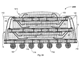
スタックドマルチパッケージアセンブリは、二つのカテゴリ、すなわち、いわゆるパッケージ・オン・パッケージ(PoP)アセンブリと、いわゆるパッケージ・イン・パッケージ(PiP)アセンブリとに一般的に分類される。 Stacked multi-package assemblies are generally classified into two categories: so-called package-on-package (PoP) assemblies and so-called package-in-package (PiP) assemblies.
2積層PoPマルチパッケージモジュールの例は、例えば2003年10月8日に出願された同時係属アメリカ合衆国出願No.10/681,572に示される。一例として、(「ボトム」パッケージといわれる)第一パッケージは、BGA回路基板のダイ接合側(「上方」側)に取り付けられ電気的に接続されたダイを有して、そして、ダイと電気的な接続点とを覆っているモールドキャップを提供するためにキャビティを形成し、しかし、露出した回路基板のダイ接合側の縁部を残している標準的なBGAと同様である。ダイ付着側(すなわち 「ランド」側といわれる「下方」側)に対するボトムパッケージ回路基板側は、例えばマザーボードのような、基礎をなす回路を有するモジュールの第二段階の相互接続のために半田ボールを備えている。(「トップ」パッケージといわれる)第二パッケージは、ボトムパッケージの上に積層され、それらは、ボトムパッケージのダイ接合側の露出された縁部で相互接続側に基づくために、トップパッケージのランド面上に備えられた半田ボールがトップパッケージ回路基板の面に配置されることを除いては、標準的なBGAとまた同様である。ボールを配置した周辺は、ボトムパッケージで相互接続側に配置された周辺と接続されその上リフローで接合する場合、それらは、ボトムBGAのモールドキャップへの干渉なしにZ相互接続をもたらす。上面パッケージダイ及び電気的接続部もまたカプセル化される。 An example of a two-layer PoP multi-package module is disclosed in, for example, copending United States application no. 10 / 681,572. As an example, a first package (referred to as a “bottom” package) has a die attached to and electrically connected to the die-joining side (“upper” side) of the BGA circuit board and is electrically connected to the die. This is similar to a standard BGA that forms a cavity to provide a mold cap overlying the connection points, but leaves the edge of the exposed circuit board die bonded side. The bottom package circuit board side relative to the die attach side (ie, the “down” side, referred to as the “land” side) provides solder balls for the second stage interconnection of modules with underlying circuitry, such as a motherboard. I have. The second package (referred to as the “top” package) is stacked on top of the bottom package, and because they are based on the interconnect side at the exposed edge of the die attach side of the bottom package, the land surface of the top package Similar to a standard BGA, except that the solder balls provided above are placed on the surface of the top package circuit board. When the periphery where the balls are placed is connected to the periphery located on the interconnect side in the bottom package and joined with reflow on top of them, they provide a Z interconnect without interference with the mold cap of the bottom BGA. The top package die and electrical connections are also encapsulated.
PoPモジュールで用いられるZ相互接続の型は、トップ及びボトムパッケージ回路基板がZ相互接続ボールとしてパッドに適合するように設計されることを要求する。パッケージの1つが、回路基板が異なったパッドの配列(異なる大きさや異なるデザイン)を有するものと交換される場合、他のパッケージの回路基板はその時それに応じて再設計される必要がある。これはマルチパッケージモジュールの製造にかかるコストの増大につながる。PoP設計において、トップ及びボトムパッケージの間隔は0.25mm或いはそれ以上あり、そして通常それは0.5mmから1.5mmの間の範囲であり、多くのダイに基づいており、ダイから回路基板への電気的接続がフリップチップであれ或いはワイヤボンドであれ基づいているボトムパッケージのカプセル高さと少なくとも同じ大きさでなければならない。例えば、ボトムパッケージのダイを接着された1つのワイヤにとって、300umのモールドキャップは75umの厚みのダイを通常適合できる。Z相互接続半田ボールは、一般的にそれらがリフローで接合された時に、それらがボトムBGAと接合するパッドとの接触を保証するにトップパッケージのランド面とボトムパッケージモジュールキャップの下面との間で接触なしに十分に大きい直径のものでなければならない。すなわち、半田ボールの直径は、リフローの間の半田ボールカプセルを考慮に入れ、加えてボールと回路基板との間のカプセル化しないものの許容範囲の総計によるカプセル高さよりも大きくなくてはならない。カプセル化されたボールの高さとボトムモールドキャップの高さとの間の標準的な設計の差(付加的な隙間)は約25umである。厚み約300umを有するモールドキャップにとっては、例えば、300umより大きいZ相互接続の半田ボールが採用されなければならない。より大きいボール直径は、より大きいボール間隔(一般的に、例えば、300umに対して約0.65mm間隔)を決定づける。それは次に、ボトムパッケージの回路基板の周辺における有効な空間に適合し得るボールの数を制限する。さらに、半田ボールの周辺機器の配置は、標準的なBGAのモールドキャップよりかなり大きくなることをボトムBGAに強いる。そして、半田ボールの周辺機器の配置は、全体的なパッケージサイズ(そのサイズはボール横列とボール間隔との数により増加させる。)を増大させる。標準的なBGAの本体サイズはモールドキャップより約2〜3mm大きい程度である。さらに、POPの構成機器のトップパッケージは、ずっと少ない相互接続を具備する小さいチップを含むかもしれないが、ボトムパッケージのそれと同じくらいのサイズで作られなければならない。ボール接合(例えば、ボールの付加的な横列)のためより大きい範囲を必要するため、パッケージの設置面積を増大させることは、特定の適用のための大きさの制限を超えることとなる。そしてどのような場合でも、より長いワイヤボンドとより大きい回路基板範囲とが必要となり、その両方がこれらの構成要素のコストを増大させる。パッケージ間の相互接続の数を増やすことは、回路基板の電気的接続における工程計画を容易にするための少なくとも2つ(しばしば2つ以上)の金属層をトップパッケージ回路基板が有することを要求することとなる。ある適用においてボトムパッケージの2つのダイを積層することは、上述の問題を悪化させ、ボトムモールドキャップが実に厚くなるということを引き起こすために、これはPoPの構成機器において実用的ではないかもしれない。 The type of Z interconnect used in the PoP module requires that the top and bottom package circuit boards be designed to fit the pads as Z interconnect balls. If one of the packages is swapped for one where the circuit board has a different pad arrangement (different size or different design), then the circuit board of the other package needs to be redesigned accordingly. This leads to an increase in cost for manufacturing the multi-package module. In PoP designs, the spacing between the top and bottom packages is 0.25 mm or more, and usually it is in the range between 0.5 mm and 1.5 mm and is based on many dies, from die to circuit board. It must be at least as large as the capsule height of the bottom package on which the electrical connection is based on flip chip or wire bond. For example, for a single wire with a bottom package die attached, a 300um mold cap can usually accommodate a 75um thick die. Z-interconnect solder balls are generally between the land surface of the top package and the bottom surface of the bottom package module cap to ensure contact with the pads that join the bottom BGA when they are joined by reflow. Must be of a sufficiently large diameter without contact. That is, the diameter of the solder ball must be larger than the total capsule height of what is not encapsulated between the ball and the circuit board, taking into account the solder ball capsule during reflow. The standard design difference (additional gap) between the encapsulated ball height and the bottom mold cap height is about 25 um. For a mold cap having a thickness of about 300 um, for example, Z interconnect solder balls larger than 300 um must be employed. Larger ball diameters dictate larger ball spacing (typically, for example, about 0.65 mm spacing for 300 um). It then limits the number of balls that can fit in the available space around the bottom package circuit board. In addition, the placement of solder ball peripherals forces the bottom BGA to be significantly larger than a standard BGA mold cap. And the placement of solder ball peripherals increases the overall package size (the size increases with the number of ball rows and ball spacing). The standard BGA body size is about 2-3 mm larger than the mold cap. In addition, the top package of POP components may include a small chip with much fewer interconnects, but must be made as large as that of the bottom package. Increasing the package footprint would exceed the size limit for a particular application, as a larger range is required for ball bonding (eg, additional rows of balls). And in any case, longer wire bonds and larger circuit board ranges are required, both of which increase the cost of these components. Increasing the number of interconnections between packages requires the top package circuit board to have at least two (and often more than two) metal layers to facilitate process planning in circuit board electrical connections. It will be. This may not be practical in PoP components because stacking the two dies of the bottom package in some applications exacerbates the above problem and causes the bottom mold cap to be really thick. .
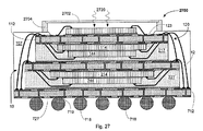
トップ及びボトムパッケージ回路基板の上方に面する側の間のワイヤボンドによるZ相互接続を有する2積層PiPモジュールの例としては、2003年8月2日に出願された同時係属のアメリカ合衆国出願No.10/632,549と2003年10月8日に出願された同時係属のアメリカ合衆国出願No.10/681,572とにおいて例えば示される。PiP構成機器において、トップパッケージは、ボトムパッケージ(すなわち、同じ方向に面している両方のパッケージ回路基板のダイ接合側を有して)に対して同じ方向にも配置されることとなり;或いは、トップパッケージは、ボトムパッケージ(すなわち、お互いに面している対照的なパッケージ回路基板のダイ接合側を有して)に対してひっくり返されることとなる。第二段階の相互接続の半田ボールは、例えばマザーボードのような基礎的な回路を有するモジュールの接続のためのボトムパッケージ回路基板のランド面の上に備えられる。トップパッケージがひっくり返される構成機器において、Z相互接続ワイヤボンドは、ボトムパッケージ回路基板のダイ接合側の上の周辺に配置されたワイヤボンド位置を具備するトップ回路基板のランド面にワイヤボンド位置に接続する。トップ及びボトムパッケージが同じように配置される場合には、Z相互接続ワイヤボンドは、周辺に配置されたワイヤボンド部を具備するトップ回路基板のボトムパッケージ回路基板のダイ接合側で周辺に配置されたワイヤボンド部を接続する。両方の構成機器において、トップパッケージは、ワイヤボンド加工を適用するためのボトムパッケージよりも小さい(Z相互接続を有する各々の余裕で少なくとも0.5mmより狭く及び/又はより短い)必要がある。 An example of a two-stack PiP module having a Z-connect by wire bond between the top facing side of the top and bottom package circuit boards is described in co-pending United States application no. 10 / 632,549 and copending United States application no. 10 / 681,572, for example. In a PiP component, the top package will also be placed in the same direction with respect to the bottom package (ie, having the die bond side of both package circuit boards facing the same direction); or The top package will be turned over with respect to the bottom package (i.e., with the die-bonded sides of the opposite package circuit board facing each other). The second stage interconnect solder balls are provided on the land surface of the bottom package circuit board for the connection of a module having a basic circuit such as a motherboard. In components where the top package is flipped, the Z interconnect wire bond connects to the wire bond location on the land surface of the top circuit board with the wire bond location located on the periphery on the die-bonded side of the bottom package circuit board To do. When the top and bottom packages are arranged in the same way, the Z interconnect wire bond is placed at the periphery on the die bonding side of the bottom package circuit board of the top circuit board with the wire bond portion located at the periphery. Connect the wire bond part. In both components, the top package needs to be smaller than the bottom package for applying wire bonding (at least less than 0.5 mm and / or shorter with each margin with Z interconnect).
PoPモジュールとPiPモジュールとは、トップパッケージとパッケージ間のワイヤボンド相互接続とを全体に覆うオーバーモールドにより仕上げられる。一旦、モジュールがオーバーモールドされたらもはや集積化は成し得ない。すなわち、設計者は、生産アセンブリ段階で(すなわち、面マウントアセンブリ段階で)アセンブリを再設計するための自由度を持たず、そして、相手先商標製品の製造会社は、コストを削減するためにさまざまな供給業者からさまざまなパッケージをうまく組み合わせることができない。 The PoP module and the PiP module are finished by overmolding that covers the entire top package and wire bond interconnections between the packages. Once the module is overmolded, integration can no longer be achieved. That is, the designer does not have the freedom to redesign the assembly at the production assembly stage (ie, at the face-mount assembly stage), and the original product manufacturer has various options to reduce costs. Cannot combine various packages from different suppliers.
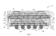
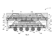
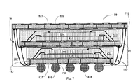
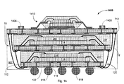
本発明は、モールディング側と回路基板側とを有するモールドされた第一(「トップ」)チップスケールパッケージとトップチップスケールパッケージの回路基板側に接合された第二(「ボトム」)パッケージとを備え、該第二パッケージは、第一と第二パッケージ回路基板との間をワイヤボンディングにより第一パッケージへ電気的に接続されており、スタックドCSP(チップスケールパッケージ)モジュールの一般的特徴である。本発明は、チップスケールパッケージの積層及び電気的相互接続(「Z相互接続」)を備え、実施例において、モールドされた基板とソーダイシングされたチップスケールパッケージの積層と電気的相互接続(「Z相互接続」)とを備える。 The present invention comprises a molded first (“top”) chip scale package having a molding side and a circuit board side and a second (“bottom”) package bonded to the circuit board side of the top chip scale package. The second package is electrically connected to the first package by wire bonding between the first and second package circuit boards, and is a general feature of a stacked CSP (chip scale package) module. The present invention comprises stacking and electrical interconnections of chip scale packages (“Z interconnects”), and in an embodiment, stacking and electrical interconnections of molded substrate and sodiced chip scale packages (“Z interconnects”). Interconnects)).
また、本発明は、第一パッケージ回路基板のダイ接合側と適合し電気的に相互接続される少なくとも1つの第一パッケージを含みモールドされ半田ボールを有さない第一(「トップ」)チップスケールパッケージを供給し、第一パッケージ回路基板のランド面に接着剤を塗布しており、第二パッケージ回路基板のダイ接合側と接合され電気的に相互接続されている少なくとも1つの第二パッケージを含むダイシングされてモールドされ半田ボールを有さない第二(「ボトム」)パッケージを供給し、第一パッケージ回路基板のランド面の上に第二パッケージを加え、その第二パッケージのモールディング面が第一パッケージ回路基板のランド面の接着剤に接触しており、接着剤を除去し、プラズマ除去を形成し、第二パッケージ回路基板のランド面と第一パッケージ回路基板のランド面の縁領域の部分との間のワイヤボンド相互接続を形成し、プラズマ除去を形成し、縁領域の中へ配置される第二回路基板のランド面の露出した領域をそのままにして、第一回路基板のランド面の縁領域、及びZ相互接続ワイヤボンドとワイヤループ、及び第二パッケージの頂点、及び第二パッケージのランド面の縁領域を取り囲むための操作を形成して、第二パッケージ回路基板の露出された領域の部分へ第二段階相互接続半田ボールを接合し、(第一回路基板がストリップ又はアレイを備えられた場合)ユニットアセンブリを完成するためにソーダイシングして成るスタックドチップスケールモジュール製造方法である。 The present invention also includes a first ("top") chip scale that includes at least one first package that is compatible and electrically interconnected with the die-bonding side of the first package circuit board and has no solder balls. Including at least one second package that is supplied and packaged with adhesive applied to a land surface of the first package circuit board and is electrically interconnected to the die-bonding side of the second package circuit board Supply a second ("bottom") package that is diced and molded and does not have solder balls, add the second package on the land surface of the first package circuit board, and the molding surface of the second package is the first In contact with the adhesive on the land surface of the package circuit board, the adhesive is removed, plasma removal is formed, and the second package circuit board label is removed. Forming a wire bond interconnect between the gate surface and the portion of the edge area of the land surface of the first package circuit board, forming a plasma removal and of the land surface of the second circuit board disposed in the edge area Leave the exposed area as it is to surround the edge area of the land surface of the first circuit board, and the Z interconnect wire bonds and wire loops, the apex of the second package, and the edge area of the land surface of the second package. Form an operation to join the second stage interconnect solder balls to portions of the exposed area of the second package circuit board (if the first circuit board is provided with a strip or array) to complete the unit assembly. Therefore, a stacked chip scale module manufacturing method is performed by sodicing.
他の一般的特徴として、本発明は、モジュール回路基板をひっくり返して搭載され電気的に相互接続された第一及び第二CSPスタックドパッケージを有するスタックドCSPアセンブリを提供する。第二CSPパッケージを有する第一CSPパッケージさらにモジュール回路基板を有するCSPパッケージのZ相互接続は、モジュール回路基板のパッケージ接合側を有するそれぞれのCSPパッケージ回路基板のランド面を接続しているワイヤボンドにより構成される。第二段階相互接続と付加的な構成要素を有する相互接続がなされることがあるため、(アセンブリの一側面で)モジュール回路基板と(アセンブリのそれに対向する側で)第一CSPパッケージ回路基板の部分とが露出されるようにアセンブリはカプセル化される。 As another general feature, the present invention provides a stacked CSP assembly having first and second CSP stacked packages that are mounted and electrically interconnected with the module circuit board upside down. The Z interconnection of the first CSP package having the second CSP package and the CSP package having the module circuit board is made by wire bonding connecting the land surfaces of the respective CSP package circuit boards having the package joint side of the module circuit board. Composed. Because a second stage interconnect and an interconnect with additional components may be made, the module circuit board (on one side of the assembly) and the first CSP package circuit board (on the opposite side of the assembly) The assembly is encapsulated so that the parts are exposed.
実施例において、アセンブリの第一CSPパッケージ側は第二段階相互接続側であり、即ち、(例えばマザーボードのような)基礎となる回路へのアセンブリの第二段階相互接続は、第一CSPのランド面の露出された領域のランドで半田ボール(又は電気的接続手段)による。従って、モジュール回路基板の露出されたランド面はアセンブリに積層される付加的な構成要素を有する相互接続に利用される。さらに、その時、本発明は、アセンブリの一側面で露出されたモジュール回路基板とアセンブリの他方の側で露出された第一CSPパッケージ回路基板の部分とを有して、さらにCSPパッケージ回路基板の露出された部分で形成される第二段階相互接続とLGAパッケージ回路基板で1つ以上の付加的な構成要素を有する相互接続とを有するスタックドパッケージアセンブリを特徴とする。一部実施例では、付加的な構成要素は、積層されたダイBGAであるボールグリッドアレイ(BGA)パッケージ、或いは積層されたダイLGAである付加的なLGA、或いは積層されたダイクワッドフラットパッケージ(SD QFP)であるクワッドフラットパッケージ(QFP)、或いは積層されたダイクワッドフラットパッケージ(SD QFP)であるクワッドフラット無鉛(QFN)パッケージ又はリードフレームチップスケールパッケージ(LFCSP)、或いは一帯モールドされるワイヤボンドされたダイ(又はワイヤボンドされたダイのスタック)、或いは光学センサパッケージ、或いは微小電気機械センサ(MEMS)パッケージを1つ以上含み、従って、付加的な構成要素は1つ以上の受動機器を備えることとなる。一部実施例では、熱拡散器がモジュール回路基板の露出されたランド面に搭載される。 In an embodiment, the first CSP package side of the assembly is the second stage interconnect side, i.e., the second stage interconnect of the assembly to the underlying circuitry (e.g., a motherboard) is the first CSP land. By solder balls (or electrical connection means) on the land in the exposed area of the surface. Thus, the exposed land surface of the module circuit board is utilized for interconnections with additional components laminated to the assembly. Further, then, the present invention comprises a module circuit board exposed on one side of the assembly and a portion of the first CSP package circuit board exposed on the other side of the assembly, and further exposing the CSP package circuit board. And a stacked package assembly having a second stage interconnect formed by the formed portions and an interconnect having one or more additional components on the LGA package circuit board. In some embodiments, the additional component may be a ball grid array (BGA) package that is a stacked die BGA, or an additional LGA that is a stacked die LGA, or a stacked diquad flat package ( SD QFP) Quad Flat Package (QFP), Stacked Die Quad Flat Package (SD QFP) Quad Flat Lead Free (QFN) Package or Leadframe Chip Scale Package (LFCSP), or Single Bond Molded Wire Bond One or more of a die (or a stack of wire bonded dies), or an optical sensor package, or a microelectromechanical sensor (MEMS) package, so that the additional components comprise one or more passive devices It will be. In some embodiments, the heat spreader is mounted on the exposed land surface of the module circuit board.
発明の他の一般的特徴として、アセンブリのモジュール回路基板は第二段階相互接続側であり、即ち、(例えばマザーボードのような)基礎となる回路へのアセンブリの第二段階相互接続は、第一CSPのランド面の露出された領域のランドで半田ボール(又は電気的接続手段)によるものである。従って、CSP回路基板の露出されたランド面はアセンブリに積層される付加的構成要素を有する相互接続に利用される。さらに、その時、本発明は、アセンブリの一側面で露出されたモジュール回路基板とアセンブリの他方の側で露出された第一CSPパッケージ回路基板の部分との両方を有して、さらにモジュール回路基板の露出された部分で形成されたダイに段階相互接続と露出されたCSPパッケージ回路基板で1つ以上の付加的な構成要素を有する相互接続とを有する積層パッケージアセンブリを特徴とする。一部実施例では、付加的構成要素は、積層されたダイBGAであるボールグリッドアレイ(BGA)パッケージ、或いは積層されたダイLGAである付加的なLGA、或いは積層されたダイクワッドフラットパッケージ(SD QFP)であるクワッドフラットパッケージ(QFP)、或いは積層されたダイクワッドフラットパッケージ(SD QFP)であるクワッドフラット無鉛(QFN)パッケージ又はリードフレームチップスケールパッケージ(LFCSP)、或いは一帯モールドされるワイヤボンドされたダイ(又はワイヤボンドされたダイのスタック)、或いは光学センサパッケージ、或いは微小電気機械センサ(MEMS)パッケージを1つ以上含み、従って、付加的な構成要素は1つ以上の受動機器を備えることとなる。一部実施例では、熱拡散器が第一CSPパッケージの露出されたランド面に搭載される。 As another general feature of the invention, the modular circuit board of the assembly is on the second stage interconnect side, i.e. the second stage interconnect of the assembly to the underlying circuit (such as a motherboard) is This is due to the solder balls (or electrical connection means) in the exposed areas of the CSP land surface. Thus, the exposed land surface of the CSP circuit board is utilized for interconnections with additional components laminated to the assembly. Further, then, the present invention comprises both a module circuit board exposed on one side of the assembly and a portion of the first CSP package circuit board exposed on the other side of the assembly, and further comprising a module circuit board Featuring a stacked package assembly having a staged interconnect on a die formed of exposed portions and an interconnect having one or more additional components on an exposed CSP package circuit board. In some embodiments, the additional component is a ball grid array (BGA) package that is a stacked die BGA, or an additional LGA that is a stacked die LGA, or a stacked diquad flat package (SD). QFP) Quad Flat Package (QFP), Stacked Die Quad Flat Package (SD QFP) Quad Flat Lead Free (QFN) Package or Leadframe Chip Scale Package (LFCSP) One or more dies (or a stack of wirebonded dies), or optical sensor packages, or microelectromechanical sensor (MEMS) packages, so that the additional components comprise one or more passive devices It becomes. In some embodiments, a heat spreader is mounted on the exposed land surface of the first CSP package.
一部実施例では少なくとも1つの第一及び第二CSPパッケージがスタックドダイパッケージである。 In some embodiments, the at least one first and second CSP package is a stacked die package.
一部実施例では、第一(「トップ」)パッケージがモールドされソーダイシングされた基板であり、ある実施例では第一パッケージがモールドされたキャビティである。ある実施例では第二(「ボトム」)パッケージがモールドされソーダイシングされた基板であり、ある実施例では第二パッケージがモールドされたキャビティである。 In some embodiments, a first (“top”) package is a molded and sodiced substrate, and in certain embodiments, the first package is a molded cavity. In one embodiment, the second (“bottom”) package is a molded and sodiced substrate, and in one embodiment, the second package is a molded cavity.
本発明はすぐれた製造可能性と高いデザイン自由度とを備え、薄型で小さい設置面積を有する積層パッケージモジュールを低コストで生産できる。 The present invention is capable of producing a low-cost laminated package module having excellent manufacturability and high design freedom, and having a thin and small installation area.
CSPと他のパッケージとが最も低コストと最も広い有用性との選択的に提供することは工業においての標準的なことである。 It is standard in the industry that CSP and other packages selectively provide the lowest cost and the widest utility.
標準的な単一のワイヤボンドされたダイCSP厚さは0.8mmである。本発明によるCSPの回路基板のランド面の第二パッケージの積層は、10〜50ミクロンの範囲の完成厚さを有する接着剤を用いることを可能とする。本発明によるモジュールの設置面積はスタックの最大チップサイズにより決定される。ワイヤボンドZ相互接続は、回路基板に金属端面を短絡することなしにワイヤを適合するために約0.5mmから1.0mmの間で第二回路基板より小さいボトムCSPを通常要求する。選択されたボトムCSPパッケージがトップ回路基板よりも著しく小さいので、ワイヤボンディングは、少なくとも8mm又はそれ以上まで異なる大きさを適合することができる。従って、所定の選択されたCSPにとって、CSPより著しく大きい設置面積を有するトップ回路基板の選択が可能となる。このことは、アセンブリに積層された付加的な構成要素を選択するため、設計者にとって非常に自由度が高いものを提供する。 A standard single wire bonded die CSP thickness is 0.8 mm. Lamination of the second package on the land surface of the CSP circuit board according to the present invention allows the use of an adhesive having a finished thickness in the range of 10-50 microns. The footprint of the module according to the present invention is determined by the maximum chip size of the stack. Wirebond Z interconnects usually require a bottom CSP between about 0.5 mm and 1.0 mm smaller than the second circuit board to fit the wire without shorting the metal end face to the circuit board. Since the selected bottom CSP package is significantly smaller than the top circuit board, wire bonding can accommodate different sizes up to at least 8 mm or more. Thus, for a given selected CSP, it is possible to select a top circuit board having a significantly larger footprint than the CSP. This provides a great degree of freedom for the designer to select additional components stacked in the assembly.
本発明によるパッケージアセンブリは、コンピュータを構築することや通信機器及び消費者及び工業エレクトロニクスデバイスに用いられる。 The package assembly according to the present invention is used in building computers, communication equipment and consumer and industrial electronics devices.
また、本発明に係るスタックドパッケージモジュールにおいて、ランド面で外部と電気的に接続されるためのモジュール回路基板と、モジュール回路基板のパッケージ接合側に搭載された第一チップスケールパッケージであって、モジュール回路基板とワイヤボンドで電気的に接続される第一パッケージ回路基板と、第一パッケージ回路基板のダイ接合側に接合された第一パッケージダイと、モジュール回路基板に搭載されるための面を有する第一パッケージモールディングとを備える第一チップスケールパッケージと、第一パッケージ回路基板のランド面に搭載された第二チップスケールパッケージであって、第一パッケージ回路基板とワイヤボンドで電気的に接続される第二パッケージ回路基板を備える第二チップスケールパッケージと、ワイヤボンドを囲んで保護し、しかも、モジュール回路基板のランド面と第二パッケージ回路基板のランド面の一部との両方が露出されるように設けられているモジュールモールディングとを備えていることを特徴とする。 Further, in the stacked package module according to the present invention, a module circuit board for being electrically connected to the outside on the land surface, and a first chip scale package mounted on the package joint side of the module circuit board, A first package circuit board electrically connected to the module circuit board by wire bonding, a first package die bonded to the die bonding side of the first package circuit board, and a surface to be mounted on the module circuit board a first chip-scale package Ru and a first package molding having, a second chip-scale package mounted on the land surface of the first package circuit board, electrically connected by the first package circuit board and wire bonds A second chip scale package comprising a second package circuit board Protect surrounding the wire bonding, moreover, that it is a module moldings both a part of the land surface of the module circuit board and the land surface of the second package circuit board is provided so as to expose Features.
特に、請求項1記載のモジュールにおいて、モジュール回路基板のランド面の部分でマザーボードのような基礎となる回路に接続されることが好ましい。 In particular, in the module according to claim 1, wherein, Rukoto are connected by portions of the land surface of the module circuit board to the underlying circuit, such as a motherboard is preferred.
また更に、請求項1記載のモジュールにおいて、第二パッケージ回路基板のランド面の露出された部分の位置でマザーボードのような基礎となる回路に接続されることが好ましい。 Still further, in the module according to claim 1, it is preferable that the second package circuit board is connected to a base circuit such as a mother board at a position of an exposed portion of a land surface of the second package circuit board.
更に、請求項1記載のモジュールにおいて、モジュール回路基板のランド面に搭載し電気的に接続された付加的な機器を備えることが好ましい。 Further, in the module according to claim 1, wherein the module circuitry Rukoto with additional device mounted electrically connected to the land surface of the substrate it is preferred.
また、請求項4記載のモジュールにおいて、付加的な機器がダイを含むことが好ましい。 Further, in the module according to claim 4, it is preferable that the additional equipment includes a die.
また更に、請求項4記載のモジュールにおいて、付加的な機器が半導体パッケージを含むことが好ましい。 Still further, in the module according to claim 4, it is preferable that the additional device includes a semiconductor package.
また、請求項4記載のモジュールにおいて、付加的な機器が受動機器を含むことが好ましい。 In the module according to claim 4, it is preferable that the additional device includes a passive device.
また、請求項1記載のモジュールにおいて、第二パッケージ回路基板のランド面の露出された部分に搭載され電気的に接続された付加的な機器を備えることが好ましい。 The module according to claim 1 is preferably provided with an additional device mounted on and electrically connected to the exposed portion of the land surface of the second package circuit board.
更に、請求項8記載のモジュールにおいて、付加的な機器がダイを含むことが好ましい。 Furthermore, in the module of claim 8, it is preferred that the additional equipment comprises a die.
また、請求項8記載のモジュールにおいて、付加的な機器が受動機器を含むことが好ましい。 In the module according to claim 8, it is preferable that the additional device includes a passive device.
また更に、請求項8記載のモジュールにおいて、付加的な機器が半導体パッケージを含むことが好ましい。 Still further, in the module according to claim 8 , the additional device preferably includes a semiconductor package.
本発明は、本発明の選択的な実施形態を示す図面を参照することによって、ここにさらに詳しく説明される。図は、本発明の特徴と、それらと他の特徴及び構成との関係とを示す概略図であり、一定の比率ではない。説明の一層の明確化のために、本発明の実施形態を示す図において、他の図面において示される要素と一致する要素すべては、すべての図においてすぐに同一視可能であるが、特に名称を付けているわけではない。 The invention will now be described in further detail by reference to the drawings, which show alternative embodiments of the invention. The figure is a schematic diagram showing the features of the present invention and the relationship between them and other features and configurations, not to a certain ratio. For further clarity of explanation, in the figures showing the embodiments of the present invention, all elements that coincide with elements shown in the other drawings can be immediately identified in all the figures, but in particular the names Not attached.
以下のある時点で、「水平な」、「垂直な」、「上に」、「上側に」、「下側に」、「上の」、「下の」、「トップ」、「ボトム」、「上方の」、「下方の」、及びその他のような相対配向の条件が、図において示される特徴の相対配向と関連して用いられることとなる。認識されることとして、本発明に従うさまざまなアセンブリは、ユーザにおいて或いは工程の間でどんな配置にもあてはめられる。 At some point below, “horizontal”, “vertical”, “up”, “up”, “down”, “up”, “down”, “top”, “bottom”, Relative orientation conditions such as “upper”, “lower” and others will be used in conjunction with the relative orientation of the features shown in the figure. It will be appreciated that the various assemblies according to the present invention can be applied to any arrangement at the user or between processes.
ここに参照されたすべての特許及び特許出願は、ここに参照されることによってここに組み込まれる。 All patents and patent applications referred to herein are hereby incorporated by reference herein.
図1を参照すると、1で半田ボールのない一般的なチップスケールパッケージと、モールドされた基板と、ソーダインジングとの概略断面図が示される。図1で示されるCSP1は、少なくとも1つの金属層を有する回路基板112の上に接合されたダイ114を含む。さまざまな回路基板の型のどれもが、例えば:2〜6の金属層を有する積層板、或いは4〜8の金属層を有する構築された回路基板、或いは1〜2の金属層を有する弾力性のあるポリイミドテープ、或いはセラミック多層構造の回路基板を含みながら使用されることとなる。図1に一例として示される回路基板112は、適切な回路を提供するために各々がパターン化されたバイス122を手段として接続された2つの金属層121、123を備える。ダイは、接着剤を用いる回路基板の面に従来接合され、一般的にはダイ接合エポキシと呼ばれ、図1の113で示され、そして、ダイ接合側が使用の際にある特性の配置を有する必要がないけれども、図1の構成機器において、ダイが接合される(「ダイ接合」側)の上の回路基板の側が「上方の」側と呼ばれることとなる。
Referring to FIG. 1, there is shown a schematic cross-sectional view of a typical chip scale package 1 with no solder balls, a molded substrate, and soda inging. The CSP 1 shown in FIG. 1 includes a die 114 bonded onto a
図1のCSPパッケージにおいて、ダイは、電気的接続を開設するための回路基板の上方の金属層のワイヤボンド側の上の接合されたワイヤである。ダイ114とワイヤボンド116とは、モールドされた基板とソーダインシングとによる本例において、取り扱い作業を容易にするために周辺及び機械的なストレスからの保護を提供する成形材料117を具備してカプセル化される。接着パッド119はパッケージを試験するため或いは他の特性に対する又は例えばマザーボード(図示しない)の基礎回路に対するパッケージの第二段階相互接続のために回路基板112の下方の金属層123に備えられる。ソルダーレジスト115、127は、電気的接続のための接着側、例えば、ワイヤボンド側で基礎となる金属及びワイヤボンド116と他の主要なものとを接着するための接着パッド、又は第二段階相互接続のための半田ボールを露出するための金属層121、123一面にパターン化される。
In the CSP package of FIG. 1, the die is a bonded wire on the wire bond side of the metal layer above the circuit board for establishing electrical connections. The
第二段階相互接続ボールパッド119は、マザーボードのような、基礎回路に対してCSPの付属品を提供する。
The second stage
図2は、一般的に2で、本発明による積層されたCSPモジュールを示している概略断面図である。ここで、「ボトム」CSP120は、CSP回路基板112のダイ接合側の上へ加えられたダイ114と144とを備えて、また、第一ダイを回路基板へ接合し、第二ダイを第一ダイへ接合するための接着剤を使用する積層されたダイCSPである。ダイは、ワイヤボンド116、146により回路基板へ電気的に相互接続される。ダイ114と144及びワイヤボンド116と146とは、基板成形とソーダイシングとにより、周辺及び機械的なストレスからの保護を提供して、第二(「トップ」)パッケージが積層され得る229上面のボトムパッケージ成形材料117を有してカプセル化される。
FIG. 2 is a schematic cross-sectional view showing a stacked CSP module, generally 2, according to the present invention. Here, the “bottom”
さらに図2を参照すると、第二(「トップ」)パッケージは、第一側と第二側、及び少なくとも1つの金属層、及びダイ244と積層され回路基板12へワイヤボンドされた214とを含んでモールドされた基板とソーダイシングされたCSP10とを同様に構成される。図2に一例として示される回路基板12は、適合した回路を各々パターン化され、バイス22手段で接続された2つの金属層21と23とを有する。第一パッケージと面する第二回路基板の側は、「ランド」側と呼ばれるアセンブリである。
Still referring to FIG. 2, the second (“top”) package includes a first side and a second side, and at least one metal layer, and 214 laminated with
図2における実施例の第二パッケージ回路基板12において、ソルダーレジスト12及び27は、電気的接続のための接着面、例えば、ワイヤボンド118を接着するためのワイヤボンド面で基礎をなす金属を露出するため金属層21及び23一面にパターン化される。
In the second
トップパッケージ10とボトムパッケージ120との間のZ相互接続は、ボトムパッケージ回路基板の下位の金属層123の回線を備えるトップ回路基板の金属層(金属層21)と下方で向かい合っている配線を接続しているワイヤボンド218手段により取り付けられる。一方で、トップ回路基板12の金属層21上にパッドの下方に向かい合っている面へ各々のワイヤボンド118が電気的に接続されると、もう一方では、各々のワイヤボンドが、ボトムパッケージ回路基板112の下位の金属層123上のパッドの下側の面に接続される。例えば、参照することによってここに組込まれるアメリカ合衆国5,226,582に記載されるような、当技術分野で周知のように、ワイヤボンドはいかなるワイヤ接着技術によっても形成されることとなる。トップ回路基板の下側の金属層のパッドの面上にビード又はバンプを形成して、そしてその時、ボトム回路基板の下側の金属層におけるパッドに向けてワイヤを張り、それを溶解することにより作られた時に、パッケージからパッケージへのZ相互接続ワイヤボンドは一例として図2に示される。上記内容からわかるように、逆方向に、すなわち、ボトム回路基板の下側の金属層パッドの下側の面上にビードやバンプを形成して、そしてその時、トップ回路基板の金属層のパッドに向けてワイヤを敷き、それを溶解することにより、ワイヤボンドは取り付けられることができる。上記内容からわかるように、パッケージからパッケージへのZ相互接続のためのワイヤボンディング方法の選択は、積層された回路基板とそれらの接着面との隙間の幾何学的配置に従って決定されることとなる。また、上記内容からわかるように、従来のワイヤボンディング装置においてワイヤボンドキャピラリーは、配置されたボンドパッドの上側へ下向きに取り付けられ、そして、実際には、アセンブリは、少なくともワイヤボンド手段のための発明によりひっくり返されることとなる。
The Z interconnection between the
さらに、トップパッケージ回路基板は取り付けられる第一パッケージのモールドキャップの面よりも大きく、ボンドパッドがワイヤボンド118から露出されたトップパッケージ回路基板の第一側の周辺範囲に残したままである。トップ回路基板は(実際に後では)パンチ又はソーダイシングされる。 Further, the top package circuit board is larger than the surface of the mold cap of the first package to be attached, leaving bond pads in the peripheral area on the first side of the top package circuit board exposed from the wire bonds 118. The top circuit board is punched or sodiced (actually later).
ボトムパッケージ基板のダイ接合側がモールドにより覆われるために、ボトムパッケージは、(図2の一例の)モールド及び(図2に示されるようにモールドのための垂直壁を備えるために)ソーダインシングされた基板である。ボトムパッケージ回路基板のダイ接合側の上方の金属層のボンドパッドは、ワイヤボンドによりダイと接続され、回路基板のダイ接合側へバイスを通じてボトムパッケージ回路基板のランド面の下方の金属層へ上方の金属層は接続され、ボトムパッケージ回路基板のランド面の下方の金属層は、Z相互接続ワイヤ118を有する接続のための周辺に配置されたボンドパッドを備えるためにパターン化される。
Because the die-bonding side of the bottom package substrate is covered by the mold, the bottom package is soda-insulated (to provide an example of FIG. 2) and a mold (as shown in FIG. 2 with vertical walls for the mold). Substrate. The bond pad of the metal layer on the upper side of the die bonding side of the bottom package circuit board is connected to the die by wire bonding, and is connected to the die bonding side of the circuit board through the vice to the metal layer below the land surface of the bottom package circuit board. The metal layers are connected and the metal layer below the land surface of the bottom package circuit board is patterned to provide bond pads located at the periphery for connection with
アセンブリの前に不適合なパッケージの排除を可能にするため、そして高度な最終モジュールテスト収率を保証するために、本発明による構造はCSPの予備試験を可能にする。 In order to allow the elimination of non-conforming packages prior to assembly and to ensure a high final module test yield, the structure according to the present invention allows CSP pre-testing.
図2の積層されたパッケージの実施例において、それぞれのパッケージ回路基板上のZ相互接続パッドはパッケージ回路基板の縁近くの金属層の上に配置される。トップパッケージ回路基板上のZ相互接続パッドがパッケージが積層された時にボトムパッケージ上の対応するZ相互接続パッドの上におおよそ被さるために、Z相互接続パッドの配置と順序は一般的に決められる。好都合なことに、回路基板の金属層の縁部に対して電気的に絶縁することなしにワイヤボンドのための隙間を設けるために、ボトムパッケージ120の設置面積より大きい回路基板の設置面積をトップ回路基板10は備える。
In the stacked package embodiment of FIG. 2, the Z interconnect pads on each package circuit board are disposed on a metal layer near the edge of the package circuit board. The placement and order of the Z interconnect pads is generally determined so that the Z interconnect pads on the top package circuit board roughly cover the corresponding Z interconnect pads on the bottom package when the package is stacked. Conveniently, the circuit board footprint is larger than the footprint of the
一旦、Z相互接続ワイヤボンドが積層された第一パッケージと第二回路基板との接続を形成したら、Z相互接続ワイヤボンドを囲んで保護するために、そして完成したアセンブリに対する機械的安全性を備えるために、アセンブリカプセル化207は形成される。アセンブリカプセル化207は、トップパッケージ回路基板の下を向いて直面しているランド面の縁の領域で覆い、Z相互接続ワイヤボンドとワイヤループと垂直壁とボトムパッケージの頂点とを取り囲み、そしてワイヤボンドが接続されているワイヤループとワイヤボンドパッドとを含むボトムパッケージ回路基板のランド面の縁の領域で覆う。このことは、第二段階相互接続のために露出されたボトムパッケージ回路基板のランド面の領域を残したままにする。図2を参照すると、半田ボール318は、例えば、コンピュータのような最終製品のマザーボード(図示しない)のような、基礎となる回路に対する相互接続を備えるために回路基板の下方の金属層の露出された領域の接着パッド119の上へリフローされる。
Once the connection between the first package laminated with the Z interconnect wire bond and the second circuit board is formed, it surrounds and protects the Z interconnect wire bond and provides mechanical safety to the finished assembly. For this, the
図2の一例として示されるように、モジュールはそれ自体でソーダイシングされる。或いは、モジュールはソーダイシングされるというよりむしろ個々にモールドされることとなる。あきらかなように、CSPパッケージは、ワイヤボンディングよりむしろ、第一パッケージ回路基板に対するダイのフリップチップの相互接続を備えることとなる。 As shown in the example of FIG. 2, the module is sodiced by itself. Alternatively, the modules will be molded individually rather than being sodiced. Clearly, the CSP package will provide die flip chip interconnection to the first package circuit board rather than wire bonding.
図5Aと5Bとは、図2の112で示されるような適合する第一パッケージ回路基板のそれぞれランド面とダイ接合側とを示す平面図における概略図である。図5Aを参照すると、ランド面の面のほとんどが、金属層の上の部分がソルダーレジストの開口により露出されることを除いて、パターン化された金属層の下でソルダーレジストにより覆われている。回路基板の端面52付近の余裕のある範囲に配置され、回路基板面の中間領域に配列されたボールパッド(例えば53)とボンドフィンガー(例えば56)とを含む回路基板のランド面でパターン化された金属層の部分をソルダーレジストの開口は露出する。ソルダーレジストにより覆い隠されるものは、ボールパッド53とボンドフィンガー56とを接続し、及び/又は、回路基板のダイ接合側でパターン化された金属層の配線を有して回路基板のランド面でパターン化された金属層の配線を電気的に接続するバイス(例えば522)を有するボールパッド53を接続する金属層の配線(例えば523)である。
5A and 5B are schematic views in plan view showing respective land surfaces and die-bonding sides of a suitable first package circuit board as shown at 112 in FIG. Referring to FIG. 5A, most of the land surface is covered by the solder resist under the patterned metal layer, except that the upper part of the metal layer is exposed by the opening of the solder resist. . It is arranged in a marginal area near the
さらに、アセンブリカプセル化は、ボンドパッド56とパッド56で形成されたワイヤループとを覆う。すなわち、カプセル化は、第一パッケージ回路基板のランド面の領域が最低限のカプセル化により拘束されているので、すなわち、破線58の中で、アセンブリモールディングの明らかにされた以下の構成のままであるので、破線58で図5Aに示された縁の領域に対して回路基板のランド面で制限される。従って、ボールパッド53は、例えば、(例えば図3に示されるような)基礎となる回路に対するアセンブリのZ水準の相互接続として半田ボールの接合として利用される。さらに、ボールパッド53は、アセンブリする前のパッケージをテストするための、或いは必要であれば、第二段階相互接続半田ボールを乗せる前のパッケージアセンブリをテストするためのテストプローブとして利用される。カプセル化された縁の領域は、ボンドフィンガーとボンドフィンガーに対する配線の長さとソーの通る幅との長さの合計により決められる幅(図5AにおけるMW)を有する。さらに、射出成形は、(図5Aの破線58で)縁側の内端で回路基板の面を明確にすることとなる。回路基板が細長いもの又は配列として設けられる場合、端部で回路基板の材料は、第一パッケージのソーダイシングの間のソー幅のために失われる。実際、ボンドフィンガー長は約250umであり、フィンガー配線長は約50umであり、そしてモールド樹脂抽出のための遊びは約500um必要となる。ソーは実際約50umを必要とする。
Further, the assembly encapsulation covers the
実際には、ボールパッド53の数と配列とは、カプセル化された場合、ボールがお互い接触或いは近接してはいけないので、ボールの呼び径に依存する。さらにまた、実際には、ボールパッド53の大きさと近接とは、配線と特にソルダーレジスト開口とを組み込むときの分解能の限界によって制限される。1つの実施例において、ボールパッドは、直径約280umの円形であり、中心間距離500umで四角形又は矩形の配列で並べられている。(ソルダーレジスト開口の最も近い端との距離は実際には中心間距離の0.2倍以下もない。)
Actually, the number and arrangement of the
ダイが接合された状態の第一パッケージ回路基板のダイ接合側は図5Bに示される。第一ダイ114は、回路基板のダイ接合側の上のアクティブな側の上方に加えられる。本例として、ダイは、四角形を規定する4つの頂点を備える。ワイヤボンドパッド51は、ダイの4つの頂点の近くに列をなして配置される。回路基板のランド面では、ダイ接合側の面のほとんどがソルダーレジストにより覆われるので、金属層の部分を以外では、ボンドフィンガー(例えば54)の特定の列(本実施例では、ダイの各々の頂点に沿った列)を含むソルダーレジストの開口により露出される。ソルダーレジストにより覆い被されたものは、ボンドフィンガー54をランド面でパターン化された金属層の配線を有する回路基板のダイ接合側でパターン化された金属層の配線を電気的に接続するバイス(例えば522)に対して接続する金属層の配線(例えば521)である。従って、第一パッケージダイは、第一パッケージ回路基板のダイ接合側の金属層の配線に対してワイヤ手段により、そしてランド面の金属層の配線とZ相互接続ワイヤボンドフィンガーとに対してバイス手段により接続される。Z相互接続ワイヤは、第二パッケージ回路基板のダイ接合側のボンドフィンガーに対して第一パッケージ回路基板のランド面のボンドフィンガーを接続する。第二ダイ114の設置面積は破線533により図5Bに示される。
The die bonding side of the first package circuit board with the die bonded is shown in FIG. 5B. A
トップパッケージ10の回路基板は図5Aと5Bとに同様に示される。
The circuit board of the
図3によると、ボトムスタックドダイと回路基板とはカプセル化される必要はない。ボトムパッケージダイが回路基板へワイヤボンドされた場合、ボトムダイのワイヤボンドを有するトップ回路基板の干渉を防ぐためにスペーサが設けられなければならない。 According to FIG. 3, the bottom stacked die and the circuit board need not be encapsulated. When the bottom package die is wire bonded to the circuit board, spacers must be provided to prevent interference of the top circuit board with the bottom die wire bond.
図4によると、トップパッケージの底面の1つ、或いは(図に示す)ボトム及びトップパッケージ両方は、モールド及びソーダイシングされた基板よりむしろモールドされたキャビティに違いない。 According to FIG. 4, one of the bottom surfaces of the top package or both the bottom and top packages (shown in the figure) must be a molded cavity rather than a molded and sodiced substrate.
図に示唆されるように、第二パッケージ回路基板は、パッケージ回路基板間のZ相互接続に適合するために第一パッケージ回路基板よりも広い設置面積が必要となる。実施例では、Z相互接続は、パッケージの4つ全ての頂点に沿って配列され、従って、第二パッケージは第一パッケージよりも広く且つ長くなる。本発明によるいくつかのアセンブリでわかるように、Z相互接続は、例えば1つの頂点のみ、又は対向する2つの頂点のような、4つ全ての頂点未満のボンドフィンガー間で使用されることとなる。(第二回路基板のより大きいダイがより大きい設置面積を必要としなければ、)そのような実施例では、第二パッケージは、単一の方向でのみ第一パッケージよりも大きい(長い又は広い)必要がある。 As suggested in the figure, the second package circuit board requires a larger footprint than the first package circuit board to accommodate the Z interconnection between the package circuit boards. In an embodiment, the Z interconnects are arranged along all four vertices of the package, so that the second package is wider and longer than the first package. As can be seen in some assemblies according to the present invention, Z interconnects will be used between bond fingers below all four vertices, eg only one vertex or two opposing vertices. . In such an embodiment (if a larger die on the second circuit board does not require a larger footprint), the second package is larger (longer or wider) than the first package only in a single direction. There is a need.
第一及び第二パッケージ回路基板はいくつかの多様な機能性を備えることとなる。例えば、CSPは、DSP又はASIC又はGPUになり得て、そしてLGAパッケージは、Flash又はDRAM又はSRAMのようなメモリになり得る。 The first and second package circuit boards will have several diverse functionalities. For example, the CSP can be a DSP or ASIC or GPU, and the LGA package can be a flash or memory such as DRAM or SRAM.
本発明の特徴によればフリップチップボトムパッケージのプロセッサチップは、例えばASIC又はGPU又はCPU又は時にASICになり得て、そしてトップパッケージは、例えばプロセッサチップ或いは例えばメモリパッケージ又はASICパッケージになり得る。トップパッケージがメモリパッケージである場合、それは、積層されたダイメモリパッケージとなり得る。シールドされたフリップチップダイアップボトムパッケージは、携帯通信アプリケーションの中のような特に無線周波処理のための高速アプリケーションに特に適合することができる。 According to a feature of the present invention, the processor chip of the flip chip bottom package can be, for example, an ASIC or GPU or CPU or sometimes an ASIC, and the top package can be, for example, a processor chip or, for example, a memory package or an ASIC package. If the top package is a memory package, it can be a stacked die memory package. The shielded flip chip die up bottom package can be particularly adapted for high speed applications, especially for radio frequency processing, such as in mobile communication applications.
第一パッケージはいくつかの多様な機能性を備えることとなる。例えば、CSPパッケージは、DSP又はASIC又はGPUになり得て、或いはCSPパッケージは、Flash又はDRAM又はSRAMのようなメモリになり得る。 The first package will have several diverse functionalities. For example, the CSP package can be a DSP or ASIC or GPU, or the CSP package can be a memory such as Flash or DRAM or SRAM.
本発明の特徴によればフリップチップボトムパッケージのプロセッサチップは、例えばASIC又はGPU又はCPU又は時にASICになり得る。トップパッケージがメモリパッケージである場合、それは、積層されたダイメモリパッケージとなり得る。シールドされたフリップチップダイアップボトムパッケージは、携帯通信アプリケーションの中のような特に無線周波処理のための高速アプリケーションに特に適合することができる。 According to a feature of the invention, the processor chip of the flip chip bottom package can be, for example, an ASIC or GPU or CPU or sometimes an ASIC. If the top package is a memory package, it can be a stacked die memory package. The shielded flip chip die up bottom package can be particularly adapted for high speed applications, especially for radio frequency processing, such as in mobile communication applications.
図6は、図2のようなアセンブリを製作するための工程の手順を示しているフローチャートである。ステップ602において、“第一”CSPは、通常“第一”CSPのダイシングされないストリップとして備えられている。ステップ604において、接着剤は、“第一”CSPの露出したランド面の上へ塗布される(例えば粘着フィルムとして貼り付けられ又は設けられる)。ステップ606において、“第二”CSPは設けられ、そしてステップ608において、ピックアンドプレース機を用いて“第二”CSPは“第一”CSPの上へ加えられる。このように、接着剤は、“第一”CSP回路基板のランド面の上というよりむしろモールドしている又はカプセル化した“第二”CSPの面に選択的に塗布される。ステップ610において、接着剤は少なくとも一部分は取り除かれ、そしてステップ612において、第一及び第二CSP回路基板のランド面上のボンドフィンガー間のZ相互接続を設けるために、ステップ614で実行されるワイヤボンディングのためのボンディング面を用意するために、前工程で堆積したゴミと汚れとをプラズマ洗浄機が取り除く。モールディング又はステップ618で実行されるカプセル化のために汚れのない面を用意するため、ステップ616でプラズマ洗浄がさらに行われる。その際に、第二段階相互接続半田ボールは、第一CSPのランド面の露出した部分のボールパッドの上へリフローされ、パッケージは、ステップ620と622とでソー又はパンチによりダイシングされる。
FIG. 6 is a flowchart showing a procedure of a process for manufacturing the assembly as shown in FIG. In
積層されたCSPと、追加機器の相互接続又は基礎となる回路に対する第二段階相互接続のためモジュールの両側を露出した回路基板とを有するCSPパッケージモジュールを図7及び8は示す。 FIGS. 7 and 8 show a CSP package module having a stacked CSP and a circuit board that exposes both sides of the module for additional equipment interconnection or second stage interconnection to the underlying circuit.
本発明によるモジュールにおいて、「第一」CSP10はモジュール回路基板712のパッケージ接合側の上へ搭載され、そして「第二」CSP120は「第一」CSPパッケージのモールディング又はカプセル化の面の上へ搭載される。「第二」パッケージは、それぞれのCSPパッケージ回路基板のランド面の縁のボンドフィンガーを接続するワイヤボンドにより「第一」パッケージへ電気的に接続され、及び/又は「第二」パッケージは、モジュール回路基板のパッケージ接合側ボンドフィンガー又はボンドパッドを有する「第二」CSPパッケージ回路基板のランド面の縁のボンドフィンガーを接続するワイヤボンドによりモジュール回路基板へ接続され、及び/又は「第一」パッケージは、モジュール回路基板のパッケージ接合側のボンドフィンガー又はボンドパッドを有する「第一」CSPパッケージ回路基板のランド面の縁のボンドフィンガーを接続しているワイヤボンドによりモジュール回路基板と電気的に接続される。
In the module according to the invention, the “first”
図7を参照すると、一旦Z相互接続ワイヤボンドが、積層された第一及び第二パッケージを接続するように形成されると、アセンブリカプセル化707は、Z相互接続ワイヤボンドを取り囲んで保護するために、そして完成されたモジュールへ機械的な整合性を設けるために形成される。アセンブリカプセル化707は、モジュール回路基板のパッケージ接合側の縁領域を覆い、Z相互接続ワイヤボンドとワイヤループと垂直壁と「第一」及び「第二」CSPパッケージとを取り囲み、ワイヤループとワイヤボンドが接続されるワイヤボンドパッドを含む「第二」パッケージ回路基板のランド面の縁領域を覆う。これにより第二段階相互接続のため露出された「第二」パッケージ回路基板のランド面の領域はそのままの状態となる。つまり、キャビティは、露出された(カプセル化されていない)第二パッケージ回路基板のランド面の内側をそのままの状態にしている第二パッケージ側のアセンブリカプセル化に形成される。図7を参照すると、半田ボール818は、例えばコンピュータのような最終製品のマザーボード(図示しない)の基礎となる回路への相互接続を備えるために、カプセル化のキャビティの中の回路基板の下方の金属層のボンディングパッド119の上へリフローされる。以下で詳細に説明されるように、付加的なパッケージ又はダイは、モジュール回路基板のランド面に搭載され電気的に接続されることが可能である。
Referring to FIG. 7, once a Z interconnect wire bond is formed to connect the stacked first and second packages,
図に一例として示されるように、モジュールアセンブリはそれ自体ソーダイシングされ、或いは、モジュールアセンブリはソーダイシングされるというよりむしろそれぞれ搭載されることとなる。 As shown by way of example in the figure, the module assemblies are themselves so-diced, or the module assemblies are each mounted rather than being so-diced.
あきらかなように、一方又は両方の第一及び第二パッケージは、それぞれのパッケージ回路基板へのダイの相互接続にワイヤボンディングよりむしろフリップチップを備えることとなる As will be apparent, one or both of the first and second packages will comprise a flip chip rather than wire bonding to the die interconnect to the respective package circuit board.
第一パッケージ又は第二パッケージのどちらか或いは両方のパッケージは積層されたダイパッケージである。 Either the first package or the second package or both packages are stacked die packages.
他の実施例では、モジュール回路基板712の露出側は第二段階相互接続を備える。一例として、図8に示される実施例では、マザーボードのような基礎となる回路へのアセンブリの接続のため露出した金属層のパッド719の上に搭載された第二段階相互接続半田ボール718を有する。これらのような実施例では、「第二」パッケージ回路基板の露出した部分は、パッケージ又はダイ又は受動機器のような付加的な構成要素を積層するために利用される。そのような実施例では、第二段階相互接続のために第二パッケージ回路基板のランド面をより大きな範囲を活用し、一方で、第二回路基板の露出した部分は、第二回路基板側を形成し得る相互接続の数を制限するモジュール回路基板よりもさらに制限された範囲しか備えない。しかしながら、第二パッケージ回路基板のランド面の縁領域を覆うアセンブリモールディング707の部分は、Z相互接続ワイヤボンドのループ高さ(加えて許容範囲)に適合するに十分の厚みを必要とする。一般的に、ワイヤループでのモールディングの厚みは約50umから約200umの範囲である。逆のワイヤボンディングが用いられる場合、ワイヤループの端が第一パッケージのランド面のパッドの上へ縫い合わされるために、ワイヤループ高さはわずか約35umとなり、従って、わずか約100umの縁領域に渡るモールディング厚さがそのような実施例では実現できる。より大きいモールド高さは、上位のワイヤボンディングが用いられる場合に、ボール(又はバンプ)に渡るワイヤループ高さとして、約1ミル厚さを有するワイヤを形成している現在可能なワイヤボンディング技術を用いる通常約100um又はそれより大きいものまで要求されることとなる。
In another embodiment, the exposed side of the
この効果は、第一パッケージ回路基板の露出した範囲の周りの低い壁を作り、第一パッケージ回路基板のランド面の上に積層されることになる機器のサイズと構造とを制限できる。第二パッケージ回路基板のランド面の露出した領域で第二段階相互接続が用いられる例えば図7に示される実施例は、例えば図11と13とに示されるように、アセンブリに渡るさらに大きい付加的な構成要素の積層を可能にする。 This effect can create a low wall around the exposed area of the first package circuit board and limit the size and structure of the equipment that will be stacked on the land surface of the first package circuit board. For example, the embodiment shown in FIG. 7 where the second stage interconnect is used in an exposed area of the land surface of the second package circuit board is a larger additional across the assembly, as shown, for example, in FIGS. Enables stacking of various components.
モジュール回路基板のランド面で第二段階相互接続が用いられる例えば図8に示される実施例は、例えば図20と21とに示される。1つ以上の付加的な構成要素は、カプセル化においてキャビティの中の第二パッケージ回路基板のランド面の上に搭載され電気的に接続される。 The embodiment shown, for example, in FIG. 8 where a second stage interconnect is used on the land surface of the module circuit board is shown, for example, in FIGS. One or more additional components are mounted and electrically connected on the land surface of the second package circuit board in the cavity in encapsulation.
図9Aと9Bとは、図7と8とにおける712で示されるような適合するモジュール回路基板のそれぞれランド面とパッケージ接合側とを示す平面図の概略図である。図9Aを参照すると、ランド面の面のほとんどが半田ボールで覆われており、半田ボールは、金属層の位置が半田ボールの開口により露出される以外、パターン化された金属層の下方に覆い隠される。回路基板面の中間領域に配置される特定のボールパッド(例えば93)を含む回路基板のランド面でパターン化された金属層の位置をソルダーレジストの開口は露出させる。半田ボールに覆い隠されたものは、回路基板のパッケージ接合側でパターン化された金属層の配線を有する回路基板のランド面でパターン化された金属層の配線を電気的に接続するバイス(例えば922)とボールパッド53をさまざまに接続する金属層の配線(例えば923)とがある。
FIGS. 9A and 9B are schematic plan views showing the land surface and package joint side, respectively, of a compatible module circuit board as shown at 712 in FIGS. 7 and 8. FIGS. Referring to FIG. 9A, most of the land surface is covered with a solder ball, and the solder ball is covered under the patterned metal layer except that the position of the metal layer is exposed by the opening of the solder ball. Hidden. The opening of the solder resist exposes the position of the metal layer patterned on the land surface of the circuit board including a specific ball pad (for example, 93) disposed in the intermediate region of the circuit board surface. What is covered with the solder ball is a vise (for example, a device) for electrically connecting the wiring of the metal layer patterned on the land surface of the circuit board having the wiring of the metal layer patterned on the package bonding side of the circuit board. 922) and a metal layer wiring (for example, 923) for variously connecting the
実際には、ボールパッド53の数と配列は、カプセル化された場合、ボールがお互い接触或いは近接してはいけないのでボールの呼び径に依存する。さらにまた、実際には、ボールパッド53の大きさと近接とは、配線と特にソルダーレジスト開口とを組み込むときの分解能の限界によって制限される。ある実施例において、ボールパッドは、直径約280umの円形であり、中心間距離500umで四角形の矩形の配列で並べられている。(ソルダーレジスト開口の最も近い端との距離は実際は中心間距離の0.2倍以下もない。)
In practice, the number and arrangement of the
第一パッケージ回路基板のパッケージ接合側は図9Bで説明される。「第一」CSPパッケージ(図示しない)は、回路基板のパッケージ接合側の上に搭載される。この例として、パッケージは四角形を定めている4つの頂点を有して、設置面積は破線98により示される。ワイヤボンドパッド96は、パッケージ設置面積の4つの頂点近くに列をなして配置される。回路基板のランド面では、金属層の位置がソルダーレジストの開口により露出される以外、ダイ接合側の面のほとんどがソルダーレジストにより覆われる。ソルダーレジストにより覆い隠されたものは、ランド面でパターン化された金属層の配線を有してモジュール回路基板のパッケージ接合側でパターン化された金属層の配線を電気的に接続するバイスに対してボンドパッド96を接続している金属層の配線である。従って、「第一」CSPパッケージは、モジュール回路基板のパッケージ接合側の金属層の配線に対するワイヤ手段として、そしてランド面の金属層の配線とZ相互接続ワイヤボンドフィンガーとに対するバイス手段として接続される。
The package joint side of the first package circuit board is illustrated in FIG. 9B. A “first” CSP package (not shown) is mounted on the package bonding side of the circuit board. In this example, the package has four vertices defining a square, and the footprint is indicated by a dashed
従って、本発明による構成では、パッケージ又はダイ又は受動的構成要素のような1つ以上の付加的な特徴又は機器が適用する(露出した)回路基板面のアセンブリに接合される。 Thus, in a configuration according to the present invention, one or more additional features or equipment, such as a package or die or a passive component, are joined to the assembly of the (exposed) circuit board surface to which it applies.
いくつかの実施例では、付加的なパッケージは、モジュール回路基板の露出したランド面のアセンブリへ接合される。そのような実施例では、例えば図7又は8に示されるようなアセンブリは、例えば図10〜19に示されるように、付加的な機能性を有する構成要素を積層するための通常の基板を備えることができる。第二パッケージ回路基板は完全に露出されるので、あらゆる多様な構成要素(ダイ又はパッケージ)の構造と大きさとを適合することができ、構成要素を有するアセンブリの互換性を求められる全ては、露出した第二パッケージ回路基板の配線が付加的な構成要素に対応するために適合される。 In some embodiments, the additional package is bonded to the exposed land surface assembly of the module circuit board. In such an embodiment, the assembly as shown for example in FIG. 7 or 8 comprises a conventional substrate for stacking components with additional functionality, as shown for example in FIGS. be able to. Since the second package circuit board is fully exposed, any variety of components (die or package) can be matched in structure and size, and all that require compatibility of assemblies with components are exposed. The second package circuit board wiring is adapted to accommodate additional components.
例えば、図10と11とに示すように、ボールグリッドアレイ(BGA)パッケージは、図7の参照と共に前述したように構築されたアセンブリに搭載されうる。図10において、相互接続半田ボール1018を有するBGAパッケージ1010は、モジュール回路基板712のランド面と一致して搭載され、そして半田ボールは、モジュール1000を形成するために回路基板712のランド面の金属層のボールパッドの中へリフローされる。このBGA設置面積はアセンブリのそれよりも小さく、図11に示されるモジュール1100において、BGAの設置面積はアセンブリのそれよりも大きく、そしてボールアレイは、より多くの相互接続半田ボールを有して、相互接続半田ボールは、モジュール回路基板712上のより多くのボールパッドをそれに応じて占有する。また、図11の例として、図10においてBGAが単一のダイパッケージである場合、BGAはスタックドダイパッケージである。
For example, as shown in FIGS. 10 and 11, a ball grid array (BGA) package may be mounted in an assembly constructed as described above with reference to FIG. In FIG. 10, a
さらに例えば、図12と13とに示されるように、付加的なランドグリッドアレイ(LGA)パッケージは、図7の参照と共に前述したように構築されたアセンブリに搭載されうる。図12において、ランド相互接続1218を有するLGAパッケージ1210は、モジュール回路基板712のランド面と一致して搭載され、そしてランド相互接続は、モジュール1200を形成するために回路基板のランド面の金属層のパッドの中へリフローされる。ここでLGA設置面積は、アセンブリのそれより小さく、図13に示されるモジュール1300において、LGA1320の設置面積はアセンブリのそれより大きく、そしてアレイはより多くのランド相互接続を有して、ランド相互接続は、パッケージ回路基板712のより多くのパッドをそれに応じて占有する。また、図13の例においては、LGAは、図12においてLGAが単一のダイパッケージである場合に、スタックドダイパッケージである。
Further, for example, as shown in FIGS. 12 and 13, an additional land grid array (LGA) package can be mounted in an assembly constructed as described above with reference to FIG. In FIG. 12, an
図12と13とに示されるようにスタックドパッケージアセンブリに搭載されたより大きい付加的パッケージを有する構造は、例えば、第一及び第二パッケージと、付加的パッケージ1210又は1320のようなメモリパッケージとにおけるプロセッサを含むこととなる。アセンブリにおけるそれぞれのCSP100の設置面積はそれぞれのパッケージにおけるダイの大きさによりまず決定され、そしてこれはダイの機能性と一般的に関係する。例えば、ASICは比較的とても小さく、異なるプロセッサはかなり異なる大きさとなる。一方でメモリダイは比較的大きい。例えば、デジタルシグナルプロセッサ(DSP)パッケージは、通常12×12mmから16×16mmまでの範囲の設置面積を有する。一方で、例えば、メモリパッケージは、通常8×10mmから18×18mmまでの範囲の設置面積を有する。従って、図7においてアセンブリが、アセンブリのために16×16mmの設置面積を必要とするアセンブリの第一及び第二DSPにおけるDSPを含むのであれば、製造業者は、より小さいLGAメモリパッケージ(例えばモジュール1200を構成している、図12の1210)又はより大きいLGAメモリパッケージ(例えばモジュール1300を構成している、図13の1320)を顧客の仕様により選択することとなる。このように、図10、11、12及び13における実施例のために、製造業者は、機能(メモリ容量と速度、すなわちメモリタイプ)とさまざまな供給者からのコストとにより選択されたBGA又はLGAアセンブリ基板をうまく組み合わせることができる。
Structures with larger additional packages mounted in a stacked package assembly as shown in FIGS. 12 and 13 are for example in first and second packages and memory packages such as
他の付加的な構成要素又は機器は、第二パッケージ回路基板のランド面が構成要素から電気的な相互接続に対応するために適切に決められることのみを要求するアセンブリに搭載され得る。図14は、スタックド・ダイ・クワッド・フラット・パッケージ1410を有して、受動機器1406により付加され図7のように一般的に構成されたスタックドパッケージアセンブリに搭載されたモジュール1400を示す。図15は、スタックド・ダイ・クワッド・フラット・無鉛・リード・フレーム・チップ・スケール・パッケージ1510を有して、受動的な機器1506により付加され図7のように一般的に構成されたスタックドパッケージアセンブリに搭載されたモジュール1500を示して、ダイとワイヤとは、カプセル樹脂を塗布しているシリンジにより形成された、いわゆる“グロップトップ”カプセルに覆われる。図17は、ダイ1710に搭載されたフリップチップを有して受動機器1706により適合され、図7のように一般的に構成されたスタックドパッケージアセンブリに搭載されたモジュール1700を示し、下部充填はフリップチップ相互接続を保護する。図18は、光学センサパッケージ1810を有して、受動機器1806により適合される、図7のように一般的に構成されたスタックドパッケージアセンブリに搭載されたモジュール1800を示し、光は、ワイヤボンドされた光センサダイのアクティブ側に到達するために矢印1820で示される透明なカバー又はレンズ1802を通過する。
Other additional components or equipment may be mounted on the assembly that only require that the land surface of the second package circuit board be properly determined to accommodate electrical interconnections from the components. FIG. 14 shows a
図19は、図7のように一般的に構成されたスタックドパッケージアセンブリを含み、第二パッケージ回路基板のランド面の上に搭載された熱拡散器1910を有したアセンブリ1900を示す。
FIG. 19 shows an
他の実施例において、付加的なパッケージは、アセンブリカプセルのキャビティの中の第一パッケージ回路基板のランド面の露出された領域のアセンブリと接合される。これらの実施例において、図8に示されるようにアセンブリは、例えば図20〜27に示されるように、付加的な機能性を有する構成要素を積層するための通常の基板を備えることができる。図8の基板を用いている実施例において、第一パッケージ回路基板の配線は、付加的な構成要素と対応するために適合されなければならない。 In another embodiment, the additional package is joined to the exposed area assembly of the land surface of the first package circuit board in the cavity of the assembly capsule. In these embodiments, the assembly as shown in FIG. 8 may comprise a conventional substrate for stacking components with additional functionality, as shown, for example, in FIGS. In the embodiment using the substrate of FIG. 8, the wiring of the first package circuit board must be adapted to accommodate additional components.
例えば、図20に示されるように、ボールグリッドアレイ(BGA)パッケージは、図8の参照と共に前述したように構築されたアセンブリに搭載され得る。図20において、相互接続半田ボール1618を有するBGAパッケージ1610は、第二CSPパッケージ120の回路基板112のランド面の露出された領域の上に搭載され、そして半田ボールは、モジュール1000を形成するために金属層123のランド面の金属層のボールパッドの中へリフローされる。そして例えば、図21に示されるように、付加的なダイは、図8の参照と共に前述したように構築されたアセンブリにフリップチップ方法で搭載され電気的に接続され得る。図21において、フリップチップ1710は、第二CSPパッケージ120の回路基板112のランド面の露出された領域の上のキャビティにおいて一致させて搭載され、そして半田ボールは、モジュール1000を形成するために金属層123のランド面の金属層のボールパッドの中へリフローされる。そして例えば、図22に示されるように、受動機器は、図8の参照と共に前述したように構築されたアセンブリにフリップチップ方法で搭載され電気的に接続され得る。図22において、受動機器2282は、第二CSPパッケージ120の回路基板112のランド面の露出された領域の上のキャビティにおいて搭載され、そして半田ボールは、モジュール2200を形成するために金属層123のランド面の金属層のボールパッドの中へリフローされる。そして例えば、図23に示されるように、スタックド・ダイ・クワッド・フラット・パッケージは、図8の参照と共に前述したように構築されたアセンブリに搭載され電気的に接続され得る。図23において、ダイ・クワッド・フラット・パッケージ1410は、第二CSPパッケージ120の回路基板112のランド面の露出された領域の上のキャビティにおいて搭載され、そして半田ボールは、モジュール2300を形成するために金属層123のランド面の金属層のボールパッドの中へリフローされる。そして例えば、付加的なダイは、図8の参照と共に前述したように構築されたアセンブリにワイヤボンディングにより搭載され電気的に接続され得る。図24において、ダイ1610は、第二CSPパッケージ120の回路基板112のランド面の露出された領域の上のキャビティにおける上方のアクティブ側に搭載され、そして半田ボールは、モジュール2400を形成するために金属層123のランド面の金属層のボールパッドの中へリフローされる。そして例えば、図25に示されるように、スタックド・ダイ・クワッド・フラット・無鉛・リード・フレーム・チップ・スケール・パッケージ1510は、通常図8にあるように構築された積層パッケージアセンブリに搭載される。図25において、スタックド・ダイ・クワッド・フラット・無鉛・リード・フレームCSP1510は、第二CSPパッケージ120の回路基板112のランド面の露出された領域の上のキャビティに搭載され、そして半田ボールは、モジュール2500を形成するために金属層123のランド面の金属層のボールパッドの中へリフローされる。そして例えば、図26に示すように、画像形成装置である光学センサパッケージ1810は、通常図8にあるように構築された積層パッケージアセンブリに搭載される。図26において、光学センサパッケージ1810は、第二CSPパッケージ120の回路基板112のランド面の露出された領域の上のキャビティに搭載され、そして半田ボールは、モジュール2600を形成するために金属層123のランド面の金属層のボールパッドの中へリフローされる。光は、ワイヤボンドされた光センサダイのアクティブ側に到達するために矢印1820で示される透明なカバー又はレンズ1802を通過する。そして例えば、図27に示すように、画像形成装置である光学センサダイは、通常図8にあるように構築された積層パッケージアセンブリに搭載される。図27において、ダイは、モジュール2700を形成するためにワイヤボンドによりパッド123へ接続される。透明カバー或いはレンズ2702は、アセンブリカプセル707の上に搭載されたフレーム2704により支持されている。光は、ワイヤボンドされた光センサダイのアクティブ側に到達するために矢印2720で示される透明カバー又はレンズ2702を通過する。
For example, as shown in FIG. 20, a ball grid array (BGA) package may be mounted on an assembly constructed as described above with reference to FIG. In FIG. 20, a
図7及び図8のようにアセンブリを組み立てる工程の手順は図28のフローチャートに示される。ステップ2802においてモジュール回路基板は、通常ダイシングされない回路基板のストリップ又は基板として備えられる。ステップ2804において第一CSPは備えられ、ステップ2806において第一CSP又はモジュール回路基板へ適用されることとなる接着剤を使用して、図6の参照と共に前述したように、第一パッケージがモジュール回路基板のパッケージ接合側の上へ搭載される。ステップ2808において第二CSPは備えられ、ステップ2810における第一パッケージは、第一又は第二パッケージへ適用されることとなる接着剤を使用して第一パッケージの上へ搭載される。接着剤の除去とプラズマ洗浄(2812)は、第一又は第二パッケージのどちらかのm接合をうけて実行されることとなる。第二パッケージ及び/又はモジュール回路基板への第一パッケージのワイヤボンド相互接続(2814)は、それぞれのパッケージ接合手順を受けて実行されることとなる。ワイヤボンドの後、プラズマ除去(2816)へと続き、パッケージはモールド又はカプセル化され、ステップ2818及び2820で、半田ボールはモジュール回路基板のランド面の上へリフローされる。それぞれのモジュールはソーイング又はパンチングによりダイシングされる。
The procedure of assembling the assembly as shown in FIGS. 7 and 8 is shown in the flowchart of FIG. In
認識されることとして、本発明に従う工程の多様なステップそれぞれの手順はここで説明された方法により、実質的には一般的な技術を用い、ここで説明されることとして、一般的な加工施設のいかなる修正も実行され得る。そのような一般的な技術と一般的な加工装置の修正とは、過度の実験なしにここでの説明に用いることを可能にする。 It will be appreciated that the procedures of each of the various steps of the process according to the present invention are described in the manner described herein, using substantially common techniques, and as described herein, for general processing facilities. Any modification of can be performed. Such general techniques and general processing equipment modifications can be used in the description herein without undue experimentation.
他の実施形態は特許請求の範囲にある。 Other embodiments are within the scope of the claims.
112・・・回路基板、114・・・ダイ、121、123・・・金属層、122・・・バイス
112 ...
Claims (11)
モジュール回路基板のパッケージ接合側に搭載された第一チップスケールパッケージであって、モジュール回路基板とワイヤボンドで電気的に接続される第一パッケージ回路基板と、第一パッケージ回路基板のダイ接合側に接合された第一パッケージダイと、モジュール回路基板に搭載されるための面を有する第一パッケージモールディングとを備える第一チップスケールパッケージと、
第一パッケージ回路基板のランド面に搭載された第二チップスケールパッケージであって、第一パッケージ回路基板とワイヤボンドで電気的に接続される第二パッケージ回路基板を備える第二チップスケールパッケージと、
ワイヤボンドを囲んで保護し、しかも、モジュール回路基板のランド面と第二パッケージ回路基板のランド面の一部との両方が露出されるように設けられているモジュールモールディングとを備えていることを特徴とするスタックドパッケージモジュール。 A module circuit board to be electrically connected to the outside on the land surface ;
A first chip scale package mounted on the package bonding side of the module circuit board, the first package circuit board being electrically connected to the module circuit board by wire bonding, and the die bonding side of the first package circuit board a first package die joined, a first chip-scale package Ru and a first package molding having a surface for being mounted on the module circuit board,
A second chip scale package mounted on a land surface of the first package circuit board, the second chip scale package comprising a second package circuit board electrically connected to the first package circuit board by wire bonding;
Protect surrounding the wire bonding, moreover, that it is a module moldings both a part of the land surface of the module circuit board and the land surface of the second package circuit board is provided so as to expose Featured stacked package module.
Applications Claiming Priority (2)
| Application Number | Priority Date | Filing Date | Title |
|---|---|---|---|
| US69303305P | 2005-06-20 | 2005-06-20 | |
| US11/424,480 US7394148B2 (en) | 2005-06-20 | 2006-06-15 | Module having stacked chip scale semiconductor packages |
Publications (3)
| Publication Number | Publication Date |
|---|---|
| JP2007005800A JP2007005800A (en) | 2007-01-11 |
| JP2007005800A5 JP2007005800A5 (en) | 2009-08-06 |
| JP4416760B2 true JP4416760B2 (en) | 2010-02-17 |
Family
ID=37572596
Family Applications (1)
| Application Number | Title | Priority Date | Filing Date |
|---|---|---|---|
| JP2006169878A Active JP4416760B2 (en) | 2005-06-20 | 2006-06-20 | Stacked package module |
Country Status (4)
| Country | Link |
|---|---|
| US (2) | US7394148B2 (en) |
| JP (1) | JP4416760B2 (en) |
| KR (1) | KR101081140B1 (en) |
| TW (2) | TWI347004B (en) |
Cited By (1)
| Publication number | Priority date | Publication date | Assignee | Title |
|---|---|---|---|---|
| US10861838B2 (en) | 2012-04-27 | 2020-12-08 | Sony Corporation | Optical module |
Families Citing this family (91)
| Publication number | Priority date | Publication date | Assignee | Title |
|---|---|---|---|---|
| US6906416B2 (en) * | 2002-10-08 | 2005-06-14 | Chippac, Inc. | Semiconductor multi-package module having inverted second package stacked over die-up flip-chip ball grid array (BGA) package |
| US7301242B2 (en) | 2004-11-04 | 2007-11-27 | Tabula, Inc. | Programmable system in package |
| US8201124B1 (en) | 2005-03-15 | 2012-06-12 | Tabula, Inc. | System in package and method of creating system in package |
| WO2007026392A1 (en) | 2005-08-30 | 2007-03-08 | Spansion Llc | Semiconductor device and method for manufacturing same |
| US8012867B2 (en) * | 2006-01-31 | 2011-09-06 | Stats Chippac Ltd | Wafer level chip scale package system |
| US7981702B2 (en) | 2006-03-08 | 2011-07-19 | Stats Chippac Ltd. | Integrated circuit package in package system |
| US7986043B2 (en) * | 2006-03-08 | 2011-07-26 | Stats Chippac Ltd. | Integrated circuit package on package system |
| KR100885419B1 (en) * | 2006-04-26 | 2009-02-24 | 삼성전자주식회사 | Package-On-Package PoP Structure |
| KR100771873B1 (en) * | 2006-06-19 | 2007-11-01 | 삼성전자주식회사 | Semiconductor package and method of mounting the same |
| SG139573A1 (en) * | 2006-07-17 | 2008-02-29 | Micron Technology Inc | Microelectronic packages with leadframes, including leadframes configured for stacked die packages, and associated systems and methods |
| KR100809701B1 (en) * | 2006-09-05 | 2008-03-06 | 삼성전자주식회사 | Multi chip package having spacer for blocking inter-chip heat transfer |
| KR100852895B1 (en) * | 2006-12-05 | 2008-08-19 | 삼성전자주식회사 | A complex memory chip and a memory card having the same, and method of manufacturing the memory card |
| TW200836315A (en) * | 2007-02-16 | 2008-09-01 | Richtek Techohnology Corp | Electronic package structure and method thereof |
| US9466545B1 (en) * | 2007-02-21 | 2016-10-11 | Amkor Technology, Inc. | Semiconductor package in package |
| US8609463B2 (en) * | 2007-03-16 | 2013-12-17 | Stats Chippac Ltd. | Integrated circuit package system employing multi-package module techniques |
| US8409920B2 (en) * | 2007-04-23 | 2013-04-02 | Stats Chippac Ltd. | Integrated circuit package system for package stacking and method of manufacture therefor |
| US8421244B2 (en) | 2007-05-08 | 2013-04-16 | Samsung Electronics Co., Ltd. | Semiconductor package and method of forming the same |
| SG148901A1 (en) * | 2007-07-09 | 2009-01-29 | Micron Technology Inc | Packaged semiconductor assemblies and methods for manufacturing such assemblies |
| SG149726A1 (en) | 2007-07-24 | 2009-02-27 | Micron Technology Inc | Microelectronic die packages with metal leads, including metal leads for stacked die packages, and associated systems and methods |
| SG150396A1 (en) | 2007-08-16 | 2009-03-30 | Micron Technology Inc | Microelectronic die packages with leadframes, including leadframe-based interposer for stacked die packages, and associated systems and methods |
| JP4317245B2 (en) | 2007-09-27 | 2009-08-19 | 新光電気工業株式会社 | Electronic device and manufacturing method thereof |
| JP5093244B2 (en) * | 2007-11-01 | 2012-12-12 | パナソニック株式会社 | Electronic component mounting structure and manufacturing method thereof |
| KR20090050810A (en) * | 2007-11-16 | 2009-05-20 | 삼성전자주식회사 | Package on package with improved joint reliability |
| US8018039B2 (en) * | 2008-03-06 | 2011-09-13 | Stats Chippac Ltd. | Integrated circuit package system with stacked devices |
| US7901987B2 (en) * | 2008-03-19 | 2011-03-08 | Stats Chippac Ltd. | Package-on-package system with internal stacking module interposer |
| US7919871B2 (en) * | 2008-03-21 | 2011-04-05 | Stats Chippac Ltd. | Integrated circuit package system for stackable devices |
| US8247894B2 (en) * | 2008-03-24 | 2012-08-21 | Stats Chippac Ltd. | Integrated circuit package system with step mold recess |
| US8270176B2 (en) * | 2008-08-08 | 2012-09-18 | Stats Chippac Ltd. | Exposed interconnect for a package on package system |
| US8063475B2 (en) * | 2008-09-26 | 2011-11-22 | Stats Chippac Ltd. | Semiconductor package system with through silicon via interposer |
| US8022538B2 (en) * | 2008-11-17 | 2011-09-20 | Stats Chippac Ltd. | Base package system for integrated circuit package stacking and method of manufacture thereof |
| US8487420B1 (en) * | 2008-12-08 | 2013-07-16 | Amkor Technology, Inc. | Package in package semiconductor device with film over wire |
| US8482931B2 (en) * | 2008-12-24 | 2013-07-09 | Panasonic Corporation | Package structure |
| US10431567B2 (en) | 2010-11-03 | 2019-10-01 | Cree, Inc. | White ceramic LED package |
| US20100200957A1 (en) * | 2009-02-06 | 2010-08-12 | Qualcomm Incorporated | Scribe-Line Through Silicon Vias |
| KR101673585B1 (en) * | 2009-04-09 | 2016-11-16 | 엘지이노텍 주식회사 | Package on Package and The fabricating method of the same |
| US20100276793A1 (en) * | 2009-04-29 | 2010-11-04 | Manolito Galera | High pin density semiconductor system-in-a-package |
| CN101924041B (en) * | 2009-06-16 | 2015-05-13 | 飞思卡尔半导体公司 | Method for assembling stackable semiconductor packaging |
| US8580609B2 (en) * | 2009-06-30 | 2013-11-12 | Intel Corporation | Semiconductor device with embedded interconnect pad |
| JP2011128140A (en) * | 2009-11-19 | 2011-06-30 | Dainippon Printing Co Ltd | Sensor device and method of manufacturing the same |
| US8901583B2 (en) | 2010-04-12 | 2014-12-02 | Cree Huizhou Opto Limited | Surface mount device thin package |
| CN102237342B (en) * | 2010-05-05 | 2016-01-20 | 中兴通讯股份有限公司 | A kind of wireless communication module product |
| US8742603B2 (en) * | 2010-05-20 | 2014-06-03 | Qualcomm Incorporated | Process for improving package warpage and connection reliability through use of a backside mold configuration (BSMC) |
| KR20110137926A (en) * | 2010-06-18 | 2011-12-26 | (주)에프씨아이 | Stacked multi chip package structure |
| US8633553B2 (en) | 2010-07-26 | 2014-01-21 | Stmicroelectronics S.R.L. | Process for manufacturing a micromechanical structure having a buried area provided with a filter |
| US9831393B2 (en) | 2010-07-30 | 2017-11-28 | Cree Hong Kong Limited | Water resistant surface mount device package |
| US8317104B2 (en) | 2010-08-05 | 2012-11-27 | Hand Held Products, Inc. | Image engine with integrated circuit structure for indicia reading terminal |
| JP5500007B2 (en) * | 2010-09-03 | 2014-05-21 | ソニー株式会社 | Solid-state imaging device and camera system |
| US8304913B2 (en) * | 2010-09-24 | 2012-11-06 | Intel Corporation | Methods of forming fully embedded bumpless build-up layer packages and structures formed thereby |
| TWI455265B (en) * | 2010-11-01 | 2014-10-01 | 矽品精密工業股份有限公司 | A package structure having a micro-electromechanical element and a manufacturing method thereof |
| US9240395B2 (en) * | 2010-11-30 | 2016-01-19 | Cree Huizhou Opto Limited | Waterproof surface mount device package and method |
| US9865310B2 (en) * | 2011-02-24 | 2018-01-09 | Interconnect Systems, Inc. | High density memory modules |
| US8552518B2 (en) | 2011-06-09 | 2013-10-08 | Optiz, Inc. | 3D integrated microelectronic assembly with stress reducing interconnects |
| JP2013021216A (en) * | 2011-07-13 | 2013-01-31 | Toshiba Corp | Laminate type semiconductor package |
| CN102944709A (en) * | 2011-08-16 | 2013-02-27 | 北京天中磊智能科技有限公司 | Electric meter module structure realized by adopting multi-chip system-level packaging technology and packaging method thereof |
| US8461676B2 (en) | 2011-09-09 | 2013-06-11 | Qualcomm Incorporated | Soldering relief method and semiconductor device employing same |
| US9013615B2 (en) | 2011-09-21 | 2015-04-21 | Semiconductor Components Industries, Llc | Image sensor with flexible interconnect capabilities |
| US8890047B2 (en) | 2011-09-21 | 2014-11-18 | Aptina Imaging Corporation | Stacked-chip imaging systems |
| US9185307B2 (en) | 2012-02-21 | 2015-11-10 | Semiconductor Components Industries, Llc | Detecting transient signals using stacked-chip imaging systems |
| KR20130105175A (en) * | 2012-03-16 | 2013-09-25 | 삼성전자주식회사 | Semiconductor package having protective layer and method of forming the same |
| US9613917B2 (en) | 2012-03-30 | 2017-04-04 | Taiwan Semiconductor Manufacturing Company, Ltd. | Package-on-package (PoP) device with integrated passive device in a via |
| US9362143B2 (en) * | 2012-05-14 | 2016-06-07 | Micron Technology, Inc. | Methods for forming semiconductor device packages with photoimageable dielectric adhesive material, and related semiconductor device packages |
| TW201349414A (en) * | 2012-05-29 | 2013-12-01 | 矽品精密工業股份有限公司 | Package structure having MEMS component and fabrication method thereof |
| JP2014027145A (en) * | 2012-07-27 | 2014-02-06 | Toshiba Corp | Semiconductor device |
| US9165887B2 (en) | 2012-09-10 | 2015-10-20 | Taiwan Semiconductor Manufacturing Company, Ltd. | Semiconductor device with discrete blocks |
| US8975726B2 (en) | 2012-10-11 | 2015-03-10 | Taiwan Semiconductor Manufacturing Company, Ltd. | POP structures and methods of forming the same |
| US8822267B2 (en) * | 2012-10-18 | 2014-09-02 | Stmicroelectronics Pte Ltd. | System in package manufacturing method using wafer-to-wafer bonding |
| US9391041B2 (en) | 2012-10-19 | 2016-07-12 | Taiwan Semiconductor Manufacturing Company, Ltd. | Fan-out wafer level package structure |
| CN103869329A (en) * | 2012-12-13 | 2014-06-18 | 北京天中磊智能科技有限公司 | Integrated satellite navigation chip and manufacture method thereof |
| TWI518878B (en) * | 2012-12-18 | 2016-01-21 | Murata Manufacturing Co | Laminated type electronic device and manufacturing method thereof |
| KR101494411B1 (en) | 2013-03-21 | 2015-02-17 | 주식회사 네패스 | Semiconductor package, and method of manufacturing the same |
| US9711489B2 (en) | 2013-05-29 | 2017-07-18 | Cree Huizhou Solid State Lighting Company Limited | Multiple pixel surface mount device package |
| US9373527B2 (en) | 2013-10-30 | 2016-06-21 | Taiwan Semiconductor Manufacturing Company, Ltd. | Chip on package structure and method |
| US9679839B2 (en) | 2013-10-30 | 2017-06-13 | Taiwan Semiconductor Manufacturing Company, Ltd. | Chip on package structure and method |
| KR102190390B1 (en) * | 2013-11-07 | 2020-12-11 | 삼성전자주식회사 | Semiconductor package and method of fabricating the same |
| CN104760920B (en) | 2014-01-02 | 2017-01-04 | 意法半导体研发(深圳)有限公司 | There is compact electronics packaging body and the correlation technique of MEMS IC |
| US20150206769A1 (en) * | 2014-01-21 | 2015-07-23 | Kesvakumar V.C. Muniandy | Lead frame based semiconductor device with power bars |
| FR3030111B1 (en) * | 2014-12-12 | 2017-12-22 | Commissariat Energie Atomique | METHOD OF MAKING AN ELECTRICAL CONNECTION IN A VIA BORGNE AND ELECTRICAL CONNECTION OBTAINED |
| KR101952676B1 (en) * | 2015-03-26 | 2019-02-27 | 정문기 | Sensor package structure |
| US9788425B2 (en) * | 2015-04-09 | 2017-10-10 | Via Alliance Semiconductor Co., Ltd. | Electronic package assembly |
| KR102117477B1 (en) | 2015-04-23 | 2020-06-01 | 삼성전기주식회사 | Semiconductor package and manufacturing method thereof |
| US9842831B2 (en) | 2015-05-14 | 2017-12-12 | Mediatek Inc. | Semiconductor package and fabrication method thereof |
| US10685943B2 (en) * | 2015-05-14 | 2020-06-16 | Mediatek Inc. | Semiconductor chip package with resilient conductive paste post and fabrication method thereof |
| KR101672967B1 (en) * | 2015-07-31 | 2016-11-04 | 송영희 | Semiconductor stack package having side pad on the edge thereof, high density memory module, electronic circuit device |
| WO2017023060A1 (en) * | 2015-07-31 | 2017-02-09 | 송영희 | Package substrate comprising side pads on edge, chip stack, semiconductor package, and memory module comprising same |
| US9881908B2 (en) * | 2016-01-15 | 2018-01-30 | Taiwan Semiconductor Manufacturing Company, Ltd. | Integrated fan-out package on package structure and methods of forming same |
| US10566309B2 (en) | 2016-10-04 | 2020-02-18 | Infineon Technologies Ag | Multi-purpose non-linear semiconductor package assembly line |
| CN109727913A (en) * | 2017-10-30 | 2019-05-07 | 中芯国际集成电路制造(上海)有限公司 | A kind of semiconductor devices and preparation method thereof, electronic device |
| US10510629B2 (en) | 2018-05-18 | 2019-12-17 | Taiwan Semiconductor Manufacturing Company, Ltd. | Integrated circuit package and method of forming same |
| KR102448248B1 (en) * | 2018-05-24 | 2022-09-27 | 삼성전자주식회사 | Package-on-package type semiconductor package and method for fabricating the same |
| US20200118991A1 (en) * | 2018-10-15 | 2020-04-16 | Intel Corporation | Pre-patterned fine-pitch bond pad interposer |
| KR102149387B1 (en) * | 2019-02-13 | 2020-08-28 | 삼성전기주식회사 | Electronic component module |
Family Cites Families (134)
| Publication number | Priority date | Publication date | Assignee | Title |
|---|---|---|---|---|
| GB8927164D0 (en) | 1989-12-01 | 1990-01-31 | Inmos Ltd | Semiconductor chip packages |
| US5446620A (en) | 1990-08-01 | 1995-08-29 | Staktek Corporation | Ultra high density integrated circuit packages |
| FR2670322B1 (en) | 1990-12-05 | 1997-07-04 | Matra Espace | SOLID STATE MEMORY MODULES AND MEMORY DEVICES CONTAINING SUCH MODULES |
| US5222014A (en) | 1992-03-02 | 1993-06-22 | Motorola, Inc. | Three-dimensional multi-chip pad array carrier |
| US5422435A (en) | 1992-05-22 | 1995-06-06 | National Semiconductor Corporation | Stacked multi-chip modules and method of manufacturing |
| FR2694840B1 (en) | 1992-08-13 | 1994-09-09 | Commissariat Energie Atomique | Three-dimensional multi-chip module. |
| US5340771A (en) | 1993-03-18 | 1994-08-23 | Lsi Logic Corporation | Techniques for providing high I/O count connections to semiconductor dies |
| US5291061A (en) | 1993-04-06 | 1994-03-01 | Micron Semiconductor, Inc. | Multi-chip stacked devices |
| JP2531928B2 (en) | 1993-11-05 | 1996-09-04 | 株式会社東芝 | Semiconductor stack |
| US5444296A (en) | 1993-11-22 | 1995-08-22 | Sun Microsystems, Inc. | Ball grid array packages for high speed applications |
| US5436203A (en) | 1994-07-05 | 1995-07-25 | Motorola, Inc. | Shielded liquid encapsulated semiconductor device and method for making the same |
| MY112145A (en) | 1994-07-11 | 2001-04-30 | Ibm | Direct attachment of heat sink attached directly to flip chip using flexible epoxy |
| US5652185A (en) | 1995-04-07 | 1997-07-29 | National Semiconductor Corporation | Maximized substrate design for grid array based assemblies |
| US5719440A (en) | 1995-12-19 | 1998-02-17 | Micron Technology, Inc. | Flip chip adaptor package for bare die |
| US5952725A (en) | 1996-02-20 | 1999-09-14 | Micron Technology, Inc. | Stacked semiconductor devices |
| US7166495B2 (en) | 1996-02-20 | 2007-01-23 | Micron Technology, Inc. | Method of fabricating a multi-die semiconductor package assembly |
| US6075289A (en) | 1996-10-24 | 2000-06-13 | Tessera, Inc. | Thermally enhanced packaged semiconductor assemblies |
| US5994166A (en) | 1997-03-10 | 1999-11-30 | Micron Technology, Inc. | Method of constructing stacked packages |
| US5898219A (en) | 1997-04-02 | 1999-04-27 | Intel Corporation | Custom corner attach heat sink design for a plastic ball grid array integrated circuit package |
| JPH10294423A (en) | 1997-04-17 | 1998-11-04 | Nec Corp | Semiconductor device |
| US5982633A (en) | 1997-08-20 | 1999-11-09 | Compaq Computer Corporation | Opposed ball grid array mounting |
| JP3834426B2 (en) | 1997-09-02 | 2006-10-18 | 沖電気工業株式会社 | Semiconductor device |
| CA2218307C (en) | 1997-10-10 | 2006-01-03 | Gennum Corporation | Three dimensional packaging configuration for multi-chip module assembly |
| JP3644662B2 (en) | 1997-10-29 | 2005-05-11 | 株式会社ルネサステクノロジ | Semiconductor module |
| JPH11219984A (en) | 1997-11-06 | 1999-08-10 | Sharp Corp | Semiconductor device package, its manufacture and circuit board therefor |
| US5899705A (en) | 1997-11-20 | 1999-05-04 | Akram; Salman | Stacked leads-over chip multi-chip module |
| JP2000208698A (en) | 1999-01-18 | 2000-07-28 | Toshiba Corp | Semiconductor device |
| TW432550B (en) | 1998-02-07 | 2001-05-01 | Siliconware Precision Industries Co Ltd | Method of encapsulating a chip |
| TW434756B (en) * | 1998-06-01 | 2001-05-16 | Hitachi Ltd | Semiconductor device and its manufacturing method |
| US6451624B1 (en) | 1998-06-05 | 2002-09-17 | Micron Technology, Inc. | Stackable semiconductor package having conductive layer and insulating layers and method of fabrication |
| US6034875A (en) | 1998-06-17 | 2000-03-07 | International Business Machines Corporation | Cooling structure for electronic components |
| US5977640A (en) | 1998-06-26 | 1999-11-02 | International Business Machines Corporation | Highly integrated chip-on-chip packaging |
| JP2000058691A (en) | 1998-08-07 | 2000-02-25 | Sharp Corp | Millimeter wave semiconductor device |
| US6201302B1 (en) | 1998-12-31 | 2001-03-13 | Sampo Semiconductor Corporation | Semiconductor package having multi-dies |
| JP3685947B2 (en) | 1999-03-15 | 2005-08-24 | 新光電気工業株式会社 | Semiconductor device and manufacturing method thereof |
| US6118176A (en) | 1999-04-26 | 2000-09-12 | Advanced Semiconductor Engineering, Inc. | Stacked chip assembly utilizing a lead frame |
| US6890798B2 (en) | 1999-06-08 | 2005-05-10 | Intel Corporation | Stacked chip packaging |
| US6238949B1 (en) | 1999-06-18 | 2001-05-29 | National Semiconductor Corporation | Method and apparatus for forming a plastic chip on chip package module |
| JP3526788B2 (en) | 1999-07-01 | 2004-05-17 | 沖電気工業株式会社 | Method for manufacturing semiconductor device |
| SG87046A1 (en) | 1999-08-17 | 2002-03-19 | Micron Technology Inc | Multi-chip module with stacked dice |
| US6424033B1 (en) | 1999-08-31 | 2002-07-23 | Micron Technology, Inc. | Chip package with grease heat sink and method of making |
| WO2001018864A1 (en) | 1999-09-03 | 2001-03-15 | Seiko Epson Corporation | Semiconductor device, method of manufacture thereof, circuit board, and electronic device |
| JP2001156212A (en) | 1999-09-16 | 2001-06-08 | Nec Corp | Resin sealed semiconductor device and producing method therefor |
| JP2001094045A (en) | 1999-09-22 | 2001-04-06 | Seiko Epson Corp | Semiconductor device |
| JP3485507B2 (en) | 1999-10-25 | 2004-01-13 | 沖電気工業株式会社 | Semiconductor device |
| JP2001127246A (en) | 1999-10-29 | 2001-05-11 | Fujitsu Ltd | Semiconductor device |
| US6376904B1 (en) | 1999-12-23 | 2002-04-23 | Rambus Inc. | Redistributed bond pads in stacked integrated circuit die package |
| KR20010068614A (en) | 2000-01-07 | 2001-07-23 | 박종섭 | Stacked package |
| JP2001223326A (en) | 2000-02-09 | 2001-08-17 | Hitachi Ltd | Semiconductor device |
| KR100335717B1 (en) | 2000-02-18 | 2002-05-08 | 윤종용 | High Density Memory Card |
| US6462421B1 (en) | 2000-04-10 | 2002-10-08 | Advanced Semicondcutor Engineering, Inc. | Multichip module |
| JP2001308262A (en) | 2000-04-26 | 2001-11-02 | Mitsubishi Electric Corp | Resin-sealed bga type semiconductor device |
| JP3701542B2 (en) | 2000-05-10 | 2005-09-28 | シャープ株式会社 | Semiconductor device and manufacturing method thereof |
| TW445610B (en) | 2000-06-16 | 2001-07-11 | Siliconware Precision Industries Co Ltd | Stacked-die packaging structure |
| TW459361B (en) | 2000-07-17 | 2001-10-11 | Siliconware Precision Industries Co Ltd | Three-dimensional multiple stacked-die packaging structure |
| US6472758B1 (en) | 2000-07-20 | 2002-10-29 | Amkor Technology, Inc. | Semiconductor package including stacked semiconductor dies and bond wires |
| JP2002040095A (en) | 2000-07-26 | 2002-02-06 | Nec Corp | Semiconductor device and mounting method thereof |
| US6365966B1 (en) | 2000-08-07 | 2002-04-02 | Advanced Semiconductor Engineering, Inc. | Stacked chip scale package |
| US6607937B1 (en) | 2000-08-23 | 2003-08-19 | Micron Technology, Inc. | Stacked microelectronic dies and methods for stacking microelectronic dies |
| US6593648B2 (en) | 2000-08-31 | 2003-07-15 | Seiko Epson Corporation | Semiconductor device and method of making the same, circuit board and electronic equipment |
| JP4570809B2 (en) | 2000-09-04 | 2010-10-27 | 富士通セミコンダクター株式会社 | Multilayer semiconductor device and manufacturing method thereof |
| US6492726B1 (en) | 2000-09-22 | 2002-12-10 | Chartered Semiconductor Manufacturing Ltd. | Chip scale packaging with multi-layer flip chip arrangement and ball grid array interconnection |
| JP2002118201A (en) | 2000-10-05 | 2002-04-19 | Hitachi Ltd | Semiconductor device and method for manufacturing the same |
| JP3913481B2 (en) | 2001-01-24 | 2007-05-09 | シャープ株式会社 | Semiconductor device and manufacturing method of semiconductor device |
| TW459363B (en) | 2000-11-22 | 2001-10-11 | Kingpak Tech Inc | Integrated circuit stacking structure and the manufacturing method thereof |
| JP3798620B2 (en) | 2000-12-04 | 2006-07-19 | 富士通株式会社 | Manufacturing method of semiconductor device |
| US6340846B1 (en) | 2000-12-06 | 2002-01-22 | Amkor Technology, Inc. | Making semiconductor packages with stacked dies and reinforced wire bonds |
| US6777819B2 (en) | 2000-12-20 | 2004-08-17 | Siliconware Precision Industries Co., Ltd. | Semiconductor package with flash-proof device |
| US6734539B2 (en) | 2000-12-27 | 2004-05-11 | Lucent Technologies Inc. | Stacked module package |
| JP2002208656A (en) | 2001-01-11 | 2002-07-26 | Mitsubishi Electric Corp | Semiconductor device |
| US6388313B1 (en) | 2001-01-30 | 2002-05-14 | Siliconware Precision Industries Co., Ltd. | Multi-chip module |
| JP2002231885A (en) | 2001-02-06 | 2002-08-16 | Mitsubishi Electric Corp | Semiconductor device |
| JP4780844B2 (en) | 2001-03-05 | 2011-09-28 | Okiセミコンダクタ株式会社 | Semiconductor device |
| TW502408B (en) | 2001-03-09 | 2002-09-11 | Advanced Semiconductor Eng | Chip with chamfer |
| JP2002280516A (en) * | 2001-03-19 | 2002-09-27 | Toshiba Corp | Semiconductor module |
| SG108245A1 (en) | 2001-03-30 | 2005-01-28 | Micron Technology Inc | Ball grid array interposer, packages and methods |
| US6400007B1 (en) | 2001-04-16 | 2002-06-04 | Kingpak Technology Inc. | Stacked structure of semiconductor means and method for manufacturing the same |
| US6528408B2 (en) | 2001-05-21 | 2003-03-04 | Micron Technology, Inc. | Method for bumped die and wire bonded board-on-chip package |
| JP2002373969A (en) | 2001-06-15 | 2002-12-26 | Oki Electric Ind Co Ltd | Semiconductor device and method of manufacturing semiconductor device |
| US6900528B2 (en) | 2001-06-21 | 2005-05-31 | Micron Technology, Inc. | Stacked mass storage flash memory package |
| KR100407472B1 (en) | 2001-06-29 | 2003-11-28 | 삼성전자주식회사 | Chip-Stacked Package Device Having Upper Chip Provided With Corner Trenchs And Method For Manufacturing the Same |
| US6734552B2 (en) | 2001-07-11 | 2004-05-11 | Asat Limited | Enhanced thermal dissipation integrated circuit package |
| US6451626B1 (en) | 2001-07-27 | 2002-09-17 | Charles W.C. Lin | Three-dimensional stacked semiconductor package |
| KR100445073B1 (en) | 2001-08-21 | 2004-08-21 | 삼성전자주식회사 | Dual die package |
| US7176506B2 (en) | 2001-08-28 | 2007-02-13 | Tessera, Inc. | High frequency chip packages with connecting elements |
| US6787916B2 (en) | 2001-09-13 | 2004-09-07 | Tru-Si Technologies, Inc. | Structures having a substrate with a cavity and having an integrated circuit bonded to a contact pad located in the cavity |
| US6847105B2 (en) | 2001-09-21 | 2005-01-25 | Micron Technology, Inc. | Bumping technology in stacked die configurations |
| US6599779B2 (en) | 2001-09-24 | 2003-07-29 | St Assembly Test Service Ltd. | PBGA substrate for anchoring heat sink |
| US6555917B1 (en) | 2001-10-09 | 2003-04-29 | Amkor Technology, Inc. | Semiconductor package having stacked semiconductor chips and method of making the same |
| TW523887B (en) | 2001-11-15 | 2003-03-11 | Siliconware Precision Industries Co Ltd | Semiconductor packaged device and its manufacturing method |
| US6737750B1 (en) | 2001-12-07 | 2004-05-18 | Amkor Technology, Inc. | Structures for improving heat dissipation in stacked semiconductor packages |
| US20030113952A1 (en) * | 2001-12-19 | 2003-06-19 | Mahesh Sambasivam | Underfill materials dispensed in a flip chip package by way of a through hole |
| TW523894B (en) | 2001-12-24 | 2003-03-11 | Siliconware Precision Industries Co Ltd | Semiconductor device and its manufacturing method |
| US6891276B1 (en) | 2002-01-09 | 2005-05-10 | Bridge Semiconductor Corporation | Semiconductor package device |
| US7034388B2 (en) | 2002-01-25 | 2006-04-25 | Advanced Semiconductor Engineering, Inc. | Stack type flip-chip package |
| JP2003273317A (en) | 2002-03-19 | 2003-09-26 | Nec Electronics Corp | Semiconductor device and its manufacturing method |
| JP3688249B2 (en) | 2002-04-05 | 2005-08-24 | Necエレクトロニクス株式会社 | Manufacturing method of semiconductor device |
| JP3550391B2 (en) | 2002-05-15 | 2004-08-04 | 沖電気工業株式会社 | Semiconductor device and manufacturing method thereof |
| US6633086B1 (en) | 2002-06-06 | 2003-10-14 | Vate Technology Co., Ltd. | Stacked chip scale package structure |
| US6906415B2 (en) | 2002-06-27 | 2005-06-14 | Micron Technology, Inc. | Semiconductor device assemblies and packages including multiple semiconductor devices and methods |
| KR100442880B1 (en) | 2002-07-24 | 2004-08-02 | 삼성전자주식회사 | Stacked semiconductor module and manufacturing method thereof |
| US7132311B2 (en) * | 2002-07-26 | 2006-11-07 | Intel Corporation | Encapsulation of a stack of semiconductor dice |
| US20040061213A1 (en) * | 2002-09-17 | 2004-04-01 | Chippac, Inc. | Semiconductor multi-package module having package stacked over die-up flip chip ball grid array package and having wire bond interconnect between stacked packages |
| US6972481B2 (en) | 2002-09-17 | 2005-12-06 | Chippac, Inc. | Semiconductor multi-package module including stacked-die package and having wire bond interconnect between stacked packages |
| US6838761B2 (en) | 2002-09-17 | 2005-01-04 | Chippac, Inc. | Semiconductor multi-package module having wire bond interconnect between stacked packages and having electrical shield |
| US7053476B2 (en) * | 2002-09-17 | 2006-05-30 | Chippac, Inc. | Semiconductor multi-package module having package stacked over die-down flip chip ball grid array package and having wire bond interconnect between stacked packages |
| US7064426B2 (en) * | 2002-09-17 | 2006-06-20 | Chippac, Inc. | Semiconductor multi-package module having wire bond interconnect between stacked packages |
| WO2004027823A2 (en) | 2002-09-17 | 2004-04-01 | Chippac, Inc. | Semiconductor multi-package module having wire bond interconnection between stacked packages |
| US7034387B2 (en) | 2003-04-04 | 2006-04-25 | Chippac, Inc. | Semiconductor multipackage module including processor and memory package assemblies |
| US6906416B2 (en) * | 2002-10-08 | 2005-06-14 | Chippac, Inc. | Semiconductor multi-package module having inverted second package stacked over die-up flip-chip ball grid array (BGA) package |
| JP2004134591A (en) | 2002-10-10 | 2004-04-30 | Renesas Technology Corp | Method for manufacturing semiconductor integrated circuit device |
| TW567601B (en) | 2002-10-18 | 2003-12-21 | Siliconware Precision Industries Co Ltd | Module device of stacked semiconductor package and method for fabricating the same |
| SG114585A1 (en) | 2002-11-22 | 2005-09-28 | Micron Technology Inc | Packaged microelectronic component assemblies |
| KR100621991B1 (en) | 2003-01-03 | 2006-09-13 | 삼성전자주식회사 | Chip scale stack package |
| US6861288B2 (en) | 2003-01-23 | 2005-03-01 | St Assembly Test Services, Ltd. | Stacked semiconductor packages and method for the fabrication thereof |
| KR100891538B1 (en) | 2003-03-31 | 2009-04-06 | 주식회사 하이닉스반도체 | Chip stack package |
| TW576549U (en) * | 2003-04-04 | 2004-02-11 | Advanced Semiconductor Eng | Multi-chip package combining wire-bonding and flip-chip configuration |
| TWI225292B (en) | 2003-04-23 | 2004-12-11 | Advanced Semiconductor Eng | Multi-chips stacked package |
| US6818980B1 (en) | 2003-05-07 | 2004-11-16 | Asat Ltd. | Stacked semiconductor package and method of manufacturing the same |
| TWI299551B (en) | 2003-06-25 | 2008-08-01 | Via Tech Inc | Quad flat no-lead type chip carrier |
| KR100592786B1 (en) * | 2003-08-22 | 2006-06-26 | 삼성전자주식회사 | Stack package made of area array type packages, and manufacturing method thereof |
| US6930378B1 (en) * | 2003-11-10 | 2005-08-16 | Amkor Technology, Inc. | Stacked semiconductor die assembly having at least one support |
| KR100564585B1 (en) | 2003-11-13 | 2006-03-28 | 삼성전자주식회사 | Double stacked BGA package and multi-stacked BGA package |
| JP2005183923A (en) | 2003-11-28 | 2005-07-07 | Matsushita Electric Ind Co Ltd | Semiconductor device and its manufacturing method |
| US20060138631A1 (en) * | 2003-12-31 | 2006-06-29 | Advanced Semiconductor Engineering, Inc. | Multi-chip package structure |
| US20060043556A1 (en) | 2004-08-25 | 2006-03-02 | Chao-Yuan Su | Stacked packaging methods and structures |
| US20060065958A1 (en) | 2004-09-29 | 2006-03-30 | Pei-Haw Tsao | Three dimensional package and packaging method for integrated circuits |
| US7271496B2 (en) | 2005-02-04 | 2007-09-18 | Stats Chippac Ltd. | Integrated circuit package-in-package system |
| US7445962B2 (en) | 2005-02-10 | 2008-11-04 | Stats Chippac Ltd. | Stacked integrated circuits package system with dense routability and high thermal conductivity |
| TWI423401B (en) | 2005-03-31 | 2014-01-11 | Stats Chippac Ltd | Semiconductor stacked package assembly having exposed substrate surfaces on upper and lower sides |
| US7429787B2 (en) * | 2005-03-31 | 2008-09-30 | Stats Chippac Ltd. | Semiconductor assembly including chip scale package and second substrate with exposed surfaces on upper and lower sides |
| US7354800B2 (en) | 2005-04-29 | 2008-04-08 | Stats Chippac Ltd. | Method of fabricating a stacked integrated circuit package system |
| US7312519B2 (en) * | 2006-01-12 | 2007-12-25 | Stats Chippac Ltd. | Stacked integrated circuit package-in-package system |
| US7288835B2 (en) * | 2006-03-17 | 2007-10-30 | Stats Chippac Ltd. | Integrated circuit package-in-package system |
-
2006
- 2006-06-15 US US11/424,480 patent/US7394148B2/en active Active
- 2006-06-20 TW TW099110414A patent/TWI347004B/en active
- 2006-06-20 KR KR1020060055539A patent/KR101081140B1/en active IP Right Grant
- 2006-06-20 JP JP2006169878A patent/JP4416760B2/en active Active
- 2006-06-20 TW TW095122119A patent/TWI331392B/en active
-
2008
- 2008-05-22 US US12/125,770 patent/US7645634B2/en active Active
Cited By (1)
| Publication number | Priority date | Publication date | Assignee | Title |
|---|---|---|---|---|
| US10861838B2 (en) | 2012-04-27 | 2020-12-08 | Sony Corporation | Optical module |
Also Published As
| Publication number | Publication date |
|---|---|
| TW201029147A (en) | 2010-08-01 |
| US20080220563A1 (en) | 2008-09-11 |
| TWI331392B (en) | 2010-10-01 |
| US7394148B2 (en) | 2008-07-01 |
| US7645634B2 (en) | 2010-01-12 |
| KR101081140B1 (en) | 2011-11-07 |
| JP2007005800A (en) | 2007-01-11 |
| TWI347004B (en) | 2011-08-11 |
| US20060284299A1 (en) | 2006-12-21 |
| TW200709386A (en) | 2007-03-01 |
| KR20060133496A (en) | 2006-12-26 |
Similar Documents
| Publication | Publication Date | Title |
|---|---|---|
| JP4416760B2 (en) | Stacked package module | |
| JP5346578B2 (en) | Semiconductor assembly and manufacturing method thereof | |
| JP4503677B2 (en) | Semiconductor package with upper and lower substrate surfaces exposed | |
| KR101172527B1 (en) | Semiconductor stacked package assembly having exposed substrate surfaces on upper and lower sides | |
| US7298033B2 (en) | Stack type ball grid array package and method for manufacturing the same | |
| JP3916854B2 (en) | Wiring board, semiconductor device, and package stack semiconductor device | |
| JP5620956B2 (en) | Semiconductor package and manufacturing method thereof | |
| US7679178B2 (en) | Semiconductor package on which a semiconductor device can be stacked and fabrication method thereof | |
| JP2011101044A (en) | Stacked package and method of manufacturing the same | |
| JP2008226863A (en) | Stack semiconductor package assembly with hollowed substrate | |
| JP2007266540A (en) | Semiconductor device and manufacturing method therefor | |
| JP2005150771A (en) | Wiring board, semiconductor device, and package stacks semiconductor device | |
| KR100813621B1 (en) | Stacked semiconductor device package | |
| KR101019705B1 (en) | Substrate for fabricating semiconductor package and semiconductor package using the same | |
| KR20100076810A (en) | An semiconductor package having a solder ball which has double connection structure | |
| KR20030016855A (en) | Stacked chip scale package |
Legal Events
| Date | Code | Title | Description |
|---|---|---|---|
| RD04 | Notification of resignation of power of attorney |
Free format text: JAPANESE INTERMEDIATE CODE: A7424 Effective date: 20080625 |
|
| A521 | Request for written amendment filed |
Free format text: JAPANESE INTERMEDIATE CODE: A523 Effective date: 20090619 |
|
| A621 | Written request for application examination |
Free format text: JAPANESE INTERMEDIATE CODE: A621 Effective date: 20090619 |
|
| A871 | Explanation of circumstances concerning accelerated examination |
Free format text: JAPANESE INTERMEDIATE CODE: A871 Effective date: 20090619 |
|
| A131 | Notification of reasons for refusal |
Free format text: JAPANESE INTERMEDIATE CODE: A131 Effective date: 20090717 |
|
| A521 | Request for written amendment filed |
Free format text: JAPANESE INTERMEDIATE CODE: A523 Effective date: 20091013 |
|
| A521 | Request for written amendment filed |
Free format text: JAPANESE INTERMEDIATE CODE: A523 Effective date: 20090929 |
|
| TRDD | Decision of grant or rejection written | ||
| A01 | Written decision to grant a patent or to grant a registration (utility model) |
Free format text: JAPANESE INTERMEDIATE CODE: A01 Effective date: 20091113 |
|
| A01 | Written decision to grant a patent or to grant a registration (utility model) |
Free format text: JAPANESE INTERMEDIATE CODE: A01 |
|
| A61 | First payment of annual fees (during grant procedure) |
Free format text: JAPANESE INTERMEDIATE CODE: A61 Effective date: 20091124 |
|
| R150 | Certificate of patent or registration of utility model |
Ref document number: 4416760 Country of ref document: JP Free format text: JAPANESE INTERMEDIATE CODE: R150 Free format text: JAPANESE INTERMEDIATE CODE: R150 |
|
| FPAY | Renewal fee payment (event date is renewal date of database) |
Free format text: PAYMENT UNTIL: 20121204 Year of fee payment: 3 |
|
| FPAY | Renewal fee payment (event date is renewal date of database) |
Free format text: PAYMENT UNTIL: 20131204 Year of fee payment: 4 |
|
| R250 | Receipt of annual fees |
Free format text: JAPANESE INTERMEDIATE CODE: R250 |
|
| R250 | Receipt of annual fees |
Free format text: JAPANESE INTERMEDIATE CODE: R250 |
|
| R250 | Receipt of annual fees |
Free format text: JAPANESE INTERMEDIATE CODE: R250 |
|
| R250 | Receipt of annual fees |
Free format text: JAPANESE INTERMEDIATE CODE: R250 |
|
| R250 | Receipt of annual fees |
Free format text: JAPANESE INTERMEDIATE CODE: R250 |
|
| R250 | Receipt of annual fees |
Free format text: JAPANESE INTERMEDIATE CODE: R250 |
|
| R250 | Receipt of annual fees |
Free format text: JAPANESE INTERMEDIATE CODE: R250 |
|
| R250 | Receipt of annual fees |
Free format text: JAPANESE INTERMEDIATE CODE: R250 |
|
| R250 | Receipt of annual fees |
Free format text: JAPANESE INTERMEDIATE CODE: R250 |
|
| R250 | Receipt of annual fees |
Free format text: JAPANESE INTERMEDIATE CODE: R250 |
|
| R250 | Receipt of annual fees |
Free format text: JAPANESE INTERMEDIATE CODE: R250 |
|
| R250 | Receipt of annual fees |
Free format text: JAPANESE INTERMEDIATE CODE: R250 |