JP4503677B2 - Semiconductor package with upper and lower substrate surfaces exposed - Google Patents
Semiconductor package with upper and lower substrate surfaces exposed Download PDFInfo
- Publication number
- JP4503677B2 JP4503677B2 JP2008509150A JP2008509150A JP4503677B2 JP 4503677 B2 JP4503677 B2 JP 4503677B2 JP 2008509150 A JP2008509150 A JP 2008509150A JP 2008509150 A JP2008509150 A JP 2008509150A JP 4503677 B2 JP4503677 B2 JP 4503677B2
- Authority
- JP
- Japan
- Prior art keywords
- substrate
- package
- die
- assembly
- land
- Prior art date
- Legal status (The legal status is an assumption and is not a legal conclusion. Google has not performed a legal analysis and makes no representation as to the accuracy of the status listed.)
- Active
Links
- 239000000758 substrate Substances 0.000 title claims abstract description 528
- 239000004065 semiconductor Substances 0.000 title claims abstract description 65
- 125000006850 spacer group Chemical group 0.000 claims abstract description 61
- 229910000679 solder Inorganic materials 0.000 claims description 63
- 238000007789 sealing Methods 0.000 claims description 12
- 239000002184 metal Substances 0.000 description 95
- 239000000853 adhesive Substances 0.000 description 43
- 230000001070 adhesive effect Effects 0.000 description 43
- 238000000034 method Methods 0.000 description 40
- 238000010586 diagram Methods 0.000 description 28
- 238000000465 moulding Methods 0.000 description 26
- 230000015654 memory Effects 0.000 description 17
- 230000000712 assembly Effects 0.000 description 13
- 238000000429 assembly Methods 0.000 description 13
- 238000007689 inspection Methods 0.000 description 12
- 239000000047 product Substances 0.000 description 11
- 239000012467 final product Substances 0.000 description 10
- 238000013461 design Methods 0.000 description 8
- 238000004140 cleaning Methods 0.000 description 7
- 238000009434 installation Methods 0.000 description 7
- 238000004519 manufacturing process Methods 0.000 description 7
- 230000001413 cellular effect Effects 0.000 description 6
- 230000010354 integration Effects 0.000 description 5
- 239000000919 ceramic Substances 0.000 description 4
- 239000004593 Epoxy Substances 0.000 description 3
- 239000011324 bead Substances 0.000 description 3
- 238000004891 communication Methods 0.000 description 3
- 238000005516 engineering process Methods 0.000 description 3
- 230000006870 function Effects 0.000 description 3
- 238000002844 melting Methods 0.000 description 3
- 230000008018 melting Effects 0.000 description 3
- 229920000642 polymer Polymers 0.000 description 3
- 238000012545 processing Methods 0.000 description 3
- 229910052710 silicon Inorganic materials 0.000 description 3
- 239000010703 silicon Substances 0.000 description 3
- 239000004642 Polyimide Substances 0.000 description 2
- 150000001875 compounds Chemical class 0.000 description 2
- 239000011521 glass Substances 0.000 description 2
- 230000002452 interceptive effect Effects 0.000 description 2
- 238000010030 laminating Methods 0.000 description 2
- 235000008409 marco Nutrition 0.000 description 2
- 244000078446 marco Species 0.000 description 2
- 239000000463 material Substances 0.000 description 2
- 238000012986 modification Methods 0.000 description 2
- 230000004048 modification Effects 0.000 description 2
- 229920001721 polyimide Polymers 0.000 description 2
- 239000011347 resin Substances 0.000 description 2
- 229920005989 resin Polymers 0.000 description 2
- 239000000523 sample Substances 0.000 description 2
- 238000000926 separation method Methods 0.000 description 2
- 230000015572 biosynthetic process Effects 0.000 description 1
- 238000000151 deposition Methods 0.000 description 1
- 238000013100 final test Methods 0.000 description 1
- 238000003384 imaging method Methods 0.000 description 1
- 238000010295 mobile communication Methods 0.000 description 1
- 230000003287 optical effect Effects 0.000 description 1
- 238000004806 packaging method and process Methods 0.000 description 1
- 238000000059 patterning Methods 0.000 description 1
- 230000002093 peripheral effect Effects 0.000 description 1
- 238000002360 preparation method Methods 0.000 description 1
- -1 tapes Substances 0.000 description 1
Images


Classifications
-
- H—ELECTRICITY
- H01—ELECTRIC ELEMENTS
- H01L—SEMICONDUCTOR DEVICES NOT COVERED BY CLASS H10
- H01L23/00—Details of semiconductor or other solid state devices
- H01L23/02—Containers; Seals
-
- H—ELECTRICITY
- H01—ELECTRIC ELEMENTS
- H01L—SEMICONDUCTOR DEVICES NOT COVERED BY CLASS H10
- H01L25/00—Assemblies consisting of a plurality of individual semiconductor or other solid state devices ; Multistep manufacturing processes thereof
- H01L25/03—Assemblies consisting of a plurality of individual semiconductor or other solid state devices ; Multistep manufacturing processes thereof all the devices being of a type provided for in the same subgroup of groups H01L27/00 - H01L33/00, or in a single subclass of H10K, H10N, e.g. assemblies of rectifier diodes
- H01L25/04—Assemblies consisting of a plurality of individual semiconductor or other solid state devices ; Multistep manufacturing processes thereof all the devices being of a type provided for in the same subgroup of groups H01L27/00 - H01L33/00, or in a single subclass of H10K, H10N, e.g. assemblies of rectifier diodes the devices not having separate containers
- H01L25/065—Assemblies consisting of a plurality of individual semiconductor or other solid state devices ; Multistep manufacturing processes thereof all the devices being of a type provided for in the same subgroup of groups H01L27/00 - H01L33/00, or in a single subclass of H10K, H10N, e.g. assemblies of rectifier diodes the devices not having separate containers the devices being of a type provided for in group H01L27/00
- H01L25/0657—Stacked arrangements of devices
-
- H—ELECTRICITY
- H01—ELECTRIC ELEMENTS
- H01L—SEMICONDUCTOR DEVICES NOT COVERED BY CLASS H10
- H01L24/00—Arrangements for connecting or disconnecting semiconductor or solid-state bodies; Methods or apparatus related thereto
- H01L24/93—Batch processes
- H01L24/95—Batch processes at chip-level, i.e. with connecting carried out on a plurality of singulated devices, i.e. on diced chips
- H01L24/97—Batch processes at chip-level, i.e. with connecting carried out on a plurality of singulated devices, i.e. on diced chips the devices being connected to a common substrate, e.g. interposer, said common substrate being separable into individual assemblies after connecting
-
- H—ELECTRICITY
- H01—ELECTRIC ELEMENTS
- H01L—SEMICONDUCTOR DEVICES NOT COVERED BY CLASS H10
- H01L25/00—Assemblies consisting of a plurality of individual semiconductor or other solid state devices ; Multistep manufacturing processes thereof
- H01L25/03—Assemblies consisting of a plurality of individual semiconductor or other solid state devices ; Multistep manufacturing processes thereof all the devices being of a type provided for in the same subgroup of groups H01L27/00 - H01L33/00, or in a single subclass of H10K, H10N, e.g. assemblies of rectifier diodes
- H01L25/04—Assemblies consisting of a plurality of individual semiconductor or other solid state devices ; Multistep manufacturing processes thereof all the devices being of a type provided for in the same subgroup of groups H01L27/00 - H01L33/00, or in a single subclass of H10K, H10N, e.g. assemblies of rectifier diodes the devices not having separate containers
- H01L25/065—Assemblies consisting of a plurality of individual semiconductor or other solid state devices ; Multistep manufacturing processes thereof all the devices being of a type provided for in the same subgroup of groups H01L27/00 - H01L33/00, or in a single subclass of H10K, H10N, e.g. assemblies of rectifier diodes the devices not having separate containers the devices being of a type provided for in group H01L27/00
- H01L25/0652—Assemblies consisting of a plurality of individual semiconductor or other solid state devices ; Multistep manufacturing processes thereof all the devices being of a type provided for in the same subgroup of groups H01L27/00 - H01L33/00, or in a single subclass of H10K, H10N, e.g. assemblies of rectifier diodes the devices not having separate containers the devices being of a type provided for in group H01L27/00 the devices being arranged next and on each other, i.e. mixed assemblies
-
- H—ELECTRICITY
- H01—ELECTRIC ELEMENTS
- H01L—SEMICONDUCTOR DEVICES NOT COVERED BY CLASS H10
- H01L25/00—Assemblies consisting of a plurality of individual semiconductor or other solid state devices ; Multistep manufacturing processes thereof
- H01L25/03—Assemblies consisting of a plurality of individual semiconductor or other solid state devices ; Multistep manufacturing processes thereof all the devices being of a type provided for in the same subgroup of groups H01L27/00 - H01L33/00, or in a single subclass of H10K, H10N, e.g. assemblies of rectifier diodes
- H01L25/10—Assemblies consisting of a plurality of individual semiconductor or other solid state devices ; Multistep manufacturing processes thereof all the devices being of a type provided for in the same subgroup of groups H01L27/00 - H01L33/00, or in a single subclass of H10K, H10N, e.g. assemblies of rectifier diodes the devices having separate containers
- H01L25/105—Assemblies consisting of a plurality of individual semiconductor or other solid state devices ; Multistep manufacturing processes thereof all the devices being of a type provided for in the same subgroup of groups H01L27/00 - H01L33/00, or in a single subclass of H10K, H10N, e.g. assemblies of rectifier diodes the devices having separate containers the devices being of a type provided for in group H01L27/00
-
- H—ELECTRICITY
- H01—ELECTRIC ELEMENTS
- H01L—SEMICONDUCTOR DEVICES NOT COVERED BY CLASS H10
- H01L25/00—Assemblies consisting of a plurality of individual semiconductor or other solid state devices ; Multistep manufacturing processes thereof
- H01L25/16—Assemblies consisting of a plurality of individual semiconductor or other solid state devices ; Multistep manufacturing processes thereof the devices being of types provided for in two or more different main groups of groups H01L27/00 - H01L33/00, or in a single subclass of H10K, H10N, e.g. forming hybrid circuits
-
- H—ELECTRICITY
- H01—ELECTRIC ELEMENTS
- H01L—SEMICONDUCTOR DEVICES NOT COVERED BY CLASS H10
- H01L2224/00—Indexing scheme for arrangements for connecting or disconnecting semiconductor or solid-state bodies and methods related thereto as covered by H01L24/00
- H01L2224/01—Means for bonding being attached to, or being formed on, the surface to be connected, e.g. chip-to-package, die-attach, "first-level" interconnects; Manufacturing methods related thereto
- H01L2224/02—Bonding areas; Manufacturing methods related thereto
- H01L2224/04—Structure, shape, material or disposition of the bonding areas prior to the connecting process
- H01L2224/05—Structure, shape, material or disposition of the bonding areas prior to the connecting process of an individual bonding area
- H01L2224/0554—External layer
- H01L2224/0555—Shape
- H01L2224/05552—Shape in top view
- H01L2224/05553—Shape in top view being rectangular
-
- H—ELECTRICITY
- H01—ELECTRIC ELEMENTS
- H01L—SEMICONDUCTOR DEVICES NOT COVERED BY CLASS H10
- H01L2224/00—Indexing scheme for arrangements for connecting or disconnecting semiconductor or solid-state bodies and methods related thereto as covered by H01L24/00
- H01L2224/01—Means for bonding being attached to, or being formed on, the surface to be connected, e.g. chip-to-package, die-attach, "first-level" interconnects; Manufacturing methods related thereto
- H01L2224/26—Layer connectors, e.g. plate connectors, solder or adhesive layers; Manufacturing methods related thereto
- H01L2224/31—Structure, shape, material or disposition of the layer connectors after the connecting process
- H01L2224/32—Structure, shape, material or disposition of the layer connectors after the connecting process of an individual layer connector
- H01L2224/321—Disposition
- H01L2224/32135—Disposition the layer connector connecting between different semiconductor or solid-state bodies, i.e. chip-to-chip
- H01L2224/32145—Disposition the layer connector connecting between different semiconductor or solid-state bodies, i.e. chip-to-chip the bodies being stacked
-
- H—ELECTRICITY
- H01—ELECTRIC ELEMENTS
- H01L—SEMICONDUCTOR DEVICES NOT COVERED BY CLASS H10
- H01L2224/00—Indexing scheme for arrangements for connecting or disconnecting semiconductor or solid-state bodies and methods related thereto as covered by H01L24/00
- H01L2224/01—Means for bonding being attached to, or being formed on, the surface to be connected, e.g. chip-to-package, die-attach, "first-level" interconnects; Manufacturing methods related thereto
- H01L2224/26—Layer connectors, e.g. plate connectors, solder or adhesive layers; Manufacturing methods related thereto
- H01L2224/31—Structure, shape, material or disposition of the layer connectors after the connecting process
- H01L2224/32—Structure, shape, material or disposition of the layer connectors after the connecting process of an individual layer connector
- H01L2224/321—Disposition
- H01L2224/32151—Disposition the layer connector connecting between a semiconductor or solid-state body and an item not being a semiconductor or solid-state body, e.g. chip-to-substrate, chip-to-passive
- H01L2224/32221—Disposition the layer connector connecting between a semiconductor or solid-state body and an item not being a semiconductor or solid-state body, e.g. chip-to-substrate, chip-to-passive the body and the item being stacked
- H01L2224/32225—Disposition the layer connector connecting between a semiconductor or solid-state body and an item not being a semiconductor or solid-state body, e.g. chip-to-substrate, chip-to-passive the body and the item being stacked the item being non-metallic, e.g. insulating substrate with or without metallisation
-
- H—ELECTRICITY
- H01—ELECTRIC ELEMENTS
- H01L—SEMICONDUCTOR DEVICES NOT COVERED BY CLASS H10
- H01L2224/00—Indexing scheme for arrangements for connecting or disconnecting semiconductor or solid-state bodies and methods related thereto as covered by H01L24/00
- H01L2224/01—Means for bonding being attached to, or being formed on, the surface to be connected, e.g. chip-to-package, die-attach, "first-level" interconnects; Manufacturing methods related thereto
- H01L2224/26—Layer connectors, e.g. plate connectors, solder or adhesive layers; Manufacturing methods related thereto
- H01L2224/31—Structure, shape, material or disposition of the layer connectors after the connecting process
- H01L2224/32—Structure, shape, material or disposition of the layer connectors after the connecting process of an individual layer connector
- H01L2224/321—Disposition
- H01L2224/32151—Disposition the layer connector connecting between a semiconductor or solid-state body and an item not being a semiconductor or solid-state body, e.g. chip-to-substrate, chip-to-passive
- H01L2224/32221—Disposition the layer connector connecting between a semiconductor or solid-state body and an item not being a semiconductor or solid-state body, e.g. chip-to-substrate, chip-to-passive the body and the item being stacked
- H01L2224/32245—Disposition the layer connector connecting between a semiconductor or solid-state body and an item not being a semiconductor or solid-state body, e.g. chip-to-substrate, chip-to-passive the body and the item being stacked the item being metallic
-
- H—ELECTRICITY
- H01—ELECTRIC ELEMENTS
- H01L—SEMICONDUCTOR DEVICES NOT COVERED BY CLASS H10
- H01L2224/00—Indexing scheme for arrangements for connecting or disconnecting semiconductor or solid-state bodies and methods related thereto as covered by H01L24/00
- H01L2224/01—Means for bonding being attached to, or being formed on, the surface to be connected, e.g. chip-to-package, die-attach, "first-level" interconnects; Manufacturing methods related thereto
- H01L2224/42—Wire connectors; Manufacturing methods related thereto
- H01L2224/47—Structure, shape, material or disposition of the wire connectors after the connecting process
- H01L2224/48—Structure, shape, material or disposition of the wire connectors after the connecting process of an individual wire connector
- H01L2224/481—Disposition
- H01L2224/48151—Connecting between a semiconductor or solid-state body and an item not being a semiconductor or solid-state body, e.g. chip-to-substrate, chip-to-passive
- H01L2224/48221—Connecting between a semiconductor or solid-state body and an item not being a semiconductor or solid-state body, e.g. chip-to-substrate, chip-to-passive the body and the item being stacked
- H01L2224/48225—Connecting between a semiconductor or solid-state body and an item not being a semiconductor or solid-state body, e.g. chip-to-substrate, chip-to-passive the body and the item being stacked the item being non-metallic, e.g. insulating substrate with or without metallisation
- H01L2224/48227—Connecting between a semiconductor or solid-state body and an item not being a semiconductor or solid-state body, e.g. chip-to-substrate, chip-to-passive the body and the item being stacked the item being non-metallic, e.g. insulating substrate with or without metallisation connecting the wire to a bond pad of the item
-
- H—ELECTRICITY
- H01—ELECTRIC ELEMENTS
- H01L—SEMICONDUCTOR DEVICES NOT COVERED BY CLASS H10
- H01L2224/00—Indexing scheme for arrangements for connecting or disconnecting semiconductor or solid-state bodies and methods related thereto as covered by H01L24/00
- H01L2224/01—Means for bonding being attached to, or being formed on, the surface to be connected, e.g. chip-to-package, die-attach, "first-level" interconnects; Manufacturing methods related thereto
- H01L2224/42—Wire connectors; Manufacturing methods related thereto
- H01L2224/47—Structure, shape, material or disposition of the wire connectors after the connecting process
- H01L2224/48—Structure, shape, material or disposition of the wire connectors after the connecting process of an individual wire connector
- H01L2224/481—Disposition
- H01L2224/48151—Connecting between a semiconductor or solid-state body and an item not being a semiconductor or solid-state body, e.g. chip-to-substrate, chip-to-passive
- H01L2224/48221—Connecting between a semiconductor or solid-state body and an item not being a semiconductor or solid-state body, e.g. chip-to-substrate, chip-to-passive the body and the item being stacked
- H01L2224/48245—Connecting between a semiconductor or solid-state body and an item not being a semiconductor or solid-state body, e.g. chip-to-substrate, chip-to-passive the body and the item being stacked the item being metallic
- H01L2224/48247—Connecting between a semiconductor or solid-state body and an item not being a semiconductor or solid-state body, e.g. chip-to-substrate, chip-to-passive the body and the item being stacked the item being metallic connecting the wire to a bond pad of the item
-
- H—ELECTRICITY
- H01—ELECTRIC ELEMENTS
- H01L—SEMICONDUCTOR DEVICES NOT COVERED BY CLASS H10
- H01L2224/00—Indexing scheme for arrangements for connecting or disconnecting semiconductor or solid-state bodies and methods related thereto as covered by H01L24/00
- H01L2224/01—Means for bonding being attached to, or being formed on, the surface to be connected, e.g. chip-to-package, die-attach, "first-level" interconnects; Manufacturing methods related thereto
- H01L2224/42—Wire connectors; Manufacturing methods related thereto
- H01L2224/47—Structure, shape, material or disposition of the wire connectors after the connecting process
- H01L2224/48—Structure, shape, material or disposition of the wire connectors after the connecting process of an individual wire connector
- H01L2224/484—Connecting portions
- H01L2224/48463—Connecting portions the connecting portion on the bonding area of the semiconductor or solid-state body being a ball bond
- H01L2224/48465—Connecting portions the connecting portion on the bonding area of the semiconductor or solid-state body being a ball bond the other connecting portion not on the bonding area being a wedge bond, i.e. ball-to-wedge, regular stitch
-
- H—ELECTRICITY
- H01—ELECTRIC ELEMENTS
- H01L—SEMICONDUCTOR DEVICES NOT COVERED BY CLASS H10
- H01L2224/00—Indexing scheme for arrangements for connecting or disconnecting semiconductor or solid-state bodies and methods related thereto as covered by H01L24/00
- H01L2224/73—Means for bonding being of different types provided for in two or more of groups H01L2224/10, H01L2224/18, H01L2224/26, H01L2224/34, H01L2224/42, H01L2224/50, H01L2224/63, H01L2224/71
- H01L2224/732—Location after the connecting process
- H01L2224/73201—Location after the connecting process on the same surface
- H01L2224/73203—Bump and layer connectors
- H01L2224/73204—Bump and layer connectors the bump connector being embedded into the layer connector
-
- H—ELECTRICITY
- H01—ELECTRIC ELEMENTS
- H01L—SEMICONDUCTOR DEVICES NOT COVERED BY CLASS H10
- H01L2224/00—Indexing scheme for arrangements for connecting or disconnecting semiconductor or solid-state bodies and methods related thereto as covered by H01L24/00
- H01L2224/73—Means for bonding being of different types provided for in two or more of groups H01L2224/10, H01L2224/18, H01L2224/26, H01L2224/34, H01L2224/42, H01L2224/50, H01L2224/63, H01L2224/71
- H01L2224/732—Location after the connecting process
- H01L2224/73251—Location after the connecting process on different surfaces
- H01L2224/73253—Bump and layer connectors
-
- H—ELECTRICITY
- H01—ELECTRIC ELEMENTS
- H01L—SEMICONDUCTOR DEVICES NOT COVERED BY CLASS H10
- H01L2224/00—Indexing scheme for arrangements for connecting or disconnecting semiconductor or solid-state bodies and methods related thereto as covered by H01L24/00
- H01L2224/73—Means for bonding being of different types provided for in two or more of groups H01L2224/10, H01L2224/18, H01L2224/26, H01L2224/34, H01L2224/42, H01L2224/50, H01L2224/63, H01L2224/71
- H01L2224/732—Location after the connecting process
- H01L2224/73251—Location after the connecting process on different surfaces
- H01L2224/73265—Layer and wire connectors
-
- H—ELECTRICITY
- H01—ELECTRIC ELEMENTS
- H01L—SEMICONDUCTOR DEVICES NOT COVERED BY CLASS H10
- H01L2224/00—Indexing scheme for arrangements for connecting or disconnecting semiconductor or solid-state bodies and methods related thereto as covered by H01L24/00
- H01L2224/93—Batch processes
- H01L2224/95—Batch processes at chip-level, i.e. with connecting carried out on a plurality of singulated devices, i.e. on diced chips
- H01L2224/97—Batch processes at chip-level, i.e. with connecting carried out on a plurality of singulated devices, i.e. on diced chips the devices being connected to a common substrate, e.g. interposer, said common substrate being separable into individual assemblies after connecting
-
- H—ELECTRICITY
- H01—ELECTRIC ELEMENTS
- H01L—SEMICONDUCTOR DEVICES NOT COVERED BY CLASS H10
- H01L2225/00—Details relating to assemblies covered by the group H01L25/00 but not provided for in its subgroups
- H01L2225/03—All the devices being of a type provided for in the same subgroup of groups H01L27/00 - H01L33/648 and H10K99/00
- H01L2225/04—All the devices being of a type provided for in the same subgroup of groups H01L27/00 - H01L33/648 and H10K99/00 the devices not having separate containers
- H01L2225/065—All the devices being of a type provided for in the same subgroup of groups H01L27/00 - H01L33/648 and H10K99/00 the devices not having separate containers the devices being of a type provided for in group H01L27/00
- H01L2225/06503—Stacked arrangements of devices
- H01L2225/0651—Wire or wire-like electrical connections from device to substrate
-
- H—ELECTRICITY
- H01—ELECTRIC ELEMENTS
- H01L—SEMICONDUCTOR DEVICES NOT COVERED BY CLASS H10
- H01L2225/00—Details relating to assemblies covered by the group H01L25/00 but not provided for in its subgroups
- H01L2225/03—All the devices being of a type provided for in the same subgroup of groups H01L27/00 - H01L33/648 and H10K99/00
- H01L2225/04—All the devices being of a type provided for in the same subgroup of groups H01L27/00 - H01L33/648 and H10K99/00 the devices not having separate containers
- H01L2225/065—All the devices being of a type provided for in the same subgroup of groups H01L27/00 - H01L33/648 and H10K99/00 the devices not having separate containers the devices being of a type provided for in group H01L27/00
- H01L2225/06503—Stacked arrangements of devices
- H01L2225/0652—Bump or bump-like direct electrical connections from substrate to substrate
-
- H—ELECTRICITY
- H01—ELECTRIC ELEMENTS
- H01L—SEMICONDUCTOR DEVICES NOT COVERED BY CLASS H10
- H01L2225/00—Details relating to assemblies covered by the group H01L25/00 but not provided for in its subgroups
- H01L2225/03—All the devices being of a type provided for in the same subgroup of groups H01L27/00 - H01L33/648 and H10K99/00
- H01L2225/04—All the devices being of a type provided for in the same subgroup of groups H01L27/00 - H01L33/648 and H10K99/00 the devices not having separate containers
- H01L2225/065—All the devices being of a type provided for in the same subgroup of groups H01L27/00 - H01L33/648 and H10K99/00 the devices not having separate containers the devices being of a type provided for in group H01L27/00
- H01L2225/06503—Stacked arrangements of devices
- H01L2225/06541—Conductive via connections through the device, e.g. vertical interconnects, through silicon via [TSV]
-
- H—ELECTRICITY
- H01—ELECTRIC ELEMENTS
- H01L—SEMICONDUCTOR DEVICES NOT COVERED BY CLASS H10
- H01L2225/00—Details relating to assemblies covered by the group H01L25/00 but not provided for in its subgroups
- H01L2225/03—All the devices being of a type provided for in the same subgroup of groups H01L27/00 - H01L33/648 and H10K99/00
- H01L2225/04—All the devices being of a type provided for in the same subgroup of groups H01L27/00 - H01L33/648 and H10K99/00 the devices not having separate containers
- H01L2225/065—All the devices being of a type provided for in the same subgroup of groups H01L27/00 - H01L33/648 and H10K99/00 the devices not having separate containers the devices being of a type provided for in group H01L27/00
- H01L2225/06503—Stacked arrangements of devices
- H01L2225/06551—Conductive connections on the side of the device
-
- H—ELECTRICITY
- H01—ELECTRIC ELEMENTS
- H01L—SEMICONDUCTOR DEVICES NOT COVERED BY CLASS H10
- H01L2225/00—Details relating to assemblies covered by the group H01L25/00 but not provided for in its subgroups
- H01L2225/03—All the devices being of a type provided for in the same subgroup of groups H01L27/00 - H01L33/648 and H10K99/00
- H01L2225/04—All the devices being of a type provided for in the same subgroup of groups H01L27/00 - H01L33/648 and H10K99/00 the devices not having separate containers
- H01L2225/065—All the devices being of a type provided for in the same subgroup of groups H01L27/00 - H01L33/648 and H10K99/00 the devices not having separate containers the devices being of a type provided for in group H01L27/00
- H01L2225/06503—Stacked arrangements of devices
- H01L2225/06555—Geometry of the stack, e.g. form of the devices, geometry to facilitate stacking
- H01L2225/06558—Geometry of the stack, e.g. form of the devices, geometry to facilitate stacking the devices having passive surfaces facing each other, i.e. in a back-to-back arrangement
-
- H—ELECTRICITY
- H01—ELECTRIC ELEMENTS
- H01L—SEMICONDUCTOR DEVICES NOT COVERED BY CLASS H10
- H01L2225/00—Details relating to assemblies covered by the group H01L25/00 but not provided for in its subgroups
- H01L2225/03—All the devices being of a type provided for in the same subgroup of groups H01L27/00 - H01L33/648 and H10K99/00
- H01L2225/04—All the devices being of a type provided for in the same subgroup of groups H01L27/00 - H01L33/648 and H10K99/00 the devices not having separate containers
- H01L2225/065—All the devices being of a type provided for in the same subgroup of groups H01L27/00 - H01L33/648 and H10K99/00 the devices not having separate containers the devices being of a type provided for in group H01L27/00
- H01L2225/06503—Stacked arrangements of devices
- H01L2225/06555—Geometry of the stack, e.g. form of the devices, geometry to facilitate stacking
- H01L2225/06568—Geometry of the stack, e.g. form of the devices, geometry to facilitate stacking the devices decreasing in size, e.g. pyramidical stack
-
- H—ELECTRICITY
- H01—ELECTRIC ELEMENTS
- H01L—SEMICONDUCTOR DEVICES NOT COVERED BY CLASS H10
- H01L2225/00—Details relating to assemblies covered by the group H01L25/00 but not provided for in its subgroups
- H01L2225/03—All the devices being of a type provided for in the same subgroup of groups H01L27/00 - H01L33/648 and H10K99/00
- H01L2225/04—All the devices being of a type provided for in the same subgroup of groups H01L27/00 - H01L33/648 and H10K99/00 the devices not having separate containers
- H01L2225/065—All the devices being of a type provided for in the same subgroup of groups H01L27/00 - H01L33/648 and H10K99/00 the devices not having separate containers the devices being of a type provided for in group H01L27/00
- H01L2225/06503—Stacked arrangements of devices
- H01L2225/06572—Auxiliary carrier between devices, the carrier having an electrical connection structure
-
- H—ELECTRICITY
- H01—ELECTRIC ELEMENTS
- H01L—SEMICONDUCTOR DEVICES NOT COVERED BY CLASS H10
- H01L2225/00—Details relating to assemblies covered by the group H01L25/00 but not provided for in its subgroups
- H01L2225/03—All the devices being of a type provided for in the same subgroup of groups H01L27/00 - H01L33/648 and H10K99/00
- H01L2225/04—All the devices being of a type provided for in the same subgroup of groups H01L27/00 - H01L33/648 and H10K99/00 the devices not having separate containers
- H01L2225/065—All the devices being of a type provided for in the same subgroup of groups H01L27/00 - H01L33/648 and H10K99/00 the devices not having separate containers the devices being of a type provided for in group H01L27/00
- H01L2225/06503—Stacked arrangements of devices
- H01L2225/06575—Auxiliary carrier between devices, the carrier having no electrical connection structure
-
- H—ELECTRICITY
- H01—ELECTRIC ELEMENTS
- H01L—SEMICONDUCTOR DEVICES NOT COVERED BY CLASS H10
- H01L2225/00—Details relating to assemblies covered by the group H01L25/00 but not provided for in its subgroups
- H01L2225/03—All the devices being of a type provided for in the same subgroup of groups H01L27/00 - H01L33/648 and H10K99/00
- H01L2225/04—All the devices being of a type provided for in the same subgroup of groups H01L27/00 - H01L33/648 and H10K99/00 the devices not having separate containers
- H01L2225/065—All the devices being of a type provided for in the same subgroup of groups H01L27/00 - H01L33/648 and H10K99/00 the devices not having separate containers the devices being of a type provided for in group H01L27/00
- H01L2225/06503—Stacked arrangements of devices
- H01L2225/06582—Housing for the assembly, e.g. chip scale package [CSP]
- H01L2225/06586—Housing with external bump or bump-like connectors
-
- H—ELECTRICITY
- H01—ELECTRIC ELEMENTS
- H01L—SEMICONDUCTOR DEVICES NOT COVERED BY CLASS H10
- H01L2225/00—Details relating to assemblies covered by the group H01L25/00 but not provided for in its subgroups
- H01L2225/03—All the devices being of a type provided for in the same subgroup of groups H01L27/00 - H01L33/648 and H10K99/00
- H01L2225/04—All the devices being of a type provided for in the same subgroup of groups H01L27/00 - H01L33/648 and H10K99/00 the devices not having separate containers
- H01L2225/065—All the devices being of a type provided for in the same subgroup of groups H01L27/00 - H01L33/648 and H10K99/00 the devices not having separate containers the devices being of a type provided for in group H01L27/00
- H01L2225/06503—Stacked arrangements of devices
- H01L2225/06596—Structural arrangements for testing
-
- H—ELECTRICITY
- H01—ELECTRIC ELEMENTS
- H01L—SEMICONDUCTOR DEVICES NOT COVERED BY CLASS H10
- H01L2225/00—Details relating to assemblies covered by the group H01L25/00 but not provided for in its subgroups
- H01L2225/03—All the devices being of a type provided for in the same subgroup of groups H01L27/00 - H01L33/648 and H10K99/00
- H01L2225/10—All the devices being of a type provided for in the same subgroup of groups H01L27/00 - H01L33/648 and H10K99/00 the devices having separate containers
- H01L2225/1005—All the devices being of a type provided for in the same subgroup of groups H01L27/00 - H01L33/648 and H10K99/00 the devices having separate containers the devices being of a type provided for in group H01L27/00
- H01L2225/1011—All the devices being of a type provided for in the same subgroup of groups H01L27/00 - H01L33/648 and H10K99/00 the devices having separate containers the devices being of a type provided for in group H01L27/00 the containers being in a stacked arrangement
- H01L2225/1017—All the devices being of a type provided for in the same subgroup of groups H01L27/00 - H01L33/648 and H10K99/00 the devices having separate containers the devices being of a type provided for in group H01L27/00 the containers being in a stacked arrangement the lowermost container comprising a device support
- H01L2225/1023—All the devices being of a type provided for in the same subgroup of groups H01L27/00 - H01L33/648 and H10K99/00 the devices having separate containers the devices being of a type provided for in group H01L27/00 the containers being in a stacked arrangement the lowermost container comprising a device support the support being an insulating substrate
-
- H—ELECTRICITY
- H01—ELECTRIC ELEMENTS
- H01L—SEMICONDUCTOR DEVICES NOT COVERED BY CLASS H10
- H01L2225/00—Details relating to assemblies covered by the group H01L25/00 but not provided for in its subgroups
- H01L2225/03—All the devices being of a type provided for in the same subgroup of groups H01L27/00 - H01L33/648 and H10K99/00
- H01L2225/10—All the devices being of a type provided for in the same subgroup of groups H01L27/00 - H01L33/648 and H10K99/00 the devices having separate containers
- H01L2225/1005—All the devices being of a type provided for in the same subgroup of groups H01L27/00 - H01L33/648 and H10K99/00 the devices having separate containers the devices being of a type provided for in group H01L27/00
- H01L2225/1011—All the devices being of a type provided for in the same subgroup of groups H01L27/00 - H01L33/648 and H10K99/00 the devices having separate containers the devices being of a type provided for in group H01L27/00 the containers being in a stacked arrangement
- H01L2225/1041—Special adaptations for top connections of the lowermost container, e.g. redistribution layer, integral interposer
-
- H—ELECTRICITY
- H01—ELECTRIC ELEMENTS
- H01L—SEMICONDUCTOR DEVICES NOT COVERED BY CLASS H10
- H01L2225/00—Details relating to assemblies covered by the group H01L25/00 but not provided for in its subgroups
- H01L2225/03—All the devices being of a type provided for in the same subgroup of groups H01L27/00 - H01L33/648 and H10K99/00
- H01L2225/10—All the devices being of a type provided for in the same subgroup of groups H01L27/00 - H01L33/648 and H10K99/00 the devices having separate containers
- H01L2225/1005—All the devices being of a type provided for in the same subgroup of groups H01L27/00 - H01L33/648 and H10K99/00 the devices having separate containers the devices being of a type provided for in group H01L27/00
- H01L2225/1011—All the devices being of a type provided for in the same subgroup of groups H01L27/00 - H01L33/648 and H10K99/00 the devices having separate containers the devices being of a type provided for in group H01L27/00 the containers being in a stacked arrangement
- H01L2225/1047—Details of electrical connections between containers
- H01L2225/1058—Bump or bump-like electrical connections, e.g. balls, pillars, posts
-
- H—ELECTRICITY
- H01—ELECTRIC ELEMENTS
- H01L—SEMICONDUCTOR DEVICES NOT COVERED BY CLASS H10
- H01L23/00—Details of semiconductor or other solid state devices
- H01L23/552—Protection against radiation, e.g. light or electromagnetic waves
-
- H—ELECTRICITY
- H01—ELECTRIC ELEMENTS
- H01L—SEMICONDUCTOR DEVICES NOT COVERED BY CLASS H10
- H01L24/00—Arrangements for connecting or disconnecting semiconductor or solid-state bodies; Methods or apparatus related thereto
- H01L24/73—Means for bonding being of different types provided for in two or more of groups H01L24/10, H01L24/18, H01L24/26, H01L24/34, H01L24/42, H01L24/50, H01L24/63, H01L24/71
-
- H—ELECTRICITY
- H01—ELECTRIC ELEMENTS
- H01L—SEMICONDUCTOR DEVICES NOT COVERED BY CLASS H10
- H01L2924/00—Indexing scheme for arrangements or methods for connecting or disconnecting semiconductor or solid-state bodies as covered by H01L24/00
- H01L2924/01—Chemical elements
- H01L2924/01005—Boron [B]
-
- H—ELECTRICITY
- H01—ELECTRIC ELEMENTS
- H01L—SEMICONDUCTOR DEVICES NOT COVERED BY CLASS H10
- H01L2924/00—Indexing scheme for arrangements or methods for connecting or disconnecting semiconductor or solid-state bodies as covered by H01L24/00
- H01L2924/01—Chemical elements
- H01L2924/01013—Aluminum [Al]
-
- H—ELECTRICITY
- H01—ELECTRIC ELEMENTS
- H01L—SEMICONDUCTOR DEVICES NOT COVERED BY CLASS H10
- H01L2924/00—Indexing scheme for arrangements or methods for connecting or disconnecting semiconductor or solid-state bodies as covered by H01L24/00
- H01L2924/01—Chemical elements
- H01L2924/01015—Phosphorus [P]
-
- H—ELECTRICITY
- H01—ELECTRIC ELEMENTS
- H01L—SEMICONDUCTOR DEVICES NOT COVERED BY CLASS H10
- H01L2924/00—Indexing scheme for arrangements or methods for connecting or disconnecting semiconductor or solid-state bodies as covered by H01L24/00
- H01L2924/01—Chemical elements
- H01L2924/01027—Cobalt [Co]
-
- H—ELECTRICITY
- H01—ELECTRIC ELEMENTS
- H01L—SEMICONDUCTOR DEVICES NOT COVERED BY CLASS H10
- H01L2924/00—Indexing scheme for arrangements or methods for connecting or disconnecting semiconductor or solid-state bodies as covered by H01L24/00
- H01L2924/01—Chemical elements
- H01L2924/01033—Arsenic [As]
-
- H—ELECTRICITY
- H01—ELECTRIC ELEMENTS
- H01L—SEMICONDUCTOR DEVICES NOT COVERED BY CLASS H10
- H01L2924/00—Indexing scheme for arrangements or methods for connecting or disconnecting semiconductor or solid-state bodies as covered by H01L24/00
- H01L2924/01—Chemical elements
- H01L2924/01047—Silver [Ag]
-
- H—ELECTRICITY
- H01—ELECTRIC ELEMENTS
- H01L—SEMICONDUCTOR DEVICES NOT COVERED BY CLASS H10
- H01L2924/00—Indexing scheme for arrangements or methods for connecting or disconnecting semiconductor or solid-state bodies as covered by H01L24/00
- H01L2924/01—Chemical elements
- H01L2924/01051—Antimony [Sb]
-
- H—ELECTRICITY
- H01—ELECTRIC ELEMENTS
- H01L—SEMICONDUCTOR DEVICES NOT COVERED BY CLASS H10
- H01L2924/00—Indexing scheme for arrangements or methods for connecting or disconnecting semiconductor or solid-state bodies as covered by H01L24/00
- H01L2924/01—Chemical elements
- H01L2924/01074—Tungsten [W]
-
- H—ELECTRICITY
- H01—ELECTRIC ELEMENTS
- H01L—SEMICONDUCTOR DEVICES NOT COVERED BY CLASS H10
- H01L2924/00—Indexing scheme for arrangements or methods for connecting or disconnecting semiconductor or solid-state bodies as covered by H01L24/00
- H01L2924/01—Chemical elements
- H01L2924/01075—Rhenium [Re]
-
- H—ELECTRICITY
- H01—ELECTRIC ELEMENTS
- H01L—SEMICONDUCTOR DEVICES NOT COVERED BY CLASS H10
- H01L2924/00—Indexing scheme for arrangements or methods for connecting or disconnecting semiconductor or solid-state bodies as covered by H01L24/00
- H01L2924/01—Chemical elements
- H01L2924/01082—Lead [Pb]
-
- H—ELECTRICITY
- H01—ELECTRIC ELEMENTS
- H01L—SEMICONDUCTOR DEVICES NOT COVERED BY CLASS H10
- H01L2924/00—Indexing scheme for arrangements or methods for connecting or disconnecting semiconductor or solid-state bodies as covered by H01L24/00
- H01L2924/10—Details of semiconductor or other solid state devices to be connected
- H01L2924/102—Material of the semiconductor or solid state bodies
- H01L2924/1025—Semiconducting materials
- H01L2924/10251—Elemental semiconductors, i.e. Group IV
- H01L2924/10253—Silicon [Si]
-
- H—ELECTRICITY
- H01—ELECTRIC ELEMENTS
- H01L—SEMICONDUCTOR DEVICES NOT COVERED BY CLASS H10
- H01L2924/00—Indexing scheme for arrangements or methods for connecting or disconnecting semiconductor or solid-state bodies as covered by H01L24/00
- H01L2924/10—Details of semiconductor or other solid state devices to be connected
- H01L2924/11—Device type
- H01L2924/14—Integrated circuits
- H01L2924/143—Digital devices
- H01L2924/1433—Application-specific integrated circuit [ASIC]
-
- H—ELECTRICITY
- H01—ELECTRIC ELEMENTS
- H01L—SEMICONDUCTOR DEVICES NOT COVERED BY CLASS H10
- H01L2924/00—Indexing scheme for arrangements or methods for connecting or disconnecting semiconductor or solid-state bodies as covered by H01L24/00
- H01L2924/10—Details of semiconductor or other solid state devices to be connected
- H01L2924/146—Mixed devices
- H01L2924/1461—MEMS
-
- H—ELECTRICITY
- H01—ELECTRIC ELEMENTS
- H01L—SEMICONDUCTOR DEVICES NOT COVERED BY CLASS H10
- H01L2924/00—Indexing scheme for arrangements or methods for connecting or disconnecting semiconductor or solid-state bodies as covered by H01L24/00
- H01L2924/15—Details of package parts other than the semiconductor or other solid state devices to be connected
- H01L2924/151—Die mounting substrate
- H01L2924/153—Connection portion
- H01L2924/1531—Connection portion the connection portion being formed only on the surface of the substrate opposite to the die mounting surface
- H01L2924/15311—Connection portion the connection portion being formed only on the surface of the substrate opposite to the die mounting surface being a ball array, e.g. BGA
-
- H—ELECTRICITY
- H01—ELECTRIC ELEMENTS
- H01L—SEMICONDUCTOR DEVICES NOT COVERED BY CLASS H10
- H01L2924/00—Indexing scheme for arrangements or methods for connecting or disconnecting semiconductor or solid-state bodies as covered by H01L24/00
- H01L2924/15—Details of package parts other than the semiconductor or other solid state devices to be connected
- H01L2924/151—Die mounting substrate
- H01L2924/153—Connection portion
- H01L2924/1532—Connection portion the connection portion being formed on the die mounting surface of the substrate
-
- H—ELECTRICITY
- H01—ELECTRIC ELEMENTS
- H01L—SEMICONDUCTOR DEVICES NOT COVERED BY CLASS H10
- H01L2924/00—Indexing scheme for arrangements or methods for connecting or disconnecting semiconductor or solid-state bodies as covered by H01L24/00
- H01L2924/15—Details of package parts other than the semiconductor or other solid state devices to be connected
- H01L2924/151—Die mounting substrate
- H01L2924/156—Material
- H01L2924/15786—Material with a principal constituent of the material being a non metallic, non metalloid inorganic material
- H01L2924/15787—Ceramics, e.g. crystalline carbides, nitrides or oxides
-
- H—ELECTRICITY
- H01—ELECTRIC ELEMENTS
- H01L—SEMICONDUCTOR DEVICES NOT COVERED BY CLASS H10
- H01L2924/00—Indexing scheme for arrangements or methods for connecting or disconnecting semiconductor or solid-state bodies as covered by H01L24/00
- H01L2924/15—Details of package parts other than the semiconductor or other solid state devices to be connected
- H01L2924/161—Cap
- H01L2924/1615—Shape
- H01L2924/16195—Flat cap [not enclosing an internal cavity]
-
- H—ELECTRICITY
- H01—ELECTRIC ELEMENTS
- H01L—SEMICONDUCTOR DEVICES NOT COVERED BY CLASS H10
- H01L2924/00—Indexing scheme for arrangements or methods for connecting or disconnecting semiconductor or solid-state bodies as covered by H01L24/00
- H01L2924/15—Details of package parts other than the semiconductor or other solid state devices to be connected
- H01L2924/181—Encapsulation
- H01L2924/1815—Shape
-
- H—ELECTRICITY
- H01—ELECTRIC ELEMENTS
- H01L—SEMICONDUCTOR DEVICES NOT COVERED BY CLASS H10
- H01L2924/00—Indexing scheme for arrangements or methods for connecting or disconnecting semiconductor or solid-state bodies as covered by H01L24/00
- H01L2924/19—Details of hybrid assemblies other than the semiconductor or other solid state devices to be connected
- H01L2924/191—Disposition
- H01L2924/19101—Disposition of discrete passive components
- H01L2924/19107—Disposition of discrete passive components off-chip wires
-
- H—ELECTRICITY
- H01—ELECTRIC ELEMENTS
- H01L—SEMICONDUCTOR DEVICES NOT COVERED BY CLASS H10
- H01L2924/00—Indexing scheme for arrangements or methods for connecting or disconnecting semiconductor or solid-state bodies as covered by H01L24/00
- H01L2924/30—Technical effects
- H01L2924/301—Electrical effects
- H01L2924/30105—Capacitance
-
- H—ELECTRICITY
- H01—ELECTRIC ELEMENTS
- H01L—SEMICONDUCTOR DEVICES NOT COVERED BY CLASS H10
- H01L2924/00—Indexing scheme for arrangements or methods for connecting or disconnecting semiconductor or solid-state bodies as covered by H01L24/00
- H01L2924/30—Technical effects
- H01L2924/301—Electrical effects
- H01L2924/3025—Electromagnetic shielding
Landscapes
- Engineering & Computer Science (AREA)
- Microelectronics & Electronic Packaging (AREA)
- Power Engineering (AREA)
- Computer Hardware Design (AREA)
- Physics & Mathematics (AREA)
- Condensed Matter Physics & Semiconductors (AREA)
- General Physics & Mathematics (AREA)
- Wire Bonding (AREA)
- Combinations Of Printed Boards (AREA)
Abstract
Description
関連出願との相互参照
この出願は、「積層半導体パッケージシステム(Stacked semiconductor package system)」と題される、2005年4月29日に出願された米国仮出願番号第60/594,711号の優先権を主張し、この出願はまた、2005年6月20日に出願された米国仮出願番号第60/692,842号および2006年3月31日に出願された米国出願番号第11/394,635号の優先権を主張し、これらは両方とも「第2の基板を含み、上側および下側の基板表面を露出させた半導体パッケージ(Semiconductor package including second substrate and having exposed substrate surfaces on upper and lower sides)」と題され、これらは両方ともスタッツ・チップパック・リミテッド(STATS ChipPAC Ltd.)に譲渡された。
CROSS REFERENCE TO RELATED APPLICATIONS This application is a priority of US Provisional Application No. 60 / 594,711 filed April 29, 2005, entitled “Stacked semiconductor package system”. This application also claims US Provisional Application No. 60 / 692,842 filed June 20, 2005 and US Application No. 11/394, filed March 31, 2006. Claim 635 priority, both of which are “Semiconductor package including second substrate and having exposed substrate surfaces on upper and lower sides” ) ", Both of which were transferred to STATS ChipPAC Ltd.
この出願は、「上側および下側の基板表面を露出させた半導体積層パッケージアセンブリ(Semiconductor stacked package assembly having exposed substrate surfaces on upper and lower sides)」と題される、マルコス・カルネゾス(Marcos Karnezos)らによる米国出願番号第11/395,529号に関連し、「チップスケールパッケージおよび第2の基板を含み、上側および下側の基板表面を露出させた半導体アセンブリ(Semiconductor assembly including chip scale package and second substrate and having exposed substrate surfaces on upper and lower sides)」と題される、マルコス・カルネゾスらによる米国出願番号第11/397,027号に関連し、これらは両方とも2006年3月31日に出願され、これらは両方ともスタッツ・チップパック・リミテッドに譲渡された。 This application is by Marcos Karnezos et al. Entitled “Semiconductor stacked package assembly having exposed substrate surfaces on upper and lower sides”. In connection with US application Ser. No. 11 / 395,529, “Semiconductor assembly including chip scale package and second substrate and including a chip scale package and a second substrate, with the upper and lower substrate surfaces exposed. related to US application No. 11 / 397,027 by Marcos Carnezos et al. entitled “having exposed substrate surfaces on upper and lower sides”, both of which were filed on March 31, 2006, and Were both transferred to Stats Chippack Limited.
背景
この発明は半導体のパッケージングに関する。
BACKGROUND This invention relates to semiconductor packaging.
携帯電話、モバイルコンピューティングなどの携帯用電子製品およびさまざまなコンシューマ製品には、最低コストで、設置面積が限られかつ厚さおよび重量が最小の状態で、より高い半導体の機能性および性能が必要である。このため、業界は、個々の半導体チップ上の集積化を増大させることを余儀なくされ、「z軸」上での集積化、すなわち積層パッケージアセンブリ(積層マルチパッケージモジュール)を形成するためにチップを積層することによってまたはダイパッケージを積層することによって集積化を実現することを余儀なくされてきた。 Portable electronic products such as mobile phones, mobile computing and various consumer products require higher semiconductor functionality and performance at the lowest cost, with limited footprint and minimum thickness and weight It is. For this reason, the industry is forced to increase the integration on individual semiconductor chips, stacking chips to form integration on the “z-axis”, ie stacked package assemblies (stacked multi-package modules). Integration has been forced to do so or by stacking die packages.
積層パッケージアセンブリは、設置面積および厚さが最小であるアセンブリにおいて高い機能集積度を与える必要があるアプリケーションで利用される。特に電気通信装置がたとえば画像、オーディオもしくはビデオの取込および表示または実行の機能を含む場合には、セルラー電話などの携帯用電気通信装置はこのようなアプリケーションの一例である。 Laminated package assemblies are utilized in applications that require high functional integration in assemblies with minimal footprint and thickness. A portable telecommunication device such as a cellular telephone is an example of such an application, particularly where the telecommunication device includes, for example, image and audio or video capture and display or execution functions.
望ましくは一体化され得る機能の例は、デジタル信号(DSP)、ASIC、グラフィックス(GPU)を含むさまざまなプロセス、フラッシュ(NAND)、フラッシュ(NOR)、SRAM、DRAM、MRAMを含むさまざまなメモリ、メモリを有する光センサを含む画像およびビデオの取込、プロセッサおよびメモリを有するマイクロ・エレクトロ・メカニカルシステム(micro-electro-mechanical system)(MEMS)のための装
置を含む。
Examples of functions that may be desirably integrated are various processes including digital signals (DSP), ASICs, graphics (GPU), various memories including flash (NAND), flash (NOR), SRAM, DRAM, MRAM A device for image and video capture, including a light sensor with memory, a micro-electro-mechanical system (MEMS) with a processor and memory.
積層パッケージアセンブリにおけるパッケージ間のz相互接続は、製造可能性、設計の柔軟性およびコストの観点から極めて重要な技術である。積層パッケージアセンブリは、ワイヤボンドまたははんだボールまたはフリップチップ相互接続を使用してz方向にチップおよびパッケージを積層しかつ電気的に相互接続することによって、チップおよびパッケージを一体化する。 The z-interconnect between packages in a stacked package assembly is a very important technology in terms of manufacturability, design flexibility and cost. Stacked package assemblies integrate chips and packages by stacking and electrically interconnecting chips and packages in the z-direction using wire bonds or solder balls or flip chip interconnects.
積層パッケージは多くの利点をもたらし得る。特に、各々のダイまたは2つ以上のダイは、ワイヤボンディングまたはフリップチップなどの、チップタイプおよび構成に最も効率的な第1のレベルの相互接続技術を使用して、積層状態のそれぞれのパッケージの中にパッケージングされることができ、性能を最大化しかつコストを最小限に抑える。 Stacked packages can provide many advantages. In particular, each die or two or more dies are used in a stacked state of each package using a first level interconnect technology that is most efficient for chip type and configuration, such as wire bonding or flip chip. Can be packaged in to maximize performance and minimize costs.
パッケージを積層する前に、構成要素が満足のいく性能を示さない限り不合格にできるように、積層された構成要素(ダイまたはパッケージ)を電気的に検査できることが望ましい。これによって、最終的な積層パッケージアセンブリの歩留りを最大化できる。この利点を実際に実現するために、パッケージは、確立した検査インフラストラクチャを使用して検査可能であるように構成されなければならない。概して、パッケージングされたダイを検査することが個々のダイを検査することよりも好ましい。なぜなら、個々のダイを検査することによってダイ上の相互接続パッドに損傷が与えられる可能性があるためである。 Prior to stacking the package, it is desirable to be able to electrically inspect the stacked component (die or package) so that it can be rejected unless the component exhibits satisfactory performance. This maximizes the yield of the final stacked package assembly. In order to actually realize this advantage, the package must be configured to be inspectable using an established inspection infrastructure. In general, inspecting packaged dies is preferred over inspecting individual dies. This is because inspecting individual dies can damage the interconnect pads on the dies.
(特に、たとえば、製品がセルラー電話などの携帯用通信装置である場合に)製品の製造業者はしばしば、アセンブリが収まらなければならない空間の寸法を決定する。すなわち、製造業者は、指定された機能性を有するアセンブリの総設置面積(長さおよび幅)ならびに厚さが特定の仕様の範囲内であることを要求することになる。このような制約を提示されると、設計者は、厚さおよび設置面積の制約の範囲内で機能性の要求を満たすパッケージならびに積層設計およびプロセスを、コストの制約の範囲内で選択できなければならない。 Product manufacturers often determine the size of the space that an assembly must fit (especially when, for example, the product is a portable communications device such as a cellular telephone). That is, the manufacturer will require that the total footprint (length and width) and thickness of the assembly with the specified functionality be within a specific specification. Given these constraints, designers must be able to select packages and laminate designs and processes that meet functionality requirements within thickness and footprint constraints, within cost constraints. Don't be.
したがって、機能の設計者に設計の柔軟性を与えるマルチパッケージ積層構造および積層プロセスを選択することが望ましい。特に、たとえば、さまざまな利用可能な仕入先のいずれかからパッケージまたはチップを選択し、構成要素のコストを最小限に抑えるために、アセンブリ内でチップまたはパッケージのタイプに変更を加え、変更したアセンブリを再び適したものにする必要性を回避するために、および表面実装組立てフロアでの最終製品段階でアセンブリ積層プロセスを完成させ、実際の製品化までの時間が最短の状態で、市場が要求する製品の構成を可能にするために、設計者は構造またはプロセスを再設計する必要なく柔軟性を持つべきである。 Therefore, it is desirable to select a multi-package stack structure and stacking process that gives design flexibility to the functional designer. In particular, for example, selecting a package or chip from any of the various available suppliers and making changes to the chip or package type in the assembly to minimize component costs The market demands that the assembly stacking process is completed at the final product stage on the surface mount assembly floor to minimize the need for assembly again and the time to actual product is minimal Designers should be flexible without having to redesign their structures or processes in order to be able to configure their products.
急速に変化する市場の需要に対処することは課題を提示し得る。たとえば、セルラー電話などのコンシューマ機器を設計する一般的な期間は典型的には、マーケットシフトの期間よりも長い。特定の機能性(たとえばセルラー電話におけるウェブ閲覧の機能性)がコンシューマ機器において望ましいという認識が業界で進展する場合があり、設計者はその機能性をアセンブリに組込むことができる。次いで、短期間の内に、市場における需要が、認識していたものとは異なることが明らかになる場合があり、その機能性を取外すかまたはその機能性をオプションとして市場で発表することが望ましい場合がある。したがって、「その場で(on the fly)」装置を構成できる、すなわちアセンブリ全体を再設計する必要なく装置の中で機能性を追加できるまたは取外せることが望ましい。 Addressing rapidly changing market demands can present challenges. For example, the general period for designing consumer devices such as cellular phones is typically longer than the period of market shift. There may be advances in the industry that certain functionality (eg, web browsing functionality on cellular phones) is desirable in consumer devices, and designers can incorporate that functionality into assemblies. Then, within a short period of time, it may become clear that the demand in the market is different from what you were aware of, and it is desirable to remove its functionality or announce its functionality as an option in the market There is a case. Therefore, it is desirable to be able to configure the device “on the fly”, ie, add or remove functionality within the device without having to redesign the entire assembly.
携帯通信装置(たとえばセルラー電話)およびコンピュータなどの製品を組立てるため
に業界で利用される表面実装アセンブリ方法を使用して、アセンブリにおける他のパッケージの上にたとえばメモリ(フラッシュ、SRAM、DRAM)などの既製のパッケージングされたチップを積層できることも望ましい。特に、ある製品用のメモリのタイプは、機能性が異なるごとに異なっている可能性がある。たとえば、画像取込の機能性がセルラー電話において望まれる場合には、高速メモリ(DRAM)が必要であろう。
Using surface mount assembly methods utilized in the industry to assemble products such as portable communication devices (eg, cellular phones) and computers, on top of other packages in the assembly, such as memory (flash, SRAM, DRAM), etc. It is also desirable to be able to stack off-the-shelf packaged chips. In particular, the type of memory for a product can be different for different functionality. For example, if image capture functionality is desired in a cellular phone, high speed memory (DRAM) may be required.
積層パッケージアセンブリで利用されるパッケージおよび製造プロセスは、選択された構造のための選択されたプロセスを使用して、パッケージの物理的な積層およびパッケージ間の電気的な相互接続部の形成の両方を可能にするように構成されなければならない。 The packages and manufacturing processes utilized in stacked package assemblies use the selected process for the selected structure to both form the physical stack of packages and the formation of electrical interconnects between packages. Must be configured to enable.
積層マルチパッケージアセンブリは概して、2つのカテゴリ、つまり、いわゆる「パッケージ・オン・パッケージ(Package-on-Package)」(PoP)アセンブリおよびいわゆる「パッケージ・イン・パッケージ(Package-in-Package)」(PiP)アセンブリに分類される。 Laminated multi-package assemblies are generally divided into two categories: so-called “Package-on-Package” (PoP) assemblies and so-called “Package-in-Package” (PiP). ) Classified as assembly.
2層PoPマルチパッケージモジュールの例は、たとえば2003年10月8日に出願された同時係属中の米国出願番号第10/681,572号に示される。一例では、(「底部」パッケージと称される)第1のパッケージは標準的なBGAと類似しており、標準的なBGAは、BGA基板のダイ取付側(「上」側)に付着され、BGA基板のダイ取付側と電気的に接続されたダイを有し、かつ、ダイおよび電気的な接続部を覆うが基板のダイ取付側の縁のエリアを露出したままにするモールドキャップを与えるようにキャビティがモールドされている。ダイ取付側に対向する底部パッケージ基板の側(「ランド」側と称されることができる「下」側)は、たとえばマザーボードなどの下にある回路とのモジュールの第2のレベルの相互接続のためのはんだボールを備える。(「上部」パッケージと称される)第2のパッケージが底部パッケージ上に積層され、第2のパッケージも、上部パッケージのランド側に設けられたはんだボールが、底部パッケージのダイ取付側の露出した縁のエリアにおける相互接続箇所の上に載るように上部パッケージ基板の周辺に配置されることを除いて、標準的なBGAと類似している。周辺に配置されたボールは、底部パッケージにおける周辺に位置する相互接続箇所と接触し、次いでその上にリフローされると、底部BGAのモールドキャップと干渉することなくz相互接続をもたらす。上部パッケージダイおよび電気的な接続部も封止される。 An example of a two-layer PoP multi-package module is shown in copending US application Ser. No. 10 / 681,572, filed on Oct. 8, 2003, for example. In one example, the first package (referred to as the “bottom” package) is similar to a standard BGA, which is attached to the die attach side (“top” side) of the BGA substrate, To provide a mold cap having a die electrically connected to the die attach side of the BGA substrate and covering the die and the electrical connection but leaving the edge area of the die attach side of the substrate exposed The cavity is molded in The side of the bottom package substrate opposite to the die attach side (the “down” side, which can be referred to as the “land” side) is the second level interconnect of the module with the underlying circuitry, eg, the motherboard. For solder balls. A second package (referred to as the “top” package) is stacked on the bottom package, and the second package also has solder balls provided on the land side of the top package exposed on the die attach side of the bottom package. Similar to a standard BGA except that it is placed around the upper package substrate so as to rest on the interconnection points in the edge area. The peripherally disposed balls contact the peripherally located interconnect points in the bottom package and then reflow over them, providing z interconnects without interfering with the bottom BGA mold cap. The upper package die and electrical connections are also sealed.
PoPモジュールで利用されるz相互接続部のタイプは、上部および底部パッケージ基板がz相互接続ボール用のマッチングパッドとともに設計されることを必要とする。パッケージのうちの1つが、異なるパッドの構成(異なる大きさまたは異なる設計)を基板が有するパッケージと交換される場合、他のパッケージの基板はそれにしたがって再構成されなければならない。これはマルチパッケージモジュールの製造コストを増大させることに繋がる。PoP構成では、上部パッケージと底部パッケージとの間の距離は少なくとも底部パッケージの封止高さと同じぐらい大きくなければならず、ダイの数に応じて、およびダイと基板との電気的な接続がフリップチップによるものであるかまたはワイヤボンドによるものであるかに応じて、0.25mm以上であってもよく、典型的には0.5mmから1.5mmの範囲にある。たとえば、底部パッケージにおける単一のワイヤボンドダイでは、300μmのモールドキャップは典型的には75μmの厚さのダイを収容できる。z相互接続はんだボールの直径はしたがって、リフローされたときに、上部パッケージ基板のランド側と底部パッケージモールドキャップの上面との間で接触することなく底部BGAのボンディングパッドと十分に接触するのに十分に大きくなければならない。すなわち、はんだボールの直径は、リフロー中のはんだボールの崩壊およびボールと基板とが同一平面上にないことが可能であるような量だけ封止高さよりも大きくなければならない。崩壊したボールの高さと底部モールドキャップの高さとの間の典型的な設計差(さらなる間隙)は約25μmである。たとえば、厚さが約300μmのモールドキャップでは、
300μmよりも大きなz相互接続はんだボールを利用しなければならない。ボールの直径が大きくなることは、ボールのピッチが大きくなることを決定づける(たとえば、典型的には300μmのボールでは約.65mmのピッチ)。それはひいては、底部パッケージ基板の周辺の利用可能な空間に収められることができるボールの数を制限する。さらに、はんだボールの周辺の構成によって、底部BGAは標準的なBGAのモールドキャップよりも大幅に大きくならざるを得ない。そして、はんだボールの周辺の構成によって、パッケージ全体の大きさが大きくなる(ボールの列の数およびボールピッチに応じて大きさが大きくなる)。標準的なBGAでは、本体の大きさはモールドキャップよりも約2〜3mmも大きい可能性がある。さらに、PoP構成における上部パッケージは、たとえはるかに少ない相互接続部を有する小さなチップを含んでいるとしても、底部パッケージに匹敵する大きさにされなければならない。ボールの取付(たとえば追加のボールの列)用により大きなエリアを与えるためにパッケージの設置面積を増大させることは、特定の適用例では大きさの限界を超える可能性があり、いずれにしてもより長いワイヤボンドの全長およびより大きな基板面積を必然的に伴い、これらは両方ともこれらの構成要素のコストを増大させる。パッケージ間の相互接続部の数が増大することによって、基板の電気的な接続部内でのルーティングを容易にするために上部パッケージ基板が少なくとも2つ(および多くの場合3つ以上)の金属層を有することが必要になる可能性がある。いくつかの適用例では、底部パッケージに2つのダイを積層させることがPoP構成において実用的でない場合がある。なぜなら、これによって、底部モールドキャップがさらに厚くなるためであり、上述の問題を悪化させるためである。
The type of z-interconnect utilized in the PoP module requires that the top and bottom package substrates be designed with matching pads for z-interconnect balls. If one of the packages is replaced with a package that the substrate has a different pad configuration (different size or different design), the substrate of the other package must be reconfigured accordingly. This leads to an increase in the manufacturing cost of the multi-package module. In a PoP configuration, the distance between the top package and the bottom package must be at least as large as the bottom package sealing height, and depending on the number of dies and the electrical connection between the die and the substrate is flipped Depending on whether it is by chip or wire bond, it may be 0.25 mm or more, typically in the range of 0.5 mm to 1.5 mm. For example, with a single wirebond die in the bottom package, a 300 μm mold cap can typically accommodate a 75 μm thick die. The diameter of the z-interconnect solder balls is therefore sufficient to make sufficient contact with the bottom BGA bonding pads when reflowed without contact between the land side of the top package substrate and the top surface of the bottom package mold cap. Must be bigger. That is, the diameter of the solder ball must be greater than the sealing height by an amount such that the solder ball can collapse during reflow and the ball and substrate cannot be coplanar. A typical design difference (further gap) between the collapsed ball height and the bottom mold cap height is about 25 μm. For example, in a mold cap having a thickness of about 300 μm,
Z interconnect solder balls larger than 300 μm must be utilized. Increasing the diameter of the ball dictates that the pitch of the ball increases (eg, a pitch of about .65 mm typically for a 300 μm ball). It in turn limits the number of balls that can be accommodated in the available space around the bottom package substrate. Furthermore, due to the configuration around the solder balls, the bottom BGA must be significantly larger than a standard BGA mold cap. The size of the entire package increases depending on the configuration around the solder balls (the size increases according to the number of ball rows and the ball pitch). In a standard BGA, the size of the body can be about 2-3 mm larger than the mold cap. Furthermore, the top package in a PoP configuration must be sized to match the bottom package, even if it contains a small chip with much fewer interconnects. Increasing the package footprint to provide a larger area for ball mounting (eg, additional ball rows) may exceed the size limit in certain applications, and in any case With the long wire bond length and larger substrate area necessarily, both increase the cost of these components. By increasing the number of interconnects between packages, the upper package substrate has at least two (and often more than three) metal layers to facilitate routing within the electrical connections of the substrate. May need to have. For some applications, stacking two dies on the bottom package may not be practical in a PoP configuration. This is because this makes the bottom mold cap thicker and worsens the above problems.
上部および底部パッケージ基板の上向きに向いた側の間にワイヤボンドによるz相互接続部を有する2層PiPモジュールの例は、たとえば2003年8月2日に出願された同時係属中の米国出願番号第10/632,549号および2003年10月8日に出願された米国出願番号第10/681,572号に開示される。PiP構成では、上部パッケージは、底部パッケージと同一の方向に向けられる(すなわち、両方のパッケージ基板のダイ取付側が同一の方向に向いている)場合もあれば、上部パッケージが底部パッケージに対して反転される(すなわち、それぞれのパッケージ基板のダイ取付側が互いに向き合っている)場合もある。第2のレベルの相互接続はんだボールは、たとえばマザーボードなどの下にある回路とモジュールを接続するために底部パッケージ基板のランド側に設けられる。上部パッケージが反転される構成では、z相互接続ワイヤボンドは、上部基板のランド側におけるワイヤボンド箇所を、底部パッケージ基板のダイ取付側の、周辺に配置されたワイヤボンド箇所と接続する。上部および底部パッケージが同一の方向に向けられる場合には、z相互接続ワイヤボンドは、上部基板のダイ取付側における周辺に配置されたワイヤボンド箇所を、底部パッケージ基板のダイ取付側における周辺に配置されたワイヤボンド箇所と接続する。両方の構成において、ワイヤボンドプロセスに対処するために、上部パッケージは底部パッケージよりも小さくなければならない(z相互接続部を有する各々の縁で少なくとも0.5mmだけ狭いおよび/または短い)。 An example of a two-layer PiP module having a z-interconnect with wire bonds between the upwardly facing sides of the top and bottom package substrates is described in co-pending US application Ser. No. filed Aug. 2, 2003, for example. No. 10 / 632,549 and US application Ser. No. 10 / 681,572, filed Oct. 8, 2003. In the PiP configuration, the top package may be oriented in the same direction as the bottom package (ie, the die attach side of both package substrates may be oriented in the same direction), or the top package may be inverted relative to the bottom package. (I.e., the die attachment sides of each package substrate face each other). A second level interconnect solder ball is provided on the land side of the bottom package substrate to connect the module to the underlying circuitry, eg, the motherboard. In a configuration where the top package is inverted, the z-interconnect wire bonds connect the wire bond locations on the land side of the top substrate to the wire bond locations located on the periphery on the die attach side of the bottom package substrate. When the top and bottom packages are oriented in the same direction, the z-interconnect wire bond places the wire bond locations located around the die attach side of the top substrate around the die attach side of the bottom package substrate Connect to the wire bond location. In both configurations, the top package must be smaller than the bottom package (to be narrower and / or shorter by at least 0.5 mm at each edge with z-interconnects) to accommodate the wire bond process.
PoPモジュールまたはPiPモジュールは、オーバーモールディングによって完成して、上部パッケージおよびパッケージ間のワイヤボンド相互接続部を完全に覆う。一旦モジュールがオーバーモールドされると、さらなる集積化を行なうことはできない。すなわち、設計者は製品組立てレベルにおいて(すなわち、表面実装組立てフロアにおいて)アセンブリを再構成する柔軟性を持たず、当初の機器の製造業者はコストを低減するためにさまざまな供給業者からのさまざまなパッケージを組合せることはできない。 The PoP module or PiP module is completed by overmolding to completely cover the upper package and the wire bond interconnect between the packages. Once the module is overmolded, no further integration can be performed. That is, the designer does not have the flexibility to reconfigure the assembly at the product assembly level (ie, at the surface mount assembly floor), and the original equipment manufacturer has a variety of different suppliers from different suppliers to reduce costs. You cannot combine packages.
概要
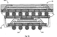
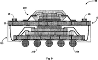
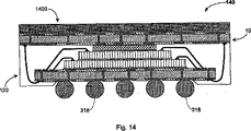
この発明は、第1のパッケージ基板のダイ取付側の上に実装され、第1のパッケージ基板のダイ取付側に電気的に接続された少なくとも1つのダイを有し、かつ、ダイの上に実装された第2の基板を有する半導体パッケージに向けられる。ダイ取付側に対向する第1のパッケージ基板の側は、基板の「ランド」側と称されることができる。第2の基板は、第1のパッケージ基板のダイ取付側に面している第1の側と、第1のパッケージ基板のダイ取付側から離れる方に向いている、(第2の基板の「ランド」側と称されることができる)第2の側とを有する。したがって、基板の「ランド」側は互いに離れる方に向いている。第1のパッケージ基板および第2の基板のz相互接続は、第1のパッケージ基板および第2の基板を接続するワイヤボンドによるものである。
SUMMARY The present invention is mounted on the first package substrate die attach side, has at least one die electrically connected to the die attach side of the first package substrate, and, on the dialog Directed to a semiconductor package having a second substrate mounted thereon. The side of the first package substrate that faces the die attach side can be referred to as the “land” side of the substrate. The second substrate faces the first side facing the die attachment side of the first package substrate and the direction away from the die attachment side of the first package substrate. And a second side (which may be referred to as the “land” side). Therefore, the “land” sides of the substrate are oriented away from each other. The z interconnection of the first package substrate and the second substrate is by wirebond connecting the first package substrate and the second substrate.
概してこの発明に従うと、第2の基板の第2の側の少なくとも一部および第1のパッケージ基板のランド側の少なくとも一部の両方が露出するように第1のパッケージ基板および第2の基板はアセンブリ封止部により封止され、その結果、第2のレベルの相互接続および追加の構成要素との相互接続がなされ得る。 Generally According to the present invention, the second side of the second substrate at least a portion and the land side of the first package substrate of at least part both the first package substrate and the second so as to expose The substrate is sealed with an assembly seal so that a second level of interconnection and interconnection with additional components can be made.
いくつかの実施例では、ダイはワイヤボンドによって第1のパッケージ基板と電気的に接続され、これらの実施例では、第2の基板はスペーサによってダイの上に支持され、スペーサはワイヤループの高さを収容するために第2の基板の第1の側とダイの上部との間に十分な空間を与える。第2の基板は、ダイの上に実装された(たとえば「ダミー(dummy)」ダイなどの)スペーサによって支持される場合もあれば、第2の基板は第1のパッケージ基板の上に実装されたスペーサ(たとえばエポキシドットまたはピア)によって支持される場合もある。 In some embodiments, dialog is connected to the first package substrate and electrically by wire bonds, in these embodiments, the second substrate is supported on the dialog by the space Sa, spacers Provides sufficient space between the first side of the second substrate and the top of the die to accommodate the height of the wire loop. The second substrate may or may therefore be supported implemented (e.g. "dummy (dummy)" die, etc.) space Sa on the dialog, the second substrate on the first package substrate sometimes supported by implemented space Sa (for example epoxy dots or peer).
第1のパッケージ基板と第2の基板との間のz相互接続は、第1のパッケージ基板のランド側の縁のエリアにおけるワイヤボンド箇所と、第2の基板の第1の側の縁のエリアにおける、周辺に位置するワイヤボンド箇所との間のワイヤボンドによる。 The z-interconnect between the first package substrate and the second substrate is comprised of wire bond locations in the land side edge area of the first package substrate and the first side edge area of the second substrate. In this case, the wire bond between the wire bond points located in the periphery is.
この発明の1つの一般的な局面に従うと、第2の基板は、ワイヤボンドの全長を収容するために第1のパッケージ基板よりも大きい(すなわち、幅が広いもしくは長い、または幅が広くかつ長い)。アセンブリ封止部は、スペーサが接触していない第2の基板の第1の側のいかなるエリアも覆い、z相互接続ワイヤボンドおよびワイヤループ、第1のパッケージ基板の端縁、ならびに第1のパッケージ基板のランド側の縁のエリアを密閉する。したがって、第2の基板のランド側および縁のエリアの内側に位置する第1のパッケージ基板のランド側のエリアは両方、露出したままである。 According to one general aspect of the invention, the second substrate is larger (ie, wider or longer, or wider and longer than the first package substrate to accommodate the entire length of wire bonds. ). Assembly sealing portion, also covers any area of the first side of the second substrate space Sa is not in contact, z-interconnect wire bonds and wire loops, the first package substrate edge, and the first Seal the land edge area of the package substrate . Therefore, both the land side of the first substrate and the land side area of the first package substrate located inside the edge area remain exposed.
この発明の別の一般的な局面に従うと、第1のパッケージ基板は、ワイヤボンドの全長を収容するために第2の基板よりも大きい(すなわち、幅が広いもしくは長い、または幅が広くかつ長い)。この局面に従うアセンブリでは、アセンブリ封止部は、スペーサが接触していない第2の基板の第1の側のいかなるエリアも覆い、z相互接続ワイヤボンドおよびワイヤループ、第2の基板の端縁、ならびに第2の基板のランド側の縁のエリアを密閉する。したがって、第1のパッケージ基板のランド側および縁のエリアの内側に位置する第2の基板のランド側のエリアは両方、露出したままである。 According to another general aspect of the invention, the first package substrate is greater than the second base plate to accommodate the entire length of the wire bonds (i.e., a wide or long width, or width and widely long). In the assembly according to this aspect, the assembly sealing portion, also covers any area of the first side of the second substrate space Sa is not in contact, z-interconnect wire bonds and wire loops, edges of the second substrate , As well as the area of the land side edge of the second substrate . Therefore, both the land side of the first package substrate and the land side area of the second substrate located inside the edge area remain exposed.
この発明の一局面に従うと、ダイおよび第1のパッケージ基板は、第1のパッケージ基板とのダイの電気的な相互接続部とともに、パッケージサブアセンブリを構成する。いくつかの実施例では、第1のパッケージ基板はボールグリッドアレイ基板を含み、マザーボードなどの下にある回路とのパッケージの第2のレベルの相互接続は、第1のパッケージ基板のランド側の露出した部分または第2の基板の露出したランド側におけるはんだボール相互接続(または他の第2のレベルの相互接続)によってなされるか、または、第1のパッケージ基板が第2の基板よりも大きい場合には、マザーボードなどの下にある回路とのパッケージの第2のレベルの相互接続は、第1のパッケージ基板のランド側におけるはんだボール相互接続によってなされる。 According to one aspect of the invention, dialog and the first package substrate, with electrical interconnections of the die and the first package substrate, constituting a package subassembly. In some embodiments, the first package substrate includes a ball grid array substrate, and the second level interconnection of the package with circuitry underneath, such as a motherboard, is exposed on the land side of the first package substrate. or it is made by solder ball interconnection (or interconnect other second level) in the part or exposed land side of the second substrate, or the first package board than the second substrate In the larger case, the second level interconnection of the package with the underlying circuitry, such as the motherboard, is made by solder ball interconnection on the land side of the first package substrate.
いくつかの実施例では、パッケージサブアセンブリは、第1のパッケージ基板の上に付着され、第1のパッケージ基板と電気的に相互接続されたダイを含む。いくつかの実施例では、パッケージにおけるダイはワイヤボンディングによって第1のパッケージ基板と相互接続され、またはパッケージにおけるダイはフリップチップ相互接続によって第1のパッケージ基板と相互接続される。 In some embodiments, Pas Tsu cage subassembly is deposited on the first package substrate, comprising a first package substrate and electrically interconnected dialog. In some embodiments, the dies in the package are interconnected with the first package substrate by wire bonding, or the dies in the package are interconnected with the first package substrate by flip chip interconnection.
好ましい実施例では、パッケージのパッケージサブアセンブリ側は第2のレベルの相互接続側である。すなわち、(たとえばマザーボードなどの)下にある回路とのパッケージの第2のレベルの相互接続は、第1のパッケージ基板のランド側の露出したエリア上のランドにおけるはんだボール(または電気的な接続の他の手段)による。したがって、第2の基板の露出したランド側は、アセンブリの上に積層され得る追加の構成要素と相互接続するのに利用可能である。さらなる局面では、次いで、この発明は、パッケージの一方の側において露出した第2の基板と、アセンブリの対向する側において露出した第1のパッケージ基板の一部との両方を有し、かつ、第1のパッケージ基板の露出した部分に形成された第2のレベルの相互接続部と、露出した第2のパッケージ基板における1つ以上の追加の構成要素との相互接続部とを含む半導体パッケージを特徴としている。いくつかの実施例では、追加の構成要素は、積層ダイボールグリッドアレイ(ball grid array)(BGA)であり得るBGAパッケージ、または積層ダイLGAであり得る追加のLGA、または積層ダイ・クアッド・フラット・パッケージ(stacked die quad flat package)(SD QFP)であり得るクアッド・フラット・パッケージ(QFP)、または積層ダイ・クアッド・フラット・パッケージ(SD QFN)であり得るクアッド・フラット・ノンリード(quad flat nonleaded)(QFN)パッケージまたはリードフレームチップスケールパッケージ(lead frame chip scale package)(LFCSP)、またはオーバーモールドされ得るワイヤボンドダイ(もしくはワイヤボンドダイの層)、またはフリップチップダイ、または光センサパッケージ、またはマイクロ・エレクトロ・メカニカルセンサ(micro-electro-mechanical sensor)(MEMS)パッケージのうち1つ以上を含み、追加の構成要素は1つ以上の受動素子をさらに含んでいてもよい。いくつかの実施例では、ヒートスプレッダが第2の基板の露出したランド側の上に実装される。 In the preferred embodiment, the package subassembly side of the package is the second level interconnect side. That is, the second level interconnection of the package with the underlying circuitry (such as a motherboard, for example) is a solder ball (or electrical connection of the land on the exposed area on the land side of the first package substrate). By other means). Thus, the exposed land side of the second substrate can be used to interconnect additional components that can be stacked on top of the assembly. In a further aspect, the invention then comprises both a second substrate exposed on one side of the package and a portion of the first package substrate exposed on the opposite side of the assembly, and the first A semiconductor package including a second level interconnect formed in an exposed portion of one package substrate and an interconnect with one or more additional components in the exposed second package substrate. It is said. In some embodiments, the additional component is a BGA package that can be a stacked die ball grid array (BGA), or an additional LGA that can be a stacked die LGA, or a stacked die quad flat. A quad flat package (QFP), which can be a stacked die quad flat package (SD QFP), or a quad flat nonleaded, which can be a stacked die quad flat package (SD QFN) ) (QFN) package or lead frame chip scale package (LFCSP), or wirebond die (or layer of wirebond die) that can be overmolded, or flip chip die, or photosensor package, or Microphone Electro include one or more of the mechanical sensor (micro-electro-mechanical sensor) (MEMS) package, additional components may further comprise one or more passive elements. In some embodiments, a heat spreader is mounted on the exposed land side of the second substrate.
この発明の別の局面に従うと、半導体アセンブリを作るための方法は、好ましくはボールグリッドアレイ(BGA)またはランドグリッドアレイ(land grid array)(LGA)基板のストリップのようなボールグリッドアレイまたはランドグリッドアレイ基板を設けるステップと、BGAまたはLGA基板の上にダイおよび相互接続部を実装して、パッケージサブアセンブリを形成するステップと、たとえばダイの上に実装されかつ表面上に
接着剤を備えるスペーサのようなもしくは第1のパッケージ基板の上に実装される接着性スペーサのようなスペーサまたはスペーサアセンブリをパッケージサブアセンブリの上に実装するステップと、スペーサ上の接着剤の上または接着性スペーサの上に第2の基板を実装するステップと、接着剤または接着性スペーサを硬化させるステップと、プラズマ洗浄を行なうステップと、ワイヤボンディングを行なって、第2の基板の第1の側と第1のパッケージ基板のランド側との間にz相互接続部を形成するステップと、プラズマ洗浄を行なうステップと、モールディング操作を行なって、基板の第1の側、z相互接続ワイヤボンドおよびワイヤループ、第1のパッケージ基板の端縁、ならびに第1のパッケージ基板のランド側の縁のエリアを密閉し、第2の基板の第2の(「ランド」)側および縁のエリア内に位置する第1のパッケージ基板のランド側のエリアを露出したままにするステップと、第2のレベルの相互接続はんだボールを第1のパッケージ基板の露出したエリア上の箇所に取付けるステップと、(第2の基板がストリップまたはアレイ状に設けられた場合には)鋸で切り分けて、パッケージを完成させるステップとを含む。
According to another aspect of the invention, a method for making a semiconductor assembly is preferably a ball grid array or land grid, such as a strip of a ball grid array (BGA) or land grid array (LGA) substrate. comprising the steps of providing an array substrate, by mounting the die and interconnects on a BGA or LGA substrate, forming a package sub-assembly, the example is mounted on the dialog and on the surface of the adhesive Mounting a spacer or spacer assembly, such as a spacer or an adhesive spacer mounted on a first package substrate, on a package subassembly, and on the adhesive on the spacer or of the adhesive spacer Mounting a second substrate thereon, and adhesive or contact Forming a z-interconnect between the first side of the second substrate and the land side of the first package substrate by curing the conductive spacer, performing the plasma cleaning, and performing wire bonding. Performing a plasma cleaning step and a molding operation to form a first side of the substrate, z-interconnect wire bonds and wire loops, an edge of the first package substrate, and a land side of the first package substrate Sealing the edge area of the second substrate, leaving the second (“land”) side of the second substrate and the land side area of the first package substrate located within the edge area exposed; Attaching a two level interconnect solder ball to a location on the exposed area of the first package substrate; If provided in Lee shape) isolate a saw, and a step to complete the package.
いくつかの実施例では、上記方法はさらに、第2の基板の露出したランド側において、追加の構成要素を付着させ、追加の構成要素を電気的に接続するステップを含む。追加の構成要素は、積層パッケージアセンブリを製造する際にさらなるステップとしてアセンブリの上に実装される可能性もあれば、追加の構成要素は最終的な製品組立フロアにおいてアセンブリの上に実装される可能性もある。 In some embodiments, the method further includes depositing additional components and electrically connecting the additional components on the exposed land side of the second substrate. Additional components may be mounted on the assembly as an additional step in manufacturing a stacked package assembly, or additional components may be mounted on the assembly on the final product assembly floor There is also sex.
この発明に従うパッケージでは、第2の基板は、z相互接続のために第1の側において露出したワイヤボンド箇所ならびにパッケージの検査のためにおよび/または追加の構成要素の相互接続のためにランド側において露出した箇所を有する限り、さまざまな基板のうちいずれも含み得る。追加の構成要素を有するモジュールまたはアセンブリはさまざまなLGAパッケージのうちいずれも含み得る。このアセンブリはワイヤボンドパッケージおよび/またはフリップチップパッケージを含み得る。このアセンブリはアセンブリの中またはアセンブリ上の1つ以上のヒートスプレッダによって可能になる熱強化特徴を含み得る。このアセンブリは、積層したまたは並んだ2つ以上のダイをパッケージの中に有する1つ以上のBGAおよび/またはLGAを含み得る。このアセンブリは1つ以上のパッケージのための電磁シールドを含み得る。このアセンブリは、z相互接続パッドが第1のパッケージ基板および第2の基板の周辺エリア上でのボンディングに利用可能であるという条件で、任意の基板、すなわち積層板基板または積上げ基板または可撓性基板またはセラミック基板を含み得る。 In the package according to the invention, the second substrate is exposed on the first side for z-interconnect and the land side for inspection of the package and / or for interconnection of additional components. Any of a variety of substrates can be included as long as they have exposed locations at. A module or assembly with additional components may include any of a variety of LGA packages. The assembly may include a wire bond package and / or a flip chip package. The assembly may include thermal enhancement features enabled by one or more heat spreaders in or on the assembly. The assembly may include one or more BGAs and / or LGAs with two or more dies stacked or side-by-side in the package. The assembly can include electromagnetic shields for one or more packages. This assembly can be used on any substrate, i.e. a laminated or stacked substrate or flexible, provided that the z-interconnect pads are available for bonding on the peripheral areas of the first package substrate and the second substrate. A substrate or a ceramic substrate may be included.
この発明は、優れた製造可能性、高い設計の柔軟性および低コストをもたらして、プロファイルが低くかつ設置面積が小さな積層パッケージモジュールを生み出す。 The present invention provides excellent manufacturability, high design flexibility and low cost to produce a stacked package module with a low profile and a small footprint.
パッケージおよびモジュールまたはアセンブリ、ならびにダイおよび基板およびダイ積層プロセスおよび相互接続プロセスは業界内で標準的なものであり、最低コストおよび最大幅の可用性の選択をもたらす。これは、積層されるべき構成要素の選択、したがってアセンブリに一体化できる機能の種類に大幅な柔軟性をもたらす。 Packages and modules or assemblies, as well as die and substrate and die stacking and interconnect processes are standard within the industry, resulting in a choice of lowest cost and maximum width availability. This provides great flexibility in the choice of components to be stacked and thus in the types of functions that can be integrated into the assembly.
典型的な単一のワイヤボンドダイサブアセンブリの厚さは、(接着剤を含む)ダイの上のスペーサと合わせて、約0.8mmである。この発明の構造に従ってパッケージサブアセンブリの上に第2の基板を積層することによって、追加の構成要素(パッケージまたはダイまたは受動素子)を積層するための、広範囲にわたって有用なプラットフォームが設けられる。この発明に従うアセンブリの設置面積は、層の最大チップサイズに応じて決定されることができる。ワイヤボンドz相互接続は概して、基板の金属端縁が短絡することなくワイヤを収容するために、パッケージサブアセンブリ基板が第2の基板よりも約0.5mmから1.0mmだけ小さいことが必要である。選択されたパッケージサブアセンブリが上部基板よりも大幅に小さい場合には、ワイヤボンディングは少なくとも8mm以上までの大きさの違いに対処できる。したがって、所与の選択されたパッケージサブアセンブリでは、これによって、設置面積が第1のパッケージよりも大幅に大きい上部基板を選択することが可能になる。これは、アセンブリの上に積層されるべき追加の構成要素を選択するための大幅な柔軟性を設計者に与える。 The thickness of a typical single wirebond die subassembly is about 0.8 mm, combined with the spacers on the die (including the adhesive). Laminating a second substrate over a package subassembly in accordance with the structure of the present invention provides a widely useful platform for laminating additional components (packages or dies or passive elements). The footprint of the assembly according to the invention can be determined according to the maximum chip size of the layer. The wire bond z interconnect generally requires that the package subassembly substrate be about 0.5 mm to 1.0 mm smaller than the second substrate in order to accommodate the wires without the metal edges of the substrate short circuited. is there. If the selected package subassembly is significantly smaller than the top substrate, wire bonding can handle size differences up to at least 8 mm. Thus, for a given selected package subassembly, this allows the selection of an upper substrate that has a significantly larger footprint than the first package. This gives the designer great flexibility to select additional components to be stacked on the assembly.
この発明に従うパッケージおよびモジュールまたはアセンブリは、コンピュータ、電気通信機器ならびに民生用および産業用電子装置を構築するために使用されることができる。 Packages and modules or assemblies according to the invention can be used to construct computers, telecommunications equipment and consumer and industrial electronic devices.
詳細な説明
ここで、この発明の代替的な実施例を示す図面を参照することによってさらに詳細にこの発明について記載する。この発明の特徴ならびに他の特徴および構造との関係を示す図面は概略的なものであり、一定の比例に応じているわけではない。説明の明確さを向上させるために、この発明の実施例を示す図面では、他の図に示されている要素に対応する要素はすべてが特に名称を変更されるわけではないが、すべての図面においてすべて容易に識別可能である。
DETAILED DESCRIPTION The present invention will now be described in further detail by reference to the drawings which show alternative embodiments of the invention. The drawings showing the features of the invention and the relationships with other features and structures are schematic and do not correspond to a certain proportion. In order to improve the clarity of explanation, in the drawings showing the embodiments of the present invention, not all of the elements corresponding to the elements shown in other drawings are renamed in particular. Are all easily identifiable.
本明細書におけるいくつかの箇所では、「水平な(horizontal)」、「垂直な(vertical)」、「上に(on)」、「真上に(over)」、「下に(under)」、「上方に(above)」、「下方に(below)」、「最上部(top)」、「底部(bottom)」、「上部(upper)」、「下部(lower)」などの相対的な向きの用語は、図面に示す特徴の相対的な向きを基準にして使用されることができる。理解されるように、この発明に従うさまざまなアセンブリは、使用時にまたは加工中にいずれの向きに保持されてもよい。 In several places herein, “horizontal”, “vertical”, “on”, “over”, “under” , “Above”, “below”, “top”, “bottom”, “upper”, “lower”, etc. Orientation terms can be used in reference to the relative orientation of features shown in the drawings. As will be appreciated, the various assemblies according to the present invention may be held in any orientation during use or during processing.
上記または下記において本明細書で参照されるすべての特許および特許出願は、引用によって援用される。 All patents and patent applications referred to herein above or below are incorporated by reference.
ここで図1を参照して、半導体パッケージアセンブリの実施例を概略的な断面図で概して1で示し、この半導体パッケージアセンブリは、第1の(図1では「底部」)パッケージサブアセンブリと、第1のパッケージサブアセンブリの上に積層した第2の(図1では「上部」)基板とを含み、パッケージおよび第2の基板はこの発明の局面に従ってワイヤボンディングによって相互接続される。図1に示す実施例では、底部パッケージサブアセンブリ100は、少なくとも1つの金属層を有する第1の(底部)パッケージ基板112の上に取付けられたダイ114を含む。たとえば2〜6つの金属層を有する積層板、または4〜8つの金属層を有する積上げ基板、または1〜2つの金属層を有する可撓性のポリイミドテープ、またはセラミック多層基板を含むさまざまな基板タイプのいずれが使用されてもよい。図1に一例として示す第1のパッケージ基板112は2つの金属層121、123を有し、各々は適切な回路を設けるためにパターニングされ、ビア122を介して接続される。ダイは、従来から、図1に113で示す、典型的にはダイ取付エポキシと称される接着剤を使用して基板の表面に取付けられ、図1における構成では、ダイが上に取付けられる基板の側(「ダイ取付」側)は「上」側と称されることができ、その側の金属層は「上部」金属層と称されることができるが、ダイ取付側は使用時に任意の特定の向きを有する必要はない。
Referring now to FIG. 1, an example of a semiconductor package assembly is shown generally at 1 in a schematic cross-sectional view, which includes a first (“bottom” in FIG. 1) package subassembly, And a second ("upper" in FIG. 1) substrate stacked on top of one package subassembly, the package and the second substrate being interconnected by wire bonding in accordance with aspects of the invention. In the embodiment shown in FIG. 1, the
図1の底部パッケージサブアセンブリでは、ダイは基板の上部金属層上のワイヤボンド箇所の上にワイヤボンドされて、電気的な接続部を確立する。 In the bottom package subassembly of FIG. 1, the die is wire bonded over the wire bond points on the top metal layer of the substrate to establish an electrical connection.
たとえばマザーボード(図には図示せず)の下にある回路にアセンブリを第2のレベルで相互接続するために、ボンディングパッド119が基板112の下部金属層123上に設けられる。はんだマスク115、127が金属層121、123の上にパターニングされて、電気的に接続するためのボンディング箇所における下にある金属、たとえばワイヤボンド116およびはんだボール318をボンディングするためのワイヤボンド箇所ならびにボンディングパッドを露出させる。
For example,
依然として図1を参照して、第1の側および第2の側を有する第2の(「上部」)基板10は、基板誘電体12と少なくとも1つの金属層とを含む。さまざまな基板タイプのいずれが使用されてもよい。図1に一例として示す基板10は2つの金属層21、23を有し、各々は適切な回路を設けるためにパターニングされ、ビア22を介して接続される。第1のパッケージサブアセンブリに面している第2の基板の側は第1の側と称され、対向する側−第2の側または「ランド側」−は第1のパッケージサブアセンブリから離れる方
に向いている。
Still referring to FIG. 1, a second (“upper”)
図1の実施例における第2の基板10では、はんだマスク15、27が金属層21、23の上にパターニングされて、電気的に接続するためのボンディング箇所における下にある金属、たとえばワイヤボンド118をボンディングするためのワイヤボンド箇所を露出させる。
In the
図1の例における第2の基板は、第1のパッケージ基板のダイ側に実装されたドットまたはピア13によって支持されている。支持体13はたとえば充填エポキシバンプであってもよく、充填エポキシバンプは、ダイ114の表面129の上にワイヤボンド116のループの高さを収容するのに十分に大きな距離をおいて第2の基板をパッケージダイの上に保持するのに十分な高さを第1のパッケージ基板の上に有する。
The second substrate in the example of FIG. 1 is supported by dots or peers 13 mounted on the die side of the first package substrate. The
第2の(「上部」)基板10および第1の(「底部」)パッケージサブアセンブリ100のz相互接続は、上部基板の下向きに向いている金属層(金属層21)上のトレースを、底部パッケージ基板の下部金属層123上のトレースと接続するワイヤボンド118を介してなされる。一端において、各ワイヤボンド118は、上部基板12の金属層21上のパッドの下向きに向いている面に電気的に接続され、他端において、各ワイヤボンドは、底部パッケージ基板112の下部金属層123上のパッドの下面に接続される。ワイヤボンドは、たとえば引用によって本明細書に援用される米国特許第5,226,582号に記載されるものなどの、当該技術分野において周知の任意のワイヤボンディング技術によって形成されることができる。基板とパッケージとのz相互接続ワイヤボンドは、上部基板の下部金属層上のパッドの表面上にビードまたはバンプを形成し、次いで底部基板の下部金属層上のパッドの方にワイヤを延伸し、底部基板の下部金属層上のパッドの上にワイヤを溶融することによって作られたものとして図1に一例として示す。理解されるように、ワイヤボンドは逆方向に、すなわち、底部基板の下部金属層上のパッドの下面上にビードまたはバンプを形成し、次いで上部基板の金属層上のパッドの方にワイヤを延伸し、上部基板の金属層上のパッドの上にワイヤを溶融することによって、作られることができる。理解されるように、基板とパッケージとのz相互接続のためのワイヤボンディング戦略の選択は、積層基板の縁および積層基板上のボンディング面の幾何学的配置に従って決定されることになる。さらに、理解されるように、従来のワイヤボンディング機器では、ワイヤボンドキャピラリは上向きに向いたボンドパッドの上に下向きに突き当たり、したがって、少なくともワイヤボンディング手順に関してはこの発明に従うとアセンブリを反転させることになる。
The z-interconnect of the second (“top”)
上で指摘したように、図1と同様の実施例では、上部基板は、上部基板が上に実装される第1のパッケージサブアセンブリの設置面積よりも大きく、ワイヤボンド118のためにボンドパッドが露出するエリアを上部基板の第1の側の周辺に残す。上部基板はパンチまたは鋸で切り分けられる。
As pointed out above, in an embodiment similar to FIG. 1, the top substrate is larger than the footprint of the first package subassembly on which the top substrate is mounted, and the bond pads for
底部パッケージ基板のダイ取付側の上部金属層におけるボンドパッドはワイヤボンドによってダイに接続され、上部金属層は、基板のダイ取付側へのビアを介して底部パッケージ基板のランド側における下部金属層に接続され、底部パッケージ基板のランド側における下部金属層はパターニングされて、z相互接続ワイヤ118と接続するための、周辺に配置されたボンドパッドを設ける。
The bond pad on the upper metal layer on the die mounting side of the bottom package substrate is connected to the die by wire bonding, and the upper metal layer is connected to the lower metal layer on the land side of the bottom package substrate via vias to the die mounting side of the substrate. Connected, the bottom metal layer on the land side of the bottom package substrate is patterned to provide a peripherally disposed bond pad for connection to the
この発明に従う構造によって、モジュールまたはアセンブリに組立てる前にパッケージを予備検査することが可能であり、組立に先立って不適合なパッケージを不合格にすることが可能であり、それによって最終的なモジュール検査の歩留まりを確実に高くする。 With the structure according to the invention, it is possible to pre-inspect the package prior to assembly into a module or assembly, and to reject non-conforming packages prior to assembly, thereby allowing final module inspection. Make sure to increase the yield.
図1の実施例では、それぞれの基板上のz相互接続パッドは、基板の縁の近くの金属層上に配置される。z相互接続パッドの位置および順序は概して、パッケージを積層するときに上部パッケージ基板上のz相互接続パッドが底部パッケージ上の対応するz相互接続パッドのほぼ上に横たわるように配置される。好都合なことに、上部基板10の基板設置面積は底部パッケージ100の基板設置面積よりも大きく、基板の金属層の端縁が電気的に短絡することなくワイヤボンドのための間隙が可能になる。
In the embodiment of FIG. 1, the z-interconnect pads on each substrate are placed on a metal layer near the edge of the substrate. The location and order of the z interconnect pads is generally arranged so that when stacking the packages, the z interconnect pads on the top package substrate lie substantially over the corresponding z interconnect pads on the bottom package. Conveniently, the substrate footprint of the
積層した第1のパッケージおよび第2の基板を接続するz相互接続ワイヤボンドが一旦形成されると、アセンブリ封止部107が形成されて、z相互接続ワイヤボンドを密閉および保護し、完成したアセンブリに機械的な整合性を与える。アセンブリ封止部107は、支持体が接触していない第2の基板の下向きに向いている第1の側のエリアを覆い、z相互接続ワイヤボンドおよびワイヤループ、ならびに底部パッケージの垂直壁および端縁を密閉し、ワイヤループおよびワイヤボンドが接続されるワイヤボンドパッドを含む底部パッケージ基板のランド側の縁のエリアを覆う。これによって、第2のレベルの相互接続のために、底部パッケージ基板のランド側のエリアが露出したままになる。別の言い方をすれば、第1のパッケージ側のアセンブリ封止部にキャビティが形成され、第2のパッケージ基板のランド側の内側エリアを露出した(封止されない)ままにする。図3を参照して、はんだボール318が基板の下部金属層上のボンディングパッド119の上にリフローされて、たとえばコンピュータなどの最終製品のマザーボード(図には図示せず)の下にある回路への相互接続をもたらす。以下にさらに詳細に記載するように、追加のパッケージまたはダイを第2のパッケージ基板のランド側の上に実装でき、第2のパッケージ基板のランド側と電気的に接続させることができる。
Once the z-interconnect wire bond connecting the stacked first package and the second substrate is formed, an
図1および図3に一例として示すように、パッケージは鋸で切り分けられてもよく、代替的には、モジュールは鋸で切り分けられるのではなく個々にモールドされてもよい。 As shown by way of example in FIGS. 1 and 3, the packages may be sawed and, alternatively, the modules may be molded individually rather than sawed.
理解され得るように、第1のパッケージサブアセンブリは、第1のパッケージ基板へのダイのワイヤボンディング相互接続部ではなくフリップチップ相互接続部を有していてもよい。いくつかの実施例では、第2の基板用の支持体は、第1のパッケージサブアセンブリダイの上に実装されたスペーサであり得る。 As can be appreciated, the first package subassembly may have flip chip interconnects rather than wire bonding interconnects of the die to the first package substrate. In some embodiments, the support for the second substrate can be a spacer mounted on the first package subassembly die.
第1のパッケージは積層ダイパッケージであってもよい。図2は、図2の例では底部パッケージサブアセンブリが、2つのワイヤボンドされたダイを有する積層ダイをパッケージ基板の上に実装させ、パッケージ基板と電気的に相互接続させること以外は、概して図1と同様の半導体パッケージアセンブリ2を一例として示す。ここで図2を参照して、パッケージサブアセンブリ120では、第1のダイ114は接着剤を使用して基板112の(図では上向きに向いている)ダイ取付側に取付けられ、第2のダイ144は接着剤を使用して第1のダイ114の(上向きに向いている)ダイ取付側に取付けられる。第1のダイ114および第2のダイ144は、ワイヤボンド116、146によって、上部金属層121におけるボンド箇所にそれぞれに電気的に接続される。
The first package may be a stacked die package. FIG. 2 is a schematic diagram, except that the bottom package subassembly in the example of FIG. 2 has a stacked die having two wirebonded dies mounted on the package substrate and electrically interconnected with the package substrate. The semiconductor package assembly 2 similar to 1 is shown as an example. Referring now to FIG. 2, in the
図2の例では、第2の基板10は図1の第2の基板10と実質的に同一である。パッケージアセンブリ2では、(たとえば「ダミー」ダイまたはシリコンもしくはガラスチップであり得る)スペーサ14が接着剤213を使用して最も上の積層ダイ144の上に実装され、第2の基板10はスペーサ14の表面の接着剤215を使用してスペーサ14の上に付着される。したがって、第2の基板の下向きに向いている面19は接着剤215の上に載っており、スペーサ14の厚さならびに接着剤213および215の厚さは、ワイヤボンド146のループの高さを収容するのに十分に大きいものであるように選択される。
In the example of FIG. 2, the
他のスペーサまたはスペーサ構造物がこの発明に従って利用されてもよい。たとえば、
スペーサ14は、ダイ144の上向きに向いている面229と基板10の下向きに向いている面19との間に所望の分離をもたらすのに十分な直径を有するポリマー球で充填された硬化可能な接着剤からなる接着性スペーサであってもよい。
Other spacers or spacer structures may be utilized in accordance with the present invention. For example,
The
他の実施例では、第2のダイの設置面積が、ワイヤボンドと干渉することなく第1のダイの上に第2のダイを積層できないようなものである場合(たとえば第2のダイが第1のダイと同一の大きさであるか、または第1のダイよりも大きい場合)には、スペーサを第1のダイの上に実装でき、第2のダイをスペーサの上に実装できる。 In other embodiments, the second die footprint is such that the second die cannot be stacked on top of the first die without interfering with the wire bonds (eg, the second die is the second die). The spacer can be mounted on the first die and the second die can be mounted on the spacer (if it is the same size as one die or larger than the first die).
第1のパッケージサブアセンブリにおける第1のダイは、第1のパッケージ基板へのダイのワイヤボンディング相互接続部ではなくフリップチップ相互接続部を有していてもよく、第2のダイは、概して上述したように、第1の(フリップチップ)ダイの(上向きに向いている)裏面の上に実装されることができ、第1のパッケージ基板の上部金属層におけるボンドパッドにワイヤボンドされることができる。 The first die in the first package subassembly may have flip chip interconnects rather than wire bond interconnects of the die to the first package substrate, and the second die is generally described above. As such, it can be mounted on the back (facing upward) side of the first (flip chip) die and can be wire bonded to bond pads in the upper metal layer of the first package substrate. it can.
z相互接続ワイヤボンド218は、概して図1でz相互接続ワイヤボンド118について記載したように形成される。積層した第1のパッケージおよび第2の基板を接続するz相互接続ワイヤボンドが一旦形成されると、アセンブリ封止部207が形成されて、z相互接続ワイヤボンドを密閉および保護し、完成したアセンブリに機械的な整合性を与える。アセンブリ封止部207は、第2の基板の下向きに向いている第1の側の縁のエリアを覆い、z相互接続ワイヤボンドおよびワイヤループ、ならびに底部パッケージの垂直壁および端縁を密閉し、ワイヤループおよびワイヤボンドが接続されるワイヤボンドパッドを含む底部パッケージ基板のランド側の縁のエリアを覆う。これによって、第2のレベルの相互接続のために、底部パッケージ基板のランド側のエリアが露出したままになる。図3に一例として示すように、はんだボール318が、露出した下部パッケージ基板の下部金属層上のボンディングパッド119の上にリフローされて、たとえばコンピュータなどの最終製品のマザーボード(図には図示せず)の下にある回路への相互接続をもたらす。
The z
代替的な実施例では、第2の基板の露出した側は第2のレベルの相互接続をもたらす。一例として、図4に示す実施例は、パッケージアセンブリをマザーボードなどの下にある回路に接続するために、第2のレベルの相互接続はんだボール418を金属層23上のパッド419の上に実装させる。このような実施例では、第1のパッケージ基板の露出した
部分は、パッケージ、ダイまたは受動素子などの追加の構成要素の積層に利用可能である。しかしながら、第1のパッケージ基板の露出した部分は第2のパッケージ基板よりもエリアが限られており、第1のパッケージ側に作られることができる相互接続部の数を制限する。さらに、第1のパッケージ基板のランド側の縁のエリアを覆うアセンブリモールディング207の一部は、ワイヤボンド218のループの高さ(および許容差)を収容するのに十分に厚くなければならない。典型的には、ワイヤループにおけるモールディングの厚さは約50μmから約200μmの範囲にある。ワイヤループの端部が第1のパッケージのランド側のパッドの上にステッチングされるように逆方向のワイヤボンディングが利用される場合には、ワイヤループの高さは実際にはわずか約35μmであってもよく、したがって、このような実施例ではわずか約100μmという縁のエリアの上のモールディングの厚さを達成できる。順方向のワイヤボンディングが利用される場合には、より大きなモールドの高さが必要になる。なぜなら、厚さが約1ミルのワイヤを形成する、現在利用可能なワイヤボンディング技術を使用するボール(またはバンプ)上のワイヤループの高さは、通常約100μm以上であるためである。
In an alternative embodiment, the exposed side of the second substrate provides a second level of interconnect. As an example, the embodiment shown in FIG. 4 allows second level
これは事実上、第1のパッケージ基板の露出した領域の周りの低い壁を引上げ、これは第1のパッケージ基板のランド側の上に積層され得る素子の寸法および構成を制限する可能性がある。第2のレベルの相互接続が第1のパッケージ基板のランド側の露出した領域
でなされる、たとえば図3に示す実施例によって、たとえば図7Bおよび図8Bに示すようにアセンブリの上にはるかに大きな追加の構成要素を積層することが可能になる。
This effectively raises the low walls around the exposed area of the first package substrate, which can limit the size and configuration of the elements that can be stacked on the land side of the first package substrate. . The second level interconnect is made in an exposed area on the land side of the first package substrate, for example, with the embodiment shown in FIG. 3, much larger above the assembly as shown, for example, in FIGS. 7B and 8B. Additional components can be stacked.
図5Aおよび図5Bは、図2において112で示した好適な第1のパッケージ基板のランド側およびダイ取付側をそれぞれに示す平面図の概略図である。図5Aを参照して、ランド側の表面の大半ははんだマスクによって覆われており、はんだマスクは、金属層上の箇所がはんだマスクの開口によって露呈している場合を除いて、下にあるパターニングされた金属層を覆い隠している。はんだマスクの開口によって、基板表面の中央領域に配列されたボールパッド(たとえば53)および基板の端縁52の近くの縁のエリアに配置されたボンドフィンガ(たとえば56)を含む、基板のランド側のパターニングされた金属層における箇所が露呈する。はんだマスクが覆い隠しているのは、ボールパッド53およびボンドフィンガ56をさまざまに接続するならびに/またはボールパッド53をビア(たとえば522)と接続する金属層におけるトレース(たとえば523)であり、ビアは、基板のランド側のパターニングされた金属層におけるトレースを、基板のダイ取付側のパターニングされた金属層におけるトレースと電気的に接続する。
5A and 5B are schematic plan views illustrating the land side and die attach side of the preferred first package substrate indicated at 112 in FIG. 2, respectively. Referring to FIG. 5A, most of the land-side surface is covered by a solder mask, and the solder mask is patterned underneath unless the metal layer is exposed by the opening of the solder mask. The metal layer is covered and hidden. The land side of the substrate including a ball pad (eg, 53) arranged in a central region of the substrate surface by a solder mask opening and a bond finger (eg, 56) disposed in an edge area near the
上述のように、アセンブリ封止部は、ボンドパッド56と、パッド56に形成されたワイヤループとを覆う。封止部は、基板のランド側において、図5Aに破線58によって示す縁のエリアに限定され、そのため、縁の封止部が境界となる第1のパッケージ基板のランド側の領域、すなわち破線58の範囲内の第1のパッケージ基板のランド側の領域は、アセンブリモールディングの形成後、露出したままにされる。したがって、ボールパッド53は、(たとえば図4に示すように)追加の素子の取付に利用可能であり、または(たとえば図3に示すように)下にある回路へのアセンブリのzレベルの相互接続に利用可能である。ボールパッド53はさらに、組立に先立ってパッケージを検査するため、または所望であれば、第2のレベルの相互接続はんだボールの実装に先立ってパッケージアセンブリを検査するための検査プローブ箇所として利用可能である。封止された縁のエリアの幅(図5AではMW)は、ボンドフィンガの長さ、ボンドフィンガへのトレースの長さおよび鋸の通り道の幅の合計によって決定される。さらに、(図5Aの破線58における)縁の内縁における基板表面上に何らかのモールド鋳ばりが現れる場合がある。基板がストリップまたはアレイ状の基板として設けられる場合、第1のパッケージを鋸で切り分ける間に端縁におけるいくらかの基板材料が失われて鋸の幅になる。典型的には、ボンドフィンガの長さは約250μmであり、フィンガトレースの長さは約50μmであり、モールド樹脂の流出のためのゆとりは約500μmであり得る。鋸は典型的には約50μmを費やす。
As described above, the assembly seal covers the
実際問題として、ボールパッド53の数および配置はボールの公称直径に依存する。なぜなら、ボールは崩壊したときに互いに接触してはならず、またはともに接近しすぎてはならないためである。さらに、実際問題として、ボールパッド53の大きさおよび近さは、トレースおよび特にはんだマスクの開口を製造する際の解像度の限界によって制限される。典型的な例では、ボールパッドは、直径が約280μmの概して円形であり、中心から中心までの距離が約500μmで正方形または長方形のアレイ状に配置される。(隣接するはんだマスクの開口の最も近い端縁間の距離は典型的には、中心から中心までの距離の約0.20倍以上である。)
ダイが取付けられた状態の第1のパッケージ基板のダイ取付側を図5Bに示す。第1のダイ114は、基板のダイ取付側の上に、活性側を上に向けて付着される。この例では、ダイは正方形を規定する4つの端縁を有する。ワイヤボンドパッド51は、ダイの4つの端縁の近くに列をなして配置される。基板のランド側と同様に、ダイ取付側の表面の大半は、特にボンドフィンガ(たとえば54)の列(この例では、ダイの各端縁に沿った1列)を含む、金属層上の箇所がはんだマスクの開口によって露呈している場合を除いて、はんだマスクによって覆われている。ワイヤ116は、ダイパッド51をボンドフィンガ5
4と接続する。はんだマスクが覆い隠しているのは、ボンドフィンガ54をビア(たとえば522)に接続する金属層におけるトレース(たとえば521)であり、ビアは、基板のダイ取付側のパターニングされた金属層におけるトレースを、ランド側のパターニングされた金属層におけるトレースと電気的に接続する。したがって、第1のパッケージダイは、ワイヤを介して第1のパッケージ基板のダイ取付側の金属層におけるトレースに接続され、ビアを介してランド側の金属層におけるz相互接続ワイヤボンドフィンガに接続される。z相互接続ワイヤは、第1のパッケージ基板のランド側のボンドフィンガを第2のパッケージ基板のダイ取付側のボンドフィンガに接続する。第2のダイ144の設置面積は破線544によって図5Bに示されている。スペーサ14の設置面積は図5Bに破線514によって示されている。代替的には、第2のダイの上に実装されたスペーサ14ではなく第1の基板上のスペーサ13が利用される場合、その位置はたとえば破線513によって一例として示されている。第2のダイおよびワイヤボンド146ならびにスペーサ14、または代替的にスペーサ13は、簡略化するために図5Bからは省略されている。
In practice, the number and placement of
FIG. 5B shows the die attachment side of the first package substrate with the die attached. The
4 is connected. Covered by the solder mask is a trace (eg, 521) in the metal layer that connects the bond finger 54 to the via (eg, 522), which is a trace in the patterned metal layer on the die attach side of the substrate. Electrically connect with traces in the patterned metal layer on the land side. Thus, the first package die is connected via wires to traces in the metal layer on the die mounting side of the first package substrate and via vias to z interconnect wire bond fingers in the land side metal layer. The The z interconnect wires connect the land-side bond fingers of the first package substrate to the die-attachment side bond fingers of the second package substrate. The footprint of the
図6Aおよび図6Bは、図1において10で示した好適な第2の基板の第2の側および第1の側をそれぞれに示す平面図の概略図である。図6Aを参照して、ランド側の表面の大半ははんだマスクによって覆われており、はんだマスクは、金属層上の箇所がはんだマスクの開口によって露呈している場合を除いて、下にあるパターニングされた金属層を覆い隠している。はんだマスクの開口によって、基板表面の中央領域に配列されたボールパッド(たとえば63)を含む、基板のランド側のパターニングされた金属層における箇所が露呈する。はんだマスクが覆い隠しているのは、ボールパッド63をビア(たとえば622)に接続する金属層におけるトレース(たとえば623)であり、ビアは、基板のランド側のパターニングされた金属層におけるトレースを、基板の第1の側のパターニングされた金属層におけるトレースと電気的に接続する。
6A and 6B are schematic views in plan view showing the second side and the first side, respectively, of the preferred second substrate shown at 10 in FIG. Referring to FIG. 6A, most of the land-side surface is covered by a solder mask, and the solder mask is patterned underneath unless the metal layer is exposed by an opening in the solder mask. The metal layer is covered and hidden. The openings in the solder mask expose locations in the patterned metal layer on the land side of the substrate, including ball pads (eg 63) arranged in the central region of the substrate surface. Covered by the solder mask is a trace (eg, 623) in the metal layer that connects the
上述のように、第2の基板のランド側は、アセンブリ封止後、完全に露出したままにされる。したがって、図6Aにおける第2の基板の図は実質的にアセンブリの表面の図である。したがって、ボールパッド63は、(たとえば図4に示すように)下にある回路へのアセンブリの第2のレベルの相互接続に利用可能であり、またはより好ましくは、(たとえば図3に示すように)追加の素子の取付に利用可能である。ボールパッド63はさらに、組立に先立ってパッケージを検査するため、および所望であれば、第2のレベルの相互接続はんだボールの実装に先立ってパッケージアセンブリを検査するための検査プローブ箇所として利用可能である。
As described above, the land side of the second substrate remains fully exposed after assembly sealing. Thus, the view of the second substrate in FIG. 6A is substantially a view of the surface of the assembly. Accordingly, the
任意に、および好ましくはいくつかの適用例では、従来の検査ソケットを使用したアセンブリの検査を容易にするために第2の基板のランド側のボール取付パッドが利用されてもよい。このようなアセンブリの検査は、たとえば上部基板として第2の基板を取付けた後ではあるが、アセンブリモールディング全体を形成することに先立って、またはz相互接続ワイヤボンディングに先立って行なわれることができる。この発明の構造物に従って容易になる、製造時のさまざまな段階のうちいずれかでの検査は、仕様を満たさない構成要素をさらに加工する可能性を大幅に低減できる。 Optionally, and preferably in some applications, a ball mounting pad on the land side of the second substrate may be utilized to facilitate inspection of the assembly using a conventional inspection socket. Inspection of such an assembly can be performed prior to forming the entire assembly molding, or prior to z-interconnect wire bonding, for example, after attaching a second substrate as the top substrate. Inspection at any of the various stages during manufacture, facilitated according to the structure of the present invention, can greatly reduce the possibility of further processing components that do not meet specifications.
第2の基板の第1の側を図6Bに示す。第2の基板のランド側と同様に、第1の側の表面の大半は、特に基板の端縁62の近くの縁のエリアに配置されたz相互接続ボンドフィンガ(たとえば66)を含む、金属層上の箇所がはんだマスクの開口によって露呈している場合を除いて、はんだマスクによって覆われている。はんだマスクが覆い隠しているのは、ビア(たとえば622)をz相互接続ボンドフィンガ66に接続する金属層におけるトレース(たとえば621)であり、ビアは、基板の第1の側のパターニングされた金属層におけるトレースを、ランド側のパターニングされた金属層におけるトレースと電気的に接続する。
The first side of the second substrate is shown in FIG. 6B. Similar to the land side of the second substrate, the majority of the surface on the first side includes a z-interconnect bond finger (eg, 66) disposed particularly in the edge area near the edge 62 of the substrate. Except where the location on the layer is exposed by the opening of the solder mask, it is covered by the solder mask. Covered by the solder mask is a trace (eg, 621) in the metal layer that connects the via (eg, 622) to the z-
第2の基板のz相互接続パッド(ボンドフィンガ)66は、第2のパッケージ基板12の第1の側の縁に位置する金属層の領域をパターニングすることによって形成される。縁は第1の基板112の設置面積を超えて延在する。この設置面積は図6Bに破線68によって示されている。この縁の幅は約1mm未満である可能性があり、ワイヤボンディングのための十分な間隙を与えるために、縁の幅は好ましくは約0.2mmを上回っていてもよい。名目上、いくつかの実施例では、縁は約0.5mmである。第2の基板の下向きに向いている第1の側のスペーサ14の設置面積は図6Bに破線614によって示されており、または代替的には、第2の基板の下向きに向いている第1の側のスペーサ13の接触ポイントはたとえば図6Bに破線613によって示されている。
The second substrate z-interconnect pads (bond fingers) 66 are formed by patterning a region of the metal layer located at the first side edge of the
上述のように、パッケージの相互接続がアセンブリの上に積層した追加の素子に対してなされるか、または下にある基板に対してなされる(第2のレベルの相互接続)場合には、第2の基板の第1の側におけるz相互接続ボンドフィンガは、第1のパッケージ基板の第1の側の金属層におけるトレースによって、ビアを介してトレースおよびランド側の金属層におけるz相互接続ワイヤボンドフィンガに接続される。z相互接続ワイヤは、第2の基板の第1の側のボンドフィンガを第1のパッケージ基板のランド側のボンドフィンガに接続し、パッケージアセンブリの相互接続が下にある基板に対してなされる(第2のレベルの相互接続)か、またはアセンブリの上に積層した追加の素子に対してなされる場合には、パッケージダイは適宜トレース、ワイヤおよびビアを介して第1のパッケージ基板のランド側のパッドに相互接続される。このように、第1のパッケージサブアセンブリにおけるダイは、完成したアセンブリの上部および底部における第1のパッケージ基板ならびに第2の基板のランド側の露出したパッドに所望のごとく相互接続される。 As described above, if package interconnections are made to additional elements stacked on the assembly or to the underlying substrate (second level interconnection), The z-interconnect bond fingers on the first side of the two substrates are traced in the metal layer on the first side of the first package substrate, via the vias and on the z-interconnect wire bond in the metal layer on the land side. Connected to fingers. A z-interconnect wire connects the bond finger on the first side of the second substrate to the bond finger on the land side of the first package substrate, and the package assembly interconnect is made to the underlying substrate ( The second level interconnect), or when made to additional elements stacked on top of the assembly, the package die is optionally connected to the land side of the first package substrate via traces, wires and vias. Interconnected with pads. In this way, the dies in the first package subassembly are interconnected as desired to the first package substrate at the top and bottom of the completed assembly and the exposed pads on the land side of the second substrate.
図面に示唆されるように、基板間のz相互接続部を収容するために、第2の基板の設置面積は必ず第1のパッケージ基板よりも大きい。示す例では、z相互接続部は、パッケージの4つの端縁のすべてに沿って配置され、したがって、第2のパッケージは第1のパッケージよりも幅が広くかつ長い。理解され得るように、この発明に従ういくつかのアセンブリでは、z相互接続は、4つの端縁すべてよりも少ない数の端縁上の、たとえば1つだけの端縁に沿ったまたは2つの対向する端縁に沿ったボンドフィンガ間でなされてもよい。このような実施例では(第2の基板におけるより大きなダイがより大きな設置面積を必要としない限り)、第2の基板は第1のパッケージよりも一方向にのみ大きい(長いかまたは幅が広い)必要がある。 As suggested in the drawings, the footprint of the second substrate is necessarily larger than the first package substrate to accommodate the z-interconnect between the substrates. In the example shown, the z-interconnect is located along all four edges of the package, so that the second package is wider and longer than the first package. As can be appreciated, in some assemblies according to the present invention, the z-interconnect is on a smaller number of edges than all four edges, eg, along only one edge or two opposite edges. It may be made between bond fingers along the edge. In such an embodiment (unless a larger die on the second substrate requires a larger footprint), the second substrate is larger in only one direction (longer or wider) than the first package. )There is a need.
パッケージはさまざまな機能性のうちいずれを有していてもよい。たとえば、第1のパッケージサブアセンブリはDSP、ASIC、GPUを含む可能性もあれば、第1のパッケージサブアセンブリはフラッシュ、DRAM、SRAMなどのメモリを含む可能性もある。 The package may have any of a variety of functionalities. For example, the first package subassembly may include a DSP, ASIC, GPU, or the first package subassembly may include memory such as flash, DRAM, SRAM, and the like.
この発明のこの局面に従うフリップチップパッケージサブアセンブリにおけるプロセッサチップは、たとえばASICまたはGPUまたはCPUである可能性があり、しばしばASICであり得る。パッケージサブアセンブリがメモリである場合、パッケージサブアセンブリは積層メモリダイを含み得る。遮蔽された、ダイが下になったフリップチップパッケージサブアセンブリは、携帯通信での適用例と同様に、より高速の適用例、特にRF周波数処理に特に好適であり得る。 The processor chip in the flip chip package subassembly according to this aspect of the invention can be, for example, an ASIC or GPU or CPU, and often can be an ASIC. If the package subassembly is a memory, the package subassembly may include stacked memory dies. Shielded, die-down flip chip package subassemblies may be particularly suitable for higher speed applications, particularly RF frequency processing, as well as mobile communications applications.
この発明に従うさらに他の構成では、パッケージまたはダイなどの追加の素子は、利用可能な(露出した)基板表面上のパッケージアセンブリに取付けられ、いくつかの実施例では、第2のパッケージ基板の露出したランド側のパッケージアセンブリに取付けられる。すなわち、たとえば図3または図4に示すアセンブリは、さまざまな積層パッケージモ
ジュールを構築するためのプラットホームの役割を果たし得る。はんだボールとの相互接続(パッド上のはんだの相互接続)を容易にするために、はんだペースト(図には図示せず)が、第1のパッケージ基板および/または第2の基板の露出した側のボンディングパッドの上に、たとえば焼付によって分配または塗布されてもよい。
In yet other configurations in accordance with the present invention, additional elements, such as packages or dies, are attached to the package assembly on the available (exposed) substrate surface, and in some embodiments, exposure of the second package substrate. It is attached to the package assembly on the land side. That is, for example, the assembly shown in FIG. 3 or FIG. 4 can serve as a platform for building various stacked package modules. In order to facilitate interconnection with the solder balls (interconnection of the solder on the pads), a solder paste (not shown in the figure) is applied to the exposed side of the first package substrate and / or the second substrate. It may be dispensed or applied, for example by baking, on the bonding pads.
このような実施例では、たとえば図1または図2に示すアセンブリは、たとえば図7Aから図13に示すように追加の機能性を有する構成要素を上に積層するために有用なプラットホームを与えることができる。第2の基板は、十分に露出しているので、さまざまな構成要素(ダイまたはパッケージ)の構成および大きさのいずれも収容でき、パッケージアセンブリの、構成要素との適合性に必要なのは、露出した第2の基板上のトレースが追加の構成要素を受入れるために好適にルーティングされることだけである。 In such an embodiment, for example, the assembly shown in FIG. 1 or FIG. 2 may provide a useful platform for stacking components having additional functionality thereon, for example as shown in FIGS. 7A-13. it can. The second substrate is sufficiently exposed to accommodate any of the various component (die or package) configurations and sizes, and the package assembly is required to be compatible with the component exposed Only the traces on the second substrate are suitably routed to accept additional components.
たとえば、図7Aおよび図7Bに示すように、ボールグリッドアレイ(BGA)パッケージは、図3を参照して上述したように構築されたパッケージアセンブリの上に実装されることができる。図7Aでは、相互接続はんだボール718を有するBGAパッケージ710は第2の基板10のランド側と整列しており、第2の基板10のランド側の上に実装されており、はんだボールが金属層23におけるボールパッドの上にリフローされて、モジュール70を形成する。ここで、BGAの設置面積はパッケージアセンブリの設置面積よりも小さい。図7Bに示すモジュール72では、BGA720の設置面積はパッケージアセンブリの設置面積よりも大きく、ボールアレイはより多くの相互接続はんだボール728を有し、したがって第2のパッケージ基板10上のより多くのボールパッドを占める。また、図7Bの例ではBGAは積層ダイパッケージであるが、図7AではBGAは単一ダイパッケージである。
For example, as shown in FIGS. 7A and 7B, a ball grid array (BGA) package can be mounted on a package assembly constructed as described above with reference to FIG. In FIG. 7A, a
たとえば、図8Aおよび図8Bに示すように、追加のランドグリッドアレイ(LGA)パッケージは、図3を参照して上述したように構築されたパッケージアセンブリの上に実装されることができる。図8Aでは、ランド相互接続部818を有するLGAパッケージ810は、第2のパッケージ基板10のランド側と整列しており、第2のパッケージ基板10のランド側の上に実装されており、ランド相互接続部が金属層23におけるパッドの上にリフローされて、モジュール80を形成する。ここで、LGAの設置面積はパッケージアセンブリの設置面積よりも小さい。図8Bに示すモジュール82では、LGA820の設置面積はパッケージアセンブリの設置面積よりも大きく、アレイはより多くのランド相互接続部828を有し、したがって第2のパッケージ基板10上のより多くのパッドを占める。また、図8Bの例ではLGAは積層ダイパッケージであるが、図8AではLGAは単一ダイパッケージである。
For example, as shown in FIGS. 8A and 8B, an additional land grid array (LGA) package can be mounted on a package assembly constructed as described above with reference to FIG. In FIG. 8A, the
図7Aおよび図8Aに示すように、より大きな追加のパッケージをパッケージアセンブリの上に実装させた構成は、たとえば、第1のパッケージ10にプロセッサを含んでいてもよく、追加のパッケージ720または820のようなメモリパッケージを含んでいてもよい。アセンブリにおけるパッケージサブアセンブリ120および第2の基板10の設置面積の最小サイズは、主に第1のパッケージにおけるダイの寸法によって決定され、これは概してダイの機能性に関わる。たとえばASICは比較的非常に小さくてもよく、プロセッサが異なれば大きさは大幅に異なる可能性がある。一方、メモリダイは比較的大きくてもよい。たとえばデジタル信号プロセッサ(digital signal processor)(DSP)パッケージの設置面積は典型的には、12×12mmから16×16mmの範囲にある。一方、たとえばメモリパッケージの設置面積は典型的には、8×10mmから18×18mmの範囲にある。したがって、図3と同様のアセンブリが第1のパッケージサブアセンブリ10にDSPを含み、アセンブリ3に関して16×16mmの設置面積を確立する場合、製造業者は、顧客の仕様に応じて、より小さなLGAメモリパッケージ(たとえばモジュール80を与える図8Aにおける810)またはより大きなLGAメモリパッケージ(
たとえばモジュール82を与える図8Bにおける820)のいずれかを選択できる。したがって、図7A、図7B、図8A、図8Bと同様の実施例では、製造業者は、機能(メモリの容量および速度、メモリタイプ)に応じておよびさまざまな供給業者からのコストに応じて、選択されたメモリBGAまたはLGAとプラットホームを組合せることができる。
As shown in FIGS. 7A and 8A, a configuration in which a larger additional package is mounted on the package assembly may include, for example, a processor in the
For example, one of 820) in FIG. Thus, in an embodiment similar to FIG. 7A, FIG. 7B, FIG. 8A, FIG. 8B, the manufacturer may depend on functionality (memory capacity and speed, memory type) and on costs from various suppliers, A platform can be combined with the selected memory BGA or LGA.
他の追加の構成要素または素子をパッケージアセンブリの上に実装でき、構成要素から電気的な相互接続部を受入れるために第2の基板のランド側が好適にルーティングされることのみが必要である。図9は、概して図3と同様に構築されたパッケージアセンブリの上に、受動素子96を伴う積層ダイ・クアッド・フラット・パッケージ900を実装させたモジュール90を示す。図10は、概して図3と同様に構築された半導体パッケージアセンブリの上に、受動素子106を伴う積層ダイ・クアッド・フラット・ノンリード・リードフレームチップスケールパッケージ1000を実装させたモジュール100を示す。図11は、概して図3と同様に構築された半導体アセンブリの上に、受動素子1106を伴うワイヤボンドダイ1100を実装させたモジュール110を示し、ダイおよびワイヤは、封止樹脂を分配する注入器によって形成されたいわゆる「グロップトップ(glop top)」封止部によって覆われている。図12は、概して図3と同様に構築された半導体パッケージアセンブリの上に、受動素子1206を伴うフリップチップ実装ダイ1200を実装させたモジュール120を示し、アンダーフィルがフリップチップ相互接続部を保護する。図13は、概して図3と同様に構築された半導体パッケージアセンブリの上に、受動素子1306を伴う、画像形成素子であり得る光センサパッケージ1300を実装させたモジュール130を示し、光は矢印1320によって示すように透明なカバーまたはレンズを透過して、ワイヤボンドされた光センサダイの活性側に到達する。
Other additional components or elements can be mounted on the package assembly and need only be suitably routed on the land side of the second substrate to receive electrical interconnections from the components. FIG. 9 shows a
図14は、第2のパッケージ基板のランド側の上にヒートスプレッダ1400を実装させた、概して図3に示す半導体パッケージアセンブリを含むアセンブリ140を示す。
FIG. 14 shows an
たとえば図24に示す別の局面では、(図24を図3および図4と比較して)第1のパッケージサブアセンブリ基板(すなわち、密閉されたダイが上に実装されるアセンブリにおける基板)の設置面積は第2の基板よりも大きい。 For example, in another aspect shown in FIG. 24, the placement of the first package subassembly substrate (ie, the substrate in the assembly on which the sealed die is mounted) (compare FIG. 24 with FIGS. 3 and 4). The area is larger than that of the second substrate.
図24の例では、第1のパッケージサブアセンブリ242は、第1のパッケージサブアセンブリ基板241の上に実装されたダイ(ダイ243)および第1のパッケージサブアセンブリ基板241の上に積層したダイ(ダイ243′、243″)を含む。
In the example of FIG. 24, a
図24の積層パッケージアセンブリでは、(たとえば「ダミー」ダイまたはシリコンもしくはガラスチップであり得る)スペーサが接着剤を使用して最も上の積層ダイ243′、243″の上に実装され、(「コア」基板と称されることができる)第2の基板244がスペーサの表面の接着剤を使用してスペーサの上に付着される。したがって、第2の基板の下向きに向いている面はスペーサ上の接着剤の上に載っており、スペーサの厚さおよび接着剤の厚さは、ダイ243′、243″を第1のパッケージアセンブリ基板241と接続するワイヤボンドのループの高さを収容するのに十分に大きなものであるように選択される。 In the stacked package assembly of FIG. 24, spacers (which can be, for example, “dummy” dies or silicon or glass chips) are mounted on top of the top stacked dies 243 ′ , 243 ″ using an adhesive (“core A second substrate 244 ( which may be referred to as a “substrate”) is deposited on the spacer using an adhesive on the surface of the spacer. Accordingly, the downwardly facing surface of the second substrate rests on the adhesive on the spacer, and the thickness of the spacer and the thickness of the adhesive may cause the dies 243 ' , 243 " to be in the first package assembly. It is selected to be large enough to accommodate the height of the wire bond loop that connects to the substrate 241 .
他のスペーサまたはスペーサ構造物が、たとえば図2を参照して記載したように、この発明に従って利用されてもよい。たとえば、スペーサは、ダイ243′、243″の上向きに向いている面と基板244の下向きに向いている面との間に所望の分離をもたらすのに十分な直径を有するポリマー球で充填された硬化可能な接着剤からなる接着性スペーサであってもよい。
Other spacers or spacer structures may be utilized in accordance with the present invention, for example as described with reference to FIG. For example, the spacers were filled with polymer spheres having a diameter sufficient to provide the desired separation between the upwardly facing surface of the die 243 ' , 243 "and the downwardly facing surface of the
図24の例では、第2の(「上部」)基板および第1の(「底部」)パッケージサブアセンブリのz相互接続は、底部基板の上向きに向いている(ダイ取付側)金属層上のトレースを底部パッケージサブアセンブリ基板の下部(上向きに向いている、ランド側)金属層上のトレースと接続するワイヤボンドを介してなされる。ワイヤボンドは、たとえば米国特許第5,226,582号に記載されるものなどの、当該技術分野において周知の任意のワイヤボンディング技術によって形成されてもよく、米国特許第5,226,582号は引用によって本明細書に援用される。パッケージ間のz相互接続ワイヤボンドは、逆方向のボンディングによって、すなわち、第1のアセンブリ基板のダイ取付側の金属層のパッドの表面上にビードまたはバンプを形成し、次いで第2の基板のランド側の金属層上のパッドの方にワイヤを延伸し、第2の基板のランド側の金属層上のパッドの上にワイヤを溶融することによってなされたものとして図24に一例として示される。理解されるように、ワイヤボンドは順方向になされ得る。理解されるように、パッケージ間のz相互接続のためのワイヤボンディング戦略の選択は、積層基板の縁および積層基板上のボンディング面の幾何学的配置に従って決定されることになる。 In the example of FIG. 24, the z interconnect of the second (“top”) substrate and the first (“bottom”) package subassembly is on the metal layer facing upward (die attach side) of the bottom substrate. The traces are made via wire bonds that connect the traces on the bottom (upward facing, land side) metal layer of the bottom package subassembly substrate. The wire bond may be formed by any wire bonding technique known in the art, such as, for example, those described in US Pat. No. 5,226,582, which is described in US Pat. No. 5,226,582 Which is incorporated herein by reference. The z-interconnect wire bond between packages forms a bead or bump by reverse bonding, i.e., on the surface of the metal layer pad on the die attach side of the first assembly substrate, and then the second substrate land. An example is shown in FIG. 24 as made by stretching the wire toward the pad on the side metal layer and melting the wire over the pad on the land side metal layer of the second substrate. As will be appreciated, the wire bond can be made in the forward direction. As will be appreciated, the choice of wire bonding strategy for the z-interconnect between packages will be determined according to the edge of the laminated substrate and the geometry of the bonding surface on the laminated substrate.
上で指摘したように、図24と同様の実施例では、第2の(「上部」)基板の設置面積は、第2の基板が上に実装される第1のパッケージサブアセンブリの設置面積よりも小さく、z相互接続ワイヤボンドのためにボンドパッドが露出するエリアを第1の(「底部」)パッケージアセンブリ基板のダイ取付側の周辺に残す。第1のパッケージアセンブリ基板はパンチまたは鋸で切り分けられる。 As pointed out above, in an embodiment similar to FIG. 24, the footprint of the second ("upper") substrate is greater than the footprint of the first package subassembly on which the second substrate is mounted. Smaller, leaving the area where the bond pads are exposed for the z-interconnect wire bond around the die attach side of the first ("bottom") package assembly substrate. The first package assembly substrate is cut with a punch or saw.
第1のパッケージサブアセンブリ基板のダイ取付側の上部金属層におけるボンドパッドは、ワイヤボンドによって第1のダイ243ならびに第2のダイ243′および第3のダイ243″に接続され、上部金属層は基板のダイ取付側へのビアを介して第1のパッケージサブアセンブリ基板のランド側における下部金属層に接続され、第2の基板のランド側における金属層はパターニングされて、z相互接続ワイヤと接続するための、周辺に配置されたボンドパッドを設ける。
Bond pads in the upper metal layer on the die attach side of the first package subassembly substrate are connected to the
この発明に従う構造によって、モジュールまたはアセンブリに組立てる前にパッケージを予備検査することが可能であり、組立に先立って不適合なパッケージを不合格にすることが可能であり、それによって最終的なモジュール検査の歩留まりを確実に高くする。 With the structure according to the invention, it is possible to pre-inspect the package prior to assembly into a module or assembly, and to reject non-conforming packages prior to assembly, thereby allowing final module inspection. Make sure to increase the yield.
図24の実施例では、それぞれの基板上のz相互接続パッドは基板の縁の近くの金属層上に配置される。z相互接続パッドの位置および順序は概して、第1のパッケージサブアセンブリの上に基板を積層するときに上部基板上のz相互接続パッドが第1のパッケージサブアセンブリ基板上の対応するz相互接続パッドのほぼ上に横たわるように配置される。好都合なことに、上部基板244の基板設置面積は第1のパッケージサブアセンブリ基板241の基板設置面積よりも小さく、基板の金属層の端縁が電気的に短絡することなくワイヤボンドのための間隙が可能になる。
In the embodiment of FIG. 24, the z-interconnect pads on each substrate are placed on a metal layer near the edge of the substrate. The location and order of the z-interconnect pads is generally such that the z-interconnect pads on the upper substrate correspond to the corresponding z-interconnect pads on the first package subassembly substrate when the substrate is stacked on the first package subassembly. It is arranged so that it lies almost on the top. Conveniently, the substrate footprint of the
第1のパッケージサブアセンブリの上に積層した第2の基板を接続するz相互接続ワイヤボンドが一旦形成されると、アセンブリ封止部247が形成されて、z相互接続ワイヤボンドを密閉および保護し、完成したアセンブリに機械的な整合性を与える。アセンブリ封止部247は、ダイによって覆われていない第2の基板の上向きに向いているダイ側のエリアを覆い、ダイを第1のパッケージアセンブリ基板と接続するワイヤボンドおよびワイヤループを密閉し、垂直壁と第2の(「上部」)基板の端縁とz相互接続ワイヤループおよびワイヤボンドが接続されるワイヤボンドパッドを含む第2の基板の上向きに向いている側の縁のエリアとを覆う。これによって、積層パッケージアセンブリの上のキャビティに積層されるべき1つ以上の素子と相互接続するために、第2の(「上部」)基板のランド側のエリアが露出したままになる。別の言い方をすれば、アセンブリの第2の基板側
のアセンブリ封止部にキャビティが形成され、第2の基板のランド側の内側エリア249を露出した(封止しない)ままにし、そこでは、以下にさらに詳細に記載するように、パッケージまたはダイなどの追加の素子を第2のパッケージ基板のランド側の上に実装でき、第2のパッケージ基板のランド側と電気的に接続させることができる。
Once the z-interconnect wire bond connecting the second substrate laminated on the first package subassembly is formed, an
はんだボール248が第1のパッケージアセンブリ基板のランド側の金属層上のボンディングパッドの上にリフローされて、たとえばコンピュータなどの最終製品のマザーボード(図には図示せず)の下にある回路への相互接続をもたらす。
図に一例として示すように、第1のパッケージサブアセンブリ基板は鋸で切り分けられてもよく、代替的には、モジュールは鋸で切り分けられるのではなく個々にモールドされてもよい。 As shown by way of example in the figure, the first package subassembly substrate may be sawed and, alternatively, the modules may be molded individually rather than sawed.
図25は、図24の積層パッケージアセンブリを利用する積層パッケージモジュールの一例を示し、この積層パッケージモジュールでは、ボールグリッドアレイ(「BGA」)パッケージがはんだボール258によって第2の基板244のランド側の露出したエリア249の上に(概して図7Aを参照して記載したように)実装される。図25の積層パッケージモジュールは、第2の基板244のランド側に接続された受動素子254も含む。
FIG. 25 illustrates an example of a stacked package module that utilizes the stacked package assembly of FIG. 24, in which a ball grid array (“BGA”) package is placed on the land side of the
たとえば2〜6つの金属層を有する積層板、または4〜8つの金属層を有する積上げ基板、または1〜2つの金属層を有する可撓性のポリイミドテープ、またはセラミック多層基板を含むさまざまな基板タイプのいずれが第1のパッケージアセンブリ基板および第2の基板のために使用されてもよい。図24に一例として示す第1のパッケージアセンブリ基板および第2の基板の各々は2つの金属層を有し、たとえば図1を参照して詳細に記載したように、各々は適切な回路を設けるためにパターニングされ、ビアを介して接続される。 Various substrate types including, for example, a laminate having 2-6 metal layers, or a stacked substrate having 4-8 metal layers, or a flexible polyimide tape having 1-2 metal layers, or a ceramic multilayer substrate Any of these may be used for the first package assembly substrate and the second substrate. Each of the first package assembly substrate and the second substrate, shown by way of example in FIG. 24, has two metal layers, each for providing an appropriate circuit, for example as described in detail with reference to FIG. And are connected via vias.
第1のパッケージサブアセンブリにおける第1のダイは、たとえば図26に示すように、フリップチップ相互接続によって第1のアセンブリ基板の上に実装されることができる。図26を参照して、第1のパッケージサブアセンブリ262の基板241は図24と同様に構築される。第1のダイ263は基板241のダイ取付側の上に実装される。ダイ上のパッドに取付けられたはんだボールまたはバンプは、基板のダイ取付側における金属層上のパッドと電気的に接続される。ダイと基板との間のアンダーフィルは、電気的な相互接続部を保護する働きをし、相互接続部に構造的および機械的な整合性および頑強性を与える働きをする。第2のダイ263′および第3のダイ263″は、接着剤を使用してフリップチップダイ263の裏面の上に裏面を下向きに実装され、ワイヤボンドによって第1のアセンブリ基板241のダイ取付側における金属層上のパッドと電気的に接続される。図24の実施例と同様に、スペーサが接着剤を使用して最も上の積層ダイ263′、263″の上に実装され、第2の基板244がスペーサの表面の接着剤を使用してスペーサの上に付着される。したがって、第2の基板の下向きに向いている面はスペーサ上の接着剤の上に載っており、スペーサの厚さおよび接着剤の厚さは、ダイ263′、263″を第1のパッケージアセンブリ基板241と接続するワイヤボンドのループの高さを収容するのに十分に大きいものであるように選択される。
The first die in the first package subassembly can be mounted on the first assembly substrate by flip chip interconnection, for example, as shown in FIG. Referring to FIG. 26, the substrate 241 of the
はんだボール248が第1のパッケージアセンブリ基板のランド側の金属層上のボンディングパッドの上にリフローされて、たとえばコンピュータなどの最終製品のマザーボード(図には図示せず)の下にある回路への相互接続をもたらす。
アセンブリ封止部257は、ダイによって覆われていない第2の基板の上向きに向いているダイ側のエリアを覆い、ダイを第1のパッケージアセンブリ基板と接続するワイヤボンドおよびワイヤループを密閉し、垂直壁と第2の(「上部」)基板の端縁とz相互接続
ワイヤループおよびワイヤボンドが接続されるワイヤボンドパッドを含む第2の基板の上向きに向いている側の縁のエリアとを覆う。これによって、積層パッケージアセンブリの上のキャビティに積層されるべき1つ以上の素子と相互接続するために、第2の(「上部」)基板のランド側のエリアが露出したままになる。別の言い方をすれば、アセンブリの第2の基板側のアセンブリ封止部にキャビティが形成され、第2の基板のランド側の内側エリア269を露出した(封止しない)ままにし、そこでは、パッケージまたはダイなどの追加の素子を第2のパッケージ基板のランド側の上に実装でき、第2のパッケージ基板のランド側と電気的に接続させることができる。
The
第1のパッケージサブアセンブリは、たとえば図27に示すように、モールドされることができ、第1の(下部)パッケージを構成する。図27を参照して、第1のパッケージサブアセンブリ272の基板241は図24と同様に構築される。ダイ273が基板24
1のダイ取付側の上に実装される。ダイ273は、第1のアセンブリ基板241のダイ取付側のダイ取付側の金属層におけるパッドの上に裏面を下向きに付着され、第1のアセンブリ基板241のダイ取付側の金属層におけるパッドと電気的に接続される。第1のパッケージモールディングはダイの活性側およびワイヤボンドを密閉し、第2の基板244はモールディングの上向きに向いている面の接着剤を使用してモールディングの上に付着される。したがって、第2の基板の下向きに向いている面は第1のパッケージモールディング上の接着剤の上に載っている。モールディングは、ダイ273を第1のパッケージアセンブリ基板241と接続するワイヤボンドのループの高さを収容するのに十分に厚い。
The first package subassembly can be molded, for example as shown in FIG. 27, and constitutes the first (lower) package. Referring to FIG. 27, the substrate 241 of the
1 mounted on the die mounting side. Die 273 is attached to the back side down on the pad at the die attach side of the die attach side of the metal layer of the first substrate assembly 241, and a pad in the die attach side of the metallic layer of the first substrate assembly 241 Electrically connected. The first package molding seals the active side of the die and the wire bonds, and the
はんだボール248が第1のパッケージアセンブリ基板のランド側の金属層上のボンディングパッドの上にリフローされて、たとえばコンピュータなどの最終製品のマザーボード(図には図示せず)の下にある回路への相互接続をもたらす。
アセンブリ封止部277は、ダイによって覆われていない第2の基板の上向きに向いているダイ側のエリアを覆い、ダイを第1のパッケージアセンブリ基板と接続するワイヤボンドおよびワイヤループを密閉し、垂直壁と第2の(「上部」)基板の端縁とz相互接続ワイヤループおよびワイヤボンドが接続されるワイヤボンドパッドを含む第2の基板の上向きに向いている側の縁のエリアとを覆う。これによって、積層パッケージアセンブリの上のキャビティに積層されるべき1つ以上の素子と相互接続するために、第2の(「上部」)基板のランド側のエリアが露出したままになる。別の言い方をすれば、アセンブリの第2の基板側のアセンブリ封止部にキャビティが形成され、第2の基板のランド側の内側エリア279を露出した(封止しない)ままにし、そこでは、パッケージまたはダイなどの追加の素子を第2のパッケージ基板のランド側の上に実装でき、第2のパッケージ基板のランド側と電気的に接続させることができる。
The assembly seal 277 covers the upwardly facing die-side area of the second substrate that is not covered by the die, and seals the wire bonds and wire loops that connect the die to the first package assembly substrate; The vertical wall and the edge of the second ("upper") substrate and the area of the edge on the upwardly facing side of the second substrate that includes the z-bond wire loop and the wire bond pad to which the wire bond is connected. cover. This leaves the land side area of the second (“upper”) substrate exposed to interconnect with one or more elements to be stacked in the cavity above the stacked package assembly. In other words, a cavity is formed in the assembly seal on the second substrate side of the assembly, leaving the
図28は、第1のサブアセンブリがフリップチップパッケージ282を構成するパッケージアセンブリを示す。図28を参照して、第1のパッケージアセンブリ基板241は図24と同様に構築される。ダイ283が基板241のダイ取付側の上に実装される。ダイ上のパッドに取付けられたはんだボールまたはバンプは、基板のダイ取付側における金属層上のパッドと電気的に接続される。ダイと基板との間のアンダーフィルは、電気的な相互接続部を保護する働きをし、相互接続部に構造的および機械的な整合性および頑強性を与える働きをする。この実施例では、追加のダイがフリップチップダイの上に積層されることはない。第2の基板244がダイの裏側面の接着剤を使用してフリップチップダイの上に付着される。したがって、第2の基板の下向きに向いている面はダイ上の接着剤の上に載っている。
FIG. 28 shows a package assembly in which the first subassembly constitutes a
はんだボール248が第1のパッケージアセンブリ基板のランド側の金属層上のボンデ
ィングパッドの上にリフローされて、たとえばコンピュータなどの最終製品のマザーボード(図には図示せず)の下にある回路への相互接続をもたらす。
アセンブリ封止部287は、ダイによって覆われていない第2の基板の上向きに向いているダイ側のエリアを覆い、ダイを第1のパッケージアセンブリ基板と接続するワイヤボンドおよびワイヤループを密閉し、垂直壁と第2の(「上部」)基板の端縁とz相互接続ワイヤループおよびワイヤボンドが接続されるワイヤボンドパッドを含む第2の基板の上向きに向いている側の縁のエリアとを覆う。これによって、積層パッケージアセンブリの上のキャビティに積層されるべき1つ以上の素子と相互接続するために、第2の(「上部」)基板のランド側のエリアが露出したままになる。別の言い方をすれば、アセンブリの第2の基板側のアセンブリ封止部にキャビティが形成され、第2の基板のランド側の内側エリア289を露出した(封止しない)ままにし、そこでは、パッケージまたはダイなどの追加の素子を第2のパッケージ基板のランド側の上に実装でき、第2のパッケージ基板のランド側と電気的に接続させることができる。
The
図29は、ダイを第1のパッケージサブアセンブリ基板にワイヤボンドさせたBGA(またはLGA)パッケージを第1のサブアセンブリが構成するパッケージアセンブリを示す。図29を参照して、第1のパッケージサブアセンブリ292の基板241は図24と同様に構築される。第1のダイ293が基板241のダイ取付側の上に裏面を下向きに実装され、ワイヤボンドによって基板のダイ取付側における金属層上のパッドと電気的に接続される。第2のダイ293′は第1のダイ293の上に裏面を下向きに実装され、ワイヤボンドによって基板のダイ取付側における金属層上のパッドと電気的に接続される。第1のパッケージモールディングはダイの活性側およびワイヤボンドを密閉し、第2の基板244はモールディングの上向きに向いている面の接着剤を使用してモールディングの上に付着される。したがって、第2の基板の下向きに向いている面は第1のパッケージモールディング上の接着剤の上に載っている。モールディングは、ダイ293、293′を第1のパッケージアセンブリ基板241と接続するワイヤボンドのループの高さを収容するのに十分に厚い。
FIG. 29 shows a package assembly in which the first subassembly constitutes a BGA (or LGA) package having the die wire bonded to the first package subassembly substrate. Referring to FIG. 29, the substrate 241 of the
はんだボール248が第1のパッケージアセンブリ基板のランド側の金属層上のボンディングパッドの上にリフローされて、たとえばコンピュータなどの最終製品のマザーボード(図には図示せず)の下にある回路への相互接続をもたらす。
アセンブリ封止部297は、ダイによって覆われていない第2の基板の上向きに向いているダイ側のエリアを覆い、ダイを第1のパッケージアセンブリ基板と接続するワイヤボンドおよびワイヤループを密閉し、垂直壁と第2の(「上部」)基板の端縁とz相互接続ワイヤループおよびワイヤボンドが接続されるワイヤボンドパッドを含む第2の基板の上向きに向いている側の縁のエリアとを覆う。これによって、積層パッケージアセンブリの上のキャビティに積層されるべき1つ以上の素子と相互接続するために、第2の(「上部」)基板のランド側のエリアが露出したままになる。別の言い方をすれば、アセンブリの第2の基板側のアセンブリ封止部にキャビティが形成され、第2の基板のランド側の内側エリア299を露出した(封止しない)ままにし、そこでは、パッケージまたはダイなどの追加の素子を第2のパッケージ基板のランド側の上に実装でき、第2のパッケージ基板のランド側と電気的に接続させることができる。
The assembly seal 297 covers the upwardly facing die-side area of the second substrate that is not covered by the die, and seals the wire bonds and wire loops connecting the die to the first package assembly substrate; The vertical wall and the edge of the second ("upper") substrate and the area of the edge on the upwardly facing side of the second substrate that includes the z-bond wire loop and the wire bond pad to which the wire bond is connected. cover. This leaves the land side area of the second (“upper”) substrate exposed to interconnect with one or more elements to be stacked in the cavity above the stacked package assembly. In other words, a cavity is formed in the assembly seal on the second substrate side of the assembly, leaving the
図30は図29に示すパッケージアセンブリに概して類似したパッケージアセンブリを示し、図30では、第1のパッケージダイはワイヤボンドダイではなくフリップチップダイである。図30を参照して、第1のパッケージサブアセンブリ302の基板241は図24と同様に構築される。第1のダイ303が基板241のダイ取付側の上に実装される。ダイ上のパッドに取付けられたはんだボールまたはバンプは、基板のダイ取付側におけ
る金属層上のパッドと電気的に接続される。ダイと基板との間のアンダーフィルは、電気的な相互接続部を保護する働きをし、相互接続部に構造的および機械的な整合性および頑強性を与える働きをする。この例では、第2のダイ303′は第1のダイ303の上に裏面を下向きに実装され、ワイヤボンドによって基板のダイ取付側における金属層上のパッドと電気的に接続される。第1のパッケージモールディングはダイの活性側およびワイヤボンドを密閉し、第2の基板244はモールディングの上向きに向いている面の接着剤を使用してモールディングの上に付着される。したがって、第2の基板の下向きに向いている面は第1のパッケージモールディング上の接着剤の上に載っている。モールディングは、ダイ303′を第1のパッケージアセンブリ基板241と接続するワイヤボンドのループの高さを収容するのに十分に厚い。
FIG. 30 shows a package assembly generally similar to the package assembly shown in FIG. 29, in which the first package die is a flip chip die rather than a wire bond die. Referring to FIG. 30, the substrate 241 of the
はんだボール248が第1のパッケージアセンブリ基板のランド側の金属層上のボンディングパッドの上にリフローされて、たとえばコンピュータなどの最終製品のマザーボード(図には図示せず)の下にある回路への相互接続をもたらす。
アセンブリ封止部307は、ダイによって覆われていない第2の基板の上向きに向いているダイ側のエリアを覆い、ダイを第1のパッケージアセンブリ基板と接続するワイヤボンドおよびワイヤループを密閉し、垂直壁と第2の(「上部」)基板の端縁とz相互接続ワイヤループおよびワイヤボンドが接続されるワイヤボンドパッドを含む第2の基板の上向きに向いている側の縁のエリアとを覆う。これによって、積層パッケージアセンブリの上のキャビティに積層されるべき1つ以上の素子と相互接続するために、第2の(「上部」)基板のランド側のエリアが露出したままになる。別の言い方をすれば、アセンブリの第2の基板側のアセンブリ封止部にキャビティが形成され、第2の基板のランド側の内側エリア309を露出した(封止しない)ままにし、そこでは、パッケージまたはダイなどの追加の素子を第2のパッケージ基板のランド側の上に実装でき、第2のパッケージ基板のランド側と電気的に接続させることができる。 The assembly seal 307 covers the upwardly facing die side area of the second substrate that is not covered by the die, and seals the wire bonds and wire loops that connect the die to the first package assembly substrate; The vertical wall and the edge of the second ("upper") substrate and the area of the edge on the upwardly facing side of the second substrate that includes the z-bond wire loop and the wire bond pad to which the wire bond is connected. cover. This leaves the land side area of the second (“upper”) substrate exposed to interconnect with one or more elements to be stacked in the cavity above the stacked package assembly. In other words, a cavity is formed in the assembly seal on the second substrate side of the assembly, leaving the inner area 309 on the land side of the second substrate exposed (not sealed), where: Additional elements such as a package or die can be mounted on the land side of the second package substrate and can be electrically connected to the land side of the second package substrate.
第2の基板の露出したエリアの上のキャビティに1つ以上の追加の素子を積層することによって積層パッケージモジュールを設けるために、図24および図26〜図30に一例として示すさまざまなプラットフォームのいずれもがこの発明に従って利用可能である。はんだボールとの相互接続(パッド上のはんだの相互接続)を容易にするために、はんだペースト(図には図示せず)が、第1のパッケージ基板および/または第2の基板の露出した側のボンディングパッドの上に、たとえば焼付によって分配または塗布されてもよい。追加の素子がBGAパッケージを含む例を図25に示す。図8〜図14に一例として示すように、図4に従ってアセンブリの上に追加の素子を積層するために、図面に示す態様でアセンブリのいずれかの上に他の追加の素子を積層してもよい。追加の構成要素は、たとえば積層ダイボールグリッドアレイ(BGA)であり得るBGAパッケージ、または積層ダイLGAであり得る追加のLGA、または積層ダイ・クアッド・フラット・パッケージ(SD QFP)であり得るクアッド・フラット・パッケージ(QFP)、または積層ダイ・クアッド・フラット・パッケージ(SD QFN)であり得るクアッド・フラット・ノンリード(QFN)パッケージもしくはリードフレームチップスケールパッケージ(LFCSP)、またはオーバーモールドされ得るワイヤボンドダイ(もしくはワイヤボンドダイの層)、またはフリップチップダイ、または光センサパッケージ、またはマイクロ・エレクトロ・メカニカルセンサ(MEMS)パッケージを含んでいてもよく、追加の構成要素はさらに1つ以上の受動素子を含んでいてもよい。 To provide a stacked package module by stacking one or more additional elements in a cavity above the exposed area of the second substrate, any of the various platforms shown in FIGS. 24 and 26-30 as an example. Can be used according to the present invention. In order to facilitate interconnection with the solder balls (interconnection of the solder on the pads), a solder paste (not shown in the figure) is applied to the exposed side of the first package substrate and / or the second substrate. It may be dispensed or applied, for example by baking, on the bonding pads. An example where the additional element includes a BGA package is shown in FIG. As shown by way of example in FIGS. 8-14, other additional elements may be stacked on any of the assemblies in the manner shown in the drawings to stack additional elements on the assembly according to FIG. Good. The additional components may be, for example, a BGA package that may be a stacked die ball grid array (BGA), or an additional LGA that may be a stacked die LGA, or a quad die that may be a stacked die quad flat package (SD QFP). Quad flat non-lead (QFN) package or leadframe chip scale package (LFCSP), which can be flat package (QFP), or stacked die quad flat package (SD QFN), or wire bond die, which can be overmolded (Or a layer of wire-bonded dies), or a flip-chip die, or an optical sensor package, or a micro-electro-mechanical sensor (MEMS) package, with additional components being Furthermore, one or more passive elements may be included.
これらの実施例における第2の基板(「コア」基板)はインターポーザの役割を果たし、コア基板/インターポーザおよび第1のパッケージ基板はさまざまな実施例において(図面を参照して上述した)積層基板または積上げ基板であってもよく、誘電体層は、ポリマー、テープ、シリコン、セラミックなどを含むさまざまな材料のいずれかから構築され
得る。または、コア基板/インターポーザはたとえば金属リードフレームであってもよい。受動素子または電気シールドなどの追加の特徴がコア基板/インターポーザの表面上に設けられる場合もあれば、コア基板/インターポーザに埋込まれる場合もある。このような追加の特徴は、さらにまたは代替的に、第1のパッケージ基板の表面上に取付けられてもよい。
The second substrate (“core” substrate) in these embodiments serves as an interposer, and the core substrate / interposer and the first package substrate may be laminated substrates (described above with reference to the drawings) or various substrates in various embodiments. It may be a stacked substrate and the dielectric layer may be constructed from any of a variety of materials including polymers, tapes, silicon, ceramics and the like. Alternatively, the core substrate / interposer may be a metal lead frame, for example. Additional features such as passive elements or electrical shields may be provided on the surface of the core substrate / interposer, or may be embedded in the core substrate / interposer. Such additional features may additionally or alternatively be mounted on the surface of the first package substrate.
理解されるように、すべてのさまざまな局面において、この発明は、アセンブリが第1のパッケージサブアセンブリと、第1のパッケージアセンブリの上に積層した第2の基板とを有し、かつ、第1のパッケージ基板と第2の基板との間にワイヤボンディングz相互接続部を有しており、基板の一方のランド側が露出し、他方の基板のランド側の一部が露出するようにアセンブリが封止されることを特徴としている。 As will be appreciated, in all various aspects, the present invention includes a first package subassembly, a second substrate stacked on the first package assembly, and a first A wire bonding z-interconnect between the package substrate and the second substrate, and the assembly is sealed so that one land side of the substrate is exposed and a portion of the land side of the other substrate is exposed. It is characterized by being stopped.
さらに、パッケージアセンブリは、さまざまな追加の構成要素のいずれかと組合せるためのプラットフォームを構成する。したがって、さまざまな構成において、アセンブリの第2のレベルの相互接続は基板の一方のランド側においてなされ、1つ以上の追加の構成要素は他方の基板のランド側の上に積層される。追加の構成要素は、製品組立フロア上で製造業者によって選択されてもよく、既製の構成要素の中から選択されてもよい。 In addition, the package assembly constitutes a platform for combination with any of a variety of additional components. Thus, in various configurations, the second level interconnect of the assembly is made on one land side of the substrate, and one or more additional components are stacked on the land side of the other substrate. The additional components may be selected by the manufacturer on the product assembly floor or may be selected from ready-made components.
この発明の半導体アセンブリは、たとえばコンピュータ、携帯用通信装置、コンシューマ製品などの多様なさまざまな適用例のいずれにも利用可能である。 The semiconductor assembly of the present invention can be used in any of a wide variety of applications such as computers, portable communication devices, consumer products, and the like.
この発明に従う半導体アセンブリは、コンピュータを構築するために使用可能であり、たとえば電気通信、民生用および産業用電子装置において使用可能である。この発明は、最終的な検査の歩留まりが高い状態で2つ以上の半導体を薄くかつ最小の設置面積のパッケージに組立てることを提供する。個々のパッケージを構築することによって、個々のパッケージをアセンブリに組立てる前に検査でき、許容可能な程度に優れたパッケージ構成要素のみが組立の際に確実に利用され、したがって組立の歩留まりを確実に高くする。 The semiconductor assembly according to the invention can be used to build a computer, for example in telecommunications, consumer and industrial electronic devices. The present invention provides for the assembly of two or more semiconductors into a thin and minimal footprint package with a high final test yield. By building individual packages, individual packages can be inspected before assembly into an assembly, and only acceptable package components are reliably utilized during assembly, thus ensuring high assembly yields. To do.
この発明は、設計、特に選択された機能性を有する構成要素の選択における柔軟性を提供し、標準的なパッケージを使用できるようにし、特注設計の必要性を低減し、コストを低減する。 The present invention provides flexibility in the design, especially the selection of components with selected functionality, allows the use of standard packages, reduces the need for custom designs, and reduces costs.
さまざまなパッケージを作るためのプロセスにおける手順、およびこの発明で使用されるパッケージ基板をルーティングするためのプロセスにおける手順は、業界内で十分に確立されている。 Procedures in the process for making various packages and in the process for routing the package substrate used in the present invention are well established within the industry.
組立プロセスは、この発明のさまざまな局面に従う構成について類似している。概して、このプロセスは、好ましくはボールグリッドアレイ(BGA)またはランドグリッドアレイ(LGA)基板のストリップのようなボールグリッドアレイまたはランドグリッドアレイ基板を設けるステップと、BGAまたはLGA基板の上にダイおよび相互接続部を実装して、パッケージサブアセンブリを形成するステップと、たとえばパッケージダイの上に実装されかつ表面上に接着剤を備えるスペーサのような、もしくは第1のパッケージ基板の上に実装された接着性スペーサのようなスペーサまたはスペーサアセンブリをパッケージサブアセンブリの上に実装するステップと、スペーサ上の接着剤の上または接着性スペーサの上に第2の基板を実装するステップと、接着剤または接着性スペーサを硬化させるステップと、プラズマ洗浄を行なうステップと、ワイヤボンディングを行なって、第2の基板の第1の側と第1のパッケージ基板のランド側との間にz相互接続部を形成するステップと、プラズマ洗浄を行なうステップと、モールディング操作を行なって、基板の第1の側、z相互接続ワイヤボンドおよびワイヤループ、第1のパッケージ基板の端縁ならびに第1のパッケージ基板のランド側の縁のエリアを密閉し、第2の基板の第2の(「ラ
ンド」)側および縁のエリア内に位置する第1のパッケージ基板のランド側のエリアを露出したままにするステップと、第1のパッケージ基板の露出したエリア上の箇所に第2のレベルの相互接続はんだボールを取付けるステップと、(第2の基板がストリップまたはアレイ状に設けられた場合には)鋸で切り分けてパッケージを完成させるステップとを含む。
The assembly process is similar for configurations according to various aspects of the invention. In general, the process preferably includes providing a ball grid array or land grid array substrate, such as a strip of ball grid array (BGA) or land grid array (LGA) substrate, and a die and mutual on the BGA or LGA substrate. Mounting a connection to form a package subassembly and bonding, such as a spacer mounted on a package die and having an adhesive on the surface, or mounted on a first package substrate Mounting a spacer or spacer assembly, such as an adhesive spacer, on the package subassembly, mounting a second substrate on the adhesive on the spacer or on the adhesive spacer, and adhesive or adhesive Curing the spacer, and Performing a cleaning step, performing wire bonding to form a z-interconnect between the first side of the second substrate and the land side of the first package substrate, and performing a plasma cleaning step. Performing a molding operation to seal the area of the first side of the substrate, the z-interconnect wire bonds and wire loops, the edge of the first package substrate and the land side edge of the first package substrate; Leaving the land side area of the first package substrate located within the second ("land") side and edge area of the first substrate on the exposed area of the first package substrate; Installing a second level interconnect solder ball in place, and sawing (if the second substrate is provided in a strip or array) and sawing through And a step to complete the cage.
有利に、組立に先立ってパッケージを検査でき、性能または信頼性の要件を満たさないパッケージを廃棄でき、その結果、「優れている」と検査された第1のパッケージが、組立てられたモジュールにおいて使用される。CSPの検査は業界内で十分に確立されており、典型的にははんだボールパッドとの接点にアクセスすることによってなされる。完成したアセンブリは、BGAの検査と同一の態様で検査できる。 Advantageously, packages can be inspected prior to assembly, and packages that do not meet performance or reliability requirements can be discarded, so that the first package tested as “excellent” is used in the assembled module Is done. CSP inspection is well established within the industry and is typically done by accessing contacts with solder ball pads. The completed assembly can be inspected in the same manner as BGA inspection.
図15は、たとえば図3に示す積層パッケージアセンブリを組立てるためのプロセスを示すフロー図であり、図16A〜図23Bは、このようなプロセスにおける段階を示す図を、断面図および平面図を対にして示す。ステップ1502では、切り分けられていない基板のストリップを設け、これは図16A、図16Bに示す。ステップ1504では、基板のダイ取付側の上にダイを実装し、これは図17A、図17Bに示す。ステップ1506では、基板のダイ取付側における金属層にダイをワイヤボンドし、これは図18A、図18Bに示し、パッケージサブアセンブリを形成する。ステップ1508では、プラズマ洗浄が行なわれる。ステップ1510では、パッケージサブアセンブリに(図面に示す例では最も上のダイの上に)スペーサを取付け、これは図19A、図19Bに示し、接着剤をスペーサに塗布する。ステップ1511では、切り分けられた第2の基板を設け、ステップ1512では、スペーサ上の接着剤の上に第2の基板を付着し、これは図20A、図20Bに示す。ステップ1514では、接着剤を硬化させる。ステップ1516では、基板のストリップにおけるスロットを介してワイヤボンドz相互接続部を形成するステップ1518に備えてプラズマ洗浄操作が行なわれ、これは図21A、図21Bに示す。ステップ1520では、さらなるプラズマ洗浄が行なわれてもよく、続いてステップ1522において、積層パッケージアセンブリモールディングを形成し、これは図22A、図22Bに示し、その後パッケージを切り分け、これは図23A、図23Bに示す。モールディング装置は、モールディング化合物がz相互接続ワイヤループを封止できるように、およびモールディング化合物が第1のパッケージ基板のランド側の内側エリアに流入することを防ぐように構成される。ステップ1524では、パッケージのランド側の露出した内側エリアに第2のレベルの相互接続はんだボールを取付け、完成したアセンブリを検査し(*)、鋸での切り分けによってストリップから切り分け、将来の使用に備えてパッケージングする。
FIG. 15 is a flow diagram illustrating a process for assembling the stacked package assembly illustrated in FIG. 3, for example, and FIGS. 16A-23B are diagrams illustrating steps in such a process, paired with cross-sectional and plan views. Show. In
理解されるように、この発明に従うプロセスにおけるさまざまなステップの個々の1つ1つは、本明細書に記載する、直接的な修正を伴う、従来の製造設備の実質的な従来技術を使用して、本明細書に記載する方法に従って実行されることができる。このような従来の技術の変形および従来の製造装置の修正は、必要に応じて、過度の実験を行なうことなく本明細書における説明を使用して達成可能である。 As will be appreciated, each one of the various steps in the process according to the present invention uses the substantial prior art of conventional manufacturing equipment with direct modifications as described herein. And can be performed according to the methods described herein. Such variations of the prior art and modifications of conventional manufacturing equipment can be accomplished using the description herein without undue experimentation, if necessary.
他の実施例は特許請求の範囲内である。 Other embodiments are within the scope of the claims.
Claims (13)
前記ダイは、ワイヤボンドによって前記第1のパッケージ基板と電気的に接続される、半導体パッケージアセンブリ。A semiconductor package assembly comprising at least one die mounted on a die attach side of a first package substrate and electrically connected to the die attach side of the first package substrate, the semiconductor package assembly comprising: And a second substrate mounted on the die, wherein the first package substrate side facing the die attachment side is a land side of the substrate, and the second substrate is the first package. A first side facing the die attach side of the substrate and a second side that is the land side facing away from the die attach side of the first package substrate, and as a result, The land side of the substrate faces away from each other, and the z-interconnect between the first package substrate and the second substrate is a wire in the area of the land side edge of the first package substrate. Connecting a bond portion, in the first side edge area of the second substrate, a between the wire bonding portion located around, and the first package substrate and the second substrate The first package such that at least a portion of the second side of the second substrate and at least a portion of the land side of the first package substrate are both exposed. The substrate and the second substrate are sealed by an assembly sealing portion;
The semiconductor package assembly, wherein the die is electrically connected to the first package substrate by wire bonding.
前記スペーサは前記第2の基板の前記第1の側と前記ダイの上面との間または前記第2の基板の前記第1の側と前記第1のパッケージ基板の前記ダイ取付側との間に配置されている、請求項2に記載の半導体パッケージアセンブリ。The assembly sealing portion covers an area on the first side of the second substrate that is not in contact with a spacer for maintaining a space between the first package substrate and the second substrate, and z The interconnect wire bonds and wire loops, the edge of the first package substrate, and the land area of the land side of the first package substrate are sealed, so that the land side and the edge of the second substrate are sealed. and both of the first package substrate located inside the area of the land side of the area to remain exposed,
The spacer is between the first side of the second substrate and the top surface of the die or between the first side of the second substrate and the die mounting side of the first package substrate. The semiconductor package assembly of claim 2, wherein the semiconductor package assembly is disposed .
Applications Claiming Priority (4)
| Application Number | Priority Date | Filing Date | Title |
|---|---|---|---|
| US59471105P | 2005-04-29 | 2005-04-29 | |
| US69284205P | 2005-06-20 | 2005-06-20 | |
| US11/394,635 US7429786B2 (en) | 2005-04-29 | 2006-03-31 | Semiconductor package including second substrate and having exposed substrate surfaces on upper and lower sides |
| PCT/US2006/016143 WO2006118982A2 (en) | 2005-04-29 | 2006-04-27 | Semiconductor substrate with exposed upper and lower sides |
Publications (3)
| Publication Number | Publication Date |
|---|---|
| JP2008539599A JP2008539599A (en) | 2008-11-13 |
| JP2008539599A5 JP2008539599A5 (en) | 2009-07-02 |
| JP4503677B2 true JP4503677B2 (en) | 2010-07-14 |
Family
ID=37233660
Family Applications (1)
| Application Number | Title | Priority Date | Filing Date |
|---|---|---|---|
| JP2008509150A Active JP4503677B2 (en) | 2005-04-29 | 2006-04-27 | Semiconductor package with upper and lower substrate surfaces exposed |
Country Status (5)
| Country | Link |
|---|---|
| US (1) | US7429786B2 (en) |
| JP (1) | JP4503677B2 (en) |
| KR (1) | KR101120122B1 (en) |
| TW (1) | TWI322489B (en) |
| WO (1) | WO2006118982A2 (en) |
Families Citing this family (113)
| Publication number | Priority date | Publication date | Assignee | Title |
|---|---|---|---|---|
| US6930256B1 (en) | 2002-05-01 | 2005-08-16 | Amkor Technology, Inc. | Integrated circuit substrate having laser-embedded conductive patterns and method therefor |
| US7548430B1 (en) | 2002-05-01 | 2009-06-16 | Amkor Technology, Inc. | Buildup dielectric and metallization process and semiconductor package |
| US7633765B1 (en) | 2004-03-23 | 2009-12-15 | Amkor Technology, Inc. | Semiconductor package including a top-surface metal layer for implementing circuit features |
| US9691635B1 (en) | 2002-05-01 | 2017-06-27 | Amkor Technology, Inc. | Buildup dielectric layer having metallization pattern semiconductor package fabrication method |
| US7049691B2 (en) * | 2002-10-08 | 2006-05-23 | Chippac, Inc. | Semiconductor multi-package module having inverted second package and including additional die or stacked package on second package |
| US10811277B2 (en) | 2004-03-23 | 2020-10-20 | Amkor Technology, Inc. | Encapsulated semiconductor package |
| US11081370B2 (en) | 2004-03-23 | 2021-08-03 | Amkor Technology Singapore Holding Pte. Ltd. | Methods of manufacturing an encapsulated semiconductor device |
| SG130055A1 (en) | 2005-08-19 | 2007-03-20 | Micron Technology Inc | Microelectronic devices, stacked microelectronic devices, and methods for manufacturing microelectronic devices |
| SG130066A1 (en) | 2005-08-26 | 2007-03-20 | Micron Technology Inc | Microelectronic device packages, stacked microelectronic device packages, and methods for manufacturing microelectronic devices |
| US8012867B2 (en) * | 2006-01-31 | 2011-09-06 | Stats Chippac Ltd | Wafer level chip scale package system |
| US20070187818A1 (en) * | 2006-02-15 | 2007-08-16 | Texas Instruments Incorporated | Package on package design a combination of laminate and tape substrate |
| US7986043B2 (en) * | 2006-03-08 | 2011-07-26 | Stats Chippac Ltd. | Integrated circuit package on package system |
| US7981702B2 (en) | 2006-03-08 | 2011-07-19 | Stats Chippac Ltd. | Integrated circuit package in package system |
| DE102006016345A1 (en) * | 2006-04-05 | 2007-10-18 | Infineon Technologies Ag | Semiconductor module with discrete components and method for producing the same |
| KR100885419B1 (en) * | 2006-04-26 | 2009-02-24 | 삼성전자주식회사 | Package-On-Package PoP Structure |
| KR100792352B1 (en) * | 2006-07-06 | 2008-01-08 | 삼성전기주식회사 | Bottom substrate of pop and manufacturing method thereof |
| US20080029884A1 (en) * | 2006-08-03 | 2008-02-07 | Juergen Grafe | Multichip device and method for producing a multichip device |
| US20080054496A1 (en) * | 2006-08-30 | 2008-03-06 | Neill Thornton | High temperature operating package and circuit design |
| TWM308495U (en) * | 2006-09-08 | 2007-03-21 | Lingsen Precision Ind Ltd | Microelectromechanical module package structure |
| US8154881B2 (en) * | 2006-11-13 | 2012-04-10 | Telecommunication Systems, Inc. | Radiation-shielded semiconductor assembly |
| US7550857B1 (en) * | 2006-11-16 | 2009-06-23 | Amkor Technology, Inc. | Stacked redistribution layer (RDL) die assembly package |
| US7608921B2 (en) * | 2006-12-07 | 2009-10-27 | Stats Chippac, Inc. | Multi-layer semiconductor package |
| US7566962B2 (en) * | 2006-12-26 | 2009-07-28 | Advanced Semiconductor Engineering Inc. | Semiconductor package structure and method for manufacturing the same |
| TWI341576B (en) * | 2007-01-24 | 2011-05-01 | Chipmos Technologies Inc | Chip package reducing wiring layers on substrate and its carrier |
| WO2008103752A1 (en) * | 2007-02-21 | 2008-08-28 | Rambus Inc. | High-speed memory package |
| TWI335070B (en) * | 2007-03-23 | 2010-12-21 | Advanced Semiconductor Eng | Semiconductor package and the method of making the same |
| US7777354B2 (en) * | 2007-06-05 | 2010-08-17 | Stats Chippac Ltd. | Integrated circuit package system with leaded package |
| US9330945B2 (en) * | 2007-09-18 | 2016-05-03 | Stats Chippac Ltd. | Integrated circuit package system with multi-chip module |
| US7888184B2 (en) * | 2008-06-20 | 2011-02-15 | Stats Chippac Ltd. | Integrated circuit packaging system with embedded circuitry and post, and method of manufacture thereof |
| JP2010010437A (en) * | 2008-06-27 | 2010-01-14 | Stanley Electric Co Ltd | Optical semiconductor device |
| TWI473553B (en) * | 2008-07-03 | 2015-02-11 | Advanced Semiconductor Eng | Chip package structure |
| KR101297192B1 (en) * | 2008-11-10 | 2013-08-19 | 삼성전자주식회사 | Image forming apparatus, chip, and chip package |
| TWI499024B (en) * | 2009-01-07 | 2015-09-01 | Advanced Semiconductor Eng | Package-on-package device, semiconductor package and method for manufacturing the same |
| US20100171206A1 (en) * | 2009-01-07 | 2010-07-08 | Chi-Chih Chu | Package-on-Package Device, Semiconductor Package, and Method for Manufacturing The Same |
| US8012797B2 (en) * | 2009-01-07 | 2011-09-06 | Advanced Semiconductor Engineering, Inc. | Method for forming stackable semiconductor device packages including openings with conductive bumps of specified geometries |
| US8710634B2 (en) * | 2009-03-25 | 2014-04-29 | Stats Chippac Ltd. | Integrated circuit packaging system with an integral-interposer-structure and method of manufacture thereof |
| US20100244223A1 (en) * | 2009-03-25 | 2010-09-30 | Cho Namju | Integrated circuit packaging system with an integral-interposer-structure and method of manufacture thereof |
| US8003445B2 (en) * | 2009-03-26 | 2011-08-23 | Stats Chippac Ltd. | Integrated circuit packaging system with z-interconnects having traces and method of manufacture thereof |
| US7960827B1 (en) | 2009-04-09 | 2011-06-14 | Amkor Technology, Inc. | Thermal via heat spreader package and method |
| US8623753B1 (en) * | 2009-05-28 | 2014-01-07 | Amkor Technology, Inc. | Stackable protruding via package and method |
| US8222538B1 (en) | 2009-06-12 | 2012-07-17 | Amkor Technology, Inc. | Stackable via package and method |
| US8533853B2 (en) | 2009-06-12 | 2013-09-10 | Telecommunication Systems, Inc. | Location sensitive solid state drive |
| US8106499B2 (en) * | 2009-06-20 | 2012-01-31 | Stats Chippac Ltd. | Integrated circuit packaging system with a dual substrate package and method of manufacture thereof |
| US20100327419A1 (en) | 2009-06-26 | 2010-12-30 | Sriram Muthukumar | Stacked-chip packages in package-on-package apparatus, methods of assembling same, and systems containing same |
| US8471154B1 (en) | 2009-08-06 | 2013-06-25 | Amkor Technology, Inc. | Stackable variable height via package and method |
| US8743561B2 (en) | 2009-08-26 | 2014-06-03 | Taiwan Semiconductor Manufacturing Company, Ltd. | Wafer-level molded structure for package assembly |
| TWI469283B (en) * | 2009-08-31 | 2015-01-11 | Advanced Semiconductor Eng | Package structure and package process |
| US8796561B1 (en) | 2009-10-05 | 2014-08-05 | Amkor Technology, Inc. | Fan out build up substrate stackable package and method |
| EP2309535A1 (en) | 2009-10-09 | 2011-04-13 | Telefonaktiebolaget L M Ericsson (Publ) | Chip package with a chip embedded in a wiring body |
| US8304921B2 (en) * | 2009-11-13 | 2012-11-06 | Stats Chippac Ltd. | Integrated circuit packaging system with interconnect and method of manufacture thereof |
| US8198131B2 (en) * | 2009-11-18 | 2012-06-12 | Advanced Semiconductor Engineering, Inc. | Stackable semiconductor device packages |
| JP2011128140A (en) * | 2009-11-19 | 2011-06-30 | Dainippon Printing Co Ltd | Sensor device and method of manufacturing the same |
| TWI411051B (en) * | 2009-12-02 | 2013-10-01 | Mstar Semiconductor Inc | Package on package method, structure and associated pcb system |
| US8937381B1 (en) | 2009-12-03 | 2015-01-20 | Amkor Technology, Inc. | Thin stackable package and method |
| US9691734B1 (en) | 2009-12-07 | 2017-06-27 | Amkor Technology, Inc. | Method of forming a plurality of electronic component packages |
| TWI408785B (en) | 2009-12-31 | 2013-09-11 | Advanced Semiconductor Eng | Semiconductor package |
| US8569894B2 (en) | 2010-01-13 | 2013-10-29 | Advanced Semiconductor Engineering, Inc. | Semiconductor package with single sided substrate design and manufacturing methods thereof |
| US8536462B1 (en) | 2010-01-22 | 2013-09-17 | Amkor Technology, Inc. | Flex circuit package and method |
| TWI419283B (en) * | 2010-02-10 | 2013-12-11 | Advanced Semiconductor Eng | Package structure |
| TWI411075B (en) | 2010-03-22 | 2013-10-01 | Advanced Semiconductor Eng | Semiconductor package and manufacturing method thereof |
| US8981577B2 (en) * | 2010-03-24 | 2015-03-17 | Stats Chippac Ltd. | Integrated circuit packaging system with interconnect and method of manufacture thereof |
| US8624374B2 (en) | 2010-04-02 | 2014-01-07 | Advanced Semiconductor Engineering, Inc. | Semiconductor device packages with fan-out and with connecting elements for stacking and manufacturing methods thereof |
| US8278746B2 (en) | 2010-04-02 | 2012-10-02 | Advanced Semiconductor Engineering, Inc. | Semiconductor device packages including connecting elements |
| US8300423B1 (en) | 2010-05-25 | 2012-10-30 | Amkor Technology, Inc. | Stackable treated via package and method |
| US8294276B1 (en) | 2010-05-27 | 2012-10-23 | Amkor Technology, Inc. | Semiconductor device and fabricating method thereof |
| US8338229B1 (en) | 2010-07-30 | 2012-12-25 | Amkor Technology, Inc. | Stackable plasma cleaned via package and method |
| US8717775B1 (en) | 2010-08-02 | 2014-05-06 | Amkor Technology, Inc. | Fingerprint sensor package and method |
| US9059187B2 (en) | 2010-09-30 | 2015-06-16 | Ibiden Co., Ltd. | Electronic component having encapsulated wiring board and method for manufacturing the same |
| US8337657B1 (en) | 2010-10-27 | 2012-12-25 | Amkor Technology, Inc. | Mechanical tape separation package and method |
| TWI451546B (en) * | 2010-10-29 | 2014-09-01 | Advanced Semiconductor Eng | Stacked semiconductor package, semiconductor package thereof and method for making a semiconductor package |
| US8482134B1 (en) | 2010-11-01 | 2013-07-09 | Amkor Technology, Inc. | Stackable package and method |
| TWI455265B (en) * | 2010-11-01 | 2014-10-01 | 矽品精密工業股份有限公司 | A package structure having a micro-electromechanical element and a manufacturing method thereof |
| US9748154B1 (en) | 2010-11-04 | 2017-08-29 | Amkor Technology, Inc. | Wafer level fan out semiconductor device and manufacturing method thereof |
| US8525318B1 (en) | 2010-11-10 | 2013-09-03 | Amkor Technology, Inc. | Semiconductor device and fabricating method thereof |
| US8557629B1 (en) | 2010-12-03 | 2013-10-15 | Amkor Technology, Inc. | Semiconductor device having overlapped via apertures |
| US8535961B1 (en) | 2010-12-09 | 2013-09-17 | Amkor Technology, Inc. | Light emitting diode (LED) package and method |
| TWI445155B (en) | 2011-01-06 | 2014-07-11 | Advanced Semiconductor Eng | Stacked semiconductor package and method for making the same |
| US8171800B1 (en) * | 2011-01-25 | 2012-05-08 | Continental Automotive Systems, Inc. | Differential pressure sensor using dual backside absolute pressure sensing |
| KR101828386B1 (en) * | 2011-02-15 | 2018-02-13 | 삼성전자주식회사 | Stacked package and method of manufacturing the same |
| US9721872B1 (en) | 2011-02-18 | 2017-08-01 | Amkor Technology, Inc. | Methods and structures for increasing the allowable die size in TMV packages |
| US9171792B2 (en) | 2011-02-28 | 2015-10-27 | Advanced Semiconductor Engineering, Inc. | Semiconductor device packages having a side-by-side device arrangement and stacking functionality |
| US9013011B1 (en) | 2011-03-11 | 2015-04-21 | Amkor Technology, Inc. | Stacked and staggered die MEMS package and method |
| KR101140113B1 (en) | 2011-04-26 | 2012-04-30 | 앰코 테크놀로지 코리아 주식회사 | Semiconductor device |
| US8765497B2 (en) * | 2011-09-02 | 2014-07-01 | Taiwan Semiconductor Manufacturing Company, Ltd. | Packaging and function tests for package-on-package and system-in-package structures |
| US8653674B1 (en) | 2011-09-15 | 2014-02-18 | Amkor Technology, Inc. | Electronic component package fabrication method and structure |
| US8633598B1 (en) | 2011-09-20 | 2014-01-21 | Amkor Technology, Inc. | Underfill contacting stacking balls package fabrication method and structure |
| US9029962B1 (en) | 2011-10-12 | 2015-05-12 | Amkor Technology, Inc. | Molded cavity substrate MEMS package fabrication method and structure |
| TWI449152B (en) | 2011-12-21 | 2014-08-11 | Ind Tech Res Inst | Semiconductor device stacked structure |
| KR20130105175A (en) * | 2012-03-16 | 2013-09-25 | 삼성전자주식회사 | Semiconductor package having protective layer and method of forming the same |
| US9385006B2 (en) * | 2012-06-21 | 2016-07-05 | STATS ChipPAC Pte. Ltd. | Semiconductor device and method of forming an embedded SOP fan-out package |
| KR101366461B1 (en) | 2012-11-20 | 2014-02-26 | 앰코 테크놀로지 코리아 주식회사 | Semiconductor device and manufacturing method thereof |
| US9799592B2 (en) | 2013-11-19 | 2017-10-24 | Amkor Technology, Inc. | Semicondutor device with through-silicon via-less deep wells |
| US10115661B2 (en) * | 2013-02-08 | 2018-10-30 | Qualcomm Incorporated | Substrate-less discrete coupled inductor structure |
| AT513747B1 (en) | 2013-02-28 | 2014-07-15 | Mikroelektronik Ges Mit Beschränkter Haftung Ab | Assembly process for circuit carriers and circuit carriers |
| US9768048B2 (en) * | 2013-03-15 | 2017-09-19 | Taiwan Semiconductor Manufacturing Company, Ltd. | Package on-package structure |
| CN104051411B (en) | 2013-03-15 | 2018-08-28 | 台湾积体电路制造股份有限公司 | Laminated packaging structure |
| KR101488590B1 (en) | 2013-03-29 | 2015-01-30 | 앰코 테크놀로지 코리아 주식회사 | Semiconductor device and manufacturing method thereof |
| US20150014852A1 (en) * | 2013-07-12 | 2015-01-15 | Yueli Liu | Package assembly configurations for multiple dies and associated techniques |
| US9478498B2 (en) | 2013-08-05 | 2016-10-25 | Taiwan Semiconductor Manufacturing Company, Ltd. | Through package via (TPV) |
| US9524948B2 (en) * | 2013-09-30 | 2016-12-20 | Mediatek Inc. | Package structure |
| KR101607981B1 (en) | 2013-11-04 | 2016-03-31 | 앰코 테크놀로지 코리아 주식회사 | Interposer and method for manufacturing the same, and semiconductor package using the same |
| KR102190390B1 (en) | 2013-11-07 | 2020-12-11 | 삼성전자주식회사 | Semiconductor package and method of fabricating the same |
| CN104760920B (en) | 2014-01-02 | 2017-01-04 | 意法半导体研发(深圳)有限公司 | There is compact electronics packaging body and the correlation technique of MEMS IC |
| CN105097680B (en) * | 2014-05-16 | 2019-06-07 | 恩智浦美国有限公司 | Protectiveness for integrated circuit device encapsulates |
| JP6235423B2 (en) * | 2014-06-30 | 2017-11-22 | 東芝メモリ株式会社 | Semiconductor device |
| US20170053858A1 (en) * | 2015-08-20 | 2017-02-23 | Intel Corporation | Substrate on substrate package |
| US10229859B2 (en) | 2016-08-17 | 2019-03-12 | Advanced Semiconductor Engineering, Inc. | Semiconductor device package and a method of manufacturing the same |
| US9960328B2 (en) | 2016-09-06 | 2018-05-01 | Amkor Technology, Inc. | Semiconductor device and manufacturing method thereof |
| US9859255B1 (en) * | 2016-10-01 | 2018-01-02 | Intel Corporation | Electronic device package |
| KR102359904B1 (en) | 2019-09-16 | 2022-02-08 | 삼성전자주식회사 | Semiconductor package |
| US20230065615A1 (en) * | 2021-08-27 | 2023-03-02 | Advanced Semiconductor Engineering, Inc. | Electronic device |
| TWI808835B (en) * | 2022-07-20 | 2023-07-11 | 強茂股份有限公司 | Wafer level chip scale package and method |
| TWI843347B (en) * | 2022-12-20 | 2024-05-21 | 矽品精密工業股份有限公司 | Electronic package and manufacturing method thereof |
Family Cites Families (109)
| Publication number | Priority date | Publication date | Assignee | Title |
|---|---|---|---|---|
| US5446620A (en) | 1990-08-01 | 1995-08-29 | Staktek Corporation | Ultra high density integrated circuit packages |
| FR2670322B1 (en) | 1990-12-05 | 1997-07-04 | Matra Espace | SOLID STATE MEMORY MODULES AND MEMORY DEVICES CONTAINING SUCH MODULES |
| US5222014A (en) | 1992-03-02 | 1993-06-22 | Motorola, Inc. | Three-dimensional multi-chip pad array carrier |
| US5422435A (en) | 1992-05-22 | 1995-06-06 | National Semiconductor Corporation | Stacked multi-chip modules and method of manufacturing |
| FR2694840B1 (en) | 1992-08-13 | 1994-09-09 | Commissariat Energie Atomique | Three-dimensional multi-chip module. |
| US5340771A (en) | 1993-03-18 | 1994-08-23 | Lsi Logic Corporation | Techniques for providing high I/O count connections to semiconductor dies |
| US5444296A (en) | 1993-11-22 | 1995-08-22 | Sun Microsystems, Inc. | Ball grid array packages for high speed applications |
| US5436203A (en) | 1994-07-05 | 1995-07-25 | Motorola, Inc. | Shielded liquid encapsulated semiconductor device and method for making the same |
| MY112145A (en) | 1994-07-11 | 2001-04-30 | Ibm | Direct attachment of heat sink attached directly to flip chip using flexible epoxy |
| US5652185A (en) | 1995-04-07 | 1997-07-29 | National Semiconductor Corporation | Maximized substrate design for grid array based assemblies |
| US5719440A (en) | 1995-12-19 | 1998-02-17 | Micron Technology, Inc. | Flip chip adaptor package for bare die |
| US7166495B2 (en) | 1996-02-20 | 2007-01-23 | Micron Technology, Inc. | Method of fabricating a multi-die semiconductor package assembly |
| US5952725A (en) * | 1996-02-20 | 1999-09-14 | Micron Technology, Inc. | Stacked semiconductor devices |
| US6075289A (en) | 1996-10-24 | 2000-06-13 | Tessera, Inc. | Thermally enhanced packaged semiconductor assemblies |
| US5994166A (en) | 1997-03-10 | 1999-11-30 | Micron Technology, Inc. | Method of constructing stacked packages |
| US5898219A (en) | 1997-04-02 | 1999-04-27 | Intel Corporation | Custom corner attach heat sink design for a plastic ball grid array integrated circuit package |
| JPH10294423A (en) | 1997-04-17 | 1998-11-04 | Nec Corp | Semiconductor device |
| US5982633A (en) | 1997-08-20 | 1999-11-09 | Compaq Computer Corporation | Opposed ball grid array mounting |
| JP3834426B2 (en) | 1997-09-02 | 2006-10-18 | 沖電気工業株式会社 | Semiconductor device |
| CA2218307C (en) | 1997-10-10 | 2006-01-03 | Gennum Corporation | Three dimensional packaging configuration for multi-chip module assembly |
| JP3644662B2 (en) | 1997-10-29 | 2005-05-11 | 株式会社ルネサステクノロジ | Semiconductor module |
| JPH11219984A (en) | 1997-11-06 | 1999-08-10 | Sharp Corp | Semiconductor device package, its manufacture and circuit board therefor |
| US5899705A (en) | 1997-11-20 | 1999-05-04 | Akram; Salman | Stacked leads-over chip multi-chip module |
| JP2000208698A (en) | 1999-01-18 | 2000-07-28 | Toshiba Corp | Semiconductor device |
| TW432550B (en) * | 1998-02-07 | 2001-05-01 | Siliconware Precision Industries Co Ltd | Method of encapsulating a chip |
| SG75958A1 (en) * | 1998-06-01 | 2000-10-24 | Hitachi Ulsi Sys Co Ltd | Semiconductor device and a method of producing semiconductor device |
| US6451624B1 (en) | 1998-06-05 | 2002-09-17 | Micron Technology, Inc. | Stackable semiconductor package having conductive layer and insulating layers and method of fabrication |
| US6034875A (en) | 1998-06-17 | 2000-03-07 | International Business Machines Corporation | Cooling structure for electronic components |
| US5977640A (en) | 1998-06-26 | 1999-11-02 | International Business Machines Corporation | Highly integrated chip-on-chip packaging |
| JP2000058691A (en) | 1998-08-07 | 2000-02-25 | Sharp Corp | Millimeter wave semiconductor device |
| US6201302B1 (en) | 1998-12-31 | 2001-03-13 | Sampo Semiconductor Corporation | Semiconductor package having multi-dies |
| JP2000228468A (en) * | 1999-02-05 | 2000-08-15 | Mitsubishi Electric Corp | Semiconductor chip and semiconductor device |
| JP3685947B2 (en) | 1999-03-15 | 2005-08-24 | 新光電気工業株式会社 | Semiconductor device and manufacturing method thereof |
| US6118176A (en) | 1999-04-26 | 2000-09-12 | Advanced Semiconductor Engineering, Inc. | Stacked chip assembly utilizing a lead frame |
| US6890798B2 (en) | 1999-06-08 | 2005-05-10 | Intel Corporation | Stacked chip packaging |
| US6238949B1 (en) | 1999-06-18 | 2001-05-29 | National Semiconductor Corporation | Method and apparatus for forming a plastic chip on chip package module |
| JP3526788B2 (en) | 1999-07-01 | 2004-05-17 | 沖電気工業株式会社 | Method for manufacturing semiconductor device |
| SG87046A1 (en) | 1999-08-17 | 2002-03-19 | Micron Technology Inc | Multi-chip module with stacked dice |
| US6424033B1 (en) | 1999-08-31 | 2002-07-23 | Micron Technology, Inc. | Chip package with grease heat sink and method of making |
| KR100533673B1 (en) | 1999-09-03 | 2005-12-05 | 세이코 엡슨 가부시키가이샤 | Semiconductor device, method of manufacture thereof, circuit board, and electronic device |
| JP2001156212A (en) | 1999-09-16 | 2001-06-08 | Nec Corp | Resin sealed semiconductor device and producing method therefor |
| JP2001094045A (en) | 1999-09-22 | 2001-04-06 | Seiko Epson Corp | Semiconductor device |
| JP3485507B2 (en) | 1999-10-25 | 2004-01-13 | 沖電気工業株式会社 | Semiconductor device |
| JP2001127246A (en) | 1999-10-29 | 2001-05-11 | Fujitsu Ltd | Semiconductor device |
| US6376904B1 (en) | 1999-12-23 | 2002-04-23 | Rambus Inc. | Redistributed bond pads in stacked integrated circuit die package |
| KR100335717B1 (en) | 2000-02-18 | 2002-05-08 | 윤종용 | High Density Memory Card |
| US6462421B1 (en) | 2000-04-10 | 2002-10-08 | Advanced Semicondcutor Engineering, Inc. | Multichip module |
| JP2001308262A (en) | 2000-04-26 | 2001-11-02 | Mitsubishi Electric Corp | Resin-sealed bga type semiconductor device |
| TW445610B (en) | 2000-06-16 | 2001-07-11 | Siliconware Precision Industries Co Ltd | Stacked-die packaging structure |
| TW459361B (en) | 2000-07-17 | 2001-10-11 | Siliconware Precision Industries Co Ltd | Three-dimensional multiple stacked-die packaging structure |
| US6472758B1 (en) | 2000-07-20 | 2002-10-29 | Amkor Technology, Inc. | Semiconductor package including stacked semiconductor dies and bond wires |
| JP2002040095A (en) | 2000-07-26 | 2002-02-06 | Nec Corp | Semiconductor device and mounting method thereof |
| US6607937B1 (en) | 2000-08-23 | 2003-08-19 | Micron Technology, Inc. | Stacked microelectronic dies and methods for stacking microelectronic dies |
| US6593648B2 (en) | 2000-08-31 | 2003-07-15 | Seiko Epson Corporation | Semiconductor device and method of making the same, circuit board and electronic equipment |
| JP4570809B2 (en) | 2000-09-04 | 2010-10-27 | 富士通セミコンダクター株式会社 | Multilayer semiconductor device and manufacturing method thereof |
| US6492726B1 (en) | 2000-09-22 | 2002-12-10 | Chartered Semiconductor Manufacturing Ltd. | Chip scale packaging with multi-layer flip chip arrangement and ball grid array interconnection |
| JP2002118201A (en) | 2000-10-05 | 2002-04-19 | Hitachi Ltd | Semiconductor device and method for manufacturing the same |
| TW459363B (en) | 2000-11-22 | 2001-10-11 | Kingpak Tech Inc | Integrated circuit stacking structure and the manufacturing method thereof |
| JP3798620B2 (en) | 2000-12-04 | 2006-07-19 | 富士通株式会社 | Manufacturing method of semiconductor device |
| US6340846B1 (en) | 2000-12-06 | 2002-01-22 | Amkor Technology, Inc. | Making semiconductor packages with stacked dies and reinforced wire bonds |
| US6777819B2 (en) | 2000-12-20 | 2004-08-17 | Siliconware Precision Industries Co., Ltd. | Semiconductor package with flash-proof device |
| US6734539B2 (en) | 2000-12-27 | 2004-05-11 | Lucent Technologies Inc. | Stacked module package |
| JP2002208656A (en) | 2001-01-11 | 2002-07-26 | Mitsubishi Electric Corp | Semiconductor device |
| US6388313B1 (en) | 2001-01-30 | 2002-05-14 | Siliconware Precision Industries Co., Ltd. | Multi-chip module |
| JP2002231885A (en) | 2001-02-06 | 2002-08-16 | Mitsubishi Electric Corp | Semiconductor device |
| JP4780844B2 (en) | 2001-03-05 | 2011-09-28 | Okiセミコンダクタ株式会社 | Semiconductor device |
| TW502408B (en) | 2001-03-09 | 2002-09-11 | Advanced Semiconductor Eng | Chip with chamfer |
| JP2002280516A (en) * | 2001-03-19 | 2002-09-27 | Toshiba Corp | Semiconductor module |
| SG108245A1 (en) | 2001-03-30 | 2005-01-28 | Micron Technology Inc | Ball grid array interposer, packages and methods |
| US6400007B1 (en) | 2001-04-16 | 2002-06-04 | Kingpak Technology Inc. | Stacked structure of semiconductor means and method for manufacturing the same |
| JP2002373969A (en) | 2001-06-15 | 2002-12-26 | Oki Electric Ind Co Ltd | Semiconductor device and method of manufacturing semiconductor device |
| US6900528B2 (en) | 2001-06-21 | 2005-05-31 | Micron Technology, Inc. | Stacked mass storage flash memory package |
| US6734552B2 (en) | 2001-07-11 | 2004-05-11 | Asat Limited | Enhanced thermal dissipation integrated circuit package |
| US6451626B1 (en) | 2001-07-27 | 2002-09-17 | Charles W.C. Lin | Three-dimensional stacked semiconductor package |
| KR100445073B1 (en) | 2001-08-21 | 2004-08-21 | 삼성전자주식회사 | Dual die package |
| JP2003086733A (en) * | 2001-09-11 | 2003-03-20 | Matsushita Electric Ind Co Ltd | Semiconductor device and method of manufacturing the same, and electronic apparatus using the same |
| US6787916B2 (en) | 2001-09-13 | 2004-09-07 | Tru-Si Technologies, Inc. | Structures having a substrate with a cavity and having an integrated circuit bonded to a contact pad located in the cavity |
| US6847105B2 (en) | 2001-09-21 | 2005-01-25 | Micron Technology, Inc. | Bumping technology in stacked die configurations |
| US6599779B2 (en) | 2001-09-24 | 2003-07-29 | St Assembly Test Service Ltd. | PBGA substrate for anchoring heat sink |
| US6555917B1 (en) | 2001-10-09 | 2003-04-29 | Amkor Technology, Inc. | Semiconductor package having stacked semiconductor chips and method of making the same |
| TW523887B (en) | 2001-11-15 | 2003-03-11 | Siliconware Precision Industries Co Ltd | Semiconductor packaged device and its manufacturing method |
| US6737750B1 (en) | 2001-12-07 | 2004-05-18 | Amkor Technology, Inc. | Structures for improving heat dissipation in stacked semiconductor packages |
| US20030113952A1 (en) * | 2001-12-19 | 2003-06-19 | Mahesh Sambasivam | Underfill materials dispensed in a flip chip package by way of a through hole |
| TW523894B (en) | 2001-12-24 | 2003-03-11 | Siliconware Precision Industries Co Ltd | Semiconductor device and its manufacturing method |
| US6891276B1 (en) | 2002-01-09 | 2005-05-10 | Bridge Semiconductor Corporation | Semiconductor package device |
| US7034388B2 (en) * | 2002-01-25 | 2006-04-25 | Advanced Semiconductor Engineering, Inc. | Stack type flip-chip package |
| JP2003273317A (en) | 2002-03-19 | 2003-09-26 | Nec Electronics Corp | Semiconductor device and its manufacturing method |
| JP3688249B2 (en) | 2002-04-05 | 2005-08-24 | Necエレクトロニクス株式会社 | Manufacturing method of semiconductor device |
| JP3550391B2 (en) | 2002-05-15 | 2004-08-04 | 沖電気工業株式会社 | Semiconductor device and manufacturing method thereof |
| US7081578B2 (en) * | 2002-05-17 | 2006-07-25 | Crimson Technology, Inc. | Musical performance information compression apparatus, and musical performance information decoding apparatus |
| US6906415B2 (en) | 2002-06-27 | 2005-06-14 | Micron Technology, Inc. | Semiconductor device assemblies and packages including multiple semiconductor devices and methods |
| KR100442880B1 (en) | 2002-07-24 | 2004-08-02 | 삼성전자주식회사 | Stacked semiconductor module and manufacturing method thereof |
| US7132311B2 (en) * | 2002-07-26 | 2006-11-07 | Intel Corporation | Encapsulation of a stack of semiconductor dice |
| US6838761B2 (en) | 2002-09-17 | 2005-01-04 | Chippac, Inc. | Semiconductor multi-package module having wire bond interconnect between stacked packages and having electrical shield |
| US6972481B2 (en) | 2002-09-17 | 2005-12-06 | Chippac, Inc. | Semiconductor multi-package module including stacked-die package and having wire bond interconnect between stacked packages |
| US7064426B2 (en) * | 2002-09-17 | 2006-06-20 | Chippac, Inc. | Semiconductor multi-package module having wire bond interconnect between stacked packages |
| US20040061213A1 (en) * | 2002-09-17 | 2004-04-01 | Chippac, Inc. | Semiconductor multi-package module having package stacked over die-up flip chip ball grid array package and having wire bond interconnect between stacked packages |
| US7053476B2 (en) * | 2002-09-17 | 2006-05-30 | Chippac, Inc. | Semiconductor multi-package module having package stacked over die-down flip chip ball grid array package and having wire bond interconnect between stacked packages |
| US7049691B2 (en) * | 2002-10-08 | 2006-05-23 | Chippac, Inc. | Semiconductor multi-package module having inverted second package and including additional die or stacked package on second package |
| US7034387B2 (en) * | 2003-04-04 | 2006-04-25 | Chippac, Inc. | Semiconductor multipackage module including processor and memory package assemblies |
| TW567601B (en) | 2002-10-18 | 2003-12-21 | Siliconware Precision Industries Co Ltd | Module device of stacked semiconductor package and method for fabricating the same |
| SG114585A1 (en) | 2002-11-22 | 2005-09-28 | Micron Technology Inc | Packaged microelectronic component assemblies |
| US6861288B2 (en) | 2003-01-23 | 2005-03-01 | St Assembly Test Services, Ltd. | Stacked semiconductor packages and method for the fabrication thereof |
| US6818980B1 (en) | 2003-05-07 | 2004-11-16 | Asat Ltd. | Stacked semiconductor package and method of manufacturing the same |
| TWI299551B (en) | 2003-06-25 | 2008-08-01 | Via Tech Inc | Quad flat no-lead type chip carrier |
| US6930378B1 (en) | 2003-11-10 | 2005-08-16 | Amkor Technology, Inc. | Stacked semiconductor die assembly having at least one support |
| KR100564585B1 (en) * | 2003-11-13 | 2006-03-28 | 삼성전자주식회사 | Double stacked BGA package and multi-stacked BGA package |
| US20060138631A1 (en) * | 2003-12-31 | 2006-06-29 | Advanced Semiconductor Engineering, Inc. | Multi-chip package structure |
| US7354800B2 (en) * | 2005-04-29 | 2008-04-08 | Stats Chippac Ltd. | Method of fabricating a stacked integrated circuit package system |
-
2006
- 2006-03-31 US US11/394,635 patent/US7429786B2/en active Active
- 2006-04-27 WO PCT/US2006/016143 patent/WO2006118982A2/en active Application Filing
- 2006-04-27 JP JP2008509150A patent/JP4503677B2/en active Active
- 2006-04-27 KR KR1020077027669A patent/KR101120122B1/en active IP Right Grant
- 2006-04-28 TW TW095115379A patent/TWI322489B/en active
Also Published As
| Publication number | Publication date |
|---|---|
| TW200711072A (en) | 2007-03-16 |
| TWI322489B (en) | 2010-03-21 |
| WO2006118982A2 (en) | 2006-11-09 |
| KR20080073637A (en) | 2008-08-11 |
| WO2006118982A3 (en) | 2007-07-12 |
| KR101120122B1 (en) | 2012-03-23 |
| US20060244117A1 (en) | 2006-11-02 |
| US7429786B2 (en) | 2008-09-30 |
| JP2008539599A (en) | 2008-11-13 |
Similar Documents
| Publication | Publication Date | Title |
|---|---|---|
| JP4503677B2 (en) | Semiconductor package with upper and lower substrate surfaces exposed | |
| JP5346578B2 (en) | Semiconductor assembly and manufacturing method thereof | |
| US7394148B2 (en) | Module having stacked chip scale semiconductor packages | |
| KR101172527B1 (en) | Semiconductor stacked package assembly having exposed substrate surfaces on upper and lower sides | |
| KR101076537B1 (en) | Multiple chip package module having inverted package stacked over die | |
| US7763963B2 (en) | Stacked package semiconductor module having packages stacked in a cavity in the module substrate | |
| US7298033B2 (en) | Stack type ball grid array package and method for manufacturing the same | |
| TWI482261B (en) | Three-dimensional system-in-package package-on-package structure | |
| KR101590540B1 (en) | Integrated circuit packaging system with base structure device | |
| US7977780B2 (en) | Multi-layer package-on-package system | |
| KR20050074961A (en) | Semiconductor stacked multi-package module having inverted second package | |
| TW201304018A (en) | Stacked semiconductor package and manufacturing method thereof | |
| US20080237831A1 (en) | Multi-chip semiconductor package structure | |
| KR20080048311A (en) | Semiconductor package and method of manufacturing the same | |
| KR100813621B1 (en) | Stacked semiconductor device package | |
| KR20210076292A (en) | Semiconductor package | |
| KR20070092424A (en) | Stack package |
Legal Events
| Date | Code | Title | Description |
|---|---|---|---|
| A521 | Request for written amendment filed |
Free format text: JAPANESE INTERMEDIATE CODE: A523 Effective date: 20090422 |
|
| A621 | Written request for application examination |
Free format text: JAPANESE INTERMEDIATE CODE: A621 Effective date: 20090422 |
|
| A871 | Explanation of circumstances concerning accelerated examination |
Free format text: JAPANESE INTERMEDIATE CODE: A871 Effective date: 20090501 |
|
| A975 | Report on accelerated examination |
Free format text: JAPANESE INTERMEDIATE CODE: A971005 Effective date: 20090601 |
|
| A131 | Notification of reasons for refusal |
Free format text: JAPANESE INTERMEDIATE CODE: A131 Effective date: 20090609 |
|
| A521 | Request for written amendment filed |
Free format text: JAPANESE INTERMEDIATE CODE: A523 Effective date: 20090827 |
|
| A131 | Notification of reasons for refusal |
Free format text: JAPANESE INTERMEDIATE CODE: A131 Effective date: 20091020 |
|
| A521 | Request for written amendment filed |
Free format text: JAPANESE INTERMEDIATE CODE: A523 Effective date: 20100107 |
|
| TRDD | Decision of grant or rejection written | ||
| A01 | Written decision to grant a patent or to grant a registration (utility model) |
Free format text: JAPANESE INTERMEDIATE CODE: A01 Effective date: 20100330 |
|
| A01 | Written decision to grant a patent or to grant a registration (utility model) |
Free format text: JAPANESE INTERMEDIATE CODE: A01 |
|
| A61 | First payment of annual fees (during grant procedure) |
Free format text: JAPANESE INTERMEDIATE CODE: A61 Effective date: 20100421 |
|
| R150 | Certificate of patent or registration of utility model |
Ref document number: 4503677 Country of ref document: JP Free format text: JAPANESE INTERMEDIATE CODE: R150 Free format text: JAPANESE INTERMEDIATE CODE: R150 |
|
| FPAY | Renewal fee payment (event date is renewal date of database) |
Free format text: PAYMENT UNTIL: 20130430 Year of fee payment: 3 |
|
| FPAY | Renewal fee payment (event date is renewal date of database) |
Free format text: PAYMENT UNTIL: 20140430 Year of fee payment: 4 |
|
| R250 | Receipt of annual fees |
Free format text: JAPANESE INTERMEDIATE CODE: R250 |
|
| R250 | Receipt of annual fees |
Free format text: JAPANESE INTERMEDIATE CODE: R250 |
|
| R250 | Receipt of annual fees |
Free format text: JAPANESE INTERMEDIATE CODE: R250 |
|
| R250 | Receipt of annual fees |
Free format text: JAPANESE INTERMEDIATE CODE: R250 |
|
| R250 | Receipt of annual fees |
Free format text: JAPANESE INTERMEDIATE CODE: R250 |
|
| R250 | Receipt of annual fees |
Free format text: JAPANESE INTERMEDIATE CODE: R250 |
|
| R250 | Receipt of annual fees |
Free format text: JAPANESE INTERMEDIATE CODE: R250 |
|
| R250 | Receipt of annual fees |
Free format text: JAPANESE INTERMEDIATE CODE: R250 |
|
| R250 | Receipt of annual fees |
Free format text: JAPANESE INTERMEDIATE CODE: R250 |
|
| R250 | Receipt of annual fees |
Free format text: JAPANESE INTERMEDIATE CODE: R250 |
|
| R250 | Receipt of annual fees |
Free format text: JAPANESE INTERMEDIATE CODE: R250 |
|
| R250 | Receipt of annual fees |
Free format text: JAPANESE INTERMEDIATE CODE: R250 |
|
| S533 | Written request for registration of change of name |
Free format text: JAPANESE INTERMEDIATE CODE: R313533 |
|
| R350 | Written notification of registration of transfer |
Free format text: JAPANESE INTERMEDIATE CODE: R350 |