JP4400570B2 - Electroluminescent device - Google Patents
Electroluminescent device Download PDFInfo
- Publication number
- JP4400570B2 JP4400570B2 JP2005514359A JP2005514359A JP4400570B2 JP 4400570 B2 JP4400570 B2 JP 4400570B2 JP 2005514359 A JP2005514359 A JP 2005514359A JP 2005514359 A JP2005514359 A JP 2005514359A JP 4400570 B2 JP4400570 B2 JP 4400570B2
- Authority
- JP
- Japan
- Prior art keywords
- light emitting
- light
- organic
- organic layer
- layer
- Prior art date
- Legal status (The legal status is an assumption and is not a legal conclusion. Google has not performed a legal analysis and makes no representation as to the accuracy of the status listed.)
- Expired - Fee Related
Links
- 239000012044 organic layer Substances 0.000 claims description 156
- 239000000463 material Substances 0.000 claims description 150
- 239000010410 layer Substances 0.000 claims description 126
- 239000000758 substrate Substances 0.000 claims description 50
- 238000002347 injection Methods 0.000 claims description 45
- 239000007924 injection Substances 0.000 claims description 45
- 238000009826 distribution Methods 0.000 claims description 39
- 238000000034 method Methods 0.000 description 29
- 239000010408 film Substances 0.000 description 28
- 229910052751 metal Inorganic materials 0.000 description 20
- 239000002184 metal Substances 0.000 description 20
- 238000000605 extraction Methods 0.000 description 19
- 238000007789 sealing Methods 0.000 description 18
- XAGFODPZIPBFFR-UHFFFAOYSA-N aluminium Chemical compound [Al] XAGFODPZIPBFFR-UHFFFAOYSA-N 0.000 description 15
- 229910052782 aluminium Inorganic materials 0.000 description 14
- 238000004519 manufacturing process Methods 0.000 description 13
- 229910052709 silver Inorganic materials 0.000 description 13
- 230000032258 transport Effects 0.000 description 13
- BQCADISMDOOEFD-UHFFFAOYSA-N Silver Chemical compound [Ag] BQCADISMDOOEFD-UHFFFAOYSA-N 0.000 description 11
- 239000004332 silver Substances 0.000 description 11
- 238000002161 passivation Methods 0.000 description 10
- 229910045601 alloy Inorganic materials 0.000 description 9
- 239000000956 alloy Substances 0.000 description 9
- 239000010949 copper Substances 0.000 description 9
- 230000000694 effects Effects 0.000 description 9
- 239000000203 mixture Substances 0.000 description 9
- 239000010409 thin film Substances 0.000 description 9
- 229920002120 photoresistant polymer Polymers 0.000 description 8
- 239000011241 protective layer Substances 0.000 description 8
- 229920005989 resin Polymers 0.000 description 8
- 239000011347 resin Substances 0.000 description 8
- 239000011651 chromium Substances 0.000 description 7
- 229910052802 copper Inorganic materials 0.000 description 7
- 238000007796 conventional method Methods 0.000 description 6
- -1 fluororesin Polymers 0.000 description 6
- 229920000642 polymer Polymers 0.000 description 6
- RYGMFSIKBFXOCR-UHFFFAOYSA-N Copper Chemical compound [Cu] RYGMFSIKBFXOCR-UHFFFAOYSA-N 0.000 description 5
- 238000010521 absorption reaction Methods 0.000 description 5
- 230000005281 excited state Effects 0.000 description 5
- 239000010931 gold Substances 0.000 description 5
- 239000011810 insulating material Substances 0.000 description 5
- 239000007983 Tris buffer Substances 0.000 description 4
- 229910052804 chromium Inorganic materials 0.000 description 4
- 239000004020 conductor Substances 0.000 description 4
- 239000007789 gas Substances 0.000 description 4
- 239000011521 glass Substances 0.000 description 4
- 230000005525 hole transport Effects 0.000 description 4
- PQXKHYXIUOZZFA-UHFFFAOYSA-M lithium fluoride Chemical compound [Li+].[F-] PQXKHYXIUOZZFA-UHFFFAOYSA-M 0.000 description 4
- 150000002739 metals Chemical class 0.000 description 4
- 229910052750 molybdenum Inorganic materials 0.000 description 4
- 229910052757 nitrogen Inorganic materials 0.000 description 4
- 239000002861 polymer material Substances 0.000 description 4
- 229920000123 polythiophene Polymers 0.000 description 4
- 229910052715 tantalum Inorganic materials 0.000 description 4
- 229910052721 tungsten Inorganic materials 0.000 description 4
- VYZAMTAEIAYCRO-UHFFFAOYSA-N Chromium Chemical compound [Cr] VYZAMTAEIAYCRO-UHFFFAOYSA-N 0.000 description 3
- WHXSMMKQMYFTQS-UHFFFAOYSA-N Lithium Chemical compound [Li] WHXSMMKQMYFTQS-UHFFFAOYSA-N 0.000 description 3
- FYYHWMGAXLPEAU-UHFFFAOYSA-N Magnesium Chemical compound [Mg] FYYHWMGAXLPEAU-UHFFFAOYSA-N 0.000 description 3
- CPLXHLVBOLITMK-UHFFFAOYSA-N Magnesium oxide Chemical compound [Mg]=O CPLXHLVBOLITMK-UHFFFAOYSA-N 0.000 description 3
- OAICVXFJPJFONN-UHFFFAOYSA-N Phosphorus Chemical compound [P] OAICVXFJPJFONN-UHFFFAOYSA-N 0.000 description 3
- NRCMAYZCPIVABH-UHFFFAOYSA-N Quinacridone Chemical class N1C2=CC=CC=C2C(=O)C2=C1C=C1C(=O)C3=CC=CC=C3NC1=C2 NRCMAYZCPIVABH-UHFFFAOYSA-N 0.000 description 3
- QVGXLLKOCUKJST-UHFFFAOYSA-N atomic oxygen Chemical compound [O] QVGXLLKOCUKJST-UHFFFAOYSA-N 0.000 description 3
- 230000005540 biological transmission Effects 0.000 description 3
- 230000015572 biosynthetic process Effects 0.000 description 3
- 150000001875 compounds Chemical class 0.000 description 3
- 238000005530 etching Methods 0.000 description 3
- PCHJSUWPFVWCPO-UHFFFAOYSA-N gold Chemical compound [Au] PCHJSUWPFVWCPO-UHFFFAOYSA-N 0.000 description 3
- 229910052737 gold Inorganic materials 0.000 description 3
- 230000005283 ground state Effects 0.000 description 3
- 229910052744 lithium Inorganic materials 0.000 description 3
- 229910052749 magnesium Inorganic materials 0.000 description 3
- 239000011777 magnesium Substances 0.000 description 3
- 150000002736 metal compounds Chemical class 0.000 description 3
- 150000004767 nitrides Chemical class 0.000 description 3
- 239000001301 oxygen Substances 0.000 description 3
- 229910052760 oxygen Inorganic materials 0.000 description 3
- 229920001721 polyimide Polymers 0.000 description 3
- 239000002356 single layer Substances 0.000 description 3
- 238000004544 sputter deposition Methods 0.000 description 3
- 239000010936 titanium Substances 0.000 description 3
- 238000002834 transmittance Methods 0.000 description 3
- QENGPZGAWFQWCZ-UHFFFAOYSA-N 3-Methylthiophene Chemical compound CC=1C=CSC=1 QENGPZGAWFQWCZ-UHFFFAOYSA-N 0.000 description 2
- 229910001316 Ag alloy Inorganic materials 0.000 description 2
- XKRFYHLGVUSROY-UHFFFAOYSA-N Argon Chemical compound [Ar] XKRFYHLGVUSROY-UHFFFAOYSA-N 0.000 description 2
- 229910000846 In alloy Inorganic materials 0.000 description 2
- TWRXJAOTZQYOKJ-UHFFFAOYSA-L Magnesium chloride Chemical compound [Mg+2].[Cl-].[Cl-] TWRXJAOTZQYOKJ-UHFFFAOYSA-L 0.000 description 2
- CSNNHWWHGAXBCP-UHFFFAOYSA-L Magnesium sulfate Chemical compound [Mg+2].[O-][S+2]([O-])([O-])[O-] CSNNHWWHGAXBCP-UHFFFAOYSA-L 0.000 description 2
- ZOKXTWBITQBERF-UHFFFAOYSA-N Molybdenum Chemical compound [Mo] ZOKXTWBITQBERF-UHFFFAOYSA-N 0.000 description 2
- 229910052779 Neodymium Inorganic materials 0.000 description 2
- PXHVJJICTQNCMI-UHFFFAOYSA-N Nickel Chemical compound [Ni] PXHVJJICTQNCMI-UHFFFAOYSA-N 0.000 description 2
- 239000004642 Polyimide Substances 0.000 description 2
- 229910004298 SiO 2 Inorganic materials 0.000 description 2
- VYPSYNLAJGMNEJ-UHFFFAOYSA-N Silicium dioxide Chemical compound O=[Si]=O VYPSYNLAJGMNEJ-UHFFFAOYSA-N 0.000 description 2
- XUIMIQQOPSSXEZ-UHFFFAOYSA-N Silicon Chemical compound [Si] XUIMIQQOPSSXEZ-UHFFFAOYSA-N 0.000 description 2
- RTAQQCXQSZGOHL-UHFFFAOYSA-N Titanium Chemical compound [Ti] RTAQQCXQSZGOHL-UHFFFAOYSA-N 0.000 description 2
- XLOMVQKBTHCTTD-UHFFFAOYSA-N Zinc monoxide Chemical compound [Zn]=O XLOMVQKBTHCTTD-UHFFFAOYSA-N 0.000 description 2
- 230000002745 absorbent Effects 0.000 description 2
- 239000002250 absorbent Substances 0.000 description 2
- QVQLCTNNEUAWMS-UHFFFAOYSA-N barium oxide Chemical compound [Ba]=O QVQLCTNNEUAWMS-UHFFFAOYSA-N 0.000 description 2
- 230000000903 blocking effect Effects 0.000 description 2
- 239000000872 buffer Substances 0.000 description 2
- 229910052792 caesium Inorganic materials 0.000 description 2
- TVFDJXOCXUVLDH-UHFFFAOYSA-N caesium atom Chemical compound [Cs] TVFDJXOCXUVLDH-UHFFFAOYSA-N 0.000 description 2
- XJHCXCQVJFPJIK-UHFFFAOYSA-M caesium fluoride Chemical compound [F-].[Cs+] XJHCXCQVJFPJIK-UHFFFAOYSA-M 0.000 description 2
- OSGAYBCDTDRGGQ-UHFFFAOYSA-L calcium sulfate Chemical compound [Ca+2].[O-]S([O-])(=O)=O OSGAYBCDTDRGGQ-UHFFFAOYSA-L 0.000 description 2
- 239000000919 ceramic Substances 0.000 description 2
- 239000003795 chemical substances by application Substances 0.000 description 2
- 238000005229 chemical vapour deposition Methods 0.000 description 2
- UUAGAQFQZIEFAH-UHFFFAOYSA-N chlorotrifluoroethylene Chemical group FC(F)=C(F)Cl UUAGAQFQZIEFAH-UHFFFAOYSA-N 0.000 description 2
- 238000004140 cleaning Methods 0.000 description 2
- 238000005260 corrosion Methods 0.000 description 2
- 230000007797 corrosion Effects 0.000 description 2
- 238000010586 diagram Methods 0.000 description 2
- QDGONURINHVBEW-UHFFFAOYSA-N dichlorodifluoroethylene Chemical group FC(F)=C(Cl)Cl QDGONURINHVBEW-UHFFFAOYSA-N 0.000 description 2
- 238000009792 diffusion process Methods 0.000 description 2
- 239000002019 doping agent Substances 0.000 description 2
- 238000005566 electron beam evaporation Methods 0.000 description 2
- 239000000284 extract Substances 0.000 description 2
- 230000012447 hatching Effects 0.000 description 2
- RBTKNAXYKSUFRK-UHFFFAOYSA-N heliogen blue Chemical compound [Cu].[N-]1C2=C(C=CC=C3)C3=C1N=C([N-]1)C3=CC=CC=C3C1=NC([N-]1)=C(C=CC=C3)C3=C1N=C([N-]1)C3=CC=CC=C3C1=N2 RBTKNAXYKSUFRK-UHFFFAOYSA-N 0.000 description 2
- 238000005286 illumination Methods 0.000 description 2
- 239000011261 inert gas Substances 0.000 description 2
- 229910010272 inorganic material Inorganic materials 0.000 description 2
- 239000011147 inorganic material Substances 0.000 description 2
- 238000007733 ion plating Methods 0.000 description 2
- 230000001678 irradiating effect Effects 0.000 description 2
- 239000000395 magnesium oxide Substances 0.000 description 2
- SJCKRGFTWFGHGZ-UHFFFAOYSA-N magnesium silver Chemical compound [Mg].[Ag] SJCKRGFTWFGHGZ-UHFFFAOYSA-N 0.000 description 2
- 239000011159 matrix material Substances 0.000 description 2
- 230000007246 mechanism Effects 0.000 description 2
- 229910044991 metal oxide Inorganic materials 0.000 description 2
- 150000004706 metal oxides Chemical class 0.000 description 2
- 239000011733 molybdenum Substances 0.000 description 2
- 229920000620 organic polymer Polymers 0.000 description 2
- 230000003647 oxidation Effects 0.000 description 2
- 238000007254 oxidation reaction Methods 0.000 description 2
- 239000004033 plastic Substances 0.000 description 2
- 229920003023 plastic Polymers 0.000 description 2
- BASFCYQUMIYNBI-UHFFFAOYSA-N platinum Chemical compound [Pt] BASFCYQUMIYNBI-UHFFFAOYSA-N 0.000 description 2
- 229920000767 polyaniline Polymers 0.000 description 2
- 239000004417 polycarbonate Substances 0.000 description 2
- 229920000515 polycarbonate Polymers 0.000 description 2
- 229910052710 silicon Inorganic materials 0.000 description 2
- 239000010703 silicon Substances 0.000 description 2
- 229920002050 silicone resin Polymers 0.000 description 2
- GUVRBAGPIYLISA-UHFFFAOYSA-N tantalum atom Chemical compound [Ta] GUVRBAGPIYLISA-UHFFFAOYSA-N 0.000 description 2
- 229910052719 titanium Inorganic materials 0.000 description 2
- WFKWXMTUELFFGS-UHFFFAOYSA-N tungsten Chemical compound [W] WFKWXMTUELFFGS-UHFFFAOYSA-N 0.000 description 2
- 239000010937 tungsten Substances 0.000 description 2
- 238000001771 vacuum deposition Methods 0.000 description 2
- XLYOFNOQVPJJNP-UHFFFAOYSA-N water Substances O XLYOFNOQVPJJNP-UHFFFAOYSA-N 0.000 description 2
- YGLVWOUNCXBPJF-UHFFFAOYSA-N (2,3,4,5-tetraphenylcyclopenta-1,4-dien-1-yl)benzene Chemical compound C1=CC=CC=C1C1C(C=2C=CC=CC=2)=C(C=2C=CC=CC=2)C(C=2C=CC=CC=2)=C1C1=CC=CC=C1 YGLVWOUNCXBPJF-UHFFFAOYSA-N 0.000 description 1
- JCXLYAWYOTYWKM-UHFFFAOYSA-N (2,3,4-triphenylcyclopenta-1,3-dien-1-yl)benzene Chemical compound C1C(C=2C=CC=CC=2)=C(C=2C=CC=CC=2)C(C=2C=CC=CC=2)=C1C1=CC=CC=C1 JCXLYAWYOTYWKM-UHFFFAOYSA-N 0.000 description 1
- KLCLIOISYBHYDZ-UHFFFAOYSA-N 1,4,4-triphenylbuta-1,3-dienylbenzene Chemical compound C=1C=CC=CC=1C(C=1C=CC=CC=1)=CC=C(C=1C=CC=CC=1)C1=CC=CC=C1 KLCLIOISYBHYDZ-UHFFFAOYSA-N 0.000 description 1
- MUNFOTHAFHGRIM-UHFFFAOYSA-N 2,5-dinaphthalen-1-yl-1,3,4-oxadiazole Chemical compound C1=CC=C2C(C3=NN=C(O3)C=3C4=CC=CC=C4C=CC=3)=CC=CC2=C1 MUNFOTHAFHGRIM-UHFFFAOYSA-N 0.000 description 1
- OGGKVJMNFFSDEV-UHFFFAOYSA-N 3-methyl-n-[4-[4-(n-(3-methylphenyl)anilino)phenyl]phenyl]-n-phenylaniline Chemical compound CC1=CC=CC(N(C=2C=CC=CC=2)C=2C=CC(=CC=2)C=2C=CC(=CC=2)N(C=2C=CC=CC=2)C=2C=C(C)C=CC=2)=C1 OGGKVJMNFFSDEV-UHFFFAOYSA-N 0.000 description 1
- VLJQDHDVZJXNQL-UHFFFAOYSA-N 4-methyl-n-(oxomethylidene)benzenesulfonamide Chemical compound CC1=CC=C(S(=O)(=O)N=C=O)C=C1 VLJQDHDVZJXNQL-UHFFFAOYSA-N 0.000 description 1
- ZOKIJILZFXPFTO-UHFFFAOYSA-N 4-methyl-n-[4-[1-[4-(4-methyl-n-(4-methylphenyl)anilino)phenyl]cyclohexyl]phenyl]-n-(4-methylphenyl)aniline Chemical compound C1=CC(C)=CC=C1N(C=1C=CC(=CC=1)C1(CCCCC1)C=1C=CC(=CC=1)N(C=1C=CC(C)=CC=1)C=1C=CC(C)=CC=1)C1=CC=C(C)C=C1 ZOKIJILZFXPFTO-UHFFFAOYSA-N 0.000 description 1
- NIXOWILDQLNWCW-UHFFFAOYSA-M Acrylate Chemical compound [O-]C(=O)C=C NIXOWILDQLNWCW-UHFFFAOYSA-M 0.000 description 1
- 239000004925 Acrylic resin Substances 0.000 description 1
- 229920000178 Acrylic resin Polymers 0.000 description 1
- 229910018072 Al 2 O 3 Inorganic materials 0.000 description 1
- 229910001148 Al-Li alloy Inorganic materials 0.000 description 1
- KLZUFWVZNOTSEM-UHFFFAOYSA-K Aluminum fluoride Inorganic materials F[Al](F)F KLZUFWVZNOTSEM-UHFFFAOYSA-K 0.000 description 1
- 229910018575 Al—Ti Inorganic materials 0.000 description 1
- 229910018580 Al—Zr Inorganic materials 0.000 description 1
- IJGRMHOSHXDMSA-UHFFFAOYSA-N Atomic nitrogen Chemical compound N#N IJGRMHOSHXDMSA-UHFFFAOYSA-N 0.000 description 1
- OOQAPGNOZVHVDM-UHFFFAOYSA-N CC(C)(C)[Cu](C(C)(C)C)(C(C)(C)C)C(C)(C)C Chemical compound CC(C)(C)[Cu](C(C)(C)C)(C(C)(C)C)C(C)(C)C OOQAPGNOZVHVDM-UHFFFAOYSA-N 0.000 description 1
- 229910000882 Ca alloy Inorganic materials 0.000 description 1
- OYPRJOBELJOOCE-UHFFFAOYSA-N Calcium Chemical compound [Ca] OYPRJOBELJOOCE-UHFFFAOYSA-N 0.000 description 1
- UXVMQQNJUSDDNG-UHFFFAOYSA-L Calcium chloride Chemical compound [Cl-].[Cl-].[Ca+2] UXVMQQNJUSDDNG-UHFFFAOYSA-L 0.000 description 1
- 229910019001 CoSi Inorganic materials 0.000 description 1
- 229910019974 CrSi Inorganic materials 0.000 description 1
- 239000004593 Epoxy Substances 0.000 description 1
- KRHYYFGTRYWZRS-UHFFFAOYSA-M Fluoride anion Chemical compound [F-] KRHYYFGTRYWZRS-UHFFFAOYSA-M 0.000 description 1
- DGAQECJNVWCQMB-PUAWFVPOSA-M Ilexoside XXIX Chemical compound C[C@@H]1CC[C@@]2(CC[C@@]3(C(=CC[C@H]4[C@]3(CC[C@@H]5[C@@]4(CC[C@@H](C5(C)C)OS(=O)(=O)[O-])C)C)[C@@H]2[C@]1(C)O)C)C(=O)O[C@H]6[C@@H]([C@H]([C@@H]([C@H](O6)CO)O)O)O.[Na+] DGAQECJNVWCQMB-PUAWFVPOSA-M 0.000 description 1
- 229910000799 K alloy Inorganic materials 0.000 description 1
- 206010027146 Melanoderma Diseases 0.000 description 1
- 229910000861 Mg alloy Inorganic materials 0.000 description 1
- 229910005881 NiSi 2 Inorganic materials 0.000 description 1
- VCVMIAHADDDFPT-UHFFFAOYSA-N O1C(=O)C=CC2=CC=CC=C12.[P] Chemical compound O1C(=O)C=CC2=CC=CC=C12.[P] VCVMIAHADDDFPT-UHFFFAOYSA-N 0.000 description 1
- CBENFWSGALASAD-UHFFFAOYSA-N Ozone Chemical compound [O-][O+]=O CBENFWSGALASAD-UHFFFAOYSA-N 0.000 description 1
- 239000004962 Polyamide-imide Substances 0.000 description 1
- 239000004721 Polyphenylene oxide Substances 0.000 description 1
- 239000004734 Polyphenylene sulfide Substances 0.000 description 1
- 229920000292 Polyquinoline Polymers 0.000 description 1
- KJTLSVCANCCWHF-UHFFFAOYSA-N Ruthenium Chemical compound [Ru] KJTLSVCANCCWHF-UHFFFAOYSA-N 0.000 description 1
- PMZURENOXWZQFD-UHFFFAOYSA-L Sodium Sulfate Chemical compound [Na+].[Na+].[O-]S([O-])(=O)=O PMZURENOXWZQFD-UHFFFAOYSA-L 0.000 description 1
- 229910008484 TiSi Inorganic materials 0.000 description 1
- ATJFFYVFTNAWJD-UHFFFAOYSA-N Tin Chemical compound [Sn] ATJFFYVFTNAWJD-UHFFFAOYSA-N 0.000 description 1
- NRTOMJZYCJJWKI-UHFFFAOYSA-N Titanium nitride Chemical compound [Ti]#N NRTOMJZYCJJWKI-UHFFFAOYSA-N 0.000 description 1
- 229910021536 Zeolite Inorganic materials 0.000 description 1
- HCHKCACWOHOZIP-UHFFFAOYSA-N Zinc Chemical compound [Zn] HCHKCACWOHOZIP-UHFFFAOYSA-N 0.000 description 1
- 229910006249 ZrSi Inorganic materials 0.000 description 1
- JFBZPFYRPYOZCQ-UHFFFAOYSA-N [Li].[Al] Chemical compound [Li].[Al] JFBZPFYRPYOZCQ-UHFFFAOYSA-N 0.000 description 1
- JHYLKGDXMUDNEO-UHFFFAOYSA-N [Mg].[In] Chemical compound [Mg].[In] JHYLKGDXMUDNEO-UHFFFAOYSA-N 0.000 description 1
- LMNSBGIGCYLELB-UHFFFAOYSA-N [P].C1=CC=C2C=CC=C3C4=CC=CC5=CC=CC(C1=C23)=C45 Chemical compound [P].C1=CC=C2C=CC=C3C4=CC=CC5=CC=CC(C1=C23)=C45 LMNSBGIGCYLELB-UHFFFAOYSA-N 0.000 description 1
- DPSJTUBQDJEBDZ-UHFFFAOYSA-N [P].O1CC=CC=C1 Chemical compound [P].O1CC=CC=C1 DPSJTUBQDJEBDZ-UHFFFAOYSA-N 0.000 description 1
- 238000005299 abrasion Methods 0.000 description 1
- 230000009471 action Effects 0.000 description 1
- 239000000853 adhesive Substances 0.000 description 1
- 230000001070 adhesive effect Effects 0.000 description 1
- RGKMZNDDOBAZGW-UHFFFAOYSA-N aluminum calcium Chemical compound [Al].[Ca] RGKMZNDDOBAZGW-UHFFFAOYSA-N 0.000 description 1
- SNAAJJQQZSMGQD-UHFFFAOYSA-N aluminum magnesium Chemical compound [Mg].[Al] SNAAJJQQZSMGQD-UHFFFAOYSA-N 0.000 description 1
- JYMITAMFTJDTAE-UHFFFAOYSA-N aluminum zinc oxygen(2-) Chemical compound [O-2].[Al+3].[Zn+2] JYMITAMFTJDTAE-UHFFFAOYSA-N 0.000 description 1
- ANAJSSMBLXCCSM-UHFFFAOYSA-K aluminum;4-(4-cyanophenyl)phenolate Chemical compound [Al+3].C1=CC([O-])=CC=C1C1=CC=C(C#N)C=C1.C1=CC([O-])=CC=C1C1=CC=C(C#N)C=C1.C1=CC([O-])=CC=C1C1=CC=C(C#N)C=C1 ANAJSSMBLXCCSM-UHFFFAOYSA-K 0.000 description 1
- 150000005010 aminoquinolines Chemical class 0.000 description 1
- 239000010405 anode material Substances 0.000 description 1
- RJGDLRCDCYRQOQ-UHFFFAOYSA-N anthrone Chemical compound C1=CC=C2C(=O)C3=CC=CC=C3CC2=C1 RJGDLRCDCYRQOQ-UHFFFAOYSA-N 0.000 description 1
- 229910052786 argon Inorganic materials 0.000 description 1
- 150000004982 aromatic amines Chemical class 0.000 description 1
- 239000011324 bead Substances 0.000 description 1
- XJHABGPPCLHLLV-UHFFFAOYSA-N benzo[de]isoquinoline-1,3-dione Chemical compound C1=CC(C(=O)NC2=O)=C3C2=CC=CC3=C1 XJHABGPPCLHLLV-UHFFFAOYSA-N 0.000 description 1
- 150000001572 beryllium Chemical class 0.000 description 1
- 229910052793 cadmium Inorganic materials 0.000 description 1
- BDOSMKKIYDKNTQ-UHFFFAOYSA-N cadmium atom Chemical compound [Cd] BDOSMKKIYDKNTQ-UHFFFAOYSA-N 0.000 description 1
- 229910052791 calcium Inorganic materials 0.000 description 1
- 239000011575 calcium Substances 0.000 description 1
- 229910001622 calcium bromide Inorganic materials 0.000 description 1
- 239000001110 calcium chloride Substances 0.000 description 1
- 229910001628 calcium chloride Inorganic materials 0.000 description 1
- WGEFECGEFUFIQW-UHFFFAOYSA-L calcium dibromide Chemical compound [Ca+2].[Br-].[Br-] WGEFECGEFUFIQW-UHFFFAOYSA-L 0.000 description 1
- BRPQOXSCLDDYGP-UHFFFAOYSA-N calcium oxide Chemical compound [O-2].[Ca+2] BRPQOXSCLDDYGP-UHFFFAOYSA-N 0.000 description 1
- ODINCKMPIJJUCX-UHFFFAOYSA-N calcium oxide Inorganic materials [Ca]=O ODINCKMPIJJUCX-UHFFFAOYSA-N 0.000 description 1
- 239000000292 calcium oxide Substances 0.000 description 1
- 235000012255 calcium oxide Nutrition 0.000 description 1
- 235000011132 calcium sulphate Nutrition 0.000 description 1
- 239000010406 cathode material Substances 0.000 description 1
- 230000008859 change Effects 0.000 description 1
- 229910017052 cobalt Inorganic materials 0.000 description 1
- 239000010941 cobalt Substances 0.000 description 1
- GUTLYIVDDKVIGB-UHFFFAOYSA-N cobalt atom Chemical compound [Co] GUTLYIVDDKVIGB-UHFFFAOYSA-N 0.000 description 1
- 239000002131 composite material Substances 0.000 description 1
- 229920001940 conductive polymer Polymers 0.000 description 1
- 229920001577 copolymer Polymers 0.000 description 1
- ORTQZVOHEJQUHG-UHFFFAOYSA-L copper(II) chloride Chemical compound Cl[Cu]Cl ORTQZVOHEJQUHG-UHFFFAOYSA-L 0.000 description 1
- GBRBMTNGQBKBQE-UHFFFAOYSA-L copper;diiodide Chemical compound I[Cu]I GBRBMTNGQBKBQE-UHFFFAOYSA-L 0.000 description 1
- 150000001882 coronenes Chemical class 0.000 description 1
- 125000004122 cyclic group Chemical group 0.000 description 1
- 230000007547 defect Effects 0.000 description 1
- 230000002950 deficient Effects 0.000 description 1
- 238000000151 deposition Methods 0.000 description 1
- 239000010432 diamond Substances 0.000 description 1
- 229910003460 diamond Inorganic materials 0.000 description 1
- 229910001873 dinitrogen Inorganic materials 0.000 description 1
- HNPSIPDUKPIQMN-UHFFFAOYSA-N dioxosilane;oxo(oxoalumanyloxy)alumane Chemical compound O=[Si]=O.O=[Al]O[Al]=O HNPSIPDUKPIQMN-UHFFFAOYSA-N 0.000 description 1
- YWEUIGNSBFLMFL-UHFFFAOYSA-N diphosphonate Chemical compound O=P(=O)OP(=O)=O YWEUIGNSBFLMFL-UHFFFAOYSA-N 0.000 description 1
- KPUWHANPEXNPJT-UHFFFAOYSA-N disiloxane Chemical class [SiH3]O[SiH3] KPUWHANPEXNPJT-UHFFFAOYSA-N 0.000 description 1
- 238000001312 dry etching Methods 0.000 description 1
- 239000007772 electrode material Substances 0.000 description 1
- 238000005401 electroluminescence Methods 0.000 description 1
- 238000000313 electron-beam-induced deposition Methods 0.000 description 1
- 239000003822 epoxy resin Substances 0.000 description 1
- 239000011888 foil Substances 0.000 description 1
- LNEPOXFFQSENCJ-UHFFFAOYSA-N haloperidol Chemical compound C1CC(O)(C=2C=CC(Cl)=CC=2)CCN1CCCC(=O)C1=CC=C(F)C=C1 LNEPOXFFQSENCJ-UHFFFAOYSA-N 0.000 description 1
- 239000001307 helium Substances 0.000 description 1
- 229910052734 helium Inorganic materials 0.000 description 1
- SWQJXJOGLNCZEY-UHFFFAOYSA-N helium atom Chemical compound [He] SWQJXJOGLNCZEY-UHFFFAOYSA-N 0.000 description 1
- 229910052738 indium Inorganic materials 0.000 description 1
- APFVFJFRJDLVQX-UHFFFAOYSA-N indium atom Chemical compound [In] APFVFJFRJDLVQX-UHFFFAOYSA-N 0.000 description 1
- LHJOPRPDWDXEIY-UHFFFAOYSA-N indium lithium Chemical compound [Li].[In] LHJOPRPDWDXEIY-UHFFFAOYSA-N 0.000 description 1
- AMGQUBHHOARCQH-UHFFFAOYSA-N indium;oxotin Chemical compound [In].[Sn]=O AMGQUBHHOARCQH-UHFFFAOYSA-N 0.000 description 1
- 229910052809 inorganic oxide Inorganic materials 0.000 description 1
- 238000009413 insulation Methods 0.000 description 1
- 238000010030 laminating Methods 0.000 description 1
- 239000011133 lead Substances 0.000 description 1
- 230000031700 light absorption Effects 0.000 description 1
- 239000007788 liquid Substances 0.000 description 1
- 239000001989 lithium alloy Substances 0.000 description 1
- FUJCRWPEOMXPAD-UHFFFAOYSA-N lithium oxide Chemical compound [Li+].[Li+].[O-2] FUJCRWPEOMXPAD-UHFFFAOYSA-N 0.000 description 1
- 229910001947 lithium oxide Inorganic materials 0.000 description 1
- 229910001629 magnesium chloride Inorganic materials 0.000 description 1
- 229910052943 magnesium sulfate Inorganic materials 0.000 description 1
- 235000019341 magnesium sulphate Nutrition 0.000 description 1
- AXZKOIWUVFPNLO-UHFFFAOYSA-N magnesium;oxygen(2-) Chemical compound [O-2].[Mg+2] AXZKOIWUVFPNLO-UHFFFAOYSA-N 0.000 description 1
- WPBNNNQJVZRUHP-UHFFFAOYSA-L manganese(2+);methyl n-[[2-(methoxycarbonylcarbamothioylamino)phenyl]carbamothioyl]carbamate;n-[2-(sulfidocarbothioylamino)ethyl]carbamodithioate Chemical compound [Mn+2].[S-]C(=S)NCCNC([S-])=S.COC(=O)NC(=S)NC1=CC=CC=C1NC(=S)NC(=O)OC WPBNNNQJVZRUHP-UHFFFAOYSA-L 0.000 description 1
- 229910001092 metal group alloy Inorganic materials 0.000 description 1
- 229910052976 metal sulfide Inorganic materials 0.000 description 1
- 238000002156 mixing Methods 0.000 description 1
- 239000002808 molecular sieve Substances 0.000 description 1
- IBHBKWKFFTZAHE-UHFFFAOYSA-N n-[4-[4-(n-naphthalen-1-ylanilino)phenyl]phenyl]-n-phenylnaphthalen-1-amine Chemical compound C1=CC=CC=C1N(C=1C2=CC=CC=C2C=CC=1)C1=CC=C(C=2C=CC(=CC=2)N(C=2C=CC=CC=2)C=2C3=CC=CC=C3C=CC=2)C=C1 IBHBKWKFFTZAHE-UHFFFAOYSA-N 0.000 description 1
- QEFYFXOXNSNQGX-UHFFFAOYSA-N neodymium atom Chemical compound [Nd] QEFYFXOXNSNQGX-UHFFFAOYSA-N 0.000 description 1
- 229910052759 nickel Inorganic materials 0.000 description 1
- 229910052758 niobium Inorganic materials 0.000 description 1
- 239000010955 niobium Substances 0.000 description 1
- GUCVJGMIXFAOAE-UHFFFAOYSA-N niobium atom Chemical compound [Nb] GUCVJGMIXFAOAE-UHFFFAOYSA-N 0.000 description 1
- 150000004866 oxadiazoles Chemical class 0.000 description 1
- TWNQGVIAIRXVLR-UHFFFAOYSA-N oxo(oxoalumanyloxy)alumane Chemical compound O=[Al]O[Al]=O TWNQGVIAIRXVLR-UHFFFAOYSA-N 0.000 description 1
- 239000002245 particle Substances 0.000 description 1
- AOLPZAHRYHXPLR-UHFFFAOYSA-I pentafluoroniobium Chemical compound F[Nb](F)(F)(F)F AOLPZAHRYHXPLR-UHFFFAOYSA-I 0.000 description 1
- 230000002093 peripheral effect Effects 0.000 description 1
- 230000035699 permeability Effects 0.000 description 1
- 125000002080 perylenyl group Chemical group C1(=CC=C2C=CC=C3C4=CC=CC5=CC=CC(C1=C23)=C45)* 0.000 description 1
- ISWSIDIOOBJBQZ-UHFFFAOYSA-M phenolate Chemical compound [O-]C1=CC=CC=C1 ISWSIDIOOBJBQZ-UHFFFAOYSA-M 0.000 description 1
- 229940031826 phenolate Drugs 0.000 description 1
- DLYUQMMRRRQYAE-UHFFFAOYSA-N phosphorus pentoxide Inorganic materials O1P(O2)(=O)OP3(=O)OP1(=O)OP2(=O)O3 DLYUQMMRRRQYAE-UHFFFAOYSA-N 0.000 description 1
- 238000009832 plasma treatment Methods 0.000 description 1
- 229910052697 platinum Inorganic materials 0.000 description 1
- 229910021340 platinum monosilicide Inorganic materials 0.000 description 1
- 238000007517 polishing process Methods 0.000 description 1
- 229920002493 poly(chlorotrifluoroethylene) Polymers 0.000 description 1
- 229920003229 poly(methyl methacrylate) Polymers 0.000 description 1
- 229920000553 poly(phenylenevinylene) Polymers 0.000 description 1
- 229920002492 poly(sulfone) Polymers 0.000 description 1
- 229920000058 polyacrylate Polymers 0.000 description 1
- 229920006122 polyamide resin Polymers 0.000 description 1
- 229920002312 polyamide-imide Polymers 0.000 description 1
- 229920001230 polyarylate Polymers 0.000 description 1
- 229920005668 polycarbonate resin Polymers 0.000 description 1
- 239000004431 polycarbonate resin Substances 0.000 description 1
- 239000005023 polychlorotrifluoroethylene (PCTFE) polymer Substances 0.000 description 1
- 229920000647 polyepoxide Polymers 0.000 description 1
- 229920000728 polyester Polymers 0.000 description 1
- 229920001225 polyester resin Polymers 0.000 description 1
- 239000004645 polyester resin Substances 0.000 description 1
- 229920013716 polyethylene resin Polymers 0.000 description 1
- 229920002098 polyfluorene Polymers 0.000 description 1
- 239000009719 polyimide resin Substances 0.000 description 1
- 239000004926 polymethyl methacrylate Substances 0.000 description 1
- 229920000098 polyolefin Polymers 0.000 description 1
- 229920006380 polyphenylene oxide Polymers 0.000 description 1
- 229920000069 polyphenylene sulfide Polymers 0.000 description 1
- 229920000128 polypyrrole Polymers 0.000 description 1
- 229920001709 polysilazane Polymers 0.000 description 1
- 229920005990 polystyrene resin Polymers 0.000 description 1
- 150000004032 porphyrins Chemical class 0.000 description 1
- BITYAPCSNKJESK-UHFFFAOYSA-N potassiosodium Chemical compound [Na].[K] BITYAPCSNKJESK-UHFFFAOYSA-N 0.000 description 1
- CHWRSCGUEQEHOH-UHFFFAOYSA-N potassium oxide Chemical compound [O-2].[K+].[K+] CHWRSCGUEQEHOH-UHFFFAOYSA-N 0.000 description 1
- 229910001950 potassium oxide Inorganic materials 0.000 description 1
- 230000008569 process Effects 0.000 description 1
- 238000003672 processing method Methods 0.000 description 1
- 230000001681 protective effect Effects 0.000 description 1
- 150000003220 pyrenes Chemical class 0.000 description 1
- RQGPLDBZHMVWCH-UHFFFAOYSA-N pyrrolo[3,2-b]pyrrole Chemical class C1=NC2=CC=NC2=C1 RQGPLDBZHMVWCH-UHFFFAOYSA-N 0.000 description 1
- 239000010453 quartz Substances 0.000 description 1
- 230000007261 regionalization Effects 0.000 description 1
- YYMBJDOZVAITBP-UHFFFAOYSA-N rubrene Chemical class C1=CC=CC=C1C(C1=C(C=2C=CC=CC=2)C2=CC=CC=C2C(C=2C=CC=CC=2)=C11)=C(C=CC=C2)C2=C1C1=CC=CC=C1 YYMBJDOZVAITBP-UHFFFAOYSA-N 0.000 description 1
- 229910052707 ruthenium Inorganic materials 0.000 description 1
- 229910052706 scandium Inorganic materials 0.000 description 1
- SIXSYDAISGFNSX-UHFFFAOYSA-N scandium atom Chemical compound [Sc] SIXSYDAISGFNSX-UHFFFAOYSA-N 0.000 description 1
- 239000000565 sealant Substances 0.000 description 1
- 150000003377 silicon compounds Chemical class 0.000 description 1
- 229910052708 sodium Inorganic materials 0.000 description 1
- 239000011734 sodium Substances 0.000 description 1
- URGAHOPLAPQHLN-UHFFFAOYSA-N sodium aluminosilicate Chemical compound [Na+].[Al+3].[O-][Si]([O-])=O.[O-][Si]([O-])=O URGAHOPLAPQHLN-UHFFFAOYSA-N 0.000 description 1
- KKCBUQHMOMHUOY-UHFFFAOYSA-N sodium oxide Chemical compound [O-2].[Na+].[Na+] KKCBUQHMOMHUOY-UHFFFAOYSA-N 0.000 description 1
- 229910001948 sodium oxide Inorganic materials 0.000 description 1
- 229910052938 sodium sulfate Inorganic materials 0.000 description 1
- 235000011152 sodium sulphate Nutrition 0.000 description 1
- 238000004528 spin coating Methods 0.000 description 1
- 239000010935 stainless steel Substances 0.000 description 1
- 229910001220 stainless steel Inorganic materials 0.000 description 1
- 239000000126 substance Substances 0.000 description 1
- 230000003746 surface roughness Effects 0.000 description 1
- 229920001187 thermosetting polymer Polymers 0.000 description 1
- 238000007736 thin film deposition technique Methods 0.000 description 1
- 229910052718 tin Inorganic materials 0.000 description 1
- XOLBLPGZBRYERU-UHFFFAOYSA-N tin dioxide Chemical compound O=[Sn]=O XOLBLPGZBRYERU-UHFFFAOYSA-N 0.000 description 1
- 229910001887 tin oxide Inorganic materials 0.000 description 1
- TVIVIEFSHFOWTE-UHFFFAOYSA-K tri(quinolin-8-yloxy)alumane Chemical compound [Al+3].C1=CN=C2C([O-])=CC=CC2=C1.C1=CN=C2C([O-])=CC=CC2=C1.C1=CN=C2C([O-])=CC=CC2=C1 TVIVIEFSHFOWTE-UHFFFAOYSA-K 0.000 description 1
- ZOYIPGHJSALYPY-UHFFFAOYSA-K vanadium(iii) bromide Chemical compound [V+3].[Br-].[Br-].[Br-] ZOYIPGHJSALYPY-UHFFFAOYSA-K 0.000 description 1
- 238000007740 vapor deposition Methods 0.000 description 1
- 238000001039 wet etching Methods 0.000 description 1
- 229910052727 yttrium Inorganic materials 0.000 description 1
- VWQVUPCCIRVNHF-UHFFFAOYSA-N yttrium atom Chemical compound [Y] VWQVUPCCIRVNHF-UHFFFAOYSA-N 0.000 description 1
- 239000010457 zeolite Substances 0.000 description 1
- 239000011701 zinc Substances 0.000 description 1
- 229910052725 zinc Inorganic materials 0.000 description 1
- YVTHLONGBIQYBO-UHFFFAOYSA-N zinc indium(3+) oxygen(2-) Chemical compound [O--].[Zn++].[In+3] YVTHLONGBIQYBO-UHFFFAOYSA-N 0.000 description 1
- 239000011787 zinc oxide Substances 0.000 description 1
- 229960001296 zinc oxide Drugs 0.000 description 1
- HTPBWAPZAJWXKY-UHFFFAOYSA-L zinc;quinolin-8-olate Chemical compound [Zn+2].C1=CN=C2C([O-])=CC=CC2=C1.C1=CN=C2C([O-])=CC=CC2=C1 HTPBWAPZAJWXKY-UHFFFAOYSA-L 0.000 description 1
Images


Classifications
-
- H—ELECTRICITY
- H10—SEMICONDUCTOR DEVICES; ELECTRIC SOLID-STATE DEVICES NOT OTHERWISE PROVIDED FOR
- H10K—ORGANIC ELECTRIC SOLID-STATE DEVICES
- H10K50/00—Organic light-emitting devices
- H10K50/80—Constructional details
- H10K50/805—Electrodes
-
- H—ELECTRICITY
- H05—ELECTRIC TECHNIQUES NOT OTHERWISE PROVIDED FOR
- H05B—ELECTRIC HEATING; ELECTRIC LIGHT SOURCES NOT OTHERWISE PROVIDED FOR; CIRCUIT ARRANGEMENTS FOR ELECTRIC LIGHT SOURCES, IN GENERAL
- H05B33/00—Electroluminescent light sources
- H05B33/12—Light sources with substantially two-dimensional radiating surfaces
- H05B33/14—Light sources with substantially two-dimensional radiating surfaces characterised by the chemical or physical composition or the arrangement of the electroluminescent material, or by the simultaneous addition of the electroluminescent material in or onto the light source
-
- H—ELECTRICITY
- H05—ELECTRIC TECHNIQUES NOT OTHERWISE PROVIDED FOR
- H05B—ELECTRIC HEATING; ELECTRIC LIGHT SOURCES NOT OTHERWISE PROVIDED FOR; CIRCUIT ARRANGEMENTS FOR ELECTRIC LIGHT SOURCES, IN GENERAL
- H05B33/00—Electroluminescent light sources
- H05B33/12—Light sources with substantially two-dimensional radiating surfaces
- H05B33/22—Light sources with substantially two-dimensional radiating surfaces characterised by the chemical or physical composition or the arrangement of auxiliary dielectric or reflective layers
-
- H—ELECTRICITY
- H05—ELECTRIC TECHNIQUES NOT OTHERWISE PROVIDED FOR
- H05B—ELECTRIC HEATING; ELECTRIC LIGHT SOURCES NOT OTHERWISE PROVIDED FOR; CIRCUIT ARRANGEMENTS FOR ELECTRIC LIGHT SOURCES, IN GENERAL
- H05B33/00—Electroluminescent light sources
- H05B33/12—Light sources with substantially two-dimensional radiating surfaces
- H05B33/26—Light sources with substantially two-dimensional radiating surfaces characterised by the composition or arrangement of the conductive material used as an electrode
-
- H—ELECTRICITY
- H10—SEMICONDUCTOR DEVICES; ELECTRIC SOLID-STATE DEVICES NOT OTHERWISE PROVIDED FOR
- H10K—ORGANIC ELECTRIC SOLID-STATE DEVICES
- H10K50/00—Organic light-emitting devices
- H10K50/80—Constructional details
- H10K50/85—Arrangements for extracting light from the devices
-
- H—ELECTRICITY
- H10—SEMICONDUCTOR DEVICES; ELECTRIC SOLID-STATE DEVICES NOT OTHERWISE PROVIDED FOR
- H10K—ORGANIC ELECTRIC SOLID-STATE DEVICES
- H10K50/00—Organic light-emitting devices
- H10K50/80—Constructional details
- H10K50/88—Terminals, e.g. bond pads
Landscapes
- Physics & Mathematics (AREA)
- Optics & Photonics (AREA)
- Electroluminescent Light Sources (AREA)
- Devices For Indicating Variable Information By Combining Individual Elements (AREA)
Description
本発明は、一対の電極に少なくとも発光する層が挟まれた電界発光素子に関する。 The present invention relates to an electroluminescent element in which at least a light emitting layer is sandwiched between a pair of electrodes.
従来、電界発光素子である有機電界発光素子(以下、適宜有機EL素子と表記する。)を用いたディスプレイや照明装置などが提案されている。有機EL素子は、一対の電極間に、有機発光材料を含有する有機発光領域を有する有機層が狭持された構造をとる。 Conventionally, displays, illumination devices, and the like using organic electroluminescent elements (hereinafter referred to as organic EL elements as appropriate) that are electroluminescent elements have been proposed. The organic EL element has a structure in which an organic layer having an organic light emitting region containing an organic light emitting material is sandwiched between a pair of electrodes.
しかし、単に上記構成を採用すれば有機EL素子が完成するのではなく、例えば、少なくとも一方の電極は、有機層に電荷(ホール又は電子)を注入できるとともに、素子外部へ光を取り出すために、有機発光領域で発せられた光に対する透過性を備えていなければならない。また、有機層としては、電極から注入された電荷を輸送し、これを再結合して励起状態を生成し、励起状態から基底状態に戻る際に光を発生する材料を選択しなければならない。 However, simply adopting the above configuration does not complete the organic EL element. For example, at least one of the electrodes can inject charges (holes or electrons) into the organic layer and extract light to the outside of the element. It must be transparent to light emitted in the organic light emitting region. For the organic layer, it is necessary to select a material that transports charges injected from the electrodes, recombines them to generate an excited state, and generates light when returning from the excited state to the ground state.
そのため、有機EL素子を形成するための材料は、極めて限定され、透明電極や有機層には、体積抵抗率の高い材料を用いざるを得ない場合がほとんどである。
したがって、有機層における電流密度は、位置によって異なるという問題が生じる。このメカニズムについて以下に説明する。
Therefore, materials for forming the organic EL element are extremely limited, and in most cases, a material having a high volume resistivity must be used for the transparent electrode and the organic layer.
Therefore, there arises a problem that the current density in the organic layer varies depending on the position. This mechanism will be described below.
一般に、光が素子外部に取り出される側の電極は、ITO等の体積抵抗率の高い材料によって構成され、他方の電極は、光取出側の電極と比べると体積抵抗率の大きさが無視できる程度の材料によって構成される。したがって、有機EL素子における無数の電流経路での抵抗値を考える場合には、当該経路における光取出側電極上を通る長さを検討すればよい。 In general, the electrode on the side from which light is extracted outside is made of a material having a high volume resistivity such as ITO, and the other electrode has a volume resistivity that is negligible compared to the electrode on the light extraction side. Consists of materials. Therefore, when considering the resistance value in an infinite number of current paths in the organic EL element, the length passing through the light extraction side electrode in the path may be examined.
この検討を行えば、光取出側の電極の端子部から、光取出側の電極を通り、当該端子部から近い位置において有機層を通って他方の電極へと通じる電流経路と、端子部から遠い位置において有機層から他方の電極へと通じる電流経路とでは、前者の経路の方が、抵抗値が小さいことが分かる。つまり、光取出側の端子部から近い位置の有機層における電流密度は、遠い位置における電流密度よりも大きくなる。 If this examination is carried out, the current path from the terminal part of the light extraction side electrode to the other electrode through the organic extraction layer at a position close to the terminal part and far from the terminal part It can be seen that the former path has a smaller resistance value than the current path leading from the organic layer to the other electrode at the position. That is, the current density in the organic layer near the light extraction side terminal is larger than the current density in the far position.
なお、光取出側とは反対側の電極の方が光取出側の電極よりも体積抵抗率の高い材料で形成される場合もある。この場合には、前記した説明において光取出側の電極と他方の電極とを入れ替えて考えればよい。 The electrode on the side opposite to the light extraction side may be formed of a material having a higher volume resistivity than the electrode on the light extraction side. In this case, the light extraction side electrode and the other electrode may be interchanged in the above description.
以上のように、有機層における各位置の電流密度は、面内において均一にすることが困難なため、例えば以下のような現象が生じることがある。
・輝度むらの発生。
As described above, since the current density at each position in the organic layer is difficult to be uniform in the plane, for example, the following phenomenon may occur.
・ Brightness unevenness occurs.
電流が多く流れる箇所と少なくしか流れない箇所とが存在するために、素子全体として輝度むらが生じる。有機電界発光素子の輝度は、流れる電流が大きくなるほど高くなるため(例えば非特許文献1を参照。)、電流が多く流れる箇所と少なくしか流れない箇所が存在すると両者の間で輝度の差が生じ、輝度むらとなるためである。 Since there are a portion where a large amount of current flows and a portion where a small amount of current flows, uneven luminance occurs in the entire element. Since the luminance of the organic electroluminescent element increases as the flowing current increases (see, for example, Non-Patent Document 1), if there are a portion where a large amount of current flows and a portion where a small amount of current exists, a difference in luminance occurs between the two. This is because the luminance becomes uneven.
このような問題を解決するために、従来から種々の技術が提案されてきた。
例えば、電圧印加用の取出部(上記端子部)を多数箇所設ける従来技術がある(例えば、特許文献1を参照。)。しかし、有機EL素子が組み込まれる携帯端末等の装置は大きさが限定されるため、有機EL素子の大きさも限定される。したがって、この従来技術のように取出部を多数設けることは、上記問題を解決するには有効であるが、実際上採用することは極めて困難である。また、端子部を複数設けると、これと外部駆動回路とを接続するための配線が上記装置内に占める割合も大きくなるという問題がある。
In order to solve such a problem, various techniques have been conventionally proposed.
For example, there is a conventional technique in which a large number of voltage application extraction parts (the terminal parts) are provided (see, for example, Patent Document 1). However, since the size of a device such as a portable terminal in which the organic EL element is incorporated is limited, the size of the organic EL element is also limited. Therefore, providing a large number of extraction portions as in the prior art is effective for solving the above problem, but it is extremely difficult to adopt in practice. Further, when a plurality of terminal portions are provided, there is a problem that the proportion of the wiring for connecting the terminal portions to the external drive circuit in the device increases.
体積抵抗率の高い材料で形成された電極に、体積抵抗率の低い材料で形成された補助電極を配設する従来技術も知られている。例えば、補助電極を発光層(上記有機層)と透明導電性フィルム(上記電極)間の表裏対角位置の片縁部に配設する技術(例えば、特許文献2を参照。)が提案されている。この従来技術は、適宜採用されるが、上記問題を完全に解決できるわけではない。 There is also known a conventional technique in which an auxiliary electrode formed of a material having a low volume resistivity is disposed on an electrode formed of a material having a high volume resistivity. For example, a technique (see, for example, Patent Document 2) in which an auxiliary electrode is disposed on one edge of a front and back diagonal position between a light emitting layer (the organic layer) and a transparent conductive film (the electrode) is proposed. Yes. Although this conventional technique is adopted as appropriate, the above problem cannot be completely solved.
有機層を構成する各層の面内膜厚変動を所定の値にする従来技術(例えば、特許文献3を参照。)や、有機層における発光層(有機発光領域)の膜厚を、面内において輝度が均一になるように、発光層の各位置において調整する従来技術も提案されている(例えば、特許文献4を参照。)。この従来技術も適宜採用されうるが、有機EL素子の製造において、各層の膜厚を位置によって変更することは実際上極めて困難である。また、これを実現するためには、特別な製造方法を採用したり、この製造方法を実現するための製造装置を作製したりしなければならない。 Prior art (for example, refer to Patent Document 3) that changes the in-plane film thickness variation of each layer constituting the organic layer to a predetermined value, and the film thickness of the light-emitting layer (organic light-emitting region) in the organic layer in-plane A conventional technique for adjusting each position of the light emitting layer so that the luminance is uniform has also been proposed (see, for example, Patent Document 4). Although this conventional technique can also be adopted as appropriate, it is actually very difficult to change the film thickness of each layer depending on the position in the manufacture of an organic EL element. Moreover, in order to implement | achieve this, a special manufacturing method must be employ | adopted or the manufacturing apparatus for implement | achieving this manufacturing method must be produced.
発光領域を複数に分割し、各発光領域を直列で接続するライン光源に関する従来技術も提案されている(例えば、特許文献5を参照。)。より具体的には、複数の薄膜発光素子(発光領域)を直列に接続して各薄膜発光素子に流れる電流値を等しくし、各薄膜発光素子の面積を等しくすることで、各々の発光素子における電流密度を等しくし、これにより各薄膜発光素子の輝度を等しくする技術である。 A conventional technique related to a line light source in which a light emitting area is divided into a plurality of parts and each light emitting area is connected in series has also been proposed (see, for example, Patent Document 5). More specifically, a plurality of thin film light emitting elements (light emitting regions) are connected in series so that the current values flowing through the thin film light emitting elements are equal, and the areas of the thin film light emitting elements are equalized. This is a technique for equalizing current densities, thereby equalizing the luminance of each thin film light emitting element.
また、電界発光素子である無機電界発光素子(以下、適宜無機EL素子と表記する。)においても、同様の問題が発生していた。
本発明の目的は、素子の輝度分布を所望状態にするための新規な構成を備えた電界発光素子を提供することにある。「所望状態」には、素子全体として輝度が略均一になる状態や、中央部分が両サイドあるいは周縁部分に比較して輝度が高くなる状態や、画像等における任意の表示部の輝度が高くなる状態などがある。 An object of the present invention is to provide an electroluminescent element having a novel configuration for bringing the luminance distribution of the element into a desired state. In the “desired state”, the brightness of the entire element is substantially uniform, the brightness of the central portion is higher than that of both sides or the peripheral portion, and the brightness of an arbitrary display portion in an image or the like is increased. There are states.
上記の目的を達成するために本発明は、一対の電極に少なくとも電圧の印加により発光しうる電界発光素子であって、前記電界発光素子は、発光部と非発光部とを有し、前記発光部及び非発光部は、素子の輝度分布を所望状態にするための分布となるように設けられており、前記発光部及び非発光部は、素子の輝度分布が全体として略均一になるように設けられており、前記一対の電極において体積抵抗率が高い材料で形成された方の電極は平面状に形成され、前記非発光部は、前記体積抵抗率が高い材料で形成された方の電極の端子部の位置から物理的に近い位置ほど、単位面積当たりに占める面積が大きくなるように設けられている電界発光素子を提供する。 In order to achieve the above object, the present invention provides an electroluminescent device capable of emitting light by applying at least a voltage to a pair of electrodes, the electroluminescent device having a light emitting portion and a non-light emitting portion, and the light emitting device. The light emitting portion and the non-light emitting portion are provided so that the luminance distribution of the element becomes a desired state, and the light emitting portion and the non-light emitting portion are arranged so that the luminance distribution of the element is substantially uniform as a whole. In the pair of electrodes, the electrode formed of a material having a high volume resistivity is formed in a planar shape, and the non-light-emitting portion is formed of a material having a high volume resistivity. The electroluminescent element is provided so that the area occupied per unit area increases as the position is physically closer to the terminal portion .
また、本発明は、一対の電極に少なくとも電圧の印加により発光しうる電界発光素子であって、前記電界発光素子は、発光部と非発光部とを有し、前記発光部及び非発光部は、素子の輝度分布を所望状態にするための分布となるように設けられており、前記発光部及び非発光部は、素子の輝度分布が全体として略均一になるように設けられており、前記一対の電極において体積抵抗率が高い材料で形成された方の電極は平面状に形成され、前記発光部は、前記体積抵抗率が高い材料で形成された方の電極の端子部の位置から物理的に遠い位置ほど、単位面積当たりに占める面積が大きくなるように設けられている電界発光素子を提供する。Further, the present invention is an electroluminescent element capable of emitting light by applying voltage to at least a pair of electrodes, the electroluminescent element having a light emitting part and a non-light emitting part, wherein the light emitting part and the non-light emitting part are , The luminance distribution of the element is provided to be a desired distribution, and the light emitting part and the non-light emitting part are provided so that the luminance distribution of the element is substantially uniform as a whole, In the pair of electrodes, the electrode formed of a material having a high volume resistivity is formed in a planar shape, and the light emitting unit is physically formed from the position of the terminal portion of the electrode formed of the material having a high volume resistivity. The electroluminescent element is provided so that the area per unit area becomes larger as the position is farther away.
さらに、本発明は、一対の電極に少なくとも電圧の印加により発光しうる電界発光素子であって、前記電界発光素子は、発光部と非発光部とを有し、前記発光部及び非発光部は、素子の輝度分布を所望状態にするための分布となるように設けられており、前記発光部及び非発光部は、素子の輝度分布として素子の中央部分が他の部分より明るくなるように設けられている電界発光素子を提供する。Furthermore, the present invention is an electroluminescent element capable of emitting light by applying at least a voltage to a pair of electrodes, the electroluminescent element having a light emitting part and a non-light emitting part, wherein the light emitting part and the non-light emitting part are The light emitting part and the non-light emitting part are provided so that the central part of the element is brighter than the other parts as the luminance distribution of the element. An electroluminescent device is provided.
好適な例では、前記非発光部は、該非発光部を設けない状態から前記電界発光素子の発光時の輝度を低下させたい割合が大きい領域ほど、単位面積当たりに占める面積が大きくなるように設けられている。 In a preferred example, the non-light emitting portion is provided such that the area occupied per unit area increases in a region where the ratio of reducing the luminance at the time of light emission of the electroluminescent element is large from the state where the non-light emitting portion is not provided. It has been.
前記電界発光素子は、一対の電極間に少なくとも電圧の印加により発光しうる有機層が挟まれた有機電界発光素子であることが好ましい。
前記非発光部は、前記一対の電極の陰極と前記有機層との間に、陰極の材料より仕事関数の大きな材料で形成された部位が設けられることにより構成されているのが好ましい。
The electroluminescent element is preferably an organic electroluminescent element in which an organic layer capable of emitting light at least by application of voltage is sandwiched between a pair of electrodes.
The non-light emitting portion is preferably configured by providing a portion formed of a material having a work function larger than that of the material of the cathode between the cathode of the pair of electrodes and the organic layer.
前記非発光部は、前記一対の電極の陽極と前記有機層との間に、陽極の材料より仕事関数の小さな材料で形成された部位が設けられることにより構成されているのが好ましい。
前記非発光部は、前記有機層が発光不能に変質されることにより構成されているのが好ましい。
The non-light emitting portion is preferably configured by providing a portion formed of a material having a work function smaller than that of the material of the anode between the anode of the pair of electrodes and the organic layer.
It is preferable that the non-light-emitting portion is configured by changing the organic layer so that it cannot emit light.
前記発光部は、前記一対の電極の陰極と前記有機層との間に、電子注入層を設けることにより構成されているのが好ましい。
前記発光部は、前記一対の電極の陽極の所定部分を仕事関数が陽極の他の部分より大きくなるように変質されることにより構成されているのが好ましい。
The light emitting unit is preferably configured by providing an electron injection layer between the cathode of the pair of electrodes and the organic layer.
The light emitting section is preferably configured by modifying a predetermined portion of the anode of the pair of electrodes so that a work function is larger than that of the other portion of the anode.
前記電界発光素子は、前記発光部となる部分にのみ有機層が設けられているのが好ましい。
前記電界発光素子は、無機電界発光素子としてもよい。
In the electroluminescent element, it is preferable that an organic layer is provided only in a portion that becomes the light emitting portion.
The electroluminescent element may be an inorganic electroluminescent element.
前記非発光部は、前記一対の電極の少なくとも一方の電極と前記有機層との間に、絶縁部が設けられることにより構成されているのが好ましい。
前記電界発光素子は基板上に形成されるとともにボトムエミッション型に構成され、前記基板と透明電極との間の前記絶縁部と対応する位置にそれぞれ光反射層が設けられているのが好ましい。
The non-light emitting portion is preferably configured by providing an insulating portion between at least one electrode of the pair of electrodes and the organic layer.
Preferably, the electroluminescent element is formed on a substrate and is configured as a bottom emission type, and a light reflecting layer is provided at a position corresponding to the insulating portion between the substrate and the transparent electrode.
以下、本発明の電界発光素子を、素子の輝度分布の所望状態として、素子全体として輝度が略均一になる有機EL素子に具体化した実施形態について、図1〜図4を参照して説明する。なお、図1〜図4において、同一、同等若しくは類似の構成要素には同一の符号を付した。また、図1〜図4は、実際の有機EL素子を表現した図ではなく、その構成等を説明するために、その構成を模式的に示したものであり、一つ若しくはいくつかの寸法を極めて誇張した。また、断面図におけるハッチングを省略した部分がある。 Hereinafter, an embodiment in which the electroluminescent element of the present invention is embodied as an organic EL element in which the luminance of the element as a whole is substantially uniform as a desired state of the luminance distribution of the element will be described with reference to FIGS. . In FIG. 1 to FIG. 4, the same reference numerals are assigned to the same, equivalent, or similar components. In addition, FIGS. 1 to 4 are not diagrams showing actual organic EL elements, but schematically show the configuration in order to explain the configuration and the like, and have one or several dimensions. Extremely exaggerated. Further, there is a portion in which the hatching in the cross-sectional view is omitted.
図1に、本実施形態に係る有機EL素子1を透明基板9上に積層し、透明基板9側から外部へ光を取り出すボトムエミッション型の有機EL装置の模式斜視図を示す。図1に示す有機EL素子1は、透明基板9側から順に透明電極10、有機層20、背面電極30が形成されている。なお、図1では、有機層20の構成を分かりやすくするために、背面電極30を破線にて描いた。
FIG. 1 is a schematic perspective view of a bottom emission type organic EL device in which the
まず、発光部21及び非発光部22について説明する。
〈発光部21、非発光部22〉
有機層20は、有機発光材料を含有し、透明電極10と背面電極30との間に電圧が印加されると電流が流れて光を発する層である。より詳細には、電圧が印加された際に実際に発光する部位(発光部21)と、発光しない部位(非発光部22)とを備える。
First, the
<Light-emitting
The
ここで、本実施形態においては透明電極10の方が背面電極30と比べて体積抵抗率の高い材料によって構成されているものとし、図1に符号11で示す部分が外部駆動回路の図示しない外部接続端子と接続される端子部とする。また、透明電極10と比べて背面電極30を構成する材料の体積抵抗率は、透明電極10を構成する材料の体積抵抗率と比べて無視できる程度に小さいものとする。無視できる程度に小さいとは、例えば1/10以下である。
Here, in this embodiment, it is assumed that the
この構成の場合、有機層20において、非発光部22が単位面積当たりに占める面積は、図2に示すように端子部11からの距離が遠くなるにつれて小さくなるように設計されている。換言すれば、発光部21が単位面積当たりに占める面積は、端子部11からの距離が遠くなるにつれて大きくなるように設計されている。
In the case of this configuration, the area occupied by the
以上のように構成することで、有機層において単位面積当たりで発光する光の量は、端子部11からの距離に拘わらず概略均一にすることができる。この仕組みについて以下に説明する。
With the above configuration, the amount of light emitted per unit area in the organic layer can be made substantially uniform regardless of the distance from the
前記したように、透明電極10の端子部11から、透明電極10を通り有機層20を介して背面電極30へ通じる電流経路の抵抗値は、この経路に占める透明電極10の長さと相関関係がある。つまり、端子部11に近い位置において透明電極10から有機層20を介して背面電極30へ通じる電流経路ほど、この経路に占める透明電極10の長さが短くなるため、抵抗値も小さくなる。すなわち、電流が多く流れる。
As described above, the resistance value of the current path from the
一方、有機EL素子1は、端子部11に近い位置ほど単位面積当たりに占める非発光部22の面積が大きくなるように設計されている。つまり、単位面積当たりにおける発光部21の面積は、端子部11から遠くなるほど大きくなるように設計されている。
On the other hand, the
したがって、有機層20において、端子部11に近くなればなるほど、発光部21における電流密度が大きくなるが、電流が流れることのできる面積は小さくなる。逆に言えば、端子部11から遠くなればなるほど、発光部21における電流密度は小さくなるが、電流が流れることのできる面積は大きくなる。
Therefore, in the
したがって、上記構成を採用することで、有機層20において、端子部11からの距離に拘わらず、非発光部22の1つの面積よりも十分大きな単位面積当たりに流れる電流量を概略同一にすることができる。つまり、体積抵抗率の高い材料で構成された端子部11に近い位置ほど、単位面積当たりに占める非発光部22の面積が大きくなるようにすれば、この作用を得ることができる。換言すれば、端子部11から遠い位置ほど、単位面積当たりに占める発光部21の面積が大きくなるようにすれば、上記作用を得ることができる。
Therefore, by adopting the above configuration, in the
なお、有機層20における非発光部22の最適な分布は、有機EL素子1の性能、すなわち、有機EL素子1を構成する各層の材料や膜厚、製法等によって変わるため、これらの条件に合わせて適宜設計すればよいが、好ましくは、全体として輝度が略均一になるように設計する。すなわち、透明電極10と背面電極30との間に一般的な駆動電圧(例えば5V程度)を印加した場合に、単位面積当たりの有機層の発光量が均一になるように非発光部22の分布を設定すればよい。ここで、「全体として輝度が略均一」とは、有機EL素子1を光出射面側、この実施形態では透明基板9側から見たときに、光出射領域を複数に分割し、各領域の輝度の最小値を最大値で除算した値に100を掛けた値(%)が70%以上であることを意味する。前記各領域の面積は非発光部22の1つの面積よりも十分大きなものとし、例えば数平方ミリメートルである。
In addition, since the optimal distribution of the non-light-emitting
また、有機層20の面方向における非発光部22の大きさは、有機EL素子1を外部から眺めた際に非発光部22が肉眼で確認できない程度の大きさにすることが好ましく、一般には、非発光部22内の最も離れた2点の距離が300μm以下程度にするとよい。また、有機層20よりも光取出側に、例えば拡散板などの拡散機能を有する部材を設けたりする場合には、上記距離は500μm以下程度にするとよい。
Further, the size of the
次に、非発光部22の具体的構成及び非発光部22の具体的形成方法について説明する。
(非発光部22)
非発光部22は、前記したように、有機EL素子1において、透明電極10と背面電極30との間に電圧が印加されても発光しない部分であり、具体的には例えば以下のような構成によって発光しない領域を設けることができる。
Next, a specific configuration of the
(Non-light emitting part 22)
As described above, the non-light-emitting
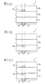
(1)図3の断面図に示すように、非発光部22に対応する、有機層20と透明電極10との間、及び/又は有機層20と背面電極30との間に絶縁部40を設ける。
すなわち、図3(a)に示すように、有機層20の背面電極30側に接するように絶縁部40を設けて非発光部22を形成したり、図3(b)に示すように、有機層20の透明電極10側に接するように絶縁部40を設けて非発光部22を形成したりすればよい。また、図3(c)に示すように絶縁部40を有機層20の両側に設けてもよい。
(1) As shown in the cross-sectional view of FIG. 3, the insulating
That is, as shown in FIG. 3A, the insulating
これによって、電圧印加時に、有機層の絶縁部40と対応する部分に電荷(正孔及び/又は電子)が注入されなくなるため、非発光部22の有機層20から光が発せられない。
絶縁部40は、公知の有機EL素子に用いることができる絶縁材料を、非発光部22における有機層20表面全面に接するように、蒸着法やCVD法等の公知の薄膜形成法を用いて設ければよい。
As a result, when voltage is applied, charges (holes and / or electrons) are not injected into the portion corresponding to the insulating
The insulating
なお、有機層20が積層構造を採用する場合には、有機層20を構成する層中の少なくとも一箇所に絶縁部40を設けてもよい。
絶縁部40を形成する材料としては、透明電極10の材料の体積抵抗率の約10倍以上の体積抵抗率を有するものが採用でき、このような材料としては、例えば、透明性ポリマー、酸化物、ガラスなどを挙げることができる。
In addition, when the
As a material for forming the insulating
より具体的に言えば、好ましい透明性ポリマーとしては、ポリイミド、フッ素化ポリイミド、フッ素系樹脂、ポリアクリレート、ポリキノリン、ポリオキサジアゾール、環状構造を有するポリオレフィン、ポリアリレート、ポリカーボネート、ポリサルフォン、ラダー型ポリシロキサン等が挙げられる。 More specifically, preferred transparent polymers include polyimide, fluorinated polyimide, fluororesin, polyacrylate, polyquinoline, polyoxadiazole, polyolefin having a cyclic structure, polyarylate, polycarbonate, polysulfone, ladder type poly Examples thereof include siloxane.
また、好ましい酸化物としては、SiO2、Al2O3、Ta2O3、Si3N4、フッ素添加SiO2、MgO、YbO3などは、エッチング加工が可能な材料の好適例として挙げることができる。このような材料は、エッチング加工が容易なため、絶縁部40の形状を任意の(好適な)形状にすることができる。
Further, as preferable oxides, SiO 2 , Al 2 O 3 , Ta 2 O 3 , Si 3 N 4 , fluorine-added SiO 2 , MgO, YbO 3, and the like are given as preferable examples of materials that can be etched. Can do. Since such a material is easy to be etched, the shape of the insulating
さらに、上記した材料に加えて、感光性を有するフォトレジスト及びその硬化物も好適に採用できる。フォトレジスト法によって、前記同様に絶縁部40の形状を任意の形状に加工できるからである。
Furthermore, in addition to the materials described above, a photosensitive photoresist and its cured product can also be suitably employed. This is because the shape of the insulating
なお、有機層20等は、水や酸素等により劣化しやすいため、絶縁部40には含水量が0.1重量%以下、及びガス透過係数(JISK7126)が1×10⁻¹³cc・cm/(cm2・s・cmHg)以下の材料を採用することが好ましい。このような材料としては、例えば無機酸化物、無機窒化物または両者の組成物が挙げられる。
Since the
また、絶縁部40は、有機層20から発せられる波長の光を透過する機能(透過機能)や、上記光を散乱する機能(散乱機能)、反射する機能(反射機能)等を備えていてもよい。
The insulating
絶縁部40は、有機層20の光取出側とは反対側に設けられる場合で、特に、背面電極30が反射機能を備えている場合には、有機層20から発せられる波長の光を反射する機能(反射機能)を備えているとよい。これにより、有機層20から発せられた光のうちで光取出側とは反対側に出射された光の進行方向を光取出側へ変換することができる。また、非発光部22は、発光はしないが、光はある程度出射するようになるため、いわゆる黒点(ダークスポット)として判断される(肉眼で確認される)可能性を極めて低くすることができる。
The insulating
背面電極30が、コントラスト向上等の目的で、有機層20から発せられた光を吸収する機能(吸収機能)を備えている場合には、絶縁部40にも吸収機能を持たせるとよい。絶縁部40に吸収機能を持たせるには、前記したような材料の中から、絶縁部40形成時に上記光を吸収するものを選択して絶縁部40を形成すればよい。また、絶縁部40の周囲のみをこのような材料で形成してもよい。
In the case where the
また、絶縁部40は透過機能を備えていてもよい。これにより、有機層20から光取出側とは反対側に発せられた光を背面電極30へ到達させることができる。つまり、背面電極30は、例えば反射機能等の機能を有している場合、非発光部22においても発光部21と同様にその機能を発揮することが可能となる。
The insulating
当然、絶縁部40に前記した以外の公知の機能を持たせることも可能である。
透過機能を非発光部22に持たせるには、上記したような材料の中で、絶縁部40とされた際に上記光に対する透過性を備えた材料を用いて絶縁部40を作成すればよい。また、散乱機能は、絶縁部40内に屈折率の異なる材料で形成されたビーズ等を分散させたりするなど、公知の方法によって実現することができる。反射機能は、上記したような材料の中から反射機能を有する材料を選択して絶縁部40を形成することで形成できる。また、絶縁部40とは別個に、絶縁部40に隣接して反射部材を設けてもよい。
Of course, it is also possible to give the insulating part 40 a known function other than those described above.
In order to provide the
なお、散乱機能や反射機能は、絶縁部40の表面のみに設けるなど、絶縁部40の一部にのみ設けてもよい。
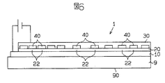
(2)非発光部22において、透明電極10、有機層20及び背面電極30の少なくとも一つを設けない。
Note that the scattering function and the reflection function may be provided only on a part of the insulating
(2) In the
例えば図4(a)に示すように、非発光部22における有機層20を設けないようにしたり、図4(b)に示すように、非発光部22における背面電極30を設けないようにしたり、図4(c)に示すように、非発光部22における透明電極10を設けないようにしたりしても非発光部22を形成できる。当然、これらの複数の層、さらにはすべての層を設けなくても非発光部22を構成できる。
For example, as shown in FIG. 4A, the
以上のような構成を採用すれば、非発光部22と対応する部分の有機層20に電流が流れないため、非発光部22から光が発しない。また、この構成を採用すれば、非発光部22において設けない層を有する分、有機EL素子1形成に必要な材料の量を少なくすることも可能になる。
If the configuration as described above is employed, no current flows through the portion of the
なお、このような構成を作成するには、例えば次のような製法を採用すればよい。
・マスク等を用いた、微細領域に薄膜を形成する方法を用いて発光部21にのみ透明電極10等を設ける。
In order to create such a configuration, for example, the following manufacturing method may be employed.
The
・印刷法等の微細領域に薄膜を形成できる方法を用いて透明電極10等を設ける。
・一旦透明電極10等を設けた後に非発光部22に対応する部分の透明電極10等を機械削剥やドライエッチング、ウェットエッチングなどの公知の微細加工法(除去法)を用いて除去する。
The
-After providing the
また、非発光部22において透明電極10等を設けない箇所には、有機EL素子1を保護するための保護部材を配置するとよい。この領域に空気等の有機EL素子1を劣化させる物質が存在することを防止したり、有機EL素子1を構成する各層の平滑性を保ったりするためである。例えば、透明電極10が設けられていない領域上に有機層20、背面電極30を設けると、有機層20及び背面電極30において、それぞれ段差ができてしまう可能性があるからである。また、有機層20が設けられていない領域上に背面電極30を設けると、透明電極10と背面電極30とが短絡してしまう可能性があるからである。
Further, a protective member for protecting the
(3)非発光部22における有機層20の膜厚を、発光部21におけるそれよりも厚くする。
有機層20は体積抵抗率が高いために、前記した構成を採用すれば、非発光部22を通る電流経路の抵抗率が高くなり、発光部21よりも電流が流れにくくなり、実質的に発光しなくなる。
(3) The thickness of the
Since the
(4)有機層20を変質させて、電圧が印加されても発光させないようにする。
有機層20を透明電極10上に略均一に形成した後、非発光部22に位置する有機層20に対して紫外線を照射したりレーザを照射したりするなどして、有機層20を変質させることで、電圧が印加されても発光させないようにする。このように処理された領域を非発光部22とすればよい。
(4) The
After the
次に、有機層20の一般的構成や製法等について説明する。
〈有機層20〉
有機層20は、透明電極10と背面電極30との間に設けられるとともに、両電極に電圧が印加されることで発光する有機発光材料を含有する層であり、公知の有機EL素子における公知の層構成及び公知の材料を使用すればよく、公知の製造方法によって製造できる。
Next, the general structure and manufacturing method of the
<
The
有機層20は、少なくとも以下の機能を実現できればよく、積層構造とし、各層にそれぞれいずれかの機能を担わせてもよく、単層により下記機能を実現してもよい。
・電子注入機能
電極(陰極)から電子を注入される機能。電子注入性。
The
-Electron injection function Function to inject electrons from the electrode (cathode). Electron injection.
・正孔注入機能
電極(陽極)から正孔(ホール)を注入される機能。正孔注入性。
・キャリア輸送機能
電子及び正孔の少なくとも一方を輸送する機能。キャリア輸送性。
-Hole injection function Function to inject holes from the electrode (anode). Hole injection property.
-Carrier transport function A function to transport at least one of electrons and holes. Carrier transportability.
電子を輸送する機能は電子輸送機能(電子輸送性)と言い、正孔を輸送する機能は正孔輸送機能(正孔輸送性)と言う。
・発光機能
注入・輸送された電子及び正孔を再結合させて励起子を発生させ(励起状態となり)、基底状態に戻る際に光を発する機能。
The function of transporting electrons is called an electron transport function (electron transportability), and the function of transporting holes is called a hole transport function (hole transportability).
-Light emitting function A function that emits light when returning to the ground state by recombining injected and transported electrons and holes to generate excitons (in an excited state).
透明電極10を陽極とする場合、有機層20は、例えば、透明電極10側から正孔注入輸送層、発光層、電子注入輸送層の順に層を設けて構成してもよい。
正孔注入輸送層は、陽極から発光層へ正孔を輸送する層である。正孔注入輸送層形成用の材料としては、例えば、銅フタロシアニン、テトラ(t−ブチル)銅フタロシアニン等の金属フタロシアニン類及び無金属フタロシアニン類、キナクリドン化合物、1、1−ビス(4−ジ−p−トリルアミノフェニル)シクロヘキサン、N、N’−ジフェニル−N、N’−ビス(3−メチルフェニル)−1、1’−ビフェニル−4、4’−ジアミン、N、N’−ジ(1−ナフチル)−N、N’−ジフェニル−1、1’−ビフェニル−4、4’−ジアミン等の芳香族アミンなどの低分子材料や、ポリチオフェン、ポリアニリン等の高分子材料、ポリチオフェンオリゴマー材料、その他既存の正孔輸送材料の中から選ぶことができる。
When the
The hole injecting and transporting layer is a layer that transports holes from the anode to the light emitting layer. Examples of the material for forming the hole injecting and transporting layer include metal phthalocyanines and metal-free phthalocyanines such as copper phthalocyanine and tetra (t-butyl) copper phthalocyanine, quinacridone compounds, and 1,1-bis (4-di-p -Tolylaminophenyl) cyclohexane, N, N′-diphenyl-N, N′-bis (3-methylphenyl) -1,1′-biphenyl-4,4′-diamine, N, N′-di (1- Naphthyl) -N, N′-diphenyl-1, 1′-biphenyl-4, 4′-diamine and other low molecular weight materials such as aromatic amines, polythiophene, polyaniline and other polymer materials, polythiophene oligomer materials, and other existing materials Of hole transport materials.
発光層は、陽極側から輸送された正孔と陰極側から輸送された電子とを再結合させて励起状態となり、励起状態から基底状態へ戻る際に光を発する層である。発光層の材料としては、蛍光材料や燐光材料を採用することができる。また、ホスト材中にドーパント(蛍光材料や燐光材料)を含有させてもよい。 The light-emitting layer is a layer that emits light when the holes transported from the anode side and the electrons transported from the cathode side are recombined to be in an excited state and return from the excited state to the ground state. As the material of the light emitting layer, a fluorescent material or a phosphorescent material can be employed. Further, a dopant (fluorescent material or phosphorescent material) may be contained in the host material.
発光層形成用の材料としては、例えば、9、10−ジアリールアントラセン誘導体、ピレン誘導体、コロネン誘導体、ペリレン誘導体、ルブレン誘導体、1、1、4、4−テトラフェニルブタジエン、トリス(8−キノリノラート)アルミニウム錯体、トリス(4−メチル−8−キノリノラート)アルミニウム錯体、ビス(8−キノリノラート)亜鉛錯体、トリス(4−メチル−5−トリフルオロメチル−8−キノリノラート)アルミニウム錯体、トリス(4−メチル−5−シアノ−8−キノリノラート)アルミニウム錯体、ビス(2−メチル−5−トリフルオロメチル−8−キノリノラート)[4−(4−シアノフェニル)フェノラート]アルミニウム錯体、ビス(2−メチル−5−シアノ−8−キノリノラート)[4−(4−シアノフェニル)フェノラート]アルミニウム錯体、トリス(8−キノリノラート)スカンジウム錯体、ビス〔8−(パラ−トシル)アミノキノリン〕亜鉛錯体及びカドミウム錯体、1、2、3、4−テトラフェニルシクロペンタジエン、ペンタフェニルシクロペンタジエン、ポリ−2、5−ジヘプチルオキシ−パラ−フェニレンビニレン、クマリン系蛍光体、ペリレン系蛍光体、ピラン系蛍光体、アンスロン系蛍光体、ポルフィリン系蛍光体、キナクリドン系蛍光体、N、N’−ジアルキル置換キナクリドン系蛍光体、ナフタルイミド系蛍光体、N、N’−ジアリール置換ピロロピロ−ル系蛍光体等の低分子材料や、ポリフルオレン、ポリパラフェニレンビニレン、ポリチオフェン等の高分子材料、その他既存の発光材料を用いることができる。ホスト/ゲスト型の構成を採用する場合には、これらの材料の中から適宜ホスト及びゲスト(ド−パント)を選択すればよい。 Examples of the material for forming the light emitting layer include 9,10-diarylanthracene derivatives, pyrene derivatives, coronene derivatives, perylene derivatives, rubrene derivatives, 1,1,4,4-tetraphenylbutadiene, tris (8-quinolinolato) aluminum. Complex, tris (4-methyl-8-quinolinolato) aluminum complex, bis (8-quinolinolato) zinc complex, tris (4-methyl-5-trifluoromethyl-8-quinolinolato) aluminum complex, tris (4-methyl-5) -Cyano-8-quinolinolato) aluminum complex, bis (2-methyl-5-trifluoromethyl-8-quinolinolato) [4- (4-cyanophenyl) phenolate] aluminum complex, bis (2-methyl-5-cyano- 8-quinolinolato) [4- (4-cyanophe L) phenolate] aluminum complex, tris (8-quinolinolato) scandium complex, bis [8- (para-tosyl) aminoquinoline] zinc complex and cadmium complex, 1,2,3,4-tetraphenylcyclopentadiene, pentaphenylcyclo Pentadiene, poly-2,5-diheptyloxy-para-phenylene vinylene, coumarin phosphor, perylene phosphor, pyran phosphor, anthrone phosphor, porphyrin phosphor, quinacridone phosphor, N, N Low-molecular materials such as' -dialkyl-substituted quinacridone phosphors, naphthalimide-based phosphors, N, N'-diaryl-substituted pyrrolopyrrole phosphors, polymer materials such as polyfluorene, polyparaphenylene vinylene, polythiophene, Other existing light emitting materials can be used. In the case of adopting a host / guest type configuration, a host and a guest (dopant) may be appropriately selected from these materials.
電子注入輸送層は、陰極(本例では背面電極30)から発光層へ電子を輸送する層である。電子注入輸送層形成用の材料としては、例えば、2−(4−ビフィニルイル)−5−(4−t−ブチルフェニル)−1、3、4−オキサジアゾール、2、5−ビス(1−ナフチル)−1、3、4−オキサジアゾール及びオキサジアゾール誘導体やビス(10−ヒドロキシベンゾ[h]キノリノラート)ベリリウム錯体、トリアゾ−ル化合物等が挙げられる。
The electron injection transport layer is a layer that transports electrons from the cathode (back
なお、有機層20には、バッファ層や正孔ブロック層、電子注入層、正孔注入層等の公知の有機エレクトロルミネッセンス層に採用されうる層を設けることも当然に可能である。これらの層も、公知の材料を用いて公知の製法によって設けることができる。例えば電子注入輸送層を、電子注入機能を担う電子注入層と電子輸送機能を担う電子輸送層とに機能分離して積層してもよい。これらの各層を構成する材料は、各層の機能に応じて、公知の材料から適宜選択すればよく、上記した電子注入輸送層形成用の材料の中から選択することもできる。
It should be noted that the
次に透明電極10及び背面電極30についてあわせて説明する。
〈電極〉
透明電極10及び背面電極30は、一方が陽極として機能し、他方が陰極として機能する。本実施形態においては、いずれの電極が陽極であっても(陰極であっても)構わない。まず、陽極について説明する。
Next, the
<electrode>
One of the
(陽極)
陽極は、有機層20に正孔(ホール)を注入する電極である。
陽極形成用の材料は、上記した性質を電極に付与する材料であればよく、一般には金属、合金、電気伝導性の化合物及びこれらの混合物等、公知の材料が選択される。
(anode)
The anode is an electrode that injects holes into the
The material for forming the anode may be any material that imparts the above-described properties to the electrode, and generally known materials such as metals, alloys, electrically conductive compounds, and mixtures thereof are selected.
陽極形成用の材料としては、例えば以下のものを挙げることができる。
ITO(インジウム−スズ−オキサイド)、
IZO(インジウム−亜鉛−オキサイド)、
酸化スズ、酸化亜鉛、亜鉛アルミニウム酸化物、窒化チタン等の金属酸化物や金属窒化物;
金、白金、銀、銅、アルミニウム、ニッケル、コバルト、鉛、クロム、モリブデン、タングステン、タンタル、ニオブ等の金属;
これらの金属の合金やヨウ化銅の合金等、
ポリアニリン、ポリチオフェン、ポリピロール、ポリフェニレンビニレン、ポリ(3−メチルチオフェン)、ポリフェニレンスルフィド等の導電性高分子、など。
Examples of the material for forming the anode include the following.
ITO (indium-tin-oxide),
IZO (indium-zinc-oxide),
Metal oxides and metal nitrides such as tin oxide, zinc oxide, zinc aluminum oxide, titanium nitride;
Metals such as gold, platinum, silver, copper, aluminum, nickel, cobalt, lead, chromium, molybdenum, tungsten, tantalum, niobium;
These metal alloys and copper iodide alloys,
Conductive polymers such as polyaniline, polythiophene, polypyrrole, polyphenylene vinylene, poly (3-methylthiophene), polyphenylene sulfide, and the like.
透明電極10を陽極とする場合には、一般に、取り出す光に対する透過率が10%よりも大きくなるように設定される。可視光領域の光を取り出す場合には、可視光領域で透過率の高いITOが好適に用いられる。
When the
背面電極30を陽極とする場合には、好ましくは反射性電極として構成される。この場合、以上のような材料の内、外部へ取り出す光を反射する機能を備えた材料が適宜選択され、一般には金属や合金、金属化合物が選択される。
When the
また、コントラスト等を防止したり、外光の反射を防止したりするために、背面電極30に光の吸収機能を持たせてもよい。背面電極30に吸収機能を持たせるには、前記したような材料の中から、電極を形成した際に吸収機能を発揮する材料を適宜選択すればよい。
Further, the
陽極は、上記したような材料一種のみで形成してもよく、複数を混合して形成してもよい。また、同一組成又は異種組成の複数層からなる複層構造であってもよい。
陽極の膜厚は、使用する材料にもよるが、一般に5nm〜1μm程度、好ましくは10nm〜1μm程度、さらに好ましくは10nm〜500nm程度、特に好ましくは10nm〜300nm程度、望ましくは10nm〜200nmの範囲で選択される。
The anode may be formed of only one kind of material as described above, or may be formed by mixing a plurality of materials. Moreover, the multilayer structure which consists of several layers of the same composition or a different composition may be sufficient.
Although the film thickness of the anode depends on the material used, it is generally in the range of about 5 nm to 1 μm, preferably about 10 nm to 1 μm, more preferably about 10 nm to 500 nm, particularly preferably about 10 nm to 300 nm, desirably 10 nm to 200 nm. Selected.
陽極は、上記したような材料を用いて、スパッタリング法やイオンプレーティング法、真空蒸着法、スピンコート法、電子ビーム蒸着法などの公知の薄膜形成法によって形成される。 The anode is formed by a known thin film forming method such as a sputtering method, an ion plating method, a vacuum evaporation method, a spin coating method, or an electron beam evaporation method using the above-described materials.
陽極のシート電気抵抗は、好ましくは、数百Ω/□以下、より好ましくは、5〜50Ω/□程度に設定される。
また、陽極の表面を、UVオゾン洗浄やプラズマ洗浄してもよい。
The sheet electrical resistance of the anode is preferably set to several hundred Ω / □ or less, more preferably about 5 to 50 Ω / □.
Further, the surface of the anode may be subjected to UV ozone cleaning or plasma cleaning.
有機EL素子の短絡や欠陥の発生を抑制するためには、粒径を微小化する方法や成膜後に研磨する方法により、表面の粗さを二乗平均値として20nm以下に制御するとよい。
(陰極)
陰極は、有機層20(上記層構成では電子注入輸送層)に電子を注入する電極である。
In order to suppress the occurrence of short circuits and defects in the organic EL element, the surface roughness may be controlled to 20 nm or less as a mean square value by a method of reducing the particle size or a method of polishing after film formation.
(cathode)
The cathode is an electrode that injects electrons into the organic layer 20 (in the above-described layer configuration, an electron injection transport layer).
陰極形成用の材料としては、電子注入効率を高くするために仕事関数が例えば4.5eV未満、一般には4.0eV以下、典型的には3.7eV以下の金属や合金、電気伝導性化合物及びこれらの混合物が採用される。 As a material for forming the cathode, a metal, an alloy, an electrically conductive compound having a work function of, for example, less than 4.5 eV, generally 4.0 eV or less, typically 3.7 eV or less in order to increase electron injection efficiency, and A mixture of these is employed.
以上のような電極物質としては、例えば、リチウム、ナトリウム、マグネシウム、金、銀、銅、アルミニウム、インジウム、カルシウム、スズ、ルテニウム、チタニウム、マンガン、クロム、イットリウム、アルミニウム−カルシウム合金、アルミニウム−リチウム合金、アルミニウム−マグネシウム合金、マグネシウム−銀合金、マグネシウム−インジウム合金、リチウム−インジウム合金、ナトリウム−カリウム合金、マグネシウム/銅混合物、アルミニウム/酸化アルミニウム混合物などが挙げられる。また、陽極に用いられる材料として採用できる材料も使用できる。 Examples of the electrode material as described above include lithium, sodium, magnesium, gold, silver, copper, aluminum, indium, calcium, tin, ruthenium, titanium, manganese, chromium, yttrium, aluminum-calcium alloy, and aluminum-lithium alloy. , Aluminum-magnesium alloys, magnesium-silver alloys, magnesium-indium alloys, lithium-indium alloys, sodium-potassium alloys, magnesium / copper mixtures, aluminum / aluminum oxide mixtures, and the like. Moreover, the material employable as a material used for an anode can also be used.
背面電極30が陰極とされる場合には、以上のような材料の内、外部へ取り出す光を反射する機能を備えた材料が好ましく選択され、一般には金属や合金、金属化合物が選択される。
When the
透明電極10が陰極とされる場合には、一般に、取り出す光に対する透過率が10%よりも大きくなるように設定され、例えば、超薄膜のマグネシウム−銀合金に透明な導電性酸化物を積層化して形成された電極などが採用される。また、この陰極において、導電性酸化物をスパッタリングする際に発光層などがプラズマにより損傷するのを防ぐため、銅フタロシアニンなどを添加したバッファ層を陰極と有機層20との間に設けるとよい。
When the
陰極は、以上のような材料単独で形成してもよいし、複数の材料によって形成してもよい。例えば、マグネシウムに銀や銅を5%〜10%添加させれば、陰極の酸化を防止でき、また陰極の有機層20との接着性も高くなる。
The cathode may be formed of the above materials alone or a plurality of materials. For example, if 5% to 10% of silver or copper is added to magnesium, the oxidation of the cathode can be prevented, and the adhesion of the cathode to the
また、陰極は、同一組成又は異種組成の複数層からなる複層構造であってもよい。例えば以下のような構造にしてもよい。
・陰極の酸化を防ぐため、陰極の有機層20と接しない部分に、耐食性のある金属からなる保護層を設ける。この保護層形成用の材料としては例えば銀やアルミニウムなどが好ましく用いられる。
The cathode may have a multilayer structure composed of a plurality of layers having the same composition or different compositions. For example, the following structure may be used.
In order to prevent oxidation of the cathode, a protective layer made of a corrosion-resistant metal is provided on the portion of the cathode that does not contact the
・陰極の仕事関数を小さくするために、陰極と有機層20との界面部分に仕事関数の小さな酸化物やフッ化物、金属化合物等を挿入する。
例えば、陰極の材料をアルミニウムとし、界面部分にフッ化リチウムや酸化リチウムを挿入したものも用いられる。
In order to reduce the work function of the cathode, an oxide, fluoride, metal compound or the like having a small work function is inserted into the interface portion between the cathode and the
For example, a material in which the cathode material is aluminum and lithium fluoride or lithium oxide is inserted in the interface portion is also used.
陰極は、真空蒸着法、スパッタリング法、イオン化蒸着法、イオンプレーティング法、電子ビーム蒸着法などの公知の薄膜成膜法によって形成できる。
陰極のシート電気抵抗は、数百Ω/□以下に設定することが好ましい。
The cathode can be formed by a known thin film deposition method such as a vacuum deposition method, a sputtering method, an ionization deposition method, an ion plating method, or an electron beam deposition method.
The sheet electrical resistance of the cathode is preferably set to several hundred Ω / □ or less.
次いで、有機EL素子1に好ましく採用される層や部材について説明する。
(絶縁層)
透明電極10と背面電極30とが短絡しないようにするために、有機層20の外周に絶縁層を設けるとよい。このように絶縁層を設けることで、電気的に隣接する発光領域の透明電極10やその背面電極30が有機層20と接触することも防止できる。
Next, layers and members that are preferably employed in the
(Insulating layer)
In order to prevent the
絶縁層形成用の材料としては、公知の有機EL素子に採用される絶縁部形成用の材料を適宜採用することができ、例えば、上記した絶縁部40形成用の材料を採用することもできる。形成方法も公知の形成方法を採用でき、例えばスパッタ法、電子線蒸着法、CVD法等を採用することができる。
As a material for forming the insulating layer, a material for forming an insulating portion employed in a known organic EL element can be appropriately employed. For example, the material for forming the insulating
(補助電極)
補助電極を設けることも当然に可能である。補助電極は、陽極及び/又は陰極に電気的に接続するように設けられ、接続する電極よりも体積抵抗率の低い材料で構成される。このような材料により補助電極を形成すれば、補助電極が設けられた電極全体の体積抵抗率を下げることが可能となり、有機層20を構成する各点に流れる電流の大きさの最大差を、補助電極を設けない場合と比べて小さくできる。
(Auxiliary electrode)
It is naturally possible to provide an auxiliary electrode. The auxiliary electrode is provided so as to be electrically connected to the anode and / or the cathode, and is made of a material having a lower volume resistivity than the electrode to be connected. If the auxiliary electrode is formed of such a material, it becomes possible to reduce the volume resistivity of the entire electrode provided with the auxiliary electrode, and the maximum difference in the magnitude of the current flowing to each point constituting the
補助電極形成用の材料としては、例えば、タングステン(W)、アルミニウム(Al)、銅(Cu)、銀(Ag)、モリブデン(Mo)、タンタル(Ta)、金(Au)、クロム(Cr)、チタン(Ti)、ネオジウム(Nd)、及びこれらの合金を挙げることができる。 Examples of the material for forming the auxiliary electrode include tungsten (W), aluminum (Al), copper (Cu), silver (Ag), molybdenum (Mo), tantalum (Ta), gold (Au), and chromium (Cr). , Titanium (Ti), neodymium (Nd), and alloys thereof.
また、これらの合金の具体例としては、Mo−W、Ta−W、Ta−Mo、Al−Ta、Al−Ti、Al−Nd、Al−Zr等の合金を挙げることができる。さらに、補助配線層の構成材料としては、金属とケイ素の化合物である、TiSi2、ZrSi2、HfSi2、VSi2、NbSi2、TaSi2、CrSi2、WSi2、CoSi2、NiSi2、PtSi、Pd2Siなども好ましい。また、これらの金属やケイ素化合物をそれぞれ積層した構成であってもよい。
Specific examples of these alloys include alloys such as Mo—W, Ta—W, Ta—Mo, Al—Ta, Al—Ti, Al—Nd, and Al—Zr. Further, as the material of the auxiliary wiring layer, which is a compound of metal and silicon, TiSi 2, ZrSi 2, HfSi 2,
なお、補助電極は、上記したような材料による単層の膜であってもよいが、膜の安定性を高める上で二種以上の多層膜とすることも好ましい。このような多層膜としては、上記金属またはそれらの合金を用いて形成することができる。例えば、三層の場合、Ta層とCu層とTa層、及びTa層とAl層とTa層、二層の場合、Al層とTa層、Cr層とAu層、Cr層とAl層、及びAl層とMo層の組合せを挙げることができる。 The auxiliary electrode may be a single-layer film made of the above materials, but it is also preferable to use two or more types of multilayer films in order to improve the stability of the film. Such a multilayer film can be formed using the above metals or their alloys. For example, in the case of three layers, Ta layer and Cu layer and Ta layer, and Ta layer and Al layer and Ta layer, in the case of two layers, Al layer and Ta layer, Cr layer and Au layer, Cr layer and Al layer, and A combination of an Al layer and a Mo layer can be given.
ここで、膜の安定性とは、低体積抵抗率を維持しうるとともに、エッチングの際、その処理に用いる液等により腐食されにくい性質をいう。たとえば、補助電極をCuやAgで構成した場合には、補助電極の体積抵抗率自体は低いものの、腐食しやすい場合がある。それに対して、CuやAgからなる金属膜の上部及び下部、あるいはいずれか一方に、耐食性に優れた金属、例えばTa、Cr、Mo等の膜を積層することにより、補助電極の安定性を高めることができる。 Here, the stability of the film refers to a property that can maintain a low volume resistivity and is not easily corroded by a liquid or the like used for the treatment during etching. For example, when the auxiliary electrode is made of Cu or Ag, the auxiliary electrode may have a low volume resistivity but may be easily corroded. On the other hand, the stability of the auxiliary electrode is enhanced by laminating a metal with excellent corrosion resistance, such as Ta, Cr, Mo, etc., on the upper and / or lower part of the metal film made of Cu or Ag. be able to.
補助電極の膜厚は、一般には100nm〜数10μmの範囲内の値とすることが好ましく、特に好ましくは200nm〜5μmの範囲内の値とすることである。
この理由は、かかる膜厚が100nm未満となると、抵抗値が大きくなり、補助電極として好ましくなく、一方、かかる膜厚が数10μmを超えると平坦化しにくくなり、有機EL素子1の欠陥が生じるおそれがあるためである。
In general, the thickness of the auxiliary electrode is preferably set to a value within the range of 100 nm to several tens of μm, and more preferably set to a value within the range of 200 nm to 5 μm.
The reason for this is that when the film thickness is less than 100 nm, the resistance value increases, which is not preferable as the auxiliary electrode. On the other hand, when the film thickness exceeds several tens of μm, it becomes difficult to flatten and the
補助電極の幅は、例えば、2μm〜1、000μmの範囲内の値とすることが好ましく、5μm〜300μmの範囲内の値とすることがより好ましい。
この理由は、かかる幅が2μm未満となると、補助電極の抵抗が大きくなる場合があるためであり、一方、かかる幅が1000μmを超えると、外部への光の取り出しを妨害する場合があるためである。
For example, the width of the auxiliary electrode is preferably a value within a range of 2 μm to 1,000 μm, and more preferably a value within a range of 5 μm to 300 μm.
This is because when the width is less than 2 μm, the resistance of the auxiliary electrode may increase. On the other hand, when the width exceeds 1000 μm, the extraction of light to the outside may be hindered. is there.
(保護層:パッシベーション膜、封止缶)
有機層20等を外気から保護するために、有機EL素子1をパッシベーション膜や封止缶によって保護してもよい。
(Protective layer: passivation film, sealed can)
In order to protect the
パッシベーション膜は、有機EL素子1が酸素や水分と接触するのを防止するために透明基板9と反対側に設けられる保護層(封止層)である。パッシベーション膜に使用する材料としては、例えば、有機高分子材料、無機材料、さらには光硬化性樹脂などを挙げることができ、保護層に使用する材料は、単独で使用してもよく、あるいは複数併用してもよい。保護層は、一層構造であってもよく、また多層構造であってもよい。パッシベーション膜の膜厚は、外部からの水分やガスを遮断できる厚さであればよい。
The passivation film is a protective layer (sealing layer) provided on the side opposite to the
有機高分子材料の例としては、クロロトリフルオロエチレン重合体、ジクロロジフルオロエチレン重合体、クロロトリフルオロエチレン重合体とジクロロジフルオロエチレン重合体との共重合体等のフッ素系樹脂、ポリメチルメタクリレート、ポリアクリレート等のアクリル系樹脂、エポキシ樹脂、シリコン樹脂、エポキシシリコーン樹脂、ポリスチレン樹脂、ポリエステル樹脂、ポリカーボネート樹脂、ポリアミド樹脂、ポリイミド樹脂、ポリアミドイミド樹脂、ポリパラキシレン樹脂、ポリエチレン樹脂、ポリフェニレンオキサイド樹脂などを挙げることができる。 Examples of organic polymer materials include fluorinated resins such as chlorotrifluoroethylene polymer, dichlorodifluoroethylene polymer, a copolymer of chlorotrifluoroethylene polymer and dichlorodifluoroethylene polymer, polymethyl methacrylate, poly Acrylic resins such as acrylate, epoxy resins, silicone resins, epoxy silicone resins, polystyrene resins, polyester resins, polycarbonate resins, polyamide resins, polyimide resins, polyamideimide resins, polyparaxylene resins, polyethylene resins, polyphenylene oxide resins, etc. be able to.
無機材料としては、ポリシラザン、ダイヤモンド薄膜、アモルファスシリカ、電気絶縁性ガラス、金属酸化物、金属窒化物、金属炭素化物、金属硫化物などを挙げることができる。 Examples of the inorganic material include polysilazane, diamond thin film, amorphous silica, electrically insulating glass, metal oxide, metal nitride, metal carbonide, metal sulfide and the like.
封止缶は、外部からの水分や酸素を遮断するための、封止板、封止容器等の封止部材により構成される部材である。封止缶は、背面側の電極側(透明基板9とは反対側)のみに設置しても、有機EL素子1全体を覆ってもよい。封止部材は、有機EL素子1を封止でき外部の空気を遮断することができればよく、封止部材の形状、大きさ、厚さ等は特に限定されない。封止部材に用いる材料としては、ガラス、ステンレススチール、金属(アルミニウム等)、プラスチック(ポリクロロトリフルオロエチレン、ポリエステル、ポリカーボネート等)、セラミック等が使用できる。
The sealing can is a member constituted by a sealing member such as a sealing plate or a sealing container for blocking moisture and oxygen from the outside. The sealing can may be installed only on the electrode side on the back side (the side opposite to the transparent substrate 9) or may cover the entire
封止部材を有機EL素子1に設置する際には、適宜封止剤(接着剤)を用いてもよい。有機EL素子1全体を封止部材で覆う場合は、封止剤を用いずに封止部材同士を熱融着してもよい。封止剤としては紫外線硬化樹脂、熱硬化樹脂、二液型硬化樹脂等が使用可能である。
When installing the sealing member on the
なお、パッシベーション膜や封止缶と有機EL素子1との間の空間に水分吸収剤を挿入してもよい。水分吸収剤は特に限定されず、具体例としては酸化バリウム、酸化ナトリウム、酸化カリウム、酸化カルシウム、硫酸ナトリウム、硫酸カルシウム、硫酸マグネシウム、五酸化リン、塩化カルシウム、塩化マグネシウム、塩化銅、フッ化セシウム、フッ化ニオブ、臭化カルシウム、臭化バナジウム、モレキュラーシーブ、ゼオライト、酸化マグネシウム等が挙げられる。
A moisture absorbent may be inserted into the space between the passivation film or the sealing can and the
また、パッシベーション膜や封止缶内に不活性なガスを封入してもよい。不活性なガスとは、有機EL素子1と反応しないガスのことをいい、例えばヘリウム、アルゴン等の希ガスや窒素ガスを採用することができる。
Further, an inert gas may be enclosed in the passivation film or the sealing can. The inert gas refers to a gas that does not react with the
次に基板について説明する。
〈基板〉
基板は、有機EL素子1を支える、主として板状の部材である。有機EL素子1は、構成する各層が非常に薄いため、一般に基板によって支えられた有機EL装置として作製される。
Next, the substrate will be described.
<substrate>
The substrate is a mainly plate-like member that supports the
基板は、有機EL素子1が積層される部材であるため、平面平滑性を有していることが好ましい。
また、基板は、有機層20よりも光取り出し側にある場合には取り出す光に対して透明とされる。この実施形態の有機EL素子1はボトムエミッション型の素子であるため、基板は、透明であり、また、透明基板9の有機EL素子1と接する平面とは反対側の平面が光取出面90とされる。
Since the substrate is a member on which the
Further, when the substrate is on the light extraction side with respect to the
基板としては、上記した機能を有していれば公知のものを用いることができる。一般には、ガラス基板やシリコン基板、石英基板などのセラミックス基板や、プラスチック基板が選択される。また、金属基板や支持体に金属箔を形成した基板なども用いられる。さらに、同種又は異種の基板を複数組み合わせた複合シートからなる基板を用いることもできる。 Any known substrate can be used as long as it has the above-described functions. In general, a ceramic substrate such as a glass substrate, a silicon substrate, or a quartz substrate, or a plastic substrate is selected. Moreover, the board | substrate etc. which formed metal foil in the metal substrate and the support body are used. Furthermore, a substrate made of a composite sheet in which a plurality of substrates of the same type or different types are combined can also be used.
なお、上記例では、透明基板9上に透明電極10、有機層20及び背面電極30を順次積層したボトムエミッション型の有機EL装置を示したが、有機EL装置として構成せず、透明基板9を有しない有機EL素子1として構成してもよいことは当然である。この場合には、はじめから基板を用いずに有機EL素子1を製造してもよく、又は、有機EL装置作製後に基板をエッチング等の公知の基板削剥技術により削除して有機EL素子1を製造してもよい。
In the above example, the bottom emission type organic EL device in which the
また、トップエミッション型装置として構成しても、両側から光を取り出す装置として構成してもよいことは前記したとおりである。
すなわち、ボトムエミッション型の有機EL素子1を製造するには、透明基板9上に、透明電極10、有機層20及び背面電極30を、前記したそれぞれの成膜方法を用いて成膜すればよい。トップエミッション型の有機EL素子を製造するには、基板上に、背面電極30、有機層20及び透明電極10を順次成膜すればよい。
Further, as described above, it may be configured as a top emission type device or a device that extracts light from both sides.
That is, in order to manufacture the bottom emission type
次に、上記有機EL素子1の作用及び効果について説明する。
〈作用及び効果〉
有機EL素子1における透明電極10及び背面電極30は、それぞれの端子部11、31で外部駆動回路と接続される。そして、外部駆動回路によって有機EL素子に電圧が印加されると、有機層に電圧が印加される。この際、発光部21は発光し、非発光部22は発光しない。
Next, the operation and effect of the
<Action and effect>
The
前記したように非発光部22は、体積抵抗率の高い電極(本例では透明電極10)の端子部11に近いほど、単位面積当たりに占める面積が広い。また、端子部11に近いほど、発光部21における電流密度は大きい。したがって、有機層20の非発光部22の1つの面積よりも十分に大きな単位面積当たりにおいて、有機層20を流れる電流量は、端子部11からの距離によってその大きさをほぼ同じにすることができる。
As described above, the
また、前記した説明中に記載した各作用や効果も当然得ることができる。
次に、本発明を、有機EL素子の輝度分布の所望状態として、素子の中央部分が両サイドに比較して輝度が高くなる状態の有機EL素子に具体化した実施形態について、図5及び図6を参照して説明する。なお、前記実施形態と同一又は相当する部分には同一符号を付して詳しい説明を省略する。図5は有機層20と非発光部22との関係を示す模式正面図であり、図6は有機EL装置の模式断面図である。なお、図6において断面を示すハッチングを省略している。
In addition, it is possible to obtain the operations and effects described in the above description.
Next, an embodiment in which the present invention is embodied as an organic EL element in which the central portion of the element has a higher luminance than both sides as a desired state of the luminance distribution of the organic EL element will be described with reference to FIGS. This will be described with reference to FIG. In addition, the same code | symbol is attached | subjected to the part which is the same as that of the said embodiment, or detailed description is abbreviate | omitted. FIG. 5 is a schematic front view showing the relationship between the
図6に示すように、有機EL装置は、透明基板9上に、透明電極10、有機層20及び背面電極30が順に形成されている。有機層20の背面電極30側の面には絶縁部40が複数箇所に設けられており、有機層20の絶縁部40と対応する部分が非発光部22を構成する。即ち、有機層20は絶縁部40の数と同数の非発光部22を有する。なお、有機EL素子1は、透明基板9と対向する面を除いた部分が、図示しない、パッシベーション膜により保護されている。
As shown in FIG. 6, in the organic EL device, a
透明電極10の端子部11は、前記実施形態と同様に透明電極10の一端側の隅部に設けられている。したがって、有機層20に非発光部22を設けない状態で、透明電極10及び背面電極30間に電圧が印加された場合は、端子部11に物理的に近い領域ほど輝度が高くなる。
The
この輝度分布が、非発光部22を設けることによって、有機EL素子1の中央部分の所定領域51が両サイドの領域52a,52bに比較して輝度が高くなる状態になるように調整されている。具体的には、複数の非発光部22が設けられ、非発光部22は、該非発光部22を設けない状態から有機層20の発光時の輝度を低下させたい割合が大きい領域ほど、単位面積当たりに占める面積が大きくなるように設けられている。
This luminance distribution is adjusted so that the
非発光部22を設ける前の発光時の状態では、端子部11に近い領域ほど輝度が高い。したがって、中央部分の所定領域51が両サイドの領域52a,52bに比較して輝度が高くなるようにするためには、端子部11に近い領域52aでは非発光部22の割合を中央部分の所定領域51より多くする。中央部分の所定領域51内でも、端子部11に近い側の方が遠い側の方より非発光部22の分布割合が多くなるように設けられる。また、端子部11から遠い側の領域52bでは、領域51に近い側では隣接する領域51の部分より非発光部22の分布割合が多くなるが、領域51から離れるほど少なくなるため、場合によっては領域51から離れた部分における非発光部22の分布割合が領域51における非発光部22の分布割合より少なくなることもある。
In the state at the time of light emission before providing the
この実施形態において、有機EL素子1を構成する有機層20、発光部21、非発光部22、透明電極10、背面電極30等の各部の構成は、前記実施形態の場合と同様に種々の構成が可能である。また、基板、絶縁層、補助電極、保護層(パッシベーション膜、封止缶)等も前記実施形態の場合と同様に種々の構成が可能である。
In this embodiment, the configuration of each part such as the
この実施形態においても、有機EL素子1における透明電極10及び背面電極30は、それぞれの端子部11、31を介して外部駆動回路と接続される。そして、外部駆動回路によって有機EL素子1に電圧が印加されると、有機層20に電圧が印加される。この際、発光部21は発光し、非発光部22は発光しない。そして、非発光部22が上記のような分布で設けられているため、素子の中央部分の所定領域51が両サイドの領域52a,52bに比較して輝度が高くなる状態に発光する。
Also in this embodiment, the
また、前記実施形態の構成に基づく作用や効果のうち、この実施形態においても同一の構成の部分に関してはそれらの作用効果も当然得ることができる。例えば、絶縁部40を反射率の高い材質で形成することにより、同じ輝度を得るのに必要な消費電力を低くできる。
Of the operations and effects based on the configuration of the above-described embodiment, those operations and effects can also be obtained for the same configuration in this embodiment. For example, the power consumption necessary to obtain the same luminance can be reduced by forming the insulating
次に、絶縁部40を設けることにより非発光部22を形成して、有機EL素子1の中央部分の所定領域が両サイドの領域に比較して輝度が高くなる状態の有機EL素子に具体化した別の実施形態について、図7及び図8を参照して説明する。なお、前記実施形態と同一又は相当する部分には同一符号を付して詳しい説明を省略する。
Next, the non-light-emitting
図7に示すように、この実施形態では絶縁部40が透明電極10(陽極)と有機層20との間に設けられ、透明基板9と透明電極10との間の前記絶縁部40と対応する位置にそれぞれ光反射層23が設けられている点が前記実施形態と異なり、その他の点は同じである。
As shown in FIG. 7, in this embodiment, an insulating
前記実施形態では絶縁部40が有機層20と背面電極30との間に設けられているため、有機層20を形成した後に絶縁部40を形成する必要がある。絶縁部40は予め設定された分布となるように形成する必要があり、有機層20上に一平面となるように形成するのではなく、パターン形成を必要とする。有機層20は、水分や高熱に弱いため、エッチングなどで不要な部分を除去して必要な箇所に絶縁部40を形成する方法では、有機層20を損傷しないようにするための製造条件が厳しくなる。
In the embodiment, since the insulating
しかし、この実施形態では、絶縁部40は透明電極10と有機層20との間に設けられているため、絶縁部40を形成した後、有機層20を形成することが可能となり、絶縁部40を形成する際の自由度が高くなる。例えば、絶縁部40はポジタイプのフォトレジストで形成され、所定の分布(パターン)の絶縁部40が形成される。そして、フォトレジストを露光する際に絶縁部40となる部分以外の部分を露光するためのマスクを特に設けなくても、光反射層23が形成された透明基板9がマスクの役割を果たす。
However, in this embodiment, since the insulating
具体的には、透明基板9上に有機EL素子1を形成する工程において、透明基板9の所定位置(絶縁部40が形成される位置と対応する位置)に光反射層23が形成された後、図8(a)に示すように、その上に透明電極10が形成される。光反射層23は、例えば銀で形成される。次に透明電極10の上にフォトレジスト層24が形成された後、図8(b)に示すように、透明基板9側から露光され、フォトレジスト層24の光反射層23と対応する部分以外の部分が可溶性となる。次に、可溶性となった部分を除去し、図8(c)に示すように、光反射層23と対応する部分に絶縁部40が形成される。以下、有機層20、背面電極30及び保護層(図示せず)が形成されて有機EL装置が形成される。なお、図7では、便宜上、有機層20を絶縁部40より厚く図示しているが、実際は絶縁部40の方が厚い。
Specifically, in the step of forming the
この実施形態においても前記実施形態と同様に、有機EL素子1に電圧が印加されると、素子の中央部分の所定領域51が両サイドの領域52a,52bに比較して輝度が高くなる状態に発光する。そして、この実施形態においては、輝度分布を決める絶縁部40がフォトレジストで形成され、その露光時に使用されるマスクの役割を光反射層23が形成された透明基板9が果たすため、絶縁部40が設計どおりの位置に精度良く形成される。また、輝度分布を設計どおりにするためには、絶縁部40と対応する位置、即ち非発光部22と対応する箇所からは光が出射しない方が設計が容易である。この実施形態では、絶縁部40と対応する位置に光反射層23が形成されているため、絶縁部40が光を一部透過させてもその光が透明基板9から出射されるのが光反射層23で阻止され、設計通りの輝度分布を得るのが容易になる。また、非発光部22では、透明基板9の光取出面90側から有機EL素子1の内部に向かう光が、光反射層23で反射される。よって、例えば、有機層や透明電極が光を吸収する機能を備えている場合には、これらの光を吸収する層を透過せずに光反射層23で反射されるため、前記実施形態よりも光損失が小さくなり、低消費電力化を図れる。
Also in this embodiment, when a voltage is applied to the
次に本発明を、有機EL素子の輝度分布の所望状態として、有機EL素子の中央部分の所定領域が両サイドの領域に比較して輝度が高くなる状態の有機EL素子に具体化した別の実施形態について、図9を参照して説明する。なお、前記実施形態と同一又は相当する部分には同一符号を付して詳しい説明を省略する。 Next, the present invention is embodied as an organic EL element in which a predetermined area in the central portion of the organic EL element is higher in luminance than the areas on both sides as a desired state of the luminance distribution of the organic EL element. An embodiment will be described with reference to FIG. In addition, the same code | symbol is attached | subjected to the part which is the same as that of the said embodiment, or detailed description is abbreviate | omitted.
この実施形態では、有機層20を挟んで陽極(透明電極10)と反対側に位置する電極である陰極(背面電極30)には、有機層20と対向する側に、当該電極の材料より仕事関数が大きな材料で形成された部位25を複数有する点が前記実施形態と異なり、その他の点は同じである。有機層20の前記部位25と対応する部分が非発光部22を構成する。即ち、有機層20は部位25の数と同数の非発光部22を有する。部位25は、部位25を設けない状態から有機層20の発光時の輝度を低下させたい割合が大きい領域ほど、単位面積当たりに占める面積が大きくなるように設けられている。
In this embodiment, the cathode (back electrode 30), which is an electrode located on the opposite side of the anode (transparent electrode 10) with the
背面電極30は、例えば、アルミニウムで形成され、部位25は、例えば、銀で形成されている。ここで、銀はアルミニウムよりも反射率が大きいので、この場合、部位25は、反射率が背面電極30より大きくなる。部位25は、前記実施形態における絶縁部40に代えて設けられるものである。前記実施形態のように、絶縁部40を設けた場合、透明電極10及び背面電極30間に電圧が印加されても、対応する部分の有機層20に電流が流れず、その部分は非発光部22となる。
The
一方、この実施形態では、絶縁部40に代えて陰極(背面電極30)の材料より仕事関数が大きな材料で形成された部位25が、有機層20と陰極(背面電極30)との間に存在する。部位25は、絶縁部40と異なり、絶縁材ではなく導電材で構成されているため電流は流れ易い。しかし、有機層20は本来絶縁材であり、陰極側において有機層20に異なる仕事関数の材料が接している状態で陽極及び陰極間に電圧を印加させた場合、その印加電圧が仕事関数の大きな材料による電子注入が可能な最低電圧に達していない場合は、仕事関数の小さな材料のみ電子注入が可能となる。従って、その状態では仕事関数の大きな材料と対応する部分の有機層20には電流が流れず、その部分は非発光部22となる。
On the other hand, in this embodiment, a
即ち、透明電極10及び背面電極30間に、仕事関数の小さな材料(背面電極30の材料)のみ電子注入が可能となる電圧が印加された際は、背面電極30の材料より仕事関数が大きな材料で形成された部位25は透明電極10側へ向かって電流を流すことはできず、絶縁部と同様に機能する。
That is, a material having a work function larger than that of the material of the
したがって、前記絶縁部40を設けた実施形態の有機EL素子1における絶縁部40と同様な分布となるように部位25を設ければ、前記実施形態と同様に、中央部分の所定領域51が両サイドの領域52a,52bに比較して輝度が高くなる状態で発光する有機EL素子1が得られる。所定領域51及び領域52a,52bで得たい輝度の値に応じて、所定領域51及び領域52a,52bに設ける部位25の大きさ及び数が設定される。材料により仕事関数の大きさが異なるため、部位25を形成する材料は、背面電極30を形成する材料が変更された場合は、別の材料を選択しなければならない場合もある。
Therefore, if the
この実施形態においても絶縁部40を設けた前記実施形態と同様な効果が得られる他、次のような効果も得られる。すなわち、有機EL素子1を輝度上昇フィルム(BEF:Brightness Enhancement Film)を備えたバックライトとして使用する場合、輝度上昇フィルムにより、反射戻り光が発生するため、本実施形態では、部位25が背面電極30より反射率が高い材料で形成されているので、反射戻り光を再度効率良く透明電極10側へ反射することができる。その結果、低消費電力化が図れる。
In this embodiment, the same effect as that of the embodiment in which the insulating
導電材料を使用して非発光部22を形成する構成としては、前記実施形態のように有機層20と陰極(背面電極30)との間に、陰極より仕事関数の大きな材料で形成された部位を設ける代わりに、陽極より仕事関数の小さな材料で形成された部位を陽極(透明電極10)と有機層20との間に設けてもよい。例えば、図10に示すように、非発光部22を形成すべき有機層20の箇所と対応する透明電極10と有機層20との間に、陽極の材料より仕事関数の小さな材料で形成された部位27を複数設ける。
As a configuration for forming the
透明電極10をITOで形成した場合、ITOの仕事関数は、4.5〜4.8eVであるため、それより小さな仕事関数の金属が前記部位27の材料として使用される。金属としては例えば、アルミニウムが使用される。
When the
この場合、部位27は、絶縁部40に代えて設けられるものである。前記実施形態のように、絶縁部40を設けた場合、透明電極10及び背面電極30間に電圧が印加されても、対応する部分の有機層20に電流が流れず、その部分は非発光部22となる。
In this case, the
一方、この実施形態では、絶縁部40に代えて陽極(透明電極10)の材料より仕事関数が小さな材料で形成された部位27が、有機層20と陽極(透明電極10)との間に存在する。部位27は、絶縁部40と異なり、絶縁材ではなく導電材で構成されているため電流は流れ易い。しかし、有機層20は本来絶縁材であり、陽極側で有機層20に正孔が注入される領域において電流が流れる。両極間に電圧が印加された際、仕事関数が大きな材料製の陽極の方が正孔を注入し易く、仕事関数が小さな材料に比較して低電圧で正孔が注入される。したがって、陽極側において有機層20に異なる仕事関数の材料が接している状態で陽極及び陰極間に電圧を印加させた場合、その印加電圧が仕事関数の小さな材料が正孔注入を可能な大きさの電圧に達していない場合は、仕事関数の大きな材料のみ正孔注入が可能となる。そして、その状態では仕事関数の小さな材料と対応する部分の有機層20には電流が流れず、その部分は非発光部22となる。
On the other hand, in this embodiment, a
したがって、この実施形態においても、前記絶縁部40を設けた実施形態の有機EL素子1における絶縁部40と同様な分布となるように部位27を設ければ、前記実施形態と同様に、中央部分の所定領域51が両サイドの領域52a,52bに比較して輝度が高くなる状態の有機EL素子1が得られる。
Therefore, also in this embodiment, if the
また、部位27を形成する導電材料は、ITOに比較して抵抗が小さいため、部位27を設けることにより、透明電極10の面方向における抵抗が全体として小さくなり、透明電極10及び背面電極30間に同じ電圧を印加した際、流れる電流量が多くなり、有機EL素子1全体の輝度を高めることが可能となる。
Further, since the conductive material forming the
次に、有機EL素子1全体として輝度を略均一にした場合の実施形態について説明する。図11に示すように、有機EL装置は、透明基板9上に、透明電極10(陽極)、有機層20及び背面電極30(陰極)が順に形成されている。背面電極30の有機層20側の面には電子注入層28が複数箇所に設けられており、有機層20の電子注入層28と対応する部分が発光部21を構成する。即ち、有機層20は電子注入層28の数と同数の発光部21を有する。なお、有機EL素子1は、透明基板9と対向する面を除いた部分が、図示しない、パッシベーション膜により保護されている。
Next, an embodiment in which the luminance of the
電子注入層28は背面電極30の材料より仕事関数の小さな材料で形成されている。背面電極30及び電子注入層28の材料の組合せとしては、例えば、背面電極30の材料に銀、電子注入層28の材料にリチウム又はセシウム、背面電極30の材料にアルミニウム、電子注入層28の材料にフッ化リチウムの組合せが好ましい。この実施形態では、背面電極30(陰極)は銀で形成され、電子注入層28はリチウム又はセシウムで形成されている。したがって、陽極と陰極間に電子注入層28のみ電子注入が可能となる電圧が印加された状態では、電子注入層28から有機層20に電流が流れて発光部21となる。一方、背面電極30が有機層20と接触している部分では電子注入が行われず、有機層20に電流が流れないため、その部分は非発光部22となる。
The
発光部21の輝度は端子部11に近いほど高くなるため、有機EL素子1全体として略均一な輝度とするため、端子部11から遠いほど、単位面積当たりに占める電子注入層28の面積が大きくなるように、電子注入層28の数及び大きさが設定される。
Since the luminance of the
有機EL装置は、使用に際して、陽極と陰極間に電子注入層28のみ電子注入が可能となる電圧が印加された状態で使用される。その状態では、電子注入層28と対応する部分が発光部21となり、発光部21が前記のような分布で発光するため、有機EL素子1は全体として略均一な輝度で発光する。
In use, the organic EL device is used in a state in which a voltage that allows electron injection only to the
また、陰極として反射性の高い材料の銀が使用されているため、発光部21で発光して背面電極30側に進んだ光の一部が、背面電極30で反射して透明電極10側を経て出射する割合が高くなる。その結果、全体としての輝度が同じ場合に、より低消費電力化が図れる。
Further, since silver, which is a highly reflective material, is used as the cathode, a part of the light emitted from the
次に、別の実施形態を説明する。前記実施形態では、背面電極30の有機層20側の面に電子注入層28を複数箇所に設けるとともに、電子注入層28のみが電子注入可能となる大きさの電圧を陽極及び陰極間に印加して使用する構成であった。この実施形態では、電子注入層28を設ける代わりに、図12に示すように、陽極を構成する透明電極10の、有機層20と対向する側の前記実施形態で電子注入層28が設けられた箇所と対応する部位29の仕事関数が大きくなるように形成されている。透明電極10はITOで形成され、前記部位29は紫外線照射やプラズマ処理により形成される。例えば、透明基板9に透明電極10が形成された後、マスクを使用して透明電極10の所定箇所に紫外線照射やプラズマ照射を行うことで前記部位29が形成される。
Next, another embodiment will be described. In the above embodiment, the
部位29は透明電極10の材料より仕事関数が大きくなるように変質されている。したがって、陽極と陰極との間に、部位29と接触する箇所でのみ有機層20に対する正孔注入が行われ、透明電極10の材料であるITOが有機層20と接触する箇所では正孔注入が行われない電圧が印加された状態では、部位29から有機層20に電流が流れて発光部21となる。一方、ITOが有機層20と接触している部分では正孔注入が行われず、有機層20に電流が流れないため、その部分は非発光部22となる。
The
部位29と対応する発光部21の輝度は、部位29を設けずに部位29と同じ面積の透明電極10が設けられた状態で有機層20が発光するときより輝度が高くなる。従って同じ消費電力でも、発光部21の輝度は端子部11に近いほど高くなるため、有機EL素子1全体として略均一な輝度とするため、端子部11から遠いほど、単位面積当たりに占める部位29の面積が大きくなるように、部位29の数及び大きさが設定される。
The luminance of the
有機EL装置は、使用に際して、陽極と陰極間に部位29からのみ正孔注入が可能となる電圧が印加された状態で使用される。その状態では、部位29と対応する部分の有機層20が発光部21となり、部位29が前記のような分布のため、有機EL素子1は全体として略均一な輝度で発光する。
In use, the organic EL device is used in a state in which a voltage that allows hole injection only from the
この実施形態では、部位29を設けずに、陽極と陰極間に電圧が印加されて有機層20が発光する場合に比較して発光部21の輝度が高くなる。従って、同じ電力消費量でも、有機EL素子1は所望の位置の輝度を高めることができ、同じ輝度であれば消費電力を低くすることができる。
In this embodiment, the luminance of the
なお、有機EL素子の輝度分布の所望状態として、素子全体として輝度が略均一になる有機EL素子に具体化した実施形態において、絶縁部40を設けて非発光部22を形成する構成に代えて、陰極と有機層20との間に仕事関数が陰極を形成する材料より大きな材料で形成された部位25を設けてもよい。前記部位25は、前記体積抵抗率が高い材料で形成された方の電極が外部接続端子と接続される端子部の位置から物理的に近い位置ほど、単位面積当たりに占める面積が大きくなるように設けられる。そして、有機EL素子は、使用に際して前記部位25からのみ電子注入が可能な大きさの電圧が陽極及び陰極間に印加される。
It should be noted that, as a desired state of the luminance distribution of the organic EL element, in the embodiment embodied in the organic EL element in which the luminance as a whole as a whole is substantially uniform, instead of the configuration in which the insulating
また、有機EL素子の輝度分布の所望状態として、素子全体として輝度が略均一になる有機EL素子に具体化した実施形態において、絶縁部40を設けて非発光部22を形成する構成に代えて、陽極と有機層20との間に仕事関数が陽極を形成する材料より小さな材料で形成された部位27を設けてもよい。前記部位27は、前記体積抵抗率が高い材料で形成された方の電極が外部接続端子と接続される端子部の位置から物理的に近い位置ほど、単位面積当たりに占める面積が大きくなるように設けられる。そして、有機EL素子は、使用に際して前記部位25からのみ正孔注入が可能な大きさの電圧が陽極及び陰極間に印加される。
Further, in the embodiment in which the luminance distribution of the organic EL element is embodied as an organic EL element in which the luminance is substantially uniform as a whole, the insulating
また、有機EL素子の輝度分布の所望状態として、素子全体として輝度が略均一になる有機EL素子以外の有機EL素子、例えば、素子の中央部分の輝度が高くなる有機EL素子において、発光部21の輝度が、非発光部22を設けない場合の輝度より高くなる構成を採用してもよい。すなわち、発光部21とすべき箇所と対応する陰極(背面電極30)と有機層20との間に、電子注入層28を設けたり、発光部21とすべき有機層の箇所と対応する陽極(透明電極10)の所定部分を仕事関数が他の部分より大きくなるように変質させたりする。これらの場合も、同じ電力消費量において有機EL素子1の所望の位置の輝度を高めることができ、同じ輝度であれば消費電力を低くすることができる。
Further, as a desired state of the luminance distribution of the organic EL element, in the organic EL element other than the organic EL element in which the luminance is substantially uniform as a whole element, for example, in the organic EL element in which the luminance of the central portion of the element is high, the
また、端子部11の位置を透明電極10の片隅とする代わりに、図13に示すように、端子部11を透明電極10の一辺に沿って片側に設け、非発光部22の形状を端子部11に平行なストライプ状としてもよい。この構成では、非発光部22を点状とする場合に比較して形成が容易になる。非発光部22を形成する方法は、絶縁部40を設ける構成、陰極と有機層20との間に仕事関数が陰極より大きな部位25を設ける構成、陽極と有機層20との間に仕事関数が陽極より小さな部位27を設ける構成など前記非発光部22を形成する適宜の方法を選択できる。
Further, instead of setting the position of the
また、発光部21の輝度が、非発光部22を設けない場合の輝度より高くなる構成の実施形態において、前記発光部21の形状をストライプ状としてもよい。
なお、上記実施形態においては、有機EL素子を、全面発光を行う、照明装置やバックライト等として好適な素子として説明したが、上記素子を、アクティブマトリックス方式やパッシブマトリックス方式を採用する有機ELディスプレイにおける各画素若しくは各サブピクセルに適用することも当然に可能である。
In the embodiment in which the luminance of the
In the above embodiment, the organic EL element is described as an element suitable for an illumination device, a backlight, or the like that emits light from the entire surface. However, the element is an organic EL display that employs an active matrix method or a passive matrix method. Of course, it is also possible to apply to each pixel or each subpixel.
また、上記有機EL装置はボトムエミッション型であるが、トップエミッション型に構成したり、両側から光を取り出せるようにしたりしても当然によい。
上記説明においては、透明電極の方が背面電極よりも体積抵抗率の高い材料で構成された電極としたが、背面電極の方が透明電極よりも体積抵抗率の高い材料で構成された有機EL素子にも本発明は当然に適用できる。この場合には、上記説明において、背面電極の端子部を基準として非発光部/発光部の位置を規定すればよい。
The organic EL device is a bottom emission type, but it may naturally be configured as a top emission type, or light can be extracted from both sides.
In the above description, the transparent electrode is an electrode made of a material having a higher volume resistivity than the back electrode, but the back electrode is an organic EL made of a material having a higher volume resistivity than the transparent electrode. Of course, the present invention can also be applied to elements. In this case, in the above description, the position of the non-light emitting portion / light emitting portion may be defined with reference to the terminal portion of the back electrode.
また、有機層20は、正孔注入層、正孔輸送層、発光層、電子注入層及び電子輸送層の中から少なくとも発光しうるように適宜選択し、積層した構造としても当然によい。この場合、正孔注入層、正孔輸送層、発光層、電子注入層及び電子輸送層のうち、少なくともどれか一つの層を部分的に成膜せずに非発光部とする。
In addition, the
上記説明においては、電界発光素子として有機EL素子を用いた構成を説明したが、電界発光素子として無機EL素子を用いることも本発明は当然適用できる。 In the above description, the configuration using an organic EL element as the electroluminescent element has been described. However, the present invention can naturally be applied to using an inorganic EL element as the electroluminescent element.
Claims (14)
前記電界発光素子は、発光部と非発光部とを有し、
前記発光部及び非発光部は、素子の輝度分布を所望状態にするための分布となるように設けられており、
前記発光部及び非発光部は、素子の輝度分布が全体として略均一になるように設けられており、
前記一対の電極において体積抵抗率が高い材料で形成された方の電極は平面状に形成され、前記非発光部は、前記体積抵抗率が高い材料で形成された方の電極の端子部の位置から物理的に近い位置ほど、単位面積当たりに占める面積が大きくなるように設けられていることを特徴とする電界発光素子。An electroluminescent element capable of emitting light by applying at least a voltage to a pair of electrodes,
The electroluminescent element has a light emitting portion and a non-light emitting portion,
The light emitting part and the non-light emitting part are provided so as to be a distribution for bringing the luminance distribution of the element into a desired state ,
The light emitting part and the non-light emitting part are provided so that the luminance distribution of the element is substantially uniform as a whole,
In the pair of electrodes, the electrode formed of a material having a high volume resistivity is formed in a planar shape, and the non-light emitting portion is a position of a terminal portion of the electrode formed of the material having a high volume resistivity. The electroluminescent element is characterized in that the area occupied per unit area is increased as the position is physically closer to .
前記電界発光素子は、発光部と非発光部とを有し、
前記発光部及び非発光部は、素子の輝度分布を所望状態にするための分布となるように設けられており、
前記発光部及び非発光部は、素子の輝度分布が全体として略均一になるように設けられており、
前記一対の電極において体積抵抗率が高い材料で形成された方の電極は平面状に形成され、前記発光部は、前記体積抵抗率が高い材料で形成された方の電極の端子部の位置から物理的に遠い位置ほど、単位面積当たりに占める面積が大きくなるように設けられていることを特徴とする電界発光素子。 An electroluminescent element capable of emitting light by applying at least a voltage to a pair of electrodes,
The electroluminescent element has a light emitting portion and a non-light emitting portion,
The light emitting part and the non-light emitting part are provided so as to be a distribution for bringing the luminance distribution of the element into a desired state,
The light emitting part and the non-light emitting part are provided so that the luminance distribution of the element is substantially uniform as a whole ,
In the pair of electrodes, the electrode formed of a material having a high volume resistivity is formed in a planar shape, and the light emitting portion is positioned from the position of the terminal portion of the electrode formed of the material having a high volume resistivity. 1. An electroluminescent element characterized in that the area occupied per unit area increases as the position is physically farther .
前記電界発光素子は、発光部と非発光部とを有し、
前記発光部及び非発光部は、素子の輝度分布を所望状態にするための分布となるように設けられており、
前記発光部及び非発光部は、素子の輝度分布として素子の中央部分が他の部分より明るくなるように設けられていることを特徴とする電界発光素子。 An electroluminescent element capable of emitting light by applying at least a voltage to a pair of electrodes,
The electroluminescent element has a light emitting portion and a non-light emitting portion,
The light emitting part and the non-light emitting part are provided so as to be a distribution for bringing the luminance distribution of the element into a desired state,
The electroluminescent device according to claim 1, wherein the light emitting portion and the non-light emitting portion are provided so that a central portion of the device is brighter than other portions as a luminance distribution of the device.
Applications Claiming Priority (3)
| Application Number | Priority Date | Filing Date | Title |
|---|---|---|---|
| JP2003344873 | 2003-10-02 | ||
| JP2003344873 | 2003-10-02 | ||
| PCT/JP2004/010631 WO2005034586A1 (en) | 2003-10-02 | 2004-07-26 | Electric field light emitting element |
Publications (2)
| Publication Number | Publication Date |
|---|---|
| JPWO2005034586A1 JPWO2005034586A1 (en) | 2007-10-04 |
| JP4400570B2 true JP4400570B2 (en) | 2010-01-20 |
Family
ID=34419400
Family Applications (1)
| Application Number | Title | Priority Date | Filing Date |
|---|---|---|---|
| JP2005514359A Expired - Fee Related JP4400570B2 (en) | 2003-10-02 | 2004-07-26 | Electroluminescent device |
Country Status (7)
| Country | Link |
|---|---|
| US (1) | US7855506B2 (en) |
| EP (1) | EP1684550A4 (en) |
| JP (1) | JP4400570B2 (en) |
| KR (1) | KR100818133B1 (en) |
| CN (1) | CN100484352C (en) |
| TW (1) | TWI300314B (en) |
| WO (1) | WO2005034586A1 (en) |
Cited By (1)
| Publication number | Priority date | Publication date | Assignee | Title |
|---|---|---|---|---|
| WO2014084210A1 (en) * | 2012-11-28 | 2014-06-05 | 昭和電工株式会社 | Light emission device |
Families Citing this family (34)
| Publication number | Priority date | Publication date | Assignee | Title |
|---|---|---|---|---|
| KR100700004B1 (en) * | 2004-11-10 | 2007-03-26 | 삼성에스디아이 주식회사 | Both-sides emitting organic electroluminescence display device and fabricating Method of the same |
| EP1734587B1 (en) * | 2005-06-16 | 2008-12-03 | Asulab S.A. | Fabrication method for a transparent device having transparent electrodes and such device |
| KR100739645B1 (en) | 2005-12-21 | 2007-07-13 | 삼성에스디아이 주식회사 | Organic light emitting display |
| CN101379884A (en) * | 2006-02-07 | 2009-03-04 | 住友化学株式会社 | Organic electroluminescent element |
| ITMI20060444A1 (en) | 2006-03-13 | 2007-09-14 | Getters Spa | USE OF MAGNESIUM-COPPER COMPOSITIONS FOR MAGNESIUM EVAPORATION AND MAGNESIUM DISPENSERS |
| JP2007294441A (en) * | 2006-03-31 | 2007-11-08 | Fujifilm Corp | Functional element |
| JP2007323814A (en) * | 2006-05-30 | 2007-12-13 | Dainippon Printing Co Ltd | Area light-emitting organic el display panel and gradation control method |
| DE102006055884B4 (en) * | 2006-09-29 | 2023-03-16 | Pictiva Displays International Limited | Radiation-emitting device and method for its manufacture |
| KR100845856B1 (en) * | 2006-12-21 | 2008-07-14 | 엘지전자 주식회사 | LED package and method of manufacturing the same |
| DE102007016081A1 (en) * | 2007-01-17 | 2008-07-24 | Osram Opto Semiconductors Gmbh | A radiation-emitting device and method for producing a radiation-emitting device |
| WO2008126267A1 (en) | 2007-03-30 | 2008-10-23 | Pioneer Corporation | Light emitting device |
| US8546818B2 (en) | 2007-06-12 | 2013-10-01 | SemiLEDs Optoelectronics Co., Ltd. | Vertical LED with current-guiding structure |
| US8148733B2 (en) * | 2007-06-12 | 2012-04-03 | SemiLEDs Optoelectronics Co., Ltd. | Vertical LED with current guiding structure |
| US8536611B2 (en) | 2008-06-17 | 2013-09-17 | Hitachi, Ltd. | Organic light-emitting element, method for manufacturing the organic light-emitting element, apparatus for manufacturing the organic light-emitting element, and organic light-emitting device using the organic light-emitting element |
| JP5157952B2 (en) * | 2009-02-19 | 2013-03-06 | 富士ゼロックス株式会社 | Light emitting device, light emitting device manufacturing method, exposure head, and image forming apparatus |
| DE102009022902B4 (en) | 2009-03-30 | 2023-10-26 | Pictiva Displays International Limited | Organic optoelectronic component and method for producing an organic optoelectronic component |
| JP2010238479A (en) * | 2009-03-31 | 2010-10-21 | Brother Ind Ltd | Organic el element and manufacturing method of organic el element |
| JP5676571B2 (en) | 2009-05-08 | 2015-02-25 | コーニンクレッカ フィリップス エヌ ヴェ | Electroluminescent device |
| KR20120036940A (en) | 2009-06-05 | 2012-04-18 | 코닌클리즈케 필립스 일렉트로닉스 엔.브이. | Electroluminescent device |
| US20120119199A1 (en) * | 2009-07-29 | 2012-05-17 | Sharp Kabushiki Kaisha | Organic electroluminescent display device |
| EP3537204A1 (en) | 2010-09-22 | 2019-09-11 | Koninklijke Philips N.V. | Multi-view display device |
| US8900027B2 (en) | 2011-05-18 | 2014-12-02 | Eden Park Illumination, Inc. | Planar plasma lamp and method of manufacture |
| WO2013069570A1 (en) | 2011-11-09 | 2013-05-16 | 昭和電工株式会社 | Light-emitting device and method of manufacturing light-emitting device |
| WO2013161004A1 (en) * | 2012-04-24 | 2013-10-31 | パイオニア株式会社 | Organic el panel |
| WO2014073072A1 (en) * | 2012-11-08 | 2014-05-15 | パイオニア株式会社 | Mirror device |
| JP6046738B2 (en) * | 2012-11-08 | 2016-12-21 | パイオニア株式会社 | Mirror device |
| JP6062954B2 (en) * | 2012-11-08 | 2017-01-18 | パイオニア株式会社 | Mirror device |
| JPWO2015068779A1 (en) * | 2013-11-07 | 2017-03-09 | コニカミノルタ株式会社 | ORGANIC ELECTROLUMINESCENT ELEMENT, METHOD FOR PRODUCING ORGANIC ELECTROLUMINESCENT ELEMENT, AND ORGANIC ELECTROLUMINESCENT MODULE |
| DE102014100747A1 (en) * | 2014-01-23 | 2015-07-23 | Osram Oled Gmbh | Optoelectronic components and methods for producing optoelectronic components |
| GB201408947D0 (en) | 2014-05-20 | 2014-07-02 | Oxford Photovoltaics Ltd | Increased - transparency optoelectronic device |
| JP6438217B2 (en) * | 2014-06-03 | 2018-12-12 | 株式会社カネカ | Mirror device and manufacturing method thereof |
| JP6507588B2 (en) * | 2014-11-20 | 2019-05-08 | コニカミノルタ株式会社 | Surface emitting unit |
| JP6587508B2 (en) | 2015-11-05 | 2019-10-09 | 株式会社小糸製作所 | Light emitting device |
| JP7174902B2 (en) * | 2018-08-10 | 2022-11-18 | 株式会社小糸製作所 | vehicle lighting |
Family Cites Families (29)
| Publication number | Priority date | Publication date | Assignee | Title |
|---|---|---|---|---|
| JP2830025B2 (en) * | 1988-10-25 | 1998-12-02 | 岩崎電気株式会社 | Light emitting diode |
| JPH0482197A (en) | 1990-07-25 | 1992-03-16 | Hitachi Ltd | Thin film electroluminescent (el) element |
| JPH05315073A (en) | 1991-04-19 | 1993-11-26 | Ricoh Co Ltd | El element |
| JPH0520294A (en) | 1991-07-17 | 1993-01-29 | Fujitsu Ltd | Neural network type information processor |
| JPH05226076A (en) * | 1992-02-12 | 1993-09-03 | Mitsubishi Cable Ind Ltd | El emitter |
| JPH05307997A (en) * | 1992-04-30 | 1993-11-19 | Pioneer Electron Corp | Organic electroluminescent element |
| JP3586906B2 (en) | 1994-12-14 | 2004-11-10 | 凸版印刷株式会社 | Method for manufacturing transparent conductive film |
| JP3599077B2 (en) | 1996-05-15 | 2004-12-08 | ケミプロ化成株式会社 | Organic electroluminescence device and method of manufacturing the same |
| JP3622874B2 (en) * | 1996-07-31 | 2005-02-23 | パイオニア株式会社 | Organic electroluminescence device |
| JPH10178214A (en) * | 1996-12-19 | 1998-06-30 | Sanyo Electric Co Ltd | Light-emitting device |
| JPH1140362A (en) | 1997-07-15 | 1999-02-12 | Casio Comput Co Ltd | Electroluminescent element and its manufacture |
| JP2000082588A (en) * | 1997-09-22 | 2000-03-21 | Fuji Electric Co Ltd | Organic light emitting element and manufacture therefor |
| JPH11260560A (en) | 1998-03-06 | 1999-09-24 | Denso Corp | El element |
| JPH11273869A (en) | 1998-03-25 | 1999-10-08 | Matsushita Electric Ind Co Ltd | Organic luminous element and its manufacture |
| JPH11339960A (en) | 1998-05-28 | 1999-12-10 | Toray Ind Inc | Luminescence element and its manufacture |
| JP2000173771A (en) | 1998-12-10 | 2000-06-23 | Sharp Corp | Line light source and manufacture thereof |
| JP2000231985A (en) | 1999-02-12 | 2000-08-22 | Denso Corp | Organic electroluminescence element |
| JP2000252063A (en) | 1999-03-01 | 2000-09-14 | Toppan Printing Co Ltd | Color switching light emitting element, substrate for the same, and color display device |
| US6328456B1 (en) * | 2000-03-24 | 2001-12-11 | Ledcorp | Illuminating apparatus and light emitting diode |
| US6787989B2 (en) * | 2000-06-21 | 2004-09-07 | Nippon Sheet Glass Co., Ltd. | Substrate with transparent conductive film and organic electroluminescence device using the same |
| JP2002083693A (en) | 2000-06-21 | 2002-03-22 | Nippon Sheet Glass Co Ltd | Substrate with transparent conductive film, and organic electroluminescence device using the substrate having transparent electric conductive film |
| JP2002318556A (en) * | 2001-04-20 | 2002-10-31 | Toshiba Corp | Active matrix type planar display device and manufacturing method therefor |
| JP2003163366A (en) * | 2001-11-26 | 2003-06-06 | Sanyo Electric Co Ltd | Light emitting diode |
| JP3705264B2 (en) * | 2001-12-18 | 2005-10-12 | セイコーエプソン株式会社 | Display device and electronic device |
| JP4270891B2 (en) * | 2003-01-21 | 2009-06-03 | 三洋電機株式会社 | Laser repair method for EL display device |
| TWI223569B (en) * | 2002-03-20 | 2004-11-01 | Sanyo Electric Co | Method for reducing light quantity of organic EL panel and organic EL panel |
| JP4020673B2 (en) | 2002-03-20 | 2007-12-12 | 三洋電機株式会社 | Method for dimming organic EL panel and organic EL panel |
| JP4242203B2 (en) | 2003-05-09 | 2009-03-25 | ローム株式会社 | Organic EL display device |
| JP4561490B2 (en) * | 2004-12-24 | 2010-10-13 | 株式会社豊田自動織機 | Electroluminescence element |
-
2004
- 2004-07-26 JP JP2005514359A patent/JP4400570B2/en not_active Expired - Fee Related
- 2004-07-26 WO PCT/JP2004/010631 patent/WO2005034586A1/en active Application Filing
- 2004-07-26 CN CNB2004800287561A patent/CN100484352C/en not_active Expired - Fee Related
- 2004-07-26 US US10/574,371 patent/US7855506B2/en not_active Expired - Fee Related
- 2004-07-26 EP EP04770942A patent/EP1684550A4/en not_active Withdrawn
- 2004-07-26 KR KR1020067006321A patent/KR100818133B1/en not_active IP Right Cessation
- 2004-07-27 TW TW093122342A patent/TWI300314B/en not_active IP Right Cessation
Cited By (1)
| Publication number | Priority date | Publication date | Assignee | Title |
|---|---|---|---|---|
| WO2014084210A1 (en) * | 2012-11-28 | 2014-06-05 | 昭和電工株式会社 | Light emission device |
Also Published As
| Publication number | Publication date |
|---|---|
| JPWO2005034586A1 (en) | 2007-10-04 |
| CN100484352C (en) | 2009-04-29 |
| TW200514470A (en) | 2005-04-16 |
| US20070210700A1 (en) | 2007-09-13 |
| KR20060039949A (en) | 2006-05-09 |
| EP1684550A4 (en) | 2011-08-24 |
| US7855506B2 (en) | 2010-12-21 |
| EP1684550A1 (en) | 2006-07-26 |
| TWI300314B (en) | 2008-08-21 |
| CN1864440A (en) | 2006-11-15 |
| WO2005034586A1 (en) | 2005-04-14 |
| KR100818133B1 (en) | 2008-03-31 |
Similar Documents
| Publication | Publication Date | Title |
|---|---|---|
| JP4400570B2 (en) | Electroluminescent device | |
| US7511422B2 (en) | Organic electroluminescent element with specific structure connecting luminescent regions and organic electroluminescent device including the same | |
| JP4393249B2 (en) | ORGANIC LIGHT EMITTING ELEMENT, IMAGE DISPLAY DEVICE, AND MANUFACTURING METHOD THEREOF | |
| JP4338143B2 (en) | Patterning method for organic electroluminescence device | |
| JP2005190768A (en) | Lighting apparatus | |
| JP2010108949A (en) | Organic electroluminescent display device | |
| JP4020060B2 (en) | Organic electroluminescence device | |
| US20050127831A1 (en) | Electroluminescent device | |
| JP2001035660A (en) | Organic electroluminescence element | |
| JP2006253055A (en) | Flexible board for organic electroluminescent element, and organic electroluminescent element using it | |
| JP2005100916A (en) | Organic electroluminescent element | |
| JP2005158373A (en) | Light-emitting device and manufacturing method therefor | |
| JP2012199207A (en) | Organic electroluminescent display and method for manufacturing the same | |
| JP2005174701A (en) | Electroluminescent device | |
| JP2007005138A (en) | Organic el element and thin organic electroluminescent panel using it | |
| JP4423103B2 (en) | Organic electroluminescence light emitting device | |
| JP2005141921A (en) | Organic electroluminescent device | |
| JP4942223B2 (en) | Organic EL device | |
| JP2005079075A (en) | Organic electroluminescent element and its manufacturing method | |
| JP2005050706A (en) | Image display device | |
| JP2005166365A (en) | Information recording carrier, and method and device for recording information therein | |
| JP2009009725A (en) | Organic el display device | |
| JP2004186069A (en) | Light emitting element, light emitting device, and electronic equipment | |
| JP2007122904A (en) | Organic el light emitting device |
Legal Events
| Date | Code | Title | Description |
|---|---|---|---|
| A131 | Notification of reasons for refusal |
Free format text: JAPANESE INTERMEDIATE CODE: A131 Effective date: 20090714 |
|
| A521 | Request for written amendment filed |
Free format text: JAPANESE INTERMEDIATE CODE: A523 Effective date: 20090902 |
|
| TRDD | Decision of grant or rejection written | ||
| A01 | Written decision to grant a patent or to grant a registration (utility model) |
Free format text: JAPANESE INTERMEDIATE CODE: A01 Effective date: 20091006 |
|
| A01 | Written decision to grant a patent or to grant a registration (utility model) |
Free format text: JAPANESE INTERMEDIATE CODE: A01 |
|
| A61 | First payment of annual fees (during grant procedure) |
Free format text: JAPANESE INTERMEDIATE CODE: A61 Effective date: 20091019 |
|
| FPAY | Renewal fee payment (event date is renewal date of database) |
Free format text: PAYMENT UNTIL: 20121106 Year of fee payment: 3 |
|
| LAPS | Cancellation because of no payment of annual fees |