JP4395980B2 - Method for manufacturing thick film resistor printed circuit board - Google Patents
Method for manufacturing thick film resistor printed circuit board Download PDFInfo
- Publication number
- JP4395980B2 JP4395980B2 JP2000111905A JP2000111905A JP4395980B2 JP 4395980 B2 JP4395980 B2 JP 4395980B2 JP 2000111905 A JP2000111905 A JP 2000111905A JP 2000111905 A JP2000111905 A JP 2000111905A JP 4395980 B2 JP4395980 B2 JP 4395980B2
- Authority
- JP
- Japan
- Prior art keywords
- resin
- thick film
- film resistor
- trimming
- overcoat glass
- Prior art date
- Legal status (The legal status is an assumption and is not a legal conclusion. Google has not performed a legal analysis and makes no representation as to the accuracy of the status listed.)
- Expired - Lifetime
Links
Images


Description
【0001】
【発明の属する技術分野】
本発明は、基板表面に形成された厚膜抵抗体の表面に、オーバーコートガラスと樹脂被膜とを重ねて形成した厚膜抵抗体印刷の製造方法に関するものである。
【0002】
【従来の技術】
近年、特開平10−154868号公報(図4参照)に示すように、セラミック基板1の表面に印刷・焼成した厚膜抵抗体2の耐湿性を向上させるために、厚膜抵抗体2とその電極パターン8の表面にオーバーコートガラス3を印刷・焼成し、更に、このオーバーコートガラス3の表面に樹脂被膜4を形成することが提案されている。
【0003】
一般に、焼成後の厚膜抵抗体2は、抵抗値がばらついているため、焼成後に、厚膜抵抗体2をレーザトリミング等でトリミングして抵抗値を調整する必要がある。しかし、このトリミング時に、厚膜抵抗体2は、レーザの熱で生じる熱歪によってマイクロクラックが発生しやすく、更に、このマイクロクラックが経時的に進行して抵抗値が経時変化(ドリフト)しやすい。従って、厚膜抵抗体2の信頼性を高めるには、マイクロクラックの発生・進行を抑えて抵抗値の経時変化をできるだけ小さくする必要がある。
【0004】
そこで、図5及び図6(a)に示すように、トリミング工程前に、厚膜抵抗体2の表面にオーバーコートガラス3を印刷・焼成する。その後、図6(b)に示すように、オーバーコートガラス3の上から厚膜抵抗体2をレーザトリミングして抵抗値を調整する。このトリミング終了後に、オーバーコートガラス3の表面に紫外線硬化型の樹脂を印刷し、これに紫外線を照射して硬化させて樹脂被膜4を形成する。
【0005】
【発明が解決しようとする課題】
上記従来の製造方法では、オーバーコートガラス3の上から厚膜抵抗体2をレーザトリミングした後に、該オーバーコートガラス3の表面に紫外線硬化型の樹脂被膜4を印刷して硬化させるようにしているが、図6(b)に示すように、レーザトリミング時にトリミング溝5から飛散した微小なミスト(微粒子)6がオーバーコートガラス3の表面のトリミング溝5の周辺に付着する。このため、トリミング終了後に、オーバーコートガラス3上にスクリーンマスクをセットして樹脂を印刷すると、スクリーンマスクの下面にミスト6が付着してスクリーンマスクが目詰りする。このため、図6(c)に示すように、オーバーコートガラス3の表面のトリミング溝5の周辺のミスト6が付着した部分に樹脂を印刷するのが困難となり、その結果、樹脂被膜4にピンホール7が出来てしまい、耐湿性が低下するという欠点があった。
【0006】
本発明はこのような事情を考慮してなされたものであり、従ってその目的は、トリミング後の厚膜抵抗体の表面を、ピンホールのない樹脂被膜によって完全に覆うことができて耐湿性を向上することができ、電気的特性の安定した信頼性の高い厚膜抵抗体を形成することができる厚膜抵抗体印刷基板の製造方法を提供することにある。
【0007】
【課題を解決するための手段】
上記目的を達成するために、本発明の厚膜抵抗体印刷基板の製造方法は、請求項1のように、基板表面に厚膜抵抗体を形成する工程と、前記厚膜抵抗体の表面にオーバーコートガラスを形成する工程と、前記オーバーコートガラスの表面に樹脂被膜を形成する工程と、前記厚膜抵抗体の抵抗値を調整するために前記樹脂被膜の上から厚膜抵抗体をトリミングして、前記樹脂被膜、前記オーバーコートガラス及び前記厚膜抵抗体を貫通する抵抗値調整用のトリミング溝を形成する工程と、トリミング後に前記トリミング溝に絶縁性の樹脂を充填する工程とを順に実行するようにしている。
【0008】
この製造方法によれば、トリミング前に、オーバーコートガラスの表面に樹脂被膜を形成するので、トリミング時に発生するミストの影響を全く受けずに、樹脂被膜を形成することができ、トリミング溝の周辺の樹脂被膜にトリミング時のミストによるピンホールが全く発生しない。また、トリミング後に、トリミング溝に絶縁性の樹脂を充填するので、厚膜抵抗体をオーバーコートガラス、樹脂被膜、充填樹脂によって完全に封止することができ、耐湿性、信頼性を向上することができる。
【0009】
この場合、樹脂被膜と充填樹脂は、紫外線硬化型の樹脂(感光性樹脂)を用いて形成すると良い。一般に、紫外線硬化型の樹脂は、ガラスペーストを印刷・焼成したオーバーコートガラスと比較して、湿気の遮断性が高く、優れた耐湿性が得られると共に、熱硬化型樹脂と比較して、樹脂の硬化処理が容易であり、生産性も向上できる。しかも、紫外線硬化型の樹脂は、加熱する必要がないため、樹脂の硬化時に基板表面の導体パターンの酸化が発生しない。ちなみに、熱硬化型樹脂では、硬化時に例えば30〜50分程度、120〜150℃程度で加熱する必要があるため、樹脂の加熱硬化時に基板表面の導体パターンの酸化が発生して導体パターンの電気的特性が変化してしまう。
【0010】
【発明の実施の形態】
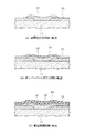
以下、本発明の一実施形態を図1乃至図3に基づいて説明する。まず、図3(b)に基づいて、本実施形態の製造方法で製造した厚膜抵抗体印刷基板の構造を説明する。セラミック基板11は、800℃〜1000℃で焼成する低温焼成セラミック基板、又は、1600℃前後で焼成するアルミナ基板、AlN基板等、いずれのセラミック基板であっても良く、また、多層基板、単層基板のいずれであっても良い。このセラミック基板11の表面には、厚膜抵抗体12を接続するための電極パターン13が印刷・焼成されている。本実施形態では、電極パターン13は、Cu導体ペーストで形成されているが、Ag、Ag/Pd、Ag/Pt等のAg系導体やAu系導体等の他の低融点金属ペーストを用いても良い。
【0011】
更に、セラミック基板11の表面には、電極パターン13に跨がって厚膜抵抗体12が印刷・焼成されている。この厚膜抵抗体12は、RuO2 系やSnO2系等の厚膜抵抗体ペーストで形成されている。この厚膜抵抗体12と電極パターン13の表面には、オーバーコートガラス14が印刷・焼成され、厚膜抵抗体12と電極パターン13の表面がオーバーコートガラス14で覆われている。
【0012】
更に、オーバーコートガラス14の表面には、絶縁性の樹脂被膜15がオーバーコートガラス14の表面全体又は少なくとも厚膜抵抗体12全体を覆うように形成されている。この樹脂被膜15は、紫外線硬化型の樹脂(感光性樹脂)を用いて形成されている。そして、樹脂被膜15、オーバーコートガラス14及び厚膜抵抗体12には、これら三者を貫通するトリミング溝16がレーザトリミング等のトリミングによって形成され、このトリミング溝16によって厚膜抵抗体12の抵抗値が調整されている。そして、このトリミング溝16には、樹脂被膜15と同じ紫外線硬化型の樹脂(感光性樹脂)がスクリーン印刷によって充填され、この充填樹脂17によってトリミング溝16が封止されている。
【0013】
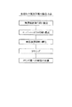
次に、上記構成の厚膜抵抗体印刷基板の製造方法を図1乃至図3を用いて説明する。ここで、図1は、厚膜抵抗体12の印刷・焼成工程から最終工程までの各工程を示す工程フローチャートであり、図2及び図3は、各工程の作業内容を示す縦断面図である。
【0014】
厚膜抵抗体12を印刷する前に、予め、セラミック基板11の表面に電極パターン13をスクリーン印刷して焼成しておく。尚、セラミック基板11の焼成後に電極パターン13を後付けで印刷・焼成しても良いが、セラミック基板11が低温焼成セラミック基板である場合には、セラミック基板11と電極パターン13等の表層導体パターンとを同時焼成するようにしても良い。この際、電極パターン13としてCu導体を用いる場合は、酸化防止のために還元雰囲気(窒素ガス)中で焼成する必要があるが、Ag系導体やAu系導体を用いた場合には、酸化雰囲気(空気)中で焼成することが可能である。
【0015】
電極パターン13の焼成後、図2(a)に示すように、セラミック基板11の表面にRuO2 系やSnO2 系等の厚膜抵抗体12のペーストを電極パターン13に跨がってスクリーン印刷し、これを焼成する。この際、厚膜抵抗体12の焼成温度は、セラミック基板11の焼成温度よりも僅かに低い温度に設定することが好ましいが、セラミック基板11の焼成温度とほぼ同じ温度で厚膜抵抗体12を焼成しても良い。
【0016】
この後、図2(b)に示すように、厚膜抵抗体12及び電極パターン13の表面に、オーバーコートガラス14のペーストをスクリーン印刷し、これを厚膜抵抗体12の焼成温度よりも低い温度(例えば600〜700℃)で焼成する。オーバーコートガラス14のペーストは、硼珪酸ガラス等のガラス粉末に有機バインダと溶剤を加えて混練したものである。尚、厚膜抵抗体12とオーバーコートガラス14は、同時焼成するようにしても良い。
【0017】
オバーコートガラス14の焼成後、図2(c)に示すように、オーバーコートガラス14の表面に、紫外線硬化型の絶縁性樹脂(感光性樹脂)のペーストを用いて樹脂被膜15をスクリーン印刷する。使用する紫外線硬化型の絶縁性樹脂は、例えば感光性エポキシ樹脂を用いれば良い。尚、樹脂被膜15の印刷範囲はオーバーコートガラス14の表面全体であっても良いが、厚膜抵抗体12全体を覆うだけの部分的な印刷であっても良い。樹脂被膜15の印刷後、樹脂被膜15に紫外線を照射して硬化させる。
【0018】
樹被膜15の硬化後、図3(a)に示すように、厚膜抵抗体12の抵抗値を調整するために、樹脂被膜15の上から厚膜抵抗体12をレーザトリミング等でトリミングして、樹脂被膜15、オーバーコートガラス14及び厚膜抵抗体12を貫通する抵抗値調整用のトリミング溝16を形成する。
【0019】
トミング後、図3(b)に示すように、トリミング溝16に、厚膜抵抗体12と同じ紫外線硬化型の絶縁性樹脂(感光性樹脂)をスクリーン印刷により充填し、この充填樹脂17でトリミング溝16を封止する。そして、最後に、この充填樹脂17に紫外線を照射して硬化させる。これにより、厚膜抵抗体印刷基板が完成する。
【0020】
以上説明した本実施形態の厚膜抵抗体印刷基板の製造方法によれば、トリミング前に、オーバーコートガラス14の表面に樹脂被膜15を形成するので、トリミング時に発生するミストの影響を全く受けずに、樹脂被膜15を形成することができ、トリミング溝16の周辺の樹脂被膜15にトリミング時のミストによるピンホールが全く発生しない。また、トリミング後に、トリミング溝16を充填樹脂17で穴埋めするので、厚膜抵抗体12をオーバーコートガラス14、樹脂被膜15、充填樹脂17によって完全に封止することができ、耐湿性、信頼性を向上することができる。
【0021】
本発明者らは、本実施形態の製造方法による樹脂被膜15のピンホール発生防止効果を評価するために、本実施形態の製造方法(図1乃至図3と従来の製造方法(図5及び図6)で、それぞれ、樹脂被膜とオーバーコートガラスで覆われた厚膜抵抗体を1000箇所ずつ形成してトリミングし、トリミング溝周辺の樹脂被膜に発生したピンホールの発生数を測定したところ、従来の製造方法では、1000箇所のサンプルの全てにピンホールが発生し、ピンホール発生率が100%であった。これに対し、本実施形態の製造方法では、1000箇所のサンプル中にピンホールが発生したサンプルは皆無であり、ピンホール発生率が0%であった。この試験結果からも、本実施形態の製造方法による優れたピンホール発生防止効果が確認された。
【0022】
また、本実施形態では、樹脂被膜15と充填樹脂17を紫外線硬化型の樹脂(感光性樹脂)を用いて形成するようにしたので、熱硬化型の樹脂と比較して、樹脂の硬化処理が容易であり、生産性も向上できる。しかも、紫外線硬化型の樹脂は、加熱する必要がないため、樹脂の硬化時に基板表面の導体パターンの酸化が発生しないという利点もある。
【0023】
尚、樹脂被膜15と充填樹脂17は、異なる樹脂で形成しても良い。また、樹脂被膜15と充填樹脂17を形成する樹脂は、紫外線照射と加熱を併用するタイプの樹脂を用いても良く、この場合でも、熱硬化型樹脂と比べて、加熱温度が低く、加熱時間も短時間で良いため、基板表面の導体パターンの酸化を抑制することができる。
【0024】
【発明の効果】
以上の説明から明らかなように、本発明の厚膜抵抗体印刷基板の製造方法によれば、トリミング前に、オーバーコートガラスの表面に樹脂被膜を形成して、この樹脂被膜の上から厚膜抵抗体をトリミングした後に、トリミング溝を絶縁性の樹脂で穴埋めすることができるので、トリミング後の厚膜抵抗体の表面をピンホールのない樹脂被膜によって完全に覆うことができて耐湿性を向上することができ、電気的特性の安定した信頼性の高い厚膜抵抗体を形成することができる。
【0025】
しかも、樹脂被膜と充填樹脂を紫外線硬化型の樹脂(感光性樹脂)を用いて形成するようにしたので、熱硬化型の樹脂と比較して、樹脂の硬化処理が容易で、生産性を向上できると共に、樹脂の硬化時に基板表面の導体パターンの酸化が発生せず、導体パターンの特性を良好に維持することができる。
【図面の簡単な説明】
【図1】本発明の一実施形態における厚膜抵抗体印刷基板の製造工程を示す工程フローチャート
【図2】(a)は厚膜抵抗体印刷・焼成工程の作業内容を示す縦断面図、(b)はオーバーコートガラス印刷・焼成工程の作業内容を示す縦断面図、(c)は樹脂被膜印刷・硬化工程の作業内容を示す縦断面図
【図3】(a)はトリミング工程の作業内容を示す縦断面図、(b)はトリミング溝への樹脂の充填工程の作業内容を示す縦断面図
【図4】従来の厚膜抵抗体印刷基板の構造を説明する縦断面図
【図5】従来の厚膜抵抗体印刷基板の製造工程を示す工程フローチャート
【図6】従来の厚膜抵抗体印刷基板の製造工程を説明するための図であり、(a)はオーバーコートガラス印刷・焼成工程の作業内容を示す縦断面図、(b)はトリミング工程の作業内容を示す縦断面図、(c)は樹脂被膜印刷・硬化工程の作業内容を示す縦断面図
【符号の説明】
11…セラミック基板、12…厚膜抵抗体、13…電極パターン、14…オーバーコートガラス、15…樹脂被膜、16…トリミング溝、17…充填樹脂。[0001]
BACKGROUND OF THE INVENTION
The present invention relates to a method for manufacturing thick film resistor printing in which an overcoat glass and a resin film are overlaid on the surface of a thick film resistor formed on a substrate surface.
[0002]
[Prior art]
In recent years, as shown in Japanese Patent Application Laid-Open No. 10-154868 (see FIG. 4), in order to improve the moisture resistance of the
[0003]
Generally, since the resistance value of the fired
[0004]
Therefore, as shown in FIGS. 5 and 6A, the
[0005]
[Problems to be solved by the invention]
In the above conventional manufacturing method, after the
[0006]
The present invention has been made in view of such circumstances. Accordingly, the object of the present invention is to completely cover the surface of the thick film resistor after trimming with a resin film having no pinhole, thereby improving moisture resistance. It is an object of the present invention to provide a method for manufacturing a thick film resistor printed circuit board that can be improved and can form a highly reliable thick film resistor with stable electrical characteristics.
[0007]
[Means for Solving the Problems]
In order to achieve the above object, a method of manufacturing a thick film resistor printed circuit board according to the present invention comprises a step of forming a thick film resistor on a substrate surface, and a surface of the thick film resistor as in
[0008]
According to this manufacturing method, since the resin film is formed on the surface of the overcoat glass before trimming, the resin film can be formed without being affected by mist generated at the time of trimming. No pinhole due to mist at the time of trimming occurs in the resin film. In addition, after trimming, the trimming groove is filled with an insulating resin, so that the thick film resistor can be completely sealed with overcoat glass, resin coating, and filling resin, and moisture resistance and reliability are improved. Can do.
[0009]
In this case, the resin film and the filling resin are preferably formed using an ultraviolet curable resin (photosensitive resin). In general, UV curable resins have higher moisture barrier properties and superior moisture resistance compared to overcoated glass that has been printed and baked with a glass paste. Can be easily cured, and productivity can be improved. Moreover, since the ultraviolet curable resin does not need to be heated, the conductor pattern on the substrate surface is not oxidized during the curing of the resin. Incidentally, since it is necessary to heat the thermosetting resin at about 120 to 150 ° C., for example, for about 30 to 50 minutes at the time of curing, the conductor pattern on the substrate surface is oxidized during the heat curing of the resin, so The characteristic will change.
[0010]
DETAILED DESCRIPTION OF THE INVENTION
Hereinafter, an embodiment of the present invention will be described with reference to FIGS. 1 to 3. First, based on FIG.3 (b), the structure of the thick film resistor printed circuit board manufactured with the manufacturing method of this embodiment is demonstrated. The
[0011]
Further, a
[0012]
Furthermore, an
[0013]
Next, a method of manufacturing the thick film resistor printed circuit board having the above configuration will be described with reference to FIGS. Here, FIG. 1 is a process flowchart showing each process from the printing / baking process to the final process of the
[0014]
Before printing the
[0015]
After firing the
[0016]
Thereafter, as shown in FIG. 2B, the paste of the
[0017]
After firing the
[0018]
After the
[0019]
After the tomming, as shown in FIG. 3B, the trimming
[0020]
According to the method for manufacturing the thick film resistor printed board of the present embodiment described above, the
[0021]
In order to evaluate the pinhole generation prevention effect of the
[0022]
In this embodiment, since the
[0023]
The
[0024]
【The invention's effect】
As is clear from the above description, according to the method for manufacturing a thick film resistor printed board of the present invention, a resin film is formed on the surface of the overcoat glass before trimming, and the thick film is formed on the resin film. After trimming the resistor, the trimming groove can be filled with an insulating resin, so the surface of the thick film resistor after trimming can be completely covered with a resin film without pinholes, improving moisture resistance. Therefore, a highly reliable thick film resistor with stable electrical characteristics can be formed.
[0025]
In addition, since the resin coating and filling resin are formed using an ultraviolet curable resin (photosensitive resin), the resin curing process is easier and productivity is improved compared to thermosetting resins. In addition, the conductive pattern on the substrate surface is not oxidized during the curing of the resin, and the characteristics of the conductive pattern can be maintained well.
[Brief description of the drawings]
FIG. 1 is a process flow chart showing a manufacturing process of a thick film resistor printed circuit board according to an embodiment of the present invention. FIG. 2A is a longitudinal sectional view showing work contents of a thick film resistor printing / firing process. b) Longitudinal sectional view showing the work contents of the overcoat glass printing / firing process, (c) Longitudinal sectional view showing the work contents of the resin film printing / curing process. [FIG. 3] (a) is the work contents of the trimming process. FIG. 4B is a longitudinal cross-sectional view illustrating the work content of the resin filling process into the trimming groove. FIG. 4 is a longitudinal cross-sectional view illustrating the structure of a conventional thick film resistor printed circuit board. FIG. 6 is a process flow chart showing a conventional thick film resistor printed circuit board manufacturing process. FIG. 6 is a diagram for explaining a conventional thick film resistor printed circuit board manufacturing process. FIG. The longitudinal cross-sectional view which shows the work content of (b) is Trimin Longitudinal sectional view showing a work process, (c) vertical sectional view showing the work of the resin coating printing and curing step EXPLANATION OF REFERENCE NUMERALS
DESCRIPTION OF
Claims (2)
Priority Applications (1)
| Application Number | Priority Date | Filing Date | Title |
|---|---|---|---|
| JP2000111905A JP4395980B2 (en) | 2000-04-07 | 2000-04-07 | Method for manufacturing thick film resistor printed circuit board |
Applications Claiming Priority (1)
| Application Number | Priority Date | Filing Date | Title |
|---|---|---|---|
| JP2000111905A JP4395980B2 (en) | 2000-04-07 | 2000-04-07 | Method for manufacturing thick film resistor printed circuit board |
Publications (2)
| Publication Number | Publication Date |
|---|---|
| JP2001291603A JP2001291603A (en) | 2001-10-19 |
| JP4395980B2 true JP4395980B2 (en) | 2010-01-13 |
Family
ID=18624168
Family Applications (1)
| Application Number | Title | Priority Date | Filing Date |
|---|---|---|---|
| JP2000111905A Expired - Lifetime JP4395980B2 (en) | 2000-04-07 | 2000-04-07 | Method for manufacturing thick film resistor printed circuit board |
Country Status (1)
| Country | Link |
|---|---|
| JP (1) | JP4395980B2 (en) |
Families Citing this family (2)
| Publication number | Priority date | Publication date | Assignee | Title |
|---|---|---|---|---|
| JP2004140117A (en) * | 2002-10-16 | 2004-05-13 | Hitachi Ltd | Multilayer circuit board, and method of manufacturing the same |
| JP4746594B2 (en) * | 2007-07-30 | 2011-08-10 | 住友電気工業株式会社 | Printed wiring board and manufacturing method thereof |
-
2000
- 2000-04-07 JP JP2000111905A patent/JP4395980B2/en not_active Expired - Lifetime
Also Published As
| Publication number | Publication date |
|---|---|
| JP2001291603A (en) | 2001-10-19 |
Similar Documents
| Publication | Publication Date | Title |
|---|---|---|
| KR900008274B1 (en) | Thick film resistor circuits | |
| WO2003046934A1 (en) | Chip resistor and method for producing the same | |
| JPH07106729A (en) | Manufacture of thick film circuit component | |
| JPH11204304A (en) | Resistor and its manufacture | |
| JP4395980B2 (en) | Method for manufacturing thick film resistor printed circuit board | |
| JPH0312789B2 (en) | ||
| JPH02110903A (en) | Manufacture of resistor | |
| JP2641530B2 (en) | Manufacturing method of chip-shaped electronic component | |
| JP2515202B2 (en) | Ceramic wiring board and manufacturing method thereof | |
| JP3092451B2 (en) | Rectangular thin film chip resistor and method of manufacturing the same | |
| JPS6025294A (en) | Method of producing circuit board | |
| JP3460384B2 (en) | Composite electronic component and method of manufacturing the same | |
| JP2718178B2 (en) | Manufacturing method of square plate type thin film chip resistor | |
| JP3837060B2 (en) | Manufacturing method of chip resistor | |
| JP2718232B2 (en) | Manufacturing method of square plate type thin film chip resistor | |
| JP2718196B2 (en) | Manufacturing method of square plate type thin film chip resistor | |
| JPS5918669A (en) | Formation of thick film circuit | |
| JPH08321402A (en) | Chip-like electronic part and its production | |
| JPH04128055A (en) | Electronic circuit device and its manufacture | |
| JPH04326702A (en) | Electronic component | |
| JPH02129997A (en) | Manufacture of multilayer ceramic circuit substrate | |
| JPH05234726A (en) | Formation method of thick film resistor circuit | |
| JPH03109793A (en) | Manufacture of wiring circuit board with resistor | |
| JPH02273986A (en) | Thick film circuit board | |
| JPH04334083A (en) | Thick film circuit board and its manufacture |
Legal Events
| Date | Code | Title | Description |
|---|---|---|---|
| RD02 | Notification of acceptance of power of attorney |
Free format text: JAPANESE INTERMEDIATE CODE: A7422 Effective date: 20040623 |
|
| A621 | Written request for application examination |
Free format text: JAPANESE INTERMEDIATE CODE: A621 Effective date: 20061220 |
|
| A977 | Report on retrieval |
Free format text: JAPANESE INTERMEDIATE CODE: A971007 Effective date: 20080919 |
|
| A131 | Notification of reasons for refusal |
Free format text: JAPANESE INTERMEDIATE CODE: A131 Effective date: 20080930 |
|
| A521 | Written amendment |
Free format text: JAPANESE INTERMEDIATE CODE: A523 Effective date: 20081126 |
|
| TRDD | Decision of grant or rejection written | ||
| A01 | Written decision to grant a patent or to grant a registration (utility model) |
Free format text: JAPANESE INTERMEDIATE CODE: A01 Effective date: 20090929 |
|
| A01 | Written decision to grant a patent or to grant a registration (utility model) |
Free format text: JAPANESE INTERMEDIATE CODE: A01 |
|
| A61 | First payment of annual fees (during grant procedure) |
Free format text: JAPANESE INTERMEDIATE CODE: A61 Effective date: 20091012 |
|
| FPAY | Renewal fee payment (event date is renewal date of database) |
Free format text: PAYMENT UNTIL: 20121030 Year of fee payment: 3 |
|
| R150 | Certificate of patent or registration of utility model |
Ref document number: 4395980 Country of ref document: JP Free format text: JAPANESE INTERMEDIATE CODE: R150 Free format text: JAPANESE INTERMEDIATE CODE: R150 |
|
| FPAY | Renewal fee payment (event date is renewal date of database) |
Free format text: PAYMENT UNTIL: 20131030 Year of fee payment: 4 |
|
| EXPY | Cancellation because of completion of term |