JP4314887B2 - 窒化物半導体素子 - Google Patents
窒化物半導体素子 Download PDFInfo
- Publication number
- JP4314887B2 JP4314887B2 JP2003148359A JP2003148359A JP4314887B2 JP 4314887 B2 JP4314887 B2 JP 4314887B2 JP 2003148359 A JP2003148359 A JP 2003148359A JP 2003148359 A JP2003148359 A JP 2003148359A JP 4314887 B2 JP4314887 B2 JP 4314887B2
- Authority
- JP
- Japan
- Prior art keywords
- nitride semiconductor
- layer
- semiconductor layer
- crystal defects
- grown
- Prior art date
- Legal status (The legal status is an assumption and is not a legal conclusion. Google has not performed a legal analysis and makes no representation as to the accuracy of the status listed.)
- Expired - Lifetime
Links
Images


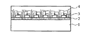


Landscapes
- Semiconductor Lasers (AREA)
Priority Applications (1)
| Application Number | Priority Date | Filing Date | Title |
|---|---|---|---|
| JP2003148359A JP4314887B2 (ja) | 1997-11-26 | 2003-05-26 | 窒化物半導体素子 |
Applications Claiming Priority (2)
| Application Number | Priority Date | Filing Date | Title |
|---|---|---|---|
| JP32499797 | 1997-11-26 | ||
| JP2003148359A JP4314887B2 (ja) | 1997-11-26 | 2003-05-26 | 窒化物半導体素子 |
Related Parent Applications (1)
| Application Number | Title | Priority Date | Filing Date |
|---|---|---|---|
| JP13283198A Division JP3456413B2 (ja) | 1997-11-26 | 1998-05-15 | 窒化物半導体の成長方法及び窒化物半導体素子 |
Publications (3)
| Publication Number | Publication Date |
|---|---|
| JP2004006886A JP2004006886A (ja) | 2004-01-08 |
| JP2004006886A5 JP2004006886A5 (https=) | 2005-09-22 |
| JP4314887B2 true JP4314887B2 (ja) | 2009-08-19 |
Family
ID=30445545
Family Applications (1)
| Application Number | Title | Priority Date | Filing Date |
|---|---|---|---|
| JP2003148359A Expired - Lifetime JP4314887B2 (ja) | 1997-11-26 | 2003-05-26 | 窒化物半導体素子 |
Country Status (1)
| Country | Link |
|---|---|
| JP (1) | JP4314887B2 (https=) |
Families Citing this family (2)
| Publication number | Priority date | Publication date | Assignee | Title |
|---|---|---|---|---|
| CN100533794C (zh) * | 2003-02-07 | 2009-08-26 | 三洋电机株式会社 | 半导体元件 |
| CN117401997B (zh) * | 2023-11-01 | 2024-09-20 | 郑州宏拓精密工具有限公司 | 一种光伏籽晶掏刀及其制备方法 |
Family Cites Families (8)
| Publication number | Priority date | Publication date | Assignee | Title |
|---|---|---|---|---|
| JP3974667B2 (ja) * | 1994-08-22 | 2007-09-12 | ローム株式会社 | 半導体発光素子の製法 |
| JP2828002B2 (ja) * | 1995-01-19 | 1998-11-25 | 松下電器産業株式会社 | 半導体発光素子およびその製造方法 |
| DE69622277T2 (de) * | 1995-09-18 | 2003-03-27 | Hitachi, Ltd. | Halbleitermaterial, verfahren zur herstellung des halbleitermaterials und eine halbleitervorrichtung |
| JP3350855B2 (ja) * | 1995-10-16 | 2002-11-25 | 日本電信電話株式会社 | Iii族窒化物半導体基板の製造方法 |
| JP3139445B2 (ja) * | 1997-03-13 | 2001-02-26 | 日本電気株式会社 | GaN系半導体の成長方法およびGaN系半導体膜 |
| JPH1143398A (ja) * | 1997-07-22 | 1999-02-16 | Mitsubishi Cable Ind Ltd | GaN系結晶成長用基板およびその用途 |
| JP3925753B2 (ja) * | 1997-10-24 | 2007-06-06 | ソニー株式会社 | 半導体素子およびその製造方法ならびに半導体発光素子 |
| JPH11135882A (ja) * | 1997-10-28 | 1999-05-21 | Sharp Corp | 化合物半導体基板、及び化合物半導体基板の製造方法、並びに発光素子 |
-
2003
- 2003-05-26 JP JP2003148359A patent/JP4314887B2/ja not_active Expired - Lifetime
Also Published As
| Publication number | Publication date |
|---|---|
| JP2004006886A (ja) | 2004-01-08 |
Similar Documents
| Publication | Publication Date | Title |
|---|---|---|
| US7442254B2 (en) | Nitride semiconductor device having a nitride semiconductor substrate and an indium containing active layer | |
| JP3456413B2 (ja) | 窒化物半導体の成長方法及び窒化物半導体素子 | |
| JP4378070B2 (ja) | 窒化物半導体素子 | |
| JP3669848B2 (ja) | 窒化物半導体レーザ素子 | |
| JP3876518B2 (ja) | 窒化物半導体基板の製造方法および窒化物半導体基板 | |
| JP3436128B2 (ja) | 窒化物半導体の成長方法及び窒化物半導体素子 | |
| JPH11191657A (ja) | 窒化物半導体の成長方法及び窒化物半導体素子 | |
| JPH11191659A (ja) | 窒化物半導体の成長方法及び窒化物半導体素子 | |
| JP2001203385A (ja) | 窒化物半導体発光ダイオード | |
| JP3651260B2 (ja) | 窒化物半導体素子 | |
| JP4043087B2 (ja) | 窒化物半導体素子の製造方法及び窒化物半導体素子 | |
| JP4337132B2 (ja) | 窒化物半導体基板及びそれを用いた窒化物半導体素子 | |
| JP3847000B2 (ja) | 窒化物半導体基板上に活性層を備えた窒化物半導体層を有する窒化物半導体素子及びその成長方法 | |
| JP2008034862A (ja) | 窒化物半導体の成長方法 | |
| JP4628651B2 (ja) | 窒化物半導体発光素子の製造方法 | |
| JPH10290047A (ja) | 窒化物半導体素子 | |
| JPH11330622A (ja) | 窒化物半導体素子 | |
| JP3216118B2 (ja) | 窒化物半導体素子及びその製造方法 | |
| JP4637503B2 (ja) | 窒化物半導体レーザ素子の製造方法 | |
| JP4314887B2 (ja) | 窒化物半導体素子 | |
| JP2001024223A (ja) | 窒化物半導体発光ダイオード | |
| JP2003249463A5 (https=) | ||
| JP4524997B2 (ja) | 窒化物半導体素子 | |
| JP2002151798A (ja) | 窒化物半導体素子 | |
| JP2002151798A5 (https=) |
Legal Events
| Date | Code | Title | Description |
|---|---|---|---|
| A521 | Written amendment |
Free format text: JAPANESE INTERMEDIATE CODE: A523 Effective date: 20050418 |
|
| A621 | Written request for application examination |
Free format text: JAPANESE INTERMEDIATE CODE: A621 Effective date: 20050418 |
|
| A977 | Report on retrieval |
Free format text: JAPANESE INTERMEDIATE CODE: A971007 Effective date: 20070404 |
|
| A131 | Notification of reasons for refusal |
Free format text: JAPANESE INTERMEDIATE CODE: A131 Effective date: 20080311 |
|
| A521 | Written amendment |
Free format text: JAPANESE INTERMEDIATE CODE: A523 Effective date: 20080512 |
|
| TRDD | Decision of grant or rejection written | ||
| A01 | Written decision to grant a patent or to grant a registration (utility model) |
Free format text: JAPANESE INTERMEDIATE CODE: A01 Effective date: 20090428 |
|
| A01 | Written decision to grant a patent or to grant a registration (utility model) |
Free format text: JAPANESE INTERMEDIATE CODE: A01 |
|
| A61 | First payment of annual fees (during grant procedure) |
Free format text: JAPANESE INTERMEDIATE CODE: A61 Effective date: 20090511 |
|
| R150 | Certificate of patent or registration of utility model |
Free format text: JAPANESE INTERMEDIATE CODE: R150 |
|
| FPAY | Renewal fee payment (event date is renewal date of database) |
Free format text: PAYMENT UNTIL: 20120529 Year of fee payment: 3 |
|
| FPAY | Renewal fee payment (event date is renewal date of database) |
Free format text: PAYMENT UNTIL: 20120529 Year of fee payment: 3 |
|
| FPAY | Renewal fee payment (event date is renewal date of database) |
Free format text: PAYMENT UNTIL: 20120529 Year of fee payment: 3 |
|
| FPAY | Renewal fee payment (event date is renewal date of database) |
Free format text: PAYMENT UNTIL: 20120529 Year of fee payment: 3 |
|
| FPAY | Renewal fee payment (event date is renewal date of database) |
Free format text: PAYMENT UNTIL: 20130529 Year of fee payment: 4 |
|
| FPAY | Renewal fee payment (event date is renewal date of database) |
Free format text: PAYMENT UNTIL: 20130529 Year of fee payment: 4 |
|
| FPAY | Renewal fee payment (event date is renewal date of database) |
Free format text: PAYMENT UNTIL: 20140529 Year of fee payment: 5 |
|
| R157 | Certificate of patent or utility model (correction) |
Free format text: JAPANESE INTERMEDIATE CODE: R157 |
|
| R250 | Receipt of annual fees |
Free format text: JAPANESE INTERMEDIATE CODE: R250 |
|
| R250 | Receipt of annual fees |
Free format text: JAPANESE INTERMEDIATE CODE: R250 |
|
| R250 | Receipt of annual fees |
Free format text: JAPANESE INTERMEDIATE CODE: R250 |
|
| R250 | Receipt of annual fees |
Free format text: JAPANESE INTERMEDIATE CODE: R250 |
|
| EXPY | Cancellation because of completion of term |