JP4307322B2 - Radiation imaging apparatus and radiation imaging system - Google Patents
Radiation imaging apparatus and radiation imaging system Download PDFInfo
- Publication number
- JP4307322B2 JP4307322B2 JP2004148051A JP2004148051A JP4307322B2 JP 4307322 B2 JP4307322 B2 JP 4307322B2 JP 2004148051 A JP2004148051 A JP 2004148051A JP 2004148051 A JP2004148051 A JP 2004148051A JP 4307322 B2 JP4307322 B2 JP 4307322B2
- Authority
- JP
- Japan
- Prior art keywords
- photoelectric conversion
- bias
- circuit unit
- conversion element
- signal
- Prior art date
- Legal status (The legal status is an assumption and is not a legal conclusion. Google has not performed a legal analysis and makes no representation as to the accuracy of the status listed.)
- Expired - Fee Related
Links
- 238000003384 imaging method Methods 0.000 title claims description 81
- 230000005855 radiation Effects 0.000 title claims description 47
- 238000006243 chemical reaction Methods 0.000 claims description 276
- 229910021417 amorphous silicon Inorganic materials 0.000 claims description 18
- 230000005669 field effect Effects 0.000 claims description 16
- 239000000758 substrate Substances 0.000 claims description 12
- 239000010409 thin film Substances 0.000 claims description 12
- 238000002347 injection Methods 0.000 claims description 10
- 239000007924 injection Substances 0.000 claims description 10
- 239000004065 semiconductor Substances 0.000 claims description 10
- 229910052751 metal Inorganic materials 0.000 claims description 9
- 239000002184 metal Substances 0.000 claims description 9
- 230000000903 blocking effect Effects 0.000 claims description 8
- 239000000463 material Substances 0.000 claims description 7
- 230000000717 retained effect Effects 0.000 claims description 4
- HQVNEWCFYHHQES-UHFFFAOYSA-N silicon nitride Chemical compound N12[Si]34N5[Si]62N3[Si]51N64 HQVNEWCFYHHQES-UHFFFAOYSA-N 0.000 claims description 4
- 238000003860 storage Methods 0.000 claims description 4
- 230000003321 amplification Effects 0.000 claims description 3
- 238000003199 nucleic acid amplification method Methods 0.000 claims description 3
- 230000003287 optical effect Effects 0.000 claims description 2
- 230000005684 electric field Effects 0.000 claims 2
- 239000003990 capacitor Substances 0.000 description 21
- 238000010586 diagram Methods 0.000 description 11
- 238000000034 method Methods 0.000 description 8
- 239000010408 film Substances 0.000 description 7
- OAICVXFJPJFONN-UHFFFAOYSA-N Phosphorus Chemical compound [P] OAICVXFJPJFONN-UHFFFAOYSA-N 0.000 description 6
- 101100194362 Schizosaccharomyces pombe (strain 972 / ATCC 24843) res1 gene Proteins 0.000 description 6
- 230000008859 change Effects 0.000 description 6
- 239000000872 buffer Substances 0.000 description 5
- 230000003071 parasitic effect Effects 0.000 description 5
- 230000001678 irradiating effect Effects 0.000 description 4
- 238000004519 manufacturing process Methods 0.000 description 4
- XUIMIQQOPSSXEZ-UHFFFAOYSA-N Silicon Chemical compound [Si] XUIMIQQOPSSXEZ-UHFFFAOYSA-N 0.000 description 3
- 230000008901 benefit Effects 0.000 description 3
- 230000005540 biological transmission Effects 0.000 description 3
- 238000001514 detection method Methods 0.000 description 3
- 238000003745 diagnosis Methods 0.000 description 3
- 239000011159 matrix material Substances 0.000 description 3
- 229910052710 silicon Inorganic materials 0.000 description 3
- 239000010703 silicon Substances 0.000 description 3
- 229910004205 SiNX Inorganic materials 0.000 description 2
- 238000009825 accumulation Methods 0.000 description 2
- 238000002594 fluoroscopy Methods 0.000 description 2
- 239000012535 impurity Substances 0.000 description 2
- 238000001727 in vivo Methods 0.000 description 2
- 238000003672 processing method Methods 0.000 description 2
- JBRZTFJDHDCESZ-UHFFFAOYSA-N AsGa Chemical compound [As]#[Ga] JBRZTFJDHDCESZ-UHFFFAOYSA-N 0.000 description 1
- 229910001218 Gallium arsenide Inorganic materials 0.000 description 1
- BUGBHKTXTAQXES-UHFFFAOYSA-N Selenium Chemical compound [Se] BUGBHKTXTAQXES-UHFFFAOYSA-N 0.000 description 1
- 230000032683 aging Effects 0.000 description 1
- 239000000969 carrier Substances 0.000 description 1
- 238000001816 cooling Methods 0.000 description 1
- 239000013078 crystal Substances 0.000 description 1
- 230000002950 deficient Effects 0.000 description 1
- 238000002059 diagnostic imaging Methods 0.000 description 1
- 239000002019 doping agent Substances 0.000 description 1
- 230000000694 effects Effects 0.000 description 1
- 238000005516 engineering process Methods 0.000 description 1
- 229910052736 halogen Inorganic materials 0.000 description 1
- 150000002367 halogens Chemical class 0.000 description 1
- 230000020169 heat generation Effects 0.000 description 1
- XMBWDFGMSWQBCA-UHFFFAOYSA-N hydrogen iodide Chemical compound I XMBWDFGMSWQBCA-UHFFFAOYSA-N 0.000 description 1
- 230000001939 inductive effect Effects 0.000 description 1
- 238000007689 inspection Methods 0.000 description 1
- 230000007246 mechanism Effects 0.000 description 1
- QKEOZZYXWAIQFO-UHFFFAOYSA-M mercury(1+);iodide Chemical compound [Hg]I QKEOZZYXWAIQFO-UHFFFAOYSA-M 0.000 description 1
- 239000000203 mixture Substances 0.000 description 1
- ORQBXQOJMQIAOY-UHFFFAOYSA-N nobelium Chemical compound [No] ORQBXQOJMQIAOY-UHFFFAOYSA-N 0.000 description 1
- 238000002360 preparation method Methods 0.000 description 1
- 239000002994 raw material Substances 0.000 description 1
- 230000004044 response Effects 0.000 description 1
- 229910052711 selenium Inorganic materials 0.000 description 1
- 239000011669 selenium Substances 0.000 description 1
- 239000000126 substance Substances 0.000 description 1
- 230000001052 transient effect Effects 0.000 description 1
- 230000007704 transition Effects 0.000 description 1
Images


Classifications
-
- H—ELECTRICITY
- H04—ELECTRIC COMMUNICATION TECHNIQUE
- H04N—PICTORIAL COMMUNICATION, e.g. TELEVISION
- H04N5/00—Details of television systems
- H04N5/30—Transforming light or analogous information into electric information
- H04N5/32—Transforming X-rays
-
- H—ELECTRICITY
- H04—ELECTRIC COMMUNICATION TECHNIQUE
- H04N—PICTORIAL COMMUNICATION, e.g. TELEVISION
- H04N25/00—Circuitry of solid-state image sensors [SSIS]; Control thereof
- H04N25/30—Circuitry of solid-state image sensors [SSIS]; Control thereof for transforming X-rays into image signals
-
- H—ELECTRICITY
- H04—ELECTRIC COMMUNICATION TECHNIQUE
- H04N—PICTORIAL COMMUNICATION, e.g. TELEVISION
- H04N25/00—Circuitry of solid-state image sensors [SSIS]; Control thereof
- H04N25/60—Noise processing, e.g. detecting, correcting, reducing or removing noise
- H04N25/63—Noise processing, e.g. detecting, correcting, reducing or removing noise applied to dark current
-
- H—ELECTRICITY
- H04—ELECTRIC COMMUNICATION TECHNIQUE
- H04N—PICTORIAL COMMUNICATION, e.g. TELEVISION
- H04N25/00—Circuitry of solid-state image sensors [SSIS]; Control thereof
- H04N25/70—SSIS architectures; Circuits associated therewith
- H04N25/709—Circuitry for control of the power supply
-
- H—ELECTRICITY
- H04—ELECTRIC COMMUNICATION TECHNIQUE
- H04N—PICTORIAL COMMUNICATION, e.g. TELEVISION
- H04N25/00—Circuitry of solid-state image sensors [SSIS]; Control thereof
- H04N25/70—SSIS architectures; Circuits associated therewith
- H04N25/71—Charge-coupled device [CCD] sensors; Charge-transfer registers specially adapted for CCD sensors
- H04N25/75—Circuitry for providing, modifying or processing image signals from the pixel array
-
- H—ELECTRICITY
- H04—ELECTRIC COMMUNICATION TECHNIQUE
- H04N—PICTORIAL COMMUNICATION, e.g. TELEVISION
- H04N25/00—Circuitry of solid-state image sensors [SSIS]; Control thereof
- H04N25/70—SSIS architectures; Circuits associated therewith
- H04N25/76—Addressed sensors, e.g. MOS or CMOS sensors
- H04N25/78—Readout circuits for addressed sensors, e.g. output amplifiers or A/D converters
Landscapes
- Engineering & Computer Science (AREA)
- Multimedia (AREA)
- Signal Processing (AREA)
- Solid State Image Pick-Up Elements (AREA)
- Measurement Of Radiation (AREA)
- Apparatus For Radiation Diagnosis (AREA)
- Transforming Light Signals Into Electric Signals (AREA)
- Light Receiving Elements (AREA)
Description
本発明は、医療用の診断や工業用の非破壊検査等に用いて好適な放射線撮像装置及び放射線撮像システムに関する。なお、本発明においては、X線、γ線などの電磁波やα線、β線も放射線に含めるものとする。 The present invention relates to a radiation imaging apparatus and a radiation imaging system suitable for use in medical diagnosis, industrial nondestructive inspection, and the like. In the present invention, electromagnetic waves such as X-rays and γ rays, α rays, and β rays are also included in the radiation.
従来、病院内などに設置されているX線撮影システムには、患者にX線を照射し、患者を透過したX線をフィルムに露光するフィルム撮影方式と、患者を透過したX線を電気信号に変換してディジタル画像処理を行う画像処理方式とがある。画像処理方式を実現するひとつの装置として、X線を可視光に変換する蛍光体と可視光を電気信号に変換する光電変換装置とを備えた放射線撮像装置がある。患者を透過したX線が蛍光体に照射され、蛍光体で可視光に変換された患者の体内情報を光電変換装置により電気信号として出力する。患者の体内情報が電気信号に変換されれば、その電気信号をADコンバータでディジタル変換し、記録、表示、印刷、診断などを行うためのX線画像情報をディジタル値として扱うことができる。 Conventionally, in an X-ray imaging system installed in a hospital or the like, a film imaging system for irradiating a patient with X-rays and exposing the X-rays transmitted through the patient to a film, and an X-ray transmitted through the patient as an electrical signal There is an image processing method in which digital image processing is performed after conversion into a digital image. One apparatus that realizes an image processing method is a radiation imaging apparatus that includes a phosphor that converts X-rays into visible light and a photoelectric conversion device that converts visible light into electrical signals. X-rays transmitted through the patient are irradiated onto the phosphor, and the in-vivo information of the patient converted into visible light by the phosphor is output as an electrical signal by the photoelectric conversion device. If the in-vivo information of the patient is converted into an electrical signal, the electrical signal is digitally converted by an AD converter, and X-ray image information for recording, display, printing, diagnosis, etc. can be handled as a digital value.
最近では、光電変換装置にアモルファスシリコン半導体薄膜を用いた放射線撮像装置が実用化されている。 Recently, a radiation imaging apparatus using an amorphous silicon semiconductor thin film for a photoelectric conversion device has been put into practical use.
図11は、例えば特開平8−116044号公報(特許文献1)に開示されたMIS型光電変換素子とスイッチ素子の材料にアモルファスシリコン半導体薄膜を用いて構成した従来の光電変換基板を示す上面図であり、それらを結線する配線を含めて表している。図12は、図11中のI−I線に沿った断面図である。 FIG. 11 is a top view showing a conventional photoelectric conversion substrate configured by using an amorphous silicon semiconductor thin film as a material for a MIS type photoelectric conversion element and a switch element disclosed in, for example, Japanese Patent Laid-Open No. 8-116044 (Patent Document 1). It is shown including the wiring that connects them. 12 is a cross-sectional view taken along the line II in FIG.
光電変換素子101及びスイッチ素子102(アモルファスシリコンTFT、以下単にTFTと記す)は同一基板103上に形成されており、光電変換素子の下部電極は、TFTの下部電極(ゲート電極)と同一の第1の金属薄膜層104で共有されており、光電変換素子の上部電極は、TFTの上部電極(ソース電極、ドレイン電極)と同一の第2の金属薄膜層105で共有されている。また、第1及び第2の金属薄膜層は、光電変換回路部内の、ゲート駆動用配線106、マトリクス信号配線107も共有している。図12においては、画素数として2×2の計4画素分が記載されている。図12のハッチング部は、光電変換素子の受光面である。109は光電変換素子にバイアスを与える電源ラインである。また、110は光電変換素子とTFTを接続するためのコンタクトホールである。
The
アモルファスシリコン半導体を主たる材料にした図11で示されるような構成を用いれば、光電変換素子、スイッチ素子、ゲート駆動用配線、マトリクス信号配線を、同一基板上に同時に作製することができ、大面積の光電変換回路部が容易に、しかも安価に提供することができる。 If the structure as shown in FIG. 11 using an amorphous silicon semiconductor as a main material is used, a photoelectric conversion element, a switch element, a gate driving wiring, and a matrix signal wiring can be simultaneously manufactured on the same substrate, and a large area is obtained. This photoelectric conversion circuit portion can be provided easily and inexpensively.
次に、光電変換素子単体のデバイス動作について説明する。図13(a)〜(c)は、図11及び図12に示す光電変換素子のデバイス動作を説明するためのエネルギーバンド図である。本光電変換素子には、第1及び第2の金属薄膜層104及び105への電圧の印加の仕方によりリフレッシュモードと光電変換モードという2種類の動作モードがある。
Next, device operation of a single photoelectric conversion element will be described. FIGS. 13A to 13C are energy band diagrams for explaining the device operation of the photoelectric conversion element shown in FIGS. 11 and 12. This photoelectric conversion element has two types of operation modes, a refresh mode and a photoelectric conversion mode, depending on how the voltage is applied to the first and second metal
図13(a)、(b)は、それぞれリフレッシュモード、光電変換モードの動作を示しており、図12で示される各層の膜厚方向の状態を表している。M1は第1の金属薄膜層104(例えばCr)で形成された下部電極(G電極)である。アモルファス窒化シリコン(a−SiNx)層111は、電子、ホール共にその通過を阻止する絶縁層であり、トンネル効果をもたらさない程度の厚さが必要であり、通常500オングストローム以上に設定される。水素化アモルファスシリコン(a−Si:H)層112は意図的にドーパントをドープしていない真性半導体層(i層)で形成された光電変換半導体層である。N+層113は、a−Si:H層112へのホールの注入を阻止するために形成されたN型a−Si:H層等の非単結晶半導体からなる単一導電型キャリアの注入阻止層である。また、M2は第2金属薄膜層105(例えばAl)で形成される上部電極(D電極)である。
FIGS. 13A and 13B show the operation in the refresh mode and the photoelectric conversion mode, respectively, and show the state in the film thickness direction of each layer shown in FIG. M1 is a lower electrode (G electrode) formed of the first metal thin film layer 104 (for example, Cr). The amorphous silicon nitride (a-SiNx)
図14は、光電変換素子及びスイッチ素子の材料にアモルファスシリコン半導体薄膜を用いて構成した従来の光電変換基板の2次元的構成を示す回路図である。但し、説明を簡単化するために3×3=9画素分で記載してある。 FIG. 14 is a circuit diagram showing a two-dimensional configuration of a conventional photoelectric conversion substrate configured using an amorphous silicon semiconductor thin film as a material for the photoelectric conversion element and the switch element. However, for simplification of description, 3 × 3 = 9 pixels are shown.
図14において、S1−1〜S3−3は光電変換素子、T1−1〜T3−3はスイッチ素子(TFT:Thin Film Transistor)、G1〜G3はTFTをオン/オフさせるためのゲート配線、M1〜M3は信号配線、Vs線は光電変換素子に蓄積バイアスを与えるための配線である。各光電変換素子S1−1〜S3−3の黒く塗りつぶされた側の電極はG電極であり、対向側はD電極である。D電極は、Vs線の一部と接続されているが、光を入射させる都合上、例えば、薄いN+層がD電極として使用される。この従来例では、光電変換素子S1−1〜S3−3、スイッチ素子T1−1〜T3−3、ゲート配線G1〜G3、信号配線M1〜M3及びVs線が光電変換回路部701に含まれている。Vs線は、電源Vsによりバイアスされる。SR1はゲート配線G1〜G3に駆動用のパルス電圧を与えるシフトレジスタであり、TFTをオンさせる電圧Vcomは外部から供給さる。また、制御信号VSCは、光電変換素子のVs線、即ち光電変換素子のD電極に、2種類のバイアスを与えるためのものである。D電極は、制御信号VSCが“Hi”の時にVref(V)になり、“Lo”の時にVs(V)になる。読み取り用電源Vs(V)、リフレッシュ用電源Vref(V)は、夫々直流電源であり、例えば、Vsは9V、Vrefは3Vとする。 In FIG. 14, S1-1 to S3-3 are photoelectric conversion elements, T1-1 to T3-3 are switch elements (TFTs), G1 to G3 are gate wirings for turning on / off the TFTs, M1 ˜M3 are signal wirings, and the Vs line is a wiring for applying a storage bias to the photoelectric conversion element. The electrodes on the sides of the photoelectric conversion elements S1-1 to S3-3 that are painted black are G electrodes, and the opposite side is a D electrode. The D electrode is connected to a part of the Vs line, but for convenience of entering light, for example, a thin N + layer is used as the D electrode. In this conventional example, photoelectric conversion elements S1-1 to S3-3, switch elements T1-1 to T3-3, gate lines G1 to G3, signal lines M1 to M3, and Vs lines are included in the photoelectric conversion circuit unit 701. Yes. The Vs line is biased by the power supply Vs. SR1 is a shift register that applies a driving pulse voltage to the gate wirings G1 to G3, and a voltage Vcom for turning on the TFT is supplied from the outside. The control signal VSC is for applying two types of bias to the Vs line of the photoelectric conversion element, that is, the D electrode of the photoelectric conversion element. The D electrode becomes Vref (V) when the control signal VSC is “Hi”, and becomes Vs (V) when it is “Lo”. The reading power source Vs (V) and the refreshing power source Vref (V) are DC power sources, respectively. For example, Vs is 9 V and Vref is 3 V.
読み出し用回路部702は、光電変換回路部内の信号配線M1〜M3の並列信号出力を増幅し、直列変換して出力する。RES1〜RES3は信号配線M1〜M3をリセットするスイッチ、A1〜A3は信号配線M1〜M3の信号を増幅するアンプ、CL1〜CL3はアンプA1〜A3により増幅された信号を一時的に記憶するサンプルホールド容量、Sn1〜Sn3はサンプルホールドするためのスイッチ、B1〜B3はバッファアンプ、Sr1〜Sr3は並列信号を直列変換するためのスイッチ、SR2はスイッチSr1〜Sr3に直列変換するためのパルスを与えるシフトレジスタ、Abは直列変換された信号を出力するバッファアンプである。 The reading circuit unit 702 amplifies the parallel signal output of the signal wirings M1 to M3 in the photoelectric conversion circuit unit, converts the signal to a serial signal, and outputs the result. RES1 to RES3 are switches that reset the signal wirings M1 to M3, A1 to A3 are amplifiers that amplify the signals of the signal wirings M1 to M3, and CL1 to CL3 are samples that temporarily store the signals amplified by the amplifiers A1 to A3. Hold capacitors, Sn1 to Sn3 are switches for sample and hold, B1 to B3 are buffer amplifiers, Sr1 to Sr3 are switches for serial conversion of parallel signals, and SR2 is a pulse for serial conversion to switches Sr1 to Sr3 A shift register Ab is a buffer amplifier that outputs a serially converted signal.
次に、図14に示す光電変換装置の動作について説明する。図15は、図14に示す従来の光電変換装置の動作を示すタイムチャートである。 Next, operation of the photoelectric conversion device illustrated in FIG. 14 is described. FIG. 15 is a time chart showing the operation of the conventional photoelectric conversion device shown in FIG.
制御信号VSCは、Vs線、すなわち光電変換素子(S1−1〜S3−3)のD電極に、2種類のバイアスを与えるためのものである。D電極は、制御信号VSCが“Hi”の時にVref(V)になり、制御信号VSCが“Lo”の時にVs(V)になる。読み取り用電源Vs(V)、リフレッシュ用電源Vref(V)は、それぞれ直流電源である。 The control signal VSC is for applying two types of bias to the Vs line, that is, the D electrodes of the photoelectric conversion elements (S1-1 to S3-3). The D electrode becomes Vref (V) when the control signal VSC is “Hi”, and becomes Vs (V) when the control signal VSC is “Lo”. The reading power supply Vs (V) and the refreshing power supply Vref (V) are DC power supplies, respectively.
先ず、リフレッシュ期間の動作について説明する。シフトレジスタSR1の信号をすべて“Hi”で、かつ読み出し用回路部702のCRES信号を“Hi”の状態にする。このようにすると、スイッチング用の全TFT(T1−1〜T3−3)が導通し、かつ読み出し用回路702内のスイッチ素子RES1〜RES3も導通し、全光電変換素子(S1−1〜S3−3)のG電極がGND電位になる。そして、制御信号VSCが“Hi”になると、全光電変換素子(S1−1〜S3−3)のD電極がリフレッシュ用電源Vref(V)にバイアスされた状態(負電位)になる。これにより、全光電変換素子(S1−1〜S3−3)はリフレッシュモードとなり、リフレッシュが行われる。 First, the operation during the refresh period will be described. All signals of the shift register SR1 are set to “Hi”, and the CRES signal of the reading circuit portion 702 is set to “Hi”. In this way, all the switching TFTs (T1-1 to T3-3) are turned on, and the switch elements RES1 to RES3 in the readout circuit 702 are also turned on, so that all the photoelectric conversion elements (S1-1 to S3-3) are turned on. 3) The G electrode becomes the GND potential. When the control signal VSC becomes “Hi”, the D electrodes of all the photoelectric conversion elements (S1-1 to S3-3) are biased to the refresh power supply Vref (V) (negative potential). As a result, all the photoelectric conversion elements (S1-1 to S3-3) enter the refresh mode, and refresh is performed.
次に、光電変換期間について説明する。制御信号VSCが“Lo”の状態に切り替わると、全光電変換素子(S1−1〜S3−3)のD電極は読み取り用電源Vsにバイアスされた状態(正電位)になる。このようにすると光電変換素子(S1−1〜S3−3)は光電変換モードになる。この状態でシフトレジスタSR1の信号をすべて“Lo”で、かつ読み出し用回路部702のCRES信号を“Lo”の状態にする。これにより、スイッチング用の全TFT(T1−1〜T3−3)がオフし、かつ読み出し用回路702内のスイッチ素子RES1〜RES3もオフし、全光電変換素子(S1−1〜S3−3)のG電極は、直流的にはオープン状態になるが、光電変換素子(S1−1〜S3−3)は容量成分も構成要素として有しているため電位は保持される。 Next, the photoelectric conversion period will be described. When the control signal VSC is switched to the “Lo” state, the D electrodes of all the photoelectric conversion elements (S1-1 to S3-3) are biased to the reading power source Vs (positive potential). If it does in this way, a photoelectric conversion element (S1-1 to S3-3) will be in a photoelectric conversion mode. In this state, all the signals of the shift register SR1 are set to “Lo”, and the CRES signal of the reading circuit portion 702 is set to the “Lo” state. Accordingly, all the switching TFTs (T1-1 to T3-3) are turned off, and the switch elements RES1 to RES3 in the reading circuit 702 are also turned off, so that all the photoelectric conversion elements (S1-1 to S3-3) are turned off. The G electrode is open in terms of direct current, but the photoelectric conversion elements (S1-1 to S3-3) also have a capacitive component as a component, so that the potential is maintained.
この時点では、光電変換素子(S1−1〜S3−3)に光が入射されていないために電荷は発生しない。すなわち電流は流れない。この状態で、光源がパルス状にオンすると、それぞれの光電変換素子(S1−1〜S3−3)のD電極(N+電極)に光が照射され、いわゆる光電流が流れる。光源については、図14中に特に記載はしていないが、例えば、複写機であれば蛍光灯、LED、ハロゲン灯等である。X線撮影装置であれば文字通りX線源であり、この場合はX線可視変換用のシンチレータを用いればよい。また、光によって流れた光電流は、電荷としてそれぞれの光電変換素子(S1−1〜S3−3)内に蓄積され、光源がオフ後も保持される。 At this time, since no light is incident on the photoelectric conversion elements (S1-1 to S3-3), no charge is generated. That is, no current flows. In this state, when the light source is turned on in pulses, light is irradiated to the D electrodes (N + electrodes) of the respective photoelectric conversion elements (S1-1 to S3-3), and so-called photocurrent flows. The light source is not particularly described in FIG. 14, but is a fluorescent lamp, an LED, a halogen lamp or the like in the case of a copying machine. An X-ray imaging apparatus is literally an X-ray source. In this case, a scintillator for X-ray visible conversion may be used. In addition, the photocurrent that has flowed by the light is accumulated in the respective photoelectric conversion elements (S1-1 to S3-3) as electric charges, and is retained even after the light source is turned off.
次に、読み出し期間について説明する。読み出し動作は、1行目の光電変換素子(S1−1〜S1−3)、続いて、2行目の光電変換素子(S2−1〜S2−3)、続いて、3行目の光電変換素子(S3−1〜S3−3)の順で行われる。 Next, the reading period will be described. In the reading operation, the photoelectric conversion elements (S1-1 to S1-3) in the first row, the photoelectric conversion elements (S2-1 to S2-3) in the second row, and the photoelectric conversion in the third row are subsequently performed. This is performed in the order of the elements (S3-1 to S3-3).
先ず、1行目の光電変換素子(S1−1〜S1−3)を読み出すためにスイッチ素子のTFT(T1−1〜T1−3)のゲート配線G1にSR1からゲートパルスを与える。この時、ゲートパルスのハイレベルは、外部から供給されている電圧V(on)である。これにより、TFT(T1−1〜T1−3)がオン状態になり、1行目の光電変換素子(S1−1〜S1−3)に蓄積されていた信号電荷が、信号配線M1〜M3に転送される。 First, in order to read out the photoelectric conversion elements (S1-1 to S1-3) in the first row, a gate pulse is applied from SR1 to the gate wiring G1 of the TFTs (T1-1 to T1-3) of the switching elements. At this time, the high level of the gate pulse is the voltage V (on) supplied from the outside. Thereby, the TFTs (T1-1 to T1-3) are turned on, and the signal charges accumulated in the photoelectric conversion elements (S1-1 to S1-3) in the first row are transferred to the signal wirings M1 to M3. Transferred.
信号配線M1〜M3には、特に図14中には記載していないが読み出し容量が付加されており、信号電荷はTFT(T1−1〜T1−3)を介し、読み出し容量に転送されることになる。例えば、信号配線M1の付加されている読み出し容量は、信号配線M1に接続されている各TFT(T1−1〜T3−1)のゲート/ソース間の電極間容量(Cgs)の総和(3個分)である。また、信号配線M1〜M3に転送された信号電荷は、アンプA1〜A3で増幅される。そして、SMPL信号をオンさせることにより、サンプルホールド容量CL1〜CL3に転送され、SMPL信号をオフするとともにホールドされる。 Although not shown in FIG. 14 in particular, a read capacitor is added to the signal wirings M1 to M3, and the signal charges are transferred to the read capacitors via the TFTs (T1-1 to T1-3). become. For example, the readout capacitance added to the signal wiring M1 is the total (three) of the interelectrode capacitance (Cgs) between the gates / sources of the TFTs (T1-1 to T3-1) connected to the signal wiring M1. Min). The signal charges transferred to the signal wirings M1 to M3 are amplified by the amplifiers A1 to A3. When the SMPL signal is turned on, the SMPL signal is transferred to the sample hold capacitors CL1 to CL3, and the SMPL signal is turned off and held.
続いて、シフトレジスタSR2からスイッチSr1、Sr2、Sr3の順番で、パルスを印加することにより、サンプルホールド容量CL1〜CL3にホールドされていた信号が、サンプルホールド容量CL1、CL2、CL3の順でアンプAbから出力される。結果として、光電変換素子(S1−1〜S1−3)の1行分の光電変換信号が順次出力される。2行目の光電変換素子(S2−1〜S2−3)の読み出し動作、3行目の光電変換素子(S3−1〜S3−3)の読み出し動作も同様に行われる。 Subsequently, by applying pulses in the order of the switches Sr1, Sr2, and Sr3 from the shift register SR2, the signals held in the sample hold capacitors CL1 to CL3 are amplified in the order of the sample hold capacitors CL1, CL2, and CL3. Output from Ab. As a result, photoelectric conversion signals for one row of the photoelectric conversion elements (S1-1 to S1-3) are sequentially output. The readout operation of the photoelectric conversion elements (S2-1 to S2-3) in the second row is performed in the same manner as the readout operation of the photoelectric conversion elements (S3-1 to S3-3) in the third row.
1行目のSMPL信号により信号配線M1〜M3の信号をサンプルホールド容量CL1〜CL3にサンプルホールドすれば、信号配線M1〜M3をCRES信号によりGND電位にリセットし、その後、ゲート配線G2にゲートパルスを印加することができる。すなわち、1行目の信号を、シフトレジスタSR2にて直列変換動作をする間に、同時に2行目の光電変換素子(S2−1〜S2−3)の信号電荷をシフトレジスタSR1にて転送することができる。 If the signals of the signal wirings M1 to M3 are sampled and held in the sample hold capacitors CL1 to CL3 by the SMPL signal in the first row, the signal wirings M1 to M3 are reset to the GND potential by the CRES signal, and then the gate pulse is applied to the gate wiring G2. Can be applied. That is, the signal charges of the photoelectric conversion elements (S2-1 to S2-3) in the second row are simultaneously transferred in the shift register SR1 while the signals in the first row are serially converted in the shift register SR2. be able to.
以上の動作により、第1行から第3行までの全ての光電変換素子(S1−1〜S3−3)の信号電荷を出力することができる。 With the above operation, signal charges of all the photoelectric conversion elements (S1-1 to S3-3) from the first row to the third row can be output.
前述したX線撮像装置の動作は、リフレッシュ動作を行い、X線を照射し、そして読み出し動作を行うことにより、いわば1枚の静止画像を取得するための動作である。また、連続した動画像を取得する場合には、図15で記載したタイムチャートを取得したい動画の枚数分だけ繰り返して動作させればよい。 The operation of the X-ray imaging apparatus described above is an operation for acquiring a single still image by performing a refresh operation, irradiating X-rays, and performing a read operation. Further, when acquiring continuous moving images, the time chart described in FIG. 15 may be repeatedly operated for the number of moving images to be acquired.
光電変換素子として、MIS型光電変換素子ではなくPIN型光電変換素子を用いた光電変換装置の2次元的な回路構成は、図16のようになる。図16においても図14と同様に、3×3=9画素分のみを記載している。 FIG. 16 shows a two-dimensional circuit configuration of a photoelectric conversion device using a PIN photoelectric conversion element instead of a MIS photoelectric conversion element as a photoelectric conversion element. FIG. 16 also shows only 3 × 3 = 9 pixels as in FIG.
PIN型光電変換素子の場合、P層を構成する。これは図11で示すスイッチ素子(TFT)には含まれない。すなわち図11に示されるように、光電変換素子とスイッチ素子とを同一基板上に、同時に作成することはできない。そのため、図11と比べ、作成方法が複雑になるため、製造コストも高くなる可能性がある。 In the case of a PIN photoelectric conversion element, a P layer is formed. This is not included in the switch element (TFT) shown in FIG. That is, as shown in FIG. 11, the photoelectric conversion element and the switch element cannot be formed on the same substrate at the same time. Therefore, compared with FIG. 11, since a preparation method becomes complicated, manufacturing cost may also become high.
この反面、PIN型光電変換素子は、MIS型光電変換素子と違って絶縁層(注入素子層)がないため、電子と正孔とが、双方移動できるために上記MIS型光電変換素子で説明したリフレッシュ動作を行う必要がない。 On the other hand, the PIN type photoelectric conversion element does not have an insulating layer (injection element layer) unlike the MIS type photoelectric conversion element, so that both electrons and holes can move, so that the MIS type photoelectric conversion element has been described. There is no need to perform a refresh operation.
図17は、図16に示す従来の光電変換装置の動作を示すタイムチャートである。図17と図15とを比べてみると判るように、図17のPIN型光電変換素子の場合、リフレッシュ動作がない。この読み取りタイミングを繰り返して動作させることにより、動画画像を得る場合、スピードの点では、PIN型光電変換素子の方が、MIS型光電変換素子に比べて有利になる可能性が高い。 FIG. 17 is a time chart showing the operation of the conventional photoelectric conversion device shown in FIG. As can be seen by comparing FIG. 17 with FIG. 15, the PIN photoelectric conversion element of FIG. 17 does not have a refresh operation. When a moving image is obtained by repeatedly operating this reading timing, the PIN type photoelectric conversion element is likely to be more advantageous than the MIS type photoelectric conversion element in terms of speed.
但し、特に医療用の放射線撮像装置の場合、人間の胸部を撮影する目的で、撮影領域が40cm角と非常に大面積な仕様が求められる。この場合、MIS型光電変換素子又はPIN型光電変換素子のいずれを用いても、信号配線M1〜M3に寄生する容量は、設計にもよるが、50pF〜200pFにも及ぶ。これらの寄生容量は、主に、TFT電極の上下間の容量、駆動配線と信号配線との交差部に寄生する容量、信号配線と光電変換素子のバイアス配線(Vs線)との間に寄生する容量等である。 However, in particular, in the case of a medical radiation imaging apparatus, a specification with a very large area of 40 cm square is required for imaging the human chest. In this case, regardless of which of the MIS type photoelectric conversion element and the PIN type photoelectric conversion element is used, the capacitance parasitic on the signal wirings M1 to M3 ranges from 50 pF to 200 pF depending on the design. These parasitic capacitances are mainly parasitic between the capacitance between the upper and lower sides of the TFT electrode, the capacitance parasitic on the intersection of the drive wiring and the signal wiring, and the bias wiring (Vs line) of the signal wiring and the photoelectric conversion element. Capacity, etc.
一方、撮影画素が200μmピッチで配列されたとすると、その画素容量は1pF〜3pF程度である。仮に、信号配線の容量が100pF、画素容量が2pFであるとして、TFTを介して転送動作を行うと、その前後で信号電圧が2pF/(2pF+100pF)≒1/50に減少することになる。この場合、信号配線に接続される後段の読み出し用回路部の雑音成分、例えば抵抗の熱雑音及びトランジスタのショット雑音等の、所謂回路雑音が零ではないために、S/Nの低下が低下するという問題点がある。この問題点は、光電変換素子がMIS型であろうとPIN型であろうと生じてしまう。 On the other hand, if the imaging pixels are arranged at a pitch of 200 μm, the pixel capacity is about 1 pF to 3 pF. Assuming that the capacitance of the signal wiring is 100 pF and the pixel capacitance is 2 pF, when the transfer operation is performed through the TFT, the signal voltage is reduced to 2 pF / (2 pF + 100 pF) ≈1 / 50 before and after that. In this case, since the so-called circuit noise such as the noise component of the subsequent reading circuit connected to the signal wiring, for example, the thermal noise of the resistor and the shot noise of the transistor is not zero, the S / N decrease is reduced. There is a problem. This problem occurs regardless of whether the photoelectric conversion element is a MIS type or a PIN type.
そこで、一般には、設計において、読み出し用回路部702の回路ノイズを低下させるべく、各信号配線にオペアンプを配置させ、そのオペアンプ初段部の差動トランジスタのサイズを大きくしている。しかし、このような構造では、オペアンプの数が増え、チップサイズが大きくなるという問題点がある。さらに、消費電流が増大して発熱量が増加するという問題点、ひいては冷却機構を搭載しなければならず装置が複雑化するという問題点を誘発する。 Therefore, in general, in order to reduce the circuit noise of the reading circuit portion 702, an operational amplifier is arranged in each signal wiring, and the size of the differential transistor in the first stage portion of the operational amplifier is increased. However, such a structure has a problem that the number of operational amplifiers increases and the chip size increases. In addition, the current consumption increases and the amount of heat generation increases, which leads to the problem that the cooling mechanism must be installed and the apparatus becomes complicated.
また、S/Nの低下を解決するための1つの方法として、光電変換素子からの信号電位をTFTのゲートに入力させ、このTFTをソースフォロアとして出力する方法が特許文献2(特開平11−307756号公報)に開示されている。この場合、光電変換素子の出力信号は低下することなく、読み出し用回路に入力されるため、S/Nにとって有利となると考えられる。 Further, as one method for solving the decrease in S / N, a method of inputting a signal potential from a photoelectric conversion element to a gate of a TFT and outputting the TFT as a source follower is disclosed in Patent Document 2 (Japanese Patent Application Laid-Open No. HEI 11-115). No. 307756). In this case, since the output signal of the photoelectric conversion element is input to the reading circuit without being lowered, it is considered to be advantageous for S / N.
但し、この場合、センサバイアス配線に重畳しているノイズ、即ちバイアス電源によるノイズが、信号成分と同様にソースフォロアのTFTを介して出力される。このノイズは、図14又は図16に示すようなソースフォロアとして出力しない従来の回路に含まれるが、後段の読み出し用回路部のノイズに埋もれているために画像として比較的目立たない傾向がある。 However, in this case, noise superimposed on the sensor bias wiring, that is, noise due to the bias power supply is output via the TFT of the source follower, similarly to the signal component. Although this noise is included in a conventional circuit that does not output as a source follower as shown in FIG. 14 or FIG. 16, it tends to be relatively inconspicuous as an image because it is buried in the noise of the readout circuit section in the subsequent stage.
しかしながら、特許文献2に開示された装置においては、このバイアス電源によるノイズ成分は、信号と同様に行単位で、撮像回路部内でスキャン走査したり、読み出し回路部内でサンプルホールドしたりするため、横線状のノイズ(ラインノイズと呼ぶ)を誘発するという問題点がある。ラインノイズは、画素単位でランダムに発生するノイズ(ランダムノイズと呼ぶ)に比べて、画品位を劣化させるという問題点がある。 However, in the apparatus disclosed in Patent Document 2, the noise component due to the bias power supply is scanned and scanned in the imaging circuit unit or sampled and held in the readout circuit unit in units of rows like the signal. There is a problem of inducing noise (called line noise). The line noise has a problem that the image quality is deteriorated as compared with noise (random noise) generated randomly in pixel units.
また、センサバイアス配線に重畳するノイズには、バイアス電源によるノイズの他に、バイアス配線に外から空間的に混入してくる外来ノイズも含まれる。特許文献2に開示されている方式は、光電変換素子の信号をロスなく読み出し用回路部に出力することができる反面、光電変換素子、特にそのバイアス配線に飛来する外来性のノイズに対して耐性がないという問題点を含んでいる。 Further, the noise superimposed on the sensor bias wiring includes not only noise due to the bias power supply but also external noise that is spatially mixed into the bias wiring from the outside. The method disclosed in Patent Document 2 can output the signal of the photoelectric conversion element to the reading circuit unit without loss, but it is resistant to external noise flying to the photoelectric conversion element, particularly its bias wiring. There is a problem that there is no.
また、特許文献2に開示された光電変換素子としては、PIN型フォトダイオードが用いられている。PIN型フォトダイオードは、MIS型光電変換素子において必要なリフレッシュ動作が必要ないため、リフレッシュ動作に付随した動画撮影への適用が困難であるといった問題は少ないものと思われる。 In addition, as the photoelectric conversion element disclosed in Patent Document 2, a PIN photodiode is used. Since the PIN type photodiode does not require the refresh operation necessary for the MIS type photoelectric conversion element, it seems that there is little problem that it is difficult to apply to the moving image shooting accompanying the refresh operation.
しかしながら、PIN型フォトダイオードには、PI接合とIN接合という2つの接合が必要であるため、ダーク電流が増大してしまうという問題点がある。特に、P層は光電変換素子に特有の層であり、同一基板上に作り込む他のTFTの作製プロセスとは全く別である。このことは、TFTと光電変換素子とを別々に作製しなければならないために積層構造となってしまい、歩留まりやコストの点で不利となるという問題点があることを意味する。 However, PIN type photodiodes require two junctions, a PI junction and an IN junction, and there is a problem that dark current increases. In particular, the P layer is a layer peculiar to the photoelectric conversion element, and is completely different from the manufacturing process of other TFTs formed on the same substrate. This means that the TFT and the photoelectric conversion element have to be manufactured separately, resulting in a laminated structure, which is disadvantageous in terms of yield and cost.
一方、MIS型光電変換素子を用いた場合は、上述のように、連続的に読み出し動作を繰り返すことにより動画画像を取得することができる。しかしながら、光電変換素子のバイアス電源を切り替えることによってリフレッシュ動作を行う必要があり、その時間の分だけスピードが遅くなるという問題点がある。 On the other hand, when the MIS photoelectric conversion element is used, a moving image can be acquired by repeating the reading operation continuously as described above. However, it is necessary to perform a refresh operation by switching the bias power supply of the photoelectric conversion element, and there is a problem that the speed is reduced by that time.
特に、医療用撮像装置の場合、面積が大きくなり必然的に画素数が多くなる。例えば、撮影領域を40cm角、画素ピッチを200μmとしてX線撮像装置を作製した場合、光電変換素子の数が4百万個にも及ぶ。こういった多数の画素を、図14及び図15に示す例のように、バイアス配線を介して一括でリフレッシュするためには、リフレッシュ時に流れる過渡的に流れる電流も大きくなるため、X線撮像装置のGND及び電源ラインの電圧変動が大きくなり、その変動の収束を待って、X線を照射する必要がある。即ち、バイアス配線を一括でリフレッシュするような方式には、動画として早いフレームレートを達成できないという問題点がある。 In particular, in the case of a medical imaging apparatus, the area becomes large and the number of pixels inevitably increases. For example, when an X-ray imaging apparatus is manufactured with an imaging area of 40 cm square and a pixel pitch of 200 μm, the number of photoelectric conversion elements reaches 4 million. Since such a large number of pixels are collectively refreshed via the bias wiring as shown in the examples shown in FIGS. 14 and 15, the transient current flowing at the time of refreshing also becomes large. The voltage fluctuations of the GND and the power supply line become large, and it is necessary to irradiate X-rays after the fluctuations converge. That is, there is a problem that a method of refreshing the bias wiring in a batch cannot achieve a fast frame rate as a moving image.
このように、1フレ−ムの読み出し動作毎に、1回の全光電変換素子のリフレッシュ動作を行う従来技術においては、動画撮影が困難となっている。 As described above, in the related art in which the refresh operation of all the photoelectric conversion elements is performed once for each reading operation of one frame, it is difficult to shoot a moving image.
本発明は、上述の課題を解決するためになされたものであり、ノイズを抑制しながらS/N比が高めることができ、好ましくは安定かつ高速な動画撮影を行うことができ、またダーク電流を抑制することができる放射線撮像装置及び放射線撮像システムを提供することを目的とする。 The present invention has been made in order to solve the above-described problems. The S / N ratio can be increased while suppressing noise, preferably, stable and high-speed movie shooting can be performed, and dark current can be performed. An object of the present invention is to provide a radiation imaging apparatus and a radiation imaging system that can suppress the above.
本願発明者は、前記課題を解決すべく鋭意検討を重ねた結果、以下に示す発明の諸態様に想到した。 As a result of intensive studies to solve the above problems, the present inventor has come up with various aspects of the invention described below.
本発明に係る放射線撮像装置は、複数の画素が基板上にアレー状に配置された光電変換回路部と、前記光電変換回路部を駆動させる駆動用回路部と、前記光電変換回路部から信号を読み出す読み出し用回路部と、を有し、前記画素は、第1及び第2の電極を有して入射した放射線を電気信号に変換する光電変換素子と、前記第1の電極に接続されるゲート電極を有して前記光電変換素子が生成した電気信号を前記読み出し用回路部に出力するソースフォロア型の第1の電界効果トランジスタと、前記駆動用回路部により行単位で選択された画素から電気信号を前記読み出し用回路部に出力する際に導通状態となる第2の電界効果トランジスタと、前記駆動用回路部により行単位で選択された画素に設けられた光電変換素子をリセットする際に導通状態となる第3の電界効果トランジスタと、を有し、前記読み出し用回路部は集積回路が用いられて前記光電変換回路部の近傍に実装されており、前記光電変換素子に光電変換用バイアスを与えるために複数の前記画素の前記第2の電極に共通に接続されるバイアス電源及び前記光電変換素子にリセット用バイアスを与えるために複数の前記画素の前記第3の電界効果トランジスタに共通に接続されるリセット電源の少なくとも一方の電源が、前記読み出し用回路部の内部に配置されていることを特徴とする。 A radiation imaging apparatus according to the present invention includes a photoelectric conversion circuit unit in which a plurality of pixels are arranged in an array on a substrate, a driving circuit unit that drives the photoelectric conversion circuit unit, and a signal from the photoelectric conversion circuit unit. A readout circuit unit for reading out, and the pixel has a first and a second electrode, a photoelectric conversion element for converting incident radiation into an electric signal, and a gate connected to the first electrode A source follower type first field effect transistor that has an electrode and outputs an electric signal generated by the photoelectric conversion element to the readout circuit unit, and an electric signal from a pixel selected in units of rows by the driving circuit unit When resetting the second field-effect transistor that becomes conductive when a signal is output to the readout circuit unit and the photoelectric conversion element provided in the pixel selected in units of rows by the drive circuit unit A third field-effect transistor serving as a passing state, the said reading circuit section is mounted in the vicinity of the photoelectric conversion circuit section is used an integrated circuit, a photoelectric conversion server to said photoelectric conversion element said third field effect transistor of the plurality of pixels in order to provide a plurality of said second bias power supply and reset bias to the photoelectric conversion elements are connected in common to an electrode of the pixel to provide bias At least one power source of the reset power source connected in common is arranged in the reading circuit unit.
本願発明に係る放射線撮像システムは、上記の放射線撮像装置と、前記光電変換回路部に向けて被写体を介して放射線を発生させる放射線発生手段と、を有することを特徴とする。 A radiation imaging system according to the present invention includes the radiation imaging apparatus described above and radiation generation means for generating radiation via a subject toward the photoelectric conversion circuit unit.
本発明によれば、信号配線とバイアス電源又はリセット電源の少なくとも一方との距離を短くすることができ、空間又は配線を介して混入する外来ノイズ成分を小さくすることができる。このため、ランダムノイズ及びラインノイズ等のノイズ成分を小さくできる。また、第1の電界効果トランジスタをソースフォロア型としているため、信号配線に寄生する容量による信号の減衰を抑制することができる。従って、S/N比を高めることができる。更に、各信号配線にオペアンプを接続するような回路構成を回避することができるため、消費電流を少なくすることも可能である。そして、特に将来の高齢化社会において現在よりも更に質の高い医療環境を作ることができる。 According to the present invention, the distance between the signal wiring and at least one of the bias power supply and the reset power supply can be shortened, and the external noise component mixed through the space or the wiring can be reduced. For this reason, noise components such as random noise and line noise can be reduced. In addition, since the first field effect transistor is a source follower type, it is possible to suppress signal attenuation due to a parasitic capacitance in the signal wiring. Therefore, the S / N ratio can be increased. Furthermore, since a circuit configuration in which an operational amplifier is connected to each signal wiring can be avoided, current consumption can be reduced. And in the future aging society, it is possible to create a higher quality medical environment than the present.
また、読み出し用回路部内に設けたバイアス電源及び/又はリセット電源に、読み出し用回路部と同様の材料や同様の設計を採用することが可能となる。このため、例えばオペアンプを用いてバイアス電源又はリセット電源のノイズを低く抑えることも可能である。この点によっても、ランダムノイズ及びラインノイズ等のノイズ成分を抑制することができる。 In addition, it is possible to employ the same material and the same design as the readout circuit unit for the bias power source and / or the reset power source provided in the readout circuit unit. For this reason, it is also possible to suppress the noise of the bias power supply or the reset power supply using an operational amplifier, for example. This can also suppress noise components such as random noise and line noise.
また、MIS型変換素子を用い、かつ電気信号が読み出された変換素子を行単位でリフレッシュ(又はリセット)する場合には、GNDや電源ラインの電圧変動を抑え、かつフレーム毎の待機時間を省略することが可能となり、安定かつ高速な動画撮影を行うこともできる。更に、MIS型変換素子を用いる場合には、PIN型変換素子を用いる場合と比較して、ダーク電流を抑えることができると共に、低コストで放射線撮像装置を製造することができる。 In addition, when the MIS type conversion element is used and the conversion element from which the electric signal is read out is refreshed (or reset) in units of rows, the voltage fluctuation of the GND and the power supply line is suppressed, and the waiting time for each frame is reduced. It can be omitted, and stable and high-speed movie shooting can be performed. Further, when the MIS type conversion element is used, the dark current can be suppressed and the radiation imaging apparatus can be manufactured at a low cost as compared with the case where the PIN type conversion element is used.
更に、第1の電界効果トランジスタ、第2の電界効果トランジスタ及び第3の電界効果トランジスタを、アモルファスシリコン半導体を主材料として形成する場合には、変換素子と各電界効果トランジスタとを同一基板上に作製することができる。従って、製造における放射線撮像装置の歩留まりを向上させることができる。 Further, when the first field effect transistor, the second field effect transistor, and the third field effect transistor are formed using an amorphous silicon semiconductor as a main material, the conversion element and each field effect transistor are formed on the same substrate. Can be produced. Therefore, the yield of the radiation imaging apparatus in manufacturing can be improved.
以下、本発明の実施形態について添付の図面を参照して具体的に説明する。 Hereinafter, embodiments of the present invention will be specifically described with reference to the accompanying drawings.
(第1の実施形態)
先ず、本発明の第1の実施形態について説明する。図1は、本発明の第1の実施形態に係るX線撮像装置(放射線撮像装置)の2次元的な回路構成を示す図である。但し、図1には、説明を簡単化するために3×3=9画素分を記載している。
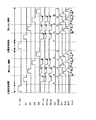
(First embodiment)
First, a first embodiment of the present invention will be described. FIG. 1 is a diagram showing a two-dimensional circuit configuration of an X-ray imaging apparatus (radiation imaging apparatus) according to the first embodiment of the present invention. However, FIG. 1
図1において、S(1−1)〜S(3−3)は、X線を波長変換体により変換された可視光を電気信号に変換する光電変換素子であり、本実施形態ではPIN型光電変換素子である。PIN型光電変換素子は、回路記号上ダイオードで示している。T1(1−1)〜T1(3−3)は、光電変換素子のアノード側(P側)の電極がゲート端子に接続された第1のTFTである。T2(1−1)〜T2(3−3)は、走査において光電変換素子の電気信号を行単位に選択的に読み出しするために設けられた第2のTFTである。T3(1−1)〜T3(3−3)は、電気信号を読み出された光電変換素子をリセットするために設けられた第3のTFTである。 In FIG. 1, S (1-1) to S (3-3) are photoelectric conversion elements that convert visible light obtained by converting X-rays by a wavelength converter into an electrical signal. It is a conversion element. The PIN type photoelectric conversion element is indicated by a diode on a circuit symbol. T1 (1-1) to T1 (3-3) are first TFTs in which the anode side (P side) electrode of the photoelectric conversion element is connected to the gate terminal. T2 (1-1) to T2 (3-3) are second TFTs provided for selectively reading out the electric signal of the photoelectric conversion element in units of rows in scanning. T3 (1-1) to T3 (3-3) are third TFTs provided to reset the photoelectric conversion element from which the electric signal is read.
G1〜G4は、第2のTFTであるT2(1−1)〜T2(3−3)及び第3のTFTであるT3(1−1)〜T3(3−3)をオン/オフさせるためのゲート配線であり、M1〜M3は信号配線である。Vs共通配線は、光電変換素子S(1−1)〜S(3−3)のカソード(N側)の電極に正のバイアスを与えるための全画素に共通の配線である。また、Vr共通配線は、光電変換素子S(1−1)〜S(3−3)のアノード電極にリセットバイアスを与えるための全画素に共通の配線である。 G1 to G4 turn on / off the second TFTs T2 (1-1) to T2 (3-3) and the third TFTs T3 (1-1) to T3 (3-3). The gate wirings M1 to M3 are signal wirings. The Vs common wiring is a wiring common to all the pixels for applying a positive bias to the cathode (N side) electrodes of the photoelectric conversion elements S (1-1) to S (3-3). The Vr common wiring is a wiring common to all pixels for applying a reset bias to the anode electrodes of the photoelectric conversion elements S (1-1) to S (3-3).
本実施形態では、光電変換素子S(1−1)〜S(3−3)、第1のTFT(T1(1−1)〜T1(3−3))、第2のTFT(T2(1−1)〜T2(3−3))、第3のTFT(T3(1−1)〜T3(3−3))、ゲート配線G1〜G3、信号配線M1〜M3、Vs共通配線及びVr共通配線が光電変換回路部(放射線検出回路部)1に含まれている。 In the present embodiment, the photoelectric conversion elements S (1-1) to S (3-3), the first TFT (T1 (1-1) to T1 (3-3)), and the second TFT (T2 (1) -1) to T2 (3-3)), the third TFT (T3 (1-1) to T3 (3-3)), gate wirings G1 to G3, signal wirings M1 to M3, Vs common wiring and Vr common A wiring is included in the photoelectric conversion circuit unit (radiation detection circuit unit) 1.
また、シフトレジスタSR1は、ゲート配線G1〜G4に駆動用のパルス電圧を与え、光電変換素子S(1−1)〜S(3−3)の電気信号を行単位で第1のTFT(T1(1−1)〜T1(3−3))から読み出すために、第2のTFT(T2(1−1)〜T2(3−3))及び第3のTFT(T3(1−1)〜T3(3−3))をオン/オフさせる駆動用回路部である。 Further, the shift register SR1 applies a driving pulse voltage to the gate wirings G1 to G4, and the electric signals of the photoelectric conversion elements S (1-1) to S (3-3) are supplied to the first TFT (T1) in units of rows. In order to read from (1-1) to T1 (3-3)), the second TFT (T2 (1-1) to T2 (3-3)) and the third TFT (T3 (1-1) to This is a driving circuit section for turning on / off T3 (3-3).
読み出し用回路部2は、光電変換回路部1からの並列の出力信号を読み取り、直列変換して出力する。A1〜A3は、信号配線M1〜M3に反転端子(−)が接続されたオペアンプである。この反転端子(−)と出力端子の間には、夫々容量素子Cf1〜Cf3が接続されている。また、信号配線M1〜M3には、夫々電流源I1〜I3が接続されている。容量素子Cf1〜Cf3は、第2のTFT(T2(1−1)〜T2(3−3))がオンしたときに、光電変換素子S(1−1)〜S(3−3)の電気信号を蓄積する。RES1〜RES3は、容量素子Cf1〜Cf3をリセットするスイッチであり、容量素子Cf1〜Cf3と並列に接続されている。図1では、リセットバイアスは、GNDで表記している。CL1〜CL3は、容量素子Cf1〜Cf3に蓄積された信号を一時的に記憶するサンプルホールド容量である。また、Sn1〜Sn3は、サンプルホールド容量CL1〜CL3でサンプルホールドを行うためのスイッチ、B1〜B3はバッファアンプ、Sr1〜Sr3は、並列信号を直列変換するためのスイッチ、SR2はSr1〜Sr3に直列変換するためのパルスを与えるシフトレジスタ、1000は直列変換された信号を出力するアンプである。
The reading circuit unit 2 reads parallel output signals from the photoelectric
読み出し用回路部2には、更に、光電変換回路部1内のVs共通配線を介し光電変換素子の電極にバイアスを与えるためのバイアス電源3、及び光電変換回路部1内のVr共通配線を介し光電変換素子の他方の電極にリセットバイアスを与えるためのリセット電源4が形成されている。
The readout circuit unit 2 further includes a
バイアス電源3には、バイアス電圧を出力するためのオペアンプAbが設けられ、リセット電源4には、リセット電圧を出力するためのオペアンプArが設けられている。図1において、バイアス電源3又はリセット電源4の点線部内に記載した直流電源は一定電位を与える規準電源であり、例えば、バンドギャップ法により作成された電源である。オペアンプAb及びArはバッファとして記載されているが、必要に応じて倍率を与えてもよい。また、バイアス電源3及びリセット電源4内の抵抗及びコンデンサは、電源の高周波数領域のノイズ成分を遮断するためのローパスフィルタを構成する。遮断周波数をできるだけ小さくするためには、コンデンサの容量を大きくすればよい。容量を読み出し用回路部2内に形成できない場合には、容量を外部に実装してもよい。
The
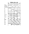
次に、上述のように構成された第1の実施形態の動作について説明する。図2は、本発明の第1の実施形態に係るX線撮像装置の動作を示すタイムチャートであり、2フレーム分の動作を表している。図2のタイムチャートには、光電変換期間及び読み出し期間の2つの動作期間を示してある。 Next, a description will be given of the operation of the first embodiment constructed as described above. FIG. 2 is a time chart showing the operation of the X-ray imaging apparatus according to the first embodiment of the present invention, and shows the operation for two frames. In the time chart of FIG. 2, two operation periods, a photoelectric conversion period and a readout period, are shown.
先ず、光電変換期間について説明する。全光電変換素子S(1−1)〜S(3−3)のカソード側電極(N電極)は、バイアス電源によりに正電位にバイアスされた状態にある。シフトレジスタSR1の信号はすべて“Lo”であり、第2のTFTであるT2(1−1)〜T2(3−3)及び第3のTFTであるT3(1−1)〜T3(3−3)はオフとなっている。この状態でX線がパルス的に入射すると、蛍光体(図1には図示せず)を介して各光電変換素子に可視光が照射され、PIN型光電変換素子のI層内で電子及びホールのキャリアが生成される。このとき、電子はセンサバイアスVsによりカソード側電極(N電極)、即ちバイアス電源側に移動する。一方、ホールは反対方向の第1のTFT側に移動し、主に光電変換素子内の容量に蓄えられる。この電荷は、X線の照射を停止した後においても保持される。 First, the photoelectric conversion period will be described. The cathode side electrodes (N electrodes) of all the photoelectric conversion elements S (1-1) to S (3-3) are biased to a positive potential by a bias power source. All signals of the shift register SR1 are “Lo”, and the second TFTs T2 (1-1) to T2 (3-3) and the third TFTs T3 (1-1) to T3 (3- 3) is off. When X-rays are incident in this state in a pulsed manner, visible light is irradiated to each photoelectric conversion element via a phosphor (not shown in FIG. 1), and electrons and holes are generated in the I layer of the PIN photoelectric conversion element. The carrier is generated. At this time, the electrons move to the cathode side electrode (N electrode), that is, the bias power source side by the sensor bias Vs. On the other hand, the hole moves to the first TFT side in the opposite direction and is mainly stored in the capacitor in the photoelectric conversion element. This charge is retained even after the X-ray irradiation is stopped.
次に、読み出し期間について説明する。読み出し動作は、第1行目の光電変換素子(S1−1〜S1−3)、続いて、第2行目の光電変換素子(S2−1〜S2−3)、続いて、第3行目の光電変換素子(S3−1〜S3−3)の順で行われる。 Next, the reading period will be described. The read operation is performed by the photoelectric conversion elements (S1-1 to S1-3) in the first row, the photoelectric conversion elements (S2-1 to S2-3) in the second row, and then the third row. The photoelectric conversion elements (S3-1 to S3-3) are performed in this order.
先ず、第1行目の光電変換素子(S1−1〜S1−3)を読み出すために、シフトレジスタSR1からゲート配線G1にゲートパルスを与え、第1行目の第2のTFT(T2(1−1)〜T2(1−3))をオンさせる。これにより、第1行目の光電変換素子(S1−1〜S1−3)の信号電荷に応じた電位がゲート端子に印加された第1行目の第1のTFT(T1(1−1)〜T1(1−3))にドレイン電流が流れ、読み出し用回路部2の初段部のオペアンプA1〜A3に接続されている容量素子Cf1〜Cf3に当該電流が流入して積分される。 First, in order to read out the photoelectric conversion elements (S1-1 to S1-3) in the first row, a gate pulse is given from the shift register SR1 to the gate wiring G1, and the second TFT (T2 (1 -1) to T2 (1-3)) are turned on. Accordingly, the first TFT (T1 (1-1)) in the first row in which the potential corresponding to the signal charge of the photoelectric conversion elements (S1-1 to S1-3) in the first row is applied to the gate terminal. To T1 (1-3)), the drain current flows, and the current flows into the capacitive elements Cf1 to Cf3 connected to the operational amplifiers A1 to A3 in the first stage of the readout circuit unit 2 and is integrated.
オペアンプA1〜A3の出力端子の電位は、光電変換素子の信号量に応じて、図2に示すように、負側へ変化する。第1行目の第2のTFT(T2(1−1)〜T2(1−3))が同時にオンするため、オペアンプA1〜A3の出力は同時に変化する。即ち、並列出力である。その状態で、SMPL信号をオンさせることにより、オペアンプA1〜A3の出力信号はサンプルホールド容量CL1〜CL3に転送され、SMPL信号をオフすると、一旦ホールドされる。続いて、シフトレジスタSR2からスイッチSr1、Sr2、Sr3の順番でパルスを印加すると、CL1、CL2、CL3の順で、ホールドされていた信号がアンプ1000を介して出力される。この結果、第1行目の光電変換素子(S1−1〜S1−3)の光電変換信号が順次、直列変換されて出力される。第2行目の光電変換素子(S2−1〜S2−3)の読み出し動作、第3行目の光電変換素子(S3−1〜S3−3)の読み出し動作も同様に行われる。
The potentials of the output terminals of the operational amplifiers A1 to A3 change to the negative side as shown in FIG. 2 according to the signal amount of the photoelectric conversion element. Since the second TFTs (T2 (1-1) to T2 (1-3)) in the first row are turned on at the same time, the outputs of the operational amplifiers A1 to A3 change simultaneously. That is, parallel output. In this state, when the SMPL signal is turned on, the output signals of the operational amplifiers A1 to A3 are transferred to the sample and hold capacitors CL1 to CL3. When the SMPL signal is turned off, the output signals are temporarily held. Subsequently, when pulses are applied from the shift register SR2 in the order of the switches Sr1, Sr2, and Sr3, the held signals are output via the
第1行目の読み出しにおいて、SMPL信号の変化によりオペアンプA1〜A3の信号をサンプルホールド容量CL1〜CL3にサンプルホールドすれば、第1行目の光電変換素子(S1−1〜S1−3)の信号は光電変換回路部1から出力されたことになる。従って、読み出し用回路部2内でスイッチSr1〜Sr3により直列変換されて出力されている最中に、光電変換回路部1内の第1行目の光電変換素子(S1−1〜S1−3)のリセット動作及び容量素子Cf1〜Cf3のリセット動作を行うことができる。
If the signals of the operational amplifiers A1 to A3 are sampled and held in the sample and hold capacitors CL1 to CL3 by the change of the SMPL signal in the reading of the first row, the photoelectric conversion elements (S1-1 to S1-3) of the first row The signal is output from the photoelectric
そこで、本実施形態では、第1行目の光電変換素子(S1−1〜S1−3)のリセット動作は、第2行目の光電変換素子(S2−1〜S2−3)の読み出し動作と同時に行う。これを実現するために、第1行目の第3のTFT(T3(1−1)〜T3(1−3))を制御するゲート配線と、第2行目の第2のTFT(T2(2−1)〜T2(2−3))を制御するゲート配線とを同じゲート配線G2で共有としている。即ち、本実施形態では、第n行目の光電変換素子の読み出し動作と、第(n−1)行目の光電変換素子のリセット動作とを同時に行う。 Therefore, in the present embodiment, the reset operation of the first row photoelectric conversion elements (S1-1 to S1-3) is the same as the read operation of the second row photoelectric conversion elements (S2-1 to S2-3). Do it at the same time. In order to realize this, the gate wiring for controlling the third TFTs (T3 (1-1) to T3 (1-3)) in the first row and the second TFT (T2 (T2 ( The same gate wiring G2 shares the gate wiring that controls (2-1) to T2 (2-3)). That is, in the present embodiment, the readout operation of the nth row photoelectric conversion element and the reset operation of the (n−1) th row photoelectric conversion element are performed simultaneously.
そして、このような光電変換期間と読み出し期間とを繰り返すことにより、連続した動画像を取得することができる。 A continuous moving image can be acquired by repeating the photoelectric conversion period and the readout period.
このような第1の実施形態によれば、バイアス電源3及びリセット電源4を、読み出し用回路部2内に配置しているため、Vs共通配線及びVr共通配線を、信号配線と同様に短くすることができる。従って、空間を介して飛び込んでくる外来ノイズを小さく抑えることができる。外来ノイズとは、主に、空間を介して飛び込んでくるノイズである。例えば、X線を発生させるX線源は、高圧電源を用いるがその高圧電源からのノイズや、自動車のイグニッションコイルからのノイズ、または他の電波機器からのノイズ、落雷によるノイズもこれに該当する。
According to the first embodiment, since the
一般に、第2のTFTがシフトレジスタ(SR1)により行単位でオン/オフする時等のVs共通配線に何らかの要因でノイズが加わっている時や、SMPL信号により読み出し用回路部内で行単位の信号がCl1〜CL3に転送する時のような光電変換素子の読み出し動作が行われている時に、出力信号にノイズが混入しやすい。これらは、画像上で、横スジ状の模様となり、画像品位を著しく劣化させる。これらの横スジ状のノイズは横ラインノイズ又は単にラインノイズとよばれる。また、第3のTFTがシフトレジスタ(SR1)により行単位でリセットが行われる時等のVr共通配線に何らかの要因でノイズが加わっている時にも、出力信号にノイズが混入しやすい。この場合にも、横ラインノイズが発生する。 In general, when noise is added to the Vs common wiring for some reason, such as when the second TFT is turned on / off in units of rows by the shift register (SR1), or in the readout circuit unit by the SMPL signal When the read operation of the photoelectric conversion element is performed as when the signal is transferred to Cl1 to CL3, noise is likely to be mixed into the output signal. These become a horizontal streak-like pattern on the image, and the image quality is remarkably deteriorated. These horizontal stripe noises are called horizontal line noise or simply line noise. Further, when noise is added to the Vr common wiring for some reason, such as when the third TFT is reset in units of rows by the shift register (SR1), noise is likely to be mixed into the output signal. Also in this case, horizontal line noise occurs.
従来、読み出し用回路部は、光電変換回路部の近傍に実装されている。その理由は、光電変換素子の信号は信号配線を介して読み出し用回路部内に転送されるため、配線をできるだけ短くすることが外来ノイズの抑制に効果的だからである。 Conventionally, the readout circuit section is mounted in the vicinity of the photoelectric conversion circuit section. The reason is that the signal of the photoelectric conversion element is transferred into the reading circuit portion through the signal wiring, and therefore, it is effective to suppress the external noise by making the wiring as short as possible.
そして、本実施形態では、バイアス電源3及びリセット電源4を構成するオペアンプAb及びArを読み出し用回路部2内に配置しているため、Vs共通配線及びVr共通配線を短くできるだけでなく、出力インピーダンスを低くすることができる。従って、外来ノイズが非常に混入しにくくなる。
In the present embodiment, since the operational amplifiers Ab and Ar constituting the
また、オペアンプAb及びArを読み出し用回路部2内に配置しているため、それら自身を低ノイズなものに設計することも可能である。つまり、オペアンプそのものがもつ有限のノイズ、即ちオペアンプを構成する個々の部品のジョンソンノイズ及びショットノイズのようなホワイトノイズ並びにフリッカノイズ(f分の1ノイズ)等に関して設計段階において最適化を図ることが可能である。 In addition, since the operational amplifiers Ab and Ar are arranged in the readout circuit unit 2, they can be designed to have low noise. In other words, it is possible to optimize the finite noise of the operational amplifier itself, that is, white noise such as Johnson noise and shot noise of individual components constituting the operational amplifier and flicker noise (1 / f noise) at the design stage. Is possible.
なお、一般に、読み出し用回路部としては、シリコンを主たる材料にした集積回路(IC)が用いられている。例えば、MOSトランジスタやバイポーラトランジスタを用いて、オペアンプやアナログスイッチ素子などを設計し、読み出し用回路部をICチップとして作製することができる。バイアス電源3及びリセット電源4も、同様の設計技法を用いれば、図1に示すように読み出し用回路部2内に作製することが可能である。
In general, an integrated circuit (IC) using silicon as a main material is used as the reading circuit portion. For example, an operational amplifier, an analog switch element, or the like can be designed using a MOS transistor or a bipolar transistor, and the reading circuit portion can be manufactured as an IC chip. The
また、本実施形態では、バイアス電源3及びリセット電源4の双方を読み出し用回路部2内に形成しているが、いずれか一方のみを形成してもよい。
In the present embodiment, both the
更に、本実施形態では、X線をパルス状に照射した光電変換期間を設けているが、X線を常時照射させて読み出し期間だけを繰り返すことにより連続した動画像を取得することもできる。この場合、各行単位で光電変換素子の蓄積期間がずれていくために、画像を観察時に違和感になることがある。 Furthermore, in this embodiment, a photoelectric conversion period in which X-rays are irradiated in a pulse shape is provided, but continuous moving images can be acquired by always irradiating X-rays and repeating only the readout period. In this case, since the accumulation periods of the photoelectric conversion elements are shifted in units of rows, it may be uncomfortable when observing the image.
また、本実施形態では、PIN型光電変換素子のカソード側(P側)にVs共通配線を介してバイアス電源から正バイアスに与えているが、反対のアノード側(N側)をVs共通配線として、バイアス電源から負バイアスに与えてもよい。この場合、図2のタイミングチャートにおいて、A1−out、A2−out、A3−out及びVoutの極性が反対になる。 In this embodiment, a positive bias is applied from the bias power supply to the cathode side (P side) of the PIN photoelectric conversion element via the Vs common wiring, but the opposite anode side (N side) is used as the Vs common wiring. A negative bias may be applied from a bias power source. In this case, in the timing chart of FIG. 2, the polarities of A1-out, A2-out, A3-out, and Vout are opposite.
(第2の実施形態)
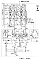
次に、本発明の第2の実施形態について説明する。図3は、本発明の第2の実施形態に係るX線撮像装置(放射線撮像装置)の2次元的な回路構成を示す図である。但し、図3には、説明を簡単化するために3×3=9画素分を記載している。
(Second Embodiment)
Next, a second embodiment of the present invention will be described. FIG. 3 is a diagram showing a two-dimensional circuit configuration of an X-ray imaging apparatus (radiation imaging apparatus) according to the second embodiment of the present invention. However, FIG. 3
図3において、S(1−1)〜S(3−3)は、X線を波長変換体により変換された可視光を電気信号に変換する光電変換素子であり、本実施形態ではMIS型光電変換素子である。T1(1−1)〜T1(3−3)は、光電変換素子のG電極がゲート端子に接続された第1のTFTである。T2(1−1)〜T2(3−3)は、走査において光電変換素子の電気信号を行単位に選択的に読み出しするために設けられた第2のTFTである。T3(1−1)〜T3(3−3)は、電気信号を読み出された光電変換素子をリフレッシュ又はリセットするために設けられた第3のTFTである。 In FIG. 3, S (1-1) to S (3-3) are photoelectric conversion elements that convert visible light obtained by converting X-rays by a wavelength converter into electrical signals. In this embodiment, MIS type photoelectric conversion is performed. It is a conversion element. T1 (1-1) to T1 (3-3) are first TFTs in which the G electrode of the photoelectric conversion element is connected to the gate terminal. T2 (1-1) to T2 (3-3) are second TFTs provided for selectively reading out the electric signal of the photoelectric conversion element in units of rows in scanning. T3 (1-1) to T3 (3-3) are third TFTs provided for refreshing or resetting the photoelectric conversion elements from which electric signals are read.
G1〜G4は、第2のTFTであるT2(1−1)〜T2(3−3)及び第3のTFTであるT3(1−1)〜T3(3−3)をオン/オフさせるためのゲート配線であり、M1〜M3は信号配線である。Vs共通配線は、光電変換素子S(1−1)〜S(3−3)のD電極にセンサバイアス(Vs)又は第2のリフレッシュバイアス(Vref2)を与えるための全画素に共通の配線である。また、Vr共通配線は、光電変換素子S(1−1)〜S(3−3)のG電極にリセットバイアス(Vrst)又は第1のリフレッシュバイアス(Vref1)を与えるための全画素に共通の配線である。 G1 to G4 turn on / off the second TFTs T2 (1-1) to T2 (3-3) and the third TFTs T3 (1-1) to T3 (3-3). The gate wirings M1 to M3 are signal wirings. The Vs common wiring is a wiring common to all the pixels for applying the sensor bias (Vs) or the second refresh bias (Vref2) to the D electrodes of the photoelectric conversion elements S (1-1) to S (3-3). is there. The Vr common wiring is common to all the pixels for applying the reset bias (Vrst) or the first refresh bias (Vref1) to the G electrodes of the photoelectric conversion elements S (1-1) to S (3-3). Wiring.
光電変換素子S(1−1)〜S(3−3)の黒く塗りつぶされた側の電極はG電極であり、対向側はD電極である。D電極は、Vs共通配線の一部と共有しているが、光を入射させる都合上、薄いN+層をD電極として利用している。本実施形態では、光電変換素子S(1−1)〜S(3−3)、第1のTFT(T1(1−1)〜T1(3−3))、第2のTFT(T2(1−1)〜T2(3−3))、第3のTFT(T3(1−1)〜T3(3−3))、ゲート配線G1〜G3、信号配線M1〜M3、Vs共通配線及びVr共通配線が光電変換回路部(放射線検出回路部)31に含まれている。 The electrodes on the sides of the photoelectric conversion elements S (1-1) to S (3-3) that are painted black are G electrodes, and the opposite side is a D electrode. The D electrode is shared with a part of the Vs common wiring, but a thin N + layer is used as the D electrode for the convenience of light incidence. In the present embodiment, the photoelectric conversion elements S (1-1) to S (3-3), the first TFT (T1 (1-1) to T1 (3-3)), and the second TFT (T2 (1) -1) to T2 (3-3)), the third TFT (T3 (1-1) to T3 (3-3)), gate wirings G1 to G3, signal wirings M1 to M3, Vs common wiring and Vr common The wiring is included in the photoelectric conversion circuit unit (radiation detection circuit unit) 31.
また、シフトレジスタSR1は、ゲート配線G1〜G4に駆動用のパルス電圧を与え、光電変換素子S(1−1)〜S(3−3)の電気信号を行単位で第1のTFT(T1(1−1)〜T1(3−3))から読み出すために、第2のTFT(T2(1−1)〜T2(3−3))や第3のTFT(T3(1−1)〜T3(3−3))をオン/オフさせる駆動用回路部である。 Further, the shift register SR1 applies a driving pulse voltage to the gate wirings G1 to G4, and the electric signals of the photoelectric conversion elements S (1-1) to S (3-3) are supplied to the first TFT (T1) in units of rows. In order to read from (1-1) to T1 (3-3)), the second TFT (T2 (1-1) to T2 (3-3)) and the third TFT (T3 (1-1) to This is a driving circuit section for turning on / off T3 (3-3).
読み出し用回路部32は、光電変換回路部31からの並列の出力信号を読み取り、直列変換して出力する。A1〜A3は、信号配線M1〜M3に反転端子(−)が接続されたオペアンプである。この反転端子(−)と出力端子の間には、夫々容量素子Cf1〜Cf3が接続されている。また、信号配線M1〜M3には、夫々電流源I1〜I3が接続されている。容量素子Cf1〜Cf3は、第2のTFT(T2(1−1)〜T2(3−3))がオンしたときに、光電変換素子S(1−1)〜S(3−3)の電気信号を蓄積する。RES1〜RES3は、容量素子Cf1〜Cf3をリセットするスイッチであり、容量素子Cf1〜Cf3と並列に接続されている。図3では、リセットバイアスは、GNDで表記している。CL1〜CL3は、容量素子Cf1〜Cf3に蓄積された信号を一時的に記憶するサンプルホールド容量である。また、Sn1〜Sn3は、サンプルホールド容量CL1〜CL3でサンプルホールドを行うためのスイッチ、B1〜B3はバッファアンプ、Sr1〜Sr3は、並列信号を直列変換するためのスイッチ、SR2はSr1〜Sr3に直列変換するためのパルスを与えるシフトレジスタ、1000は直列変換された信号を出力するアンプである。
The reading circuit unit 32 reads parallel output signals from the photoelectric conversion circuit unit 31, converts them in series, and outputs them. A1 to A3 are operational amplifiers in which inverting terminals (−) are connected to the signal wirings M1 to M3. Capacitance elements Cf1 to Cf3 are connected between the inverting terminal (−) and the output terminal, respectively. Further, current sources I1 to I3 are connected to the signal wirings M1 to M3, respectively. The capacitive elements Cf1 to Cf3 are electrically connected to the photoelectric conversion elements S (1-1) to S (3-3) when the second TFTs (T2 (1-1) to T2 (3-3)) are turned on. Accumulate the signal. RES1 to RES3 are switches that reset the capacitive elements Cf1 to Cf3, and are connected in parallel to the capacitive elements Cf1 to Cf3. In FIG. 3, the reset bias is expressed in GND. CL1 to CL3 are sample and hold capacitors that temporarily store signals accumulated in the capacitive elements Cf1 to Cf3. Sn1 to Sn3 are switches for performing sample and hold with the sample and hold capacitors CL1 to CL3, B1 to B3 are buffer amplifiers, Sr1 to Sr3 are switches for serially converting parallel signals, and SR2 is to Sr1 to Sr3. A
読み出し用回路部32には、更に、光電変換回路部31内のVs共通配線を介し光電変換素子のD電極にセンサバイアス(Vs)又はリフレッシュバイアス(Vref2)を与えるためのバイアス電源33、及び光電変換回路部1内のVr共通配線を介し光電変換素子の他方のG電極にリセットバイアス(Vrst)又はリフレッシュバイアス(Vref1)を与えるためのリセット電源34が形成されている。
The readout circuit unit 32 further includes a bias power supply 33 for applying a sensor bias (Vs) or a refresh bias (Vref2) to the D electrode of the photoelectric conversion element via the Vs common wiring in the photoelectric conversion circuit unit 31, and a photoelectric A reset power supply 34 for applying a reset bias (Vrst) or a refresh bias (Vref1) to the other G electrode of the photoelectric conversion element is formed through a Vr common line in the
バイアス電源33は、光電変換回路部31内のVs共通配線を介し光電変換素子のD電極に供給するバイアスを、Vs/XVref2制御信号でセンサバイアス(Vs)又はリフレッシュバイアス(Vref2)に切り替えることができるように構成されている。Vs/XVref2制御信号が“Hi”の時にはVsを供給し、“Lo”の時にはVref2を供給する。なお、本実施形態では、Vs>Vref2の関係がある。 The bias power supply 33 can switch the bias supplied to the D electrode of the photoelectric conversion element via the Vs common line in the photoelectric conversion circuit unit 31 to the sensor bias (Vs) or the refresh bias (Vref2) by the Vs / XVref2 control signal. It is configured to be able to. When the Vs / XVref2 control signal is “Hi”, Vs is supplied, and when it is “Lo”, Vref2 is supplied. In the present embodiment, there is a relationship of Vs> Vref2.
また、リセット電源34は、光電変換回路部31内のVr共通配線を介し光電変換素子のG電極に供給するバイアスを、Vref1/XVrst制御信号でリセットバイアス(Vrst)又はリフレッシュバイアス(Vref1)に切り替えることができるように構成されている。Vref1/XVrst制御信号が“Hi”の時にはVref1を供給し、“Lo”の時にはVrstを供給する。なお、本実施形態では、Vref1>Vrstの関係がある。 The reset power supply 34 switches the bias supplied to the G electrode of the photoelectric conversion element via the Vr common wiring in the photoelectric conversion circuit unit 31 to the reset bias (Vrst) or the refresh bias (Vref1) by the Vref1 / XVrst control signal. It is configured to be able to. When the Vref1 / XVrst control signal is “Hi”, Vref1 is supplied, and when it is “Lo”, Vrst is supplied. In the present embodiment, there is a relationship of Vref1> Vrst.
なお、本実施形態では、MIS型光電変換素子のリフレッシュ動作を、Vs共通配線を介して一括に行う方式とVr共通配線を介し行単位で行う方式とを選択できる。例えば、前者を静止画撮影モードとして、後者を動画撮影モードとして使用する放射線撮像装置ができる。 In this embodiment, it is possible to select a method in which the refresh operation of the MIS photoelectric conversion element is performed in a batch via the Vs common wiring and a method in which the refresh operation is performed in units of rows via the Vr common wiring. For example, a radiation imaging apparatus that uses the former as a still image shooting mode and the latter as a moving image shooting mode can be provided.
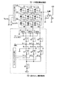
次に、上述のように構成された第2の実施形態の動作について説明する。図4は、本発明の第2の実施形態に係るX線撮像装置の動作を示すタイムチャートであり、2フレーム分の動作を表している。図4のタイムチャートには、光電変換期間及び読み出し期間の2つの動作期間を示してある。 Next, a description will be given of the operation of the second embodiment constructed as described above. FIG. 4 is a time chart showing the operation of the X-ray imaging apparatus according to the second embodiment of the present invention, and represents the operation for two frames. The time chart of FIG. 4 shows two operation periods, a photoelectric conversion period and a readout period.
先ず、光電変換期間について説明する。全光電変換素子S(1−1)〜S(3−3)のD電極は、読み取り用電源Vs(正電位)にバイアスされた状態にある。シフトレジスタSR1の信号はすべて“Lo”であり、第2のTFTであるT2(1−1)〜T2(3−3)及び第3のTFTであるT3(1−1)〜T3(3−3)はオフとなっている。この状態でX線がパルス的に入射すると、蛍光体を介して各光電変換素子のD電極(N+電極)に可視光が照射され、各光電変換素子のi層内で電子とホールのキャリアが生成される。このとき、電子はセンサバイアスVsによりD電極に移動するが、ホールは光電変換素子内のi層と絶縁層の界面に蓄えられ、X線の照射を停止した後においても保持される。 First, the photoelectric conversion period will be described. The D electrodes of all the photoelectric conversion elements S (1-1) to S (3-3) are biased to the reading power source Vs (positive potential). All signals of the shift register SR1 are “Lo”, and the second TFTs T2 (1-1) to T2 (3-3) and the third TFTs T3 (1-1) to T3 (3- 3) is off. When X-rays are incident in this state in a pulsed manner, visible light is irradiated to the D electrode (N + electrode) of each photoelectric conversion element via the phosphor, and carriers of electrons and holes in the i layer of each photoelectric conversion element. Is generated. At this time, electrons move to the D electrode by the sensor bias Vs, but holes are stored at the interface between the i layer and the insulating layer in the photoelectric conversion element, and are retained even after the X-ray irradiation is stopped.
次に、読み出し期間について説明する。読み出し動作は、第1行目の光電変換素子(S1−1〜S1−3)、続いて、第2行目の光電変換素子(S2−1〜S2−3)、続いて、第3行目の光電変換素子(S3−1〜S3−3)の順で行われる。 Next, the reading period will be described. The read operation is performed by the photoelectric conversion elements (S1-1 to S1-3) in the first row, the photoelectric conversion elements (S2-1 to S2-3) in the second row, and then the third row. The photoelectric conversion elements (S3-1 to S3-3) are performed in this order.
先ず、第1行目の光電変換素子(S1−1〜S1−3)を読み出すために、シフトレジスタSR1からゲート配線G1にゲートパルスを与え、第1行目の第2のTFT(T2(1−1)〜T2(1−3))をオンさせる。これにより、第1行目の光電変換素子(S1−1〜S1−3)の信号電荷に応じた電位がゲート端子に印加された第1行目の第1のTFT(T1(1−1)〜T1(1−3))にドレイン電流が流れ、読み出し用回路部2の初段部のオペアンプA1〜A3に接続されている容量素子Cf1〜Cf3に当該電流が流入して積分される。 First, in order to read out the photoelectric conversion elements (S1-1 to S1-3) in the first row, a gate pulse is given from the shift register SR1 to the gate wiring G1, and the second TFT (T2 (1 -1) to T2 (1-3)) are turned on. Accordingly, the first TFT (T1 (1-1)) in the first row in which the potential corresponding to the signal charge of the photoelectric conversion elements (S1-1 to S1-3) in the first row is applied to the gate terminal. To T1 (1-3)), the drain current flows, and the current flows into the capacitive elements Cf1 to Cf3 connected to the operational amplifiers A1 to A3 in the first stage of the readout circuit unit 2 and is integrated.
オペアンプA1〜A3の出力端子の電位は、光電変換素子の信号量に応じて、図4に示すように、負側に変化する。第1行目の第2のTFT(T2(1−1)〜T2(1−3))が同時にオンするため、オペアンプA1〜A3の出力は同時に変化する。即ち、並列出力である。その状態で、SMPL信号をオンさせることにより、オペアンプA1〜A3の出力信号はサンプルホールド容量CL1〜CL3に転送され、SMPL信号をオフすると、一旦ホールドされる。続いて、シフトレジスタSR2からスイッチSr1、Sr2、Sr3の順番でパルスを印加すると、CL1、CL2、CL3の順で、ホールドされていた信号がアンプ1000を介して出力される。この結果、第1行目の光電変換素子(S1−1〜S1−3)の光電変換信号が順次、直列変換されて出力される。第2行目の光電変換素子(S2−1〜S2−3)の読み出し動作、第3行目の光電変換素子(S3−1〜S3−3)の読み出し動作も同様に行われる。
The potentials of the output terminals of the operational amplifiers A1 to A3 change to the negative side as shown in FIG. 4 according to the signal amount of the photoelectric conversion element. Since the second TFTs (T2 (1-1) to T2 (1-3)) in the first row are turned on at the same time, the outputs of the operational amplifiers A1 to A3 change simultaneously. That is, parallel output. In this state, when the SMPL signal is turned on, the output signals of the operational amplifiers A1 to A3 are transferred to the sample and hold capacitors CL1 to CL3. When the SMPL signal is turned off, the output signals are temporarily held. Subsequently, when pulses are applied from the shift register SR2 in the order of the switches Sr1, Sr2, and Sr3, the held signals are output via the
第1行目の読み出しにおいて、SMPL信号の変化によりオペアンプA1〜A3の信号をサンプルホールド容量CL1〜CL3にサンプルホールドすれば、第1行目の光電変換素子(S1−1〜S1−3)の信号は光電変換回路部31から出力されたことになる。従って、読み出し用回路部32内でスイッチSr1〜Sr3により直列変換されて出力されている最中に、光電変換回路部31内の第1行目の光電変換素子(S1−1〜S1−3)のリフレッシュ動作及びリセット動作並びに容量素子Cf1〜Cf3のリセット動作を行うことができる。 If the signals of the operational amplifiers A1 to A3 are sampled and held in the sample and hold capacitors CL1 to CL3 by the change of the SMPL signal in the reading of the first row, the photoelectric conversion elements (S1-1 to S1-3) of the first row The signal is output from the photoelectric conversion circuit unit 31. Accordingly, the photoelectric conversion elements (S1-1 to S1-3) in the first row in the photoelectric conversion circuit unit 31 are being output while being serially converted by the switches Sr1 to Sr3 in the readout circuit unit 32. The refresh operation and the reset operation of the capacitor elements Cf1 to Cf3 can be performed.
そこで、本実施形態では、第1行目の光電変換素子(S1−1〜S1−3)のリフレッシュ動作は、第2行目の光電変換素子(S2−1〜S2−3)の読み出し動作と同時に行う。これを実現するために、第1行目の第3のTFT(T3(1−1)〜T3(1−3))を制御するゲート配線と、第2行目の第2のTFT(T2(2−1)〜T2(2−3))を制御するゲート配線は同じゲート配線G2で共有としている。 Therefore, in the present embodiment, the refresh operation of the photoelectric conversion elements (S1-1 to S1-3) in the first row is the same as the read operation of the photoelectric conversion elements (S2-1 to S2-3) in the second row. Do it at the same time. In order to realize this, the gate wiring for controlling the third TFTs (T3 (1-1) to T3 (1-3)) in the first row and the second TFT (T2 (T2 ( The gate wiring for controlling (2-1) to T2 (2-3)) is shared by the same gate wiring G2.
ゲート配線G2がオンしている間に、Vref1/XVrst制御信号が“Hi”になることにより、Vr共通配線がVref1にバイアスされ、第1行目の光電変換素子(S1−1〜S1−3)がリフレッシュされる。その後、同様に、ゲート配線G2がオンしている間に、Vref1/XVrst制御信号が“Lo”になることにより、Vr共通配線がリセットバイアスVrstにバイアスされ、第1行目の光電変換素子(S1−1〜S1−3)のG電極がリセットバイアスVrstによりリセットされる。このゲート配線G2がオンしている間は、同時に、第2行目の第2のTFT(T2(2−1)〜T2(2−3))がオン状態になっており、第2行目の光電変換素子(S2−1〜S2−3)の信号電荷に応じた電位が読み出される。このように、本実施形態では、第n行目の光電変換素子の読み出し動作と、第(n−1)行目の光電変換素子のリフレッシュ動作及びリセット動作とを同時に行う。 While the gate line G2 is on, the Vref1 / XVrst control signal becomes “Hi”, whereby the Vr common line is biased to Vref1, and the photoelectric conversion elements (S1-1 to S1-3) in the first row are biased. ) Is refreshed. Thereafter, similarly, the Vref1 / XVrst control signal becomes “Lo” while the gate line G2 is turned on, whereby the Vr common line is biased to the reset bias Vrst, and the photoelectric conversion element (first row) The G electrodes of S1-1 to S1-3) are reset by the reset bias Vrst. While the gate wiring G2 is on, the second TFTs (T2 (2-1) to T2 (2-3)) in the second row are on at the same time, and the second row Potentials corresponding to the signal charges of the photoelectric conversion elements (S2-1 to S2-3) are read out. As described above, in this embodiment, the readout operation of the photoelectric conversion element in the nth row and the refresh operation and reset operation of the photoelectric conversion element in the (n−1) th row are performed simultaneously.
そして、以上の動作を行うことにより、第1行目から第3行目のすべての光電変換素子S(1−1)〜S(3−3)の信号電荷を出力することができる。即ち、このような光電変換期間と読み出し期間とを繰り返すことにより、連続した動画像を取得することができる。 And by performing the above operation | movement, the signal charge of all the photoelectric conversion elements S (1-1) -S (3-3) of the 1st line to the 3rd line can be output. That is, a continuous moving image can be acquired by repeating such a photoelectric conversion period and a reading period.
このような第2の実施形態によれば、第1の実施形態と同様に、バイアス電源33及びリセット電源34を読み出し回路部32内に配置しているため、Vs共通配線及びVr共通配線の配線を、信号配線と同様に短くすることができる。従って、空間を介して飛び込んでくる外来ノイズを小さく抑えることができる。また、第1の実施形態と同様に、出力インピーダンスを低くすることができ、外来ノイズが非常に混入しにくくなる。更に、第1の実施形態と同様に、オペアンプAb及びArを読み出し用回路部32内に配置しているため、それら自身を低ノイズなものに設計することも可能である。 According to the second embodiment, since the bias power supply 33 and the reset power supply 34 are arranged in the readout circuit unit 32 as in the first embodiment, the Vs common wiring and the Vr common wiring are arranged. Can be shortened similarly to the signal wiring. Accordingly, it is possible to reduce external noise that jumps in through the space. Further, similarly to the first embodiment, the output impedance can be lowered, and external noise is hardly mixed. Furthermore, since the operational amplifiers Ab and Ar are arranged in the readout circuit section 32 as in the first embodiment, it is possible to design them with low noise.
更に、本実施形態では、すべての光電変換素子を一括でリフレッシュせず、各行単位でリフレッシュを行うため、リフレッシュ時の暗電流成分によるGND電位及び電源電位等の変動を少なくでき、動画のフレーム周波数を大きくすることができる。光電変換素子のリフレッシュ動作を全光電変換素子に共通のVs共通配線を介して行うことにより動画画像を得る場合、1フレ−ムに1回のリフレッシュ期間を設けることが必須である。このことは、特に、動画像を取得する際、フレ−ム周波数が小さくなる、即ち動作スピ−ドが遅くなるという問題を生じる。特に人体胸部を撮影する医療用のX線撮像装置の場合、大多数の画素を一括でリフレッシュすることは、リフレッシュ時に流れる電流も大きくなり、そしてGNDや電源ラインの電圧変動を大きくなり、すぐに画像を読み取ることは安定せず、良好な画像を得られない。これに対し、本実施形態のように、Vr共通配線を介して第3のTFT(T3(1−1)〜T3(3−3))をオンさせることによりリフレッシュ動作を行う場合には、行単位でリフレッシュ動作を行うことができるため、1度にリフレッシュされる画素数が少なく、リフレッシュ時に流れる電流を小さく抑えることができる。 Furthermore, in this embodiment, since all the photoelectric conversion elements are not refreshed at once, and refresh is performed in units of rows, fluctuations in the GND potential and the power supply potential due to the dark current component at the time of refresh can be reduced, and the frame frequency of the moving image Can be increased. When a moving image is obtained by performing the refresh operation of the photoelectric conversion elements via the Vs common wiring common to all the photoelectric conversion elements, it is essential to provide one refresh period per frame. This causes a problem that the frame frequency becomes small, that is, the operation speed becomes slow, particularly when a moving image is acquired. In particular, in the case of medical X-ray imaging devices that image the human chest, refreshing the majority of pixels at once increases the current that flows during the refresh, and increases the voltage fluctuations in the GND and the power supply line. Reading an image is not stable and a good image cannot be obtained. On the other hand, when the refresh operation is performed by turning on the third TFTs (T3 (1-1) to T3 (3-3)) through the Vr common wiring as in the present embodiment, Since the refresh operation can be performed in units, the number of pixels that are refreshed at a time is small, and the current that flows during refresh can be kept small.
なお、本実施形態では、バイアス電源33及びリセット電源34の双方を読み出し用回路部32内に形成しているが、いずれか一方のみを形成してもよい。 In the present embodiment, both the bias power source 33 and the reset power source 34 are formed in the read circuit unit 32, but only one of them may be formed.
(第3の実施形態)
次に、本発明の第3の実施形態について説明する。第3の実施形態では、第2の実施形態に係るX線撮像装置を透視モード(動画モード)で動作させている状態から、撮影者の静止画の撮影要求により、撮影モード(静止画モード)へ遷移させる。図5は、本発明の第3の実施形態におけるX線撮像装置の撮影シーケンスを示す図である。また、図6は、透視モード(動画モード)でのX線撮像装置の動作を示すタイムチャートであり、図7は、撮影モード(静止画モード)でのX線撮像装置の動作を示すタイムチャートである。
(Third embodiment)
Next, a third embodiment of the present invention will be described. In the third embodiment, from the state in which the X-ray imaging apparatus according to the second embodiment is operated in the fluoroscopic mode (moving image mode), the photographing mode (still image mode) is requested by the photographer taking a still image. Transition to. FIG. 5 is a diagram showing an imaging sequence of the X-ray imaging apparatus according to the third embodiment of the present invention. 6 is a time chart showing the operation of the X-ray imaging apparatus in the fluoroscopic mode (moving image mode), and FIG. 7 is a time chart showing the operation of the X-ray imaging apparatus in the imaging mode (still image mode). It is.
透視モードでは、図6に示すタイミング動作を繰り返す。透視モードの期間では、撮影者は、静止画像を撮影のための被写体(患者)の位置及び角度を決めるために、患者の透視画像をモニタする。また、一般的に、この期間中のX線量は弱めに照射する。そして、被写体(患者)の位置及び角度が決まると、撮影者がX線撮像装置に、静止画像を撮影する意思信号として曝射要求信号(撮影要求)を発令する。X線撮像装置は、この曝射要求信号を受けると、その動作モードを透視モードから撮影モードに遷移する。撮影モードでは、図8に示すタイミング動作を行う。 In the fluoroscopic mode, the timing operation shown in FIG. 6 is repeated. In the period of the fluoroscopic mode, the photographer monitors the fluoroscopic image of the patient in order to determine the position and angle of the subject (patient) for photographing the still image. In general, the X-ray dose during this period is weakly irradiated. When the position and angle of the subject (patient) are determined, the photographer issues an exposure request signal (imaging request) to the X-ray imaging apparatus as an intention signal for capturing a still image. When receiving the exposure request signal, the X-ray imaging apparatus changes its operation mode from the fluoroscopic mode to the imaging mode. In the photographing mode, the timing operation shown in FIG. 8 is performed.
なお、透視モード及び撮影モードの組み合わせ(流れ)は、図5に示すような撮影モードが1回だけのものに限定されない。例えば、撮影する被写体の撮影構図に応じて、透視モード→撮影モード→透視モード→撮影モード・・・と複数回、繰り返してもよい。 Note that the combination (flow) of the fluoroscopic mode and the photographing mode is not limited to the one in which the photographing mode as shown in FIG. 5 is performed only once. For example, the fluoroscopic mode → the imaging mode → the fluoroscopy mode → the imaging mode... May be repeated a plurality of times according to the imaging composition of the subject to be imaged.
また、透視モード(動画モード)においてX線をパルス状ではなく連続して照射してもよい。X線を連続して照射した場合の透視モードでのX線撮像装置の動作を示すタイムチャートを図8に示す。 Moreover, you may irradiate X-ray continuously instead of a pulse form in fluoroscopic mode (moving image mode). FIG. 8 shows a time chart showing the operation of the X-ray imaging apparatus in the fluoroscopic mode when X-rays are continuously irradiated.
X線を連続して照射した場合には、読み出し期間と光電変換期間とを単一の期間(光電変換及び読み出し期間)とすることができるため、透視モードにおける動作周波数を大きくすることができるという利点がある。また、X線をパルス状に入射させないため、X線発生源に対する負荷を軽減できる利点もある。 When X-rays are continuously irradiated, the readout period and the photoelectric conversion period can be made a single period (photoelectric conversion and readout period), so that the operating frequency in the fluoroscopic mode can be increased. There are advantages. Further, since X-rays are not incident in a pulsed manner, there is an advantage that the load on the X-ray generation source can be reduced.
第2の実施形態に係るX線撮像装置を透視装置に応用した場合、透視モードにおいては第3のTFT(T3(1−1)〜T3(3−3))を介して第1のリフレッシュバイアス(Vref1)を与え、透視撮影によって被写体の位置及び角度等を決定し、静止画撮影モードに遷移した際には、Vs共通配線から第2のリフレッシュバイアス(Vref2)を与える。Vs共通配線からのリフレッシュは、全画素一括で行うため、リフレッシュ動作後のGND電位及び系の基準電位の変動が大きくなり、その電位変動を待たなければ読み出し動作を行えない。従って、必ずしも、動画撮影(透視)には適しているとはいえない。 When the X-ray imaging apparatus according to the second embodiment is applied to a fluoroscopic apparatus, the first refresh bias is applied via the third TFT (T3 (1-1) to T3 (3-3)) in the fluoroscopic mode. (Vref1) is applied, the position and angle of the subject are determined by fluoroscopic imaging, and the second refresh bias (Vref2) is applied from the Vs common wiring when transitioning to the still image shooting mode. Since refresh from the Vs common line is performed for all pixels at once, fluctuations in the GND potential and the system reference potential after the refresh operation increase, and the readout operation cannot be performed unless the potential fluctuations are awaited. Therefore, it is not necessarily suitable for moving image shooting (perspective).
しかし、この反面、バイアス電源33と光電変換素子S(1−1)〜S(3−3)との間に、従来の装置では必要とされているTFTが存在しないため、Vs共通配線と第2のリフレッシュバイアス(Vref2)の電位差を大きくすることが可能である。従って、飽和電荷を大きく設定できるという長所がある。つまり、診断画像を得るような静止画撮影には高いS/Nが求められ、第2のリフレッシュバイアス(Vref2)で共通配線Vs側からリフレッシュした方が好適である。 However, on the other hand, there is no TFT required in the conventional device between the bias power source 33 and the photoelectric conversion elements S (1-1) to S (3-3). The potential difference between the two refresh biases (Vref2) can be increased. Therefore, there is an advantage that the saturation charge can be set large. That is, a high S / N ratio is required for still image shooting for obtaining a diagnostic image, and it is preferable to refresh from the common wiring Vs side with the second refresh bias (Vref2).
(第4の実施形態)
次に、本発明の第4の実施形態について説明する。図9は、本発明の第4の実施形態に係るX線撮像装置(放射線撮像装置)の構造を示す模式図である。
(Fourth embodiment)
Next, a fourth embodiment of the present invention will be described. FIG. 9 is a schematic diagram showing a structure of an X-ray imaging apparatus (radiation imaging apparatus) according to the fourth embodiment of the present invention.
本実施形態では、読み出し用回路部及び駆動用回路部が、夫々複数ブロックに分割されて光電変換回路部に接続されている。図9内の黒い四角(■)は一画素を表しており、図内中央の円(○)内にその一画素分の回路を示している。本実施形態では、第2の実施形態と同様に、画素内に、MIS型光電変換素子、第1のTFT、第2のTFT及び第3のTFTが含まれているが、光電変換素子として、第1の実施形態と同様に、PIN型光電変換素子が用いられてもよい。
読み出し用回路部の各ブロックは、夫々AMP−IC1〜AMP−IC10と表示しており、駆動用回路部の各ブロックは、夫々DR−IC1〜DR−IC10と表示している。特に医療用X線撮像装置には、人体胸部の撮影に用いられるため、一般に、40cm×40cm以上の大面積撮影領域が要求されている。また、画素の解像度は100μm〜200μm程度必要といわれている。例えば、解像度が160μmで40cm×40cmの撮影領域をカバーするためには、2500画素×2500画素が必要となる。
In this embodiment, the reading circuit unit and the driving circuit unit are each divided into a plurality of blocks and connected to the photoelectric conversion circuit unit. A black square (■) in FIG. 9 represents one pixel, and a circuit for the one pixel is shown in a circle (◯) in the center of the figure. In the present embodiment, as in the second embodiment, the MIS type photoelectric conversion element, the first TFT, the second TFT, and the third TFT are included in the pixel. As the photoelectric conversion element, Similar to the first embodiment, a PIN photoelectric conversion element may be used.
Each block of the reading circuit portion is indicated as AMP-IC1 to AMP-IC10, and each block of the driving circuit portion is indicated as DR-IC1 to DR-IC10, respectively. In particular, since medical X-ray imaging apparatuses are used for imaging the human chest, a large area imaging area of 40 cm × 40 cm or more is generally required. It is said that the pixel resolution is required to be about 100 μm to 200 μm. For example, in order to cover a 40 cm × 40 cm imaging region with a resolution of 160 μm, 2500 pixels × 2500 pixels are required.
読み出し用回路部及び駆動用回路部は、一般にシリコンテクノロジーを用いて集積回路(IC)として製造される。シリコンウェハは、一般には、用途に応じて複数個のチップに切り出されて、ICとして製造される。本実施形態においては、一つの読み出し用回路部を256列の画素分を読み出しするブロックとしている。また一つの駆動用回路部は256行分の画素を駆動するブロックとしている。このように分配することにより、読み出し用回路部及び駆動用回路部は、夫々10ブロックに分割することができる。読み出し回路部における余りのチャネル、即ち(256×10)−2500=60チャネル分は、GND電位を入力するかオープンにしておく。第1の実施形態1及び第2の実施形態のようなN行目のリセットと(N+1)行目の読み出しとを同時に行う構成の場合、1チャネル多く使用するために、駆動用回路部における余りのチャネル数は、59チャネルとなり、このチャネルはオープンにしておく。 The reading circuit section and the driving circuit section are generally manufactured as an integrated circuit (IC) using silicon technology. In general, a silicon wafer is cut into a plurality of chips according to applications and manufactured as an IC. In the present embodiment, one readout circuit unit is a block that reads out 256 columns of pixels. One driving circuit unit is a block for driving pixels for 256 rows. By distributing in this way, the reading circuit unit and the driving circuit unit can be divided into 10 blocks. For the remaining channels in the readout circuit portion, that is, (256 × 10) −2500 = 60 channels, the GND potential is input or left open. In the case where the N-th row reset and the (N + 1) -th row readout are performed simultaneously as in the first embodiment and the second embodiment, the remainder in the drive circuit section is used in order to use more channels. The number of channels is 59, and these channels are left open.
また、本実施形態では、読み出し回路部の各ブロックに、Vs共通配線に電位を与えるためのバイアス電源とVr共通配線の電位を与えるリセット電源が接続されているが、いずれか一方のみが接続されていてもよい。図9に示す構成とすることにより、バイアス電源又はリセット電源が光電変換回路部の近傍に配置され、Vs共通配線及びVr共通配線のインピーダンスが低減し、S/Nが有利になる。 In this embodiment, a bias power supply for applying a potential to the Vs common wiring and a reset power supply for applying a potential of the Vr common wiring are connected to each block of the readout circuit unit, but only one of them is connected. It may be. With the configuration shown in FIG. 9, a bias power source or a reset power source is arranged in the vicinity of the photoelectric conversion circuit unit, the impedance of the Vs common wiring and the Vr common wiring is reduced, and S / N becomes advantageous.
バイアス電源は、光電変換素子がMIS型の場合、Vs共通配線を介してセンサの一方の電極にセンサバイアス(Vs)又は第2のリフレッシュバイアス(Vref2)を印加するためのものであるが、PIN型の場合は、センサバイアス(Vs)を印加するためのものである。また、リセット電源は、光電変換素子がMIS型の場合Vr、共通配線を介してセンサの反対側の電極にリセットバイアス(Vrst)又は第1のリフレッシュバイアス(Vref1)を印加するためのものであるが、PIN型の場合は、リセットバイアス(Vrst)を印加するためのものである。 The bias power supply is for applying the sensor bias (Vs) or the second refresh bias (Vref2) to one electrode of the sensor via the Vs common wiring when the photoelectric conversion element is the MIS type. In the case of the mold, the sensor bias (Vs) is applied. The reset power supply is for applying a reset bias (Vrst) or a first refresh bias (Vref1) to the opposite electrode of the sensor via Vr when the photoelectric conversion element is an MIS type. However, in the case of the PIN type, the reset bias (Vrst) is applied.
なお、本実施形態では読み出し回路部及び駆動用回路部の一つのブロックを256チャネルとしているが、チャネル数はこれに限るものではなく、製造時の簡便性及びウェハから切り出せる良品チップの歩留まり等に基づいて選択することができる。 In this embodiment, one block of the readout circuit portion and the drive circuit portion is 256 channels. However, the number of channels is not limited to this, and the simplicity of manufacturing and the yield of non-defective chips that can be cut from the wafer, etc. Can be selected based on
(第5の実施形態)
次に、本発明の第5の実施形態について説明する。第5の実施形態は、本発明に係るX線撮像装置(放射線撮像装置)をX線診断システムに応用したものである。図10は、本発明の第5の実施形態に係るX線診断システムを示す模式図である。
(Fifth embodiment)
Next, a fifth embodiment of the present invention will be described. In the fifth embodiment, the X-ray imaging apparatus (radiation imaging apparatus) according to the present invention is applied to an X-ray diagnostic system. FIG. 10 is a schematic diagram showing an X-ray diagnostic system according to the fifth embodiment of the present invention.
X線ルーム(撮影室)内において、X線チューブ(X線発生装置)6050で発生したX線6060は患者又は被験者6061の胸部6062を透過し、イメージセンサ6040に入射する。この入射したX線には患者6061の内部の情報が含まれている。X線の入射に対応してシンチレータ(蛍光体)は発光し、これをセンサーパネルの光電変換素子が光電変換して、電気的情報を得る。イメージセンサ6040は、この情報を電気信号(ディジタル信号)としてイメージプロセッサ6070に出力する。画像処理手段としてのイメージプロセッサ6070は、受信した信号に対して画像処理を施して、コントロールルーム(操作室)の表示手段であるディスプレイ6080に出力する。ユーザは、ディスプレイ6080に表示された画像を観察して、患者6061の内部の情報を得ることができる。なお、イメージプロセッサ6070は、制御手段の機能も有しており、動画/静止画の撮影モードを切り換えたり、X線チューブ6050の制御を行ったりすることも可能である。
In the X-ray room (imaging room), the
また、イメージプロセッサ6070は、イメージセンサ6040から出力された電気信号を電話回線6090等の伝送処理手段を介して遠隔地へ転送し、ドクタールーム等の別の場所にある表示手段(ディスプレイ)6081に表示することもできる。また、イメージセンサ6040から出力された電気信号を光ディスク等の記録手段に保存し、この記録手段を用いて遠隔地の医師が診断することも可能である。また、記録手段となるフィルムプロセッサ6100によりフィルム6110に記録することもできる。
Further, the
なお、光電変換素子の構造は特に限定されるものではない。例えば、アモルファスシリコンを主原料とし、放射線を可視光に変換する波長変換体からの可視光を吸収し電気信号に変換する光電変換素子が用いられてもよい。このような素子としては、例えば、アクセプタ不純物をドープしたP層と、真性半導体層であるI層と、ドナー不純物をドープしたN層と、を有するPIN型光電変換素子、及び、基板上に形成された金属薄膜層と、この金属薄膜層上に形成され、電子及び正孔の通過を阻止するアモルファス窒化シリコンからなる絶縁層と、この絶縁層上に形成された水素化アモルファスシリコンからなる光電変換層と、この光電変換層上に形成され、正孔の注入を阻止するN型の注入阻止層と、この注入阻止層上に形成された導電層と、を有するMIS型光電変換素子等が挙げられる。MIS型光電変換素子では、導電層は透明導電層であってもよく、また、導電層が注入阻止層上の一部に形成されていてもよい。これらの光電変換素子が用いられ、波長変換体が必要とされる場合、波長変換体としては、例えばGd2O2S、Gd2O3又はCsIを主成分とするものを用いることができる。更に、光電変換素子として、アモルファスセレン、ガリウム砒素、ヨウ化鉛又はヨウ化水銀を含有し、照射された放射線を吸収し直接電気信号に変換する素子を用いてもよい。 Note that the structure of the photoelectric conversion element is not particularly limited. For example, a photoelectric conversion element that uses amorphous silicon as a main raw material and absorbs visible light from a wavelength converter that converts radiation into visible light and converts it into an electrical signal may be used. As such an element, for example, a PIN photoelectric conversion element having a P layer doped with an acceptor impurity, an I layer that is an intrinsic semiconductor layer, and an N layer doped with a donor impurity, and formed on a substrate A metal thin film layer formed thereon, an insulating layer made of amorphous silicon nitride formed on the metal thin film layer to block passage of electrons and holes, and photoelectric conversion made of hydrogenated amorphous silicon formed on the insulating layer MIS type photoelectric conversion element having a layer, an N type injection blocking layer formed on the photoelectric conversion layer and blocking hole injection, and a conductive layer formed on the injection blocking layer. It is done. In the MIS photoelectric conversion element, the conductive layer may be a transparent conductive layer, or the conductive layer may be formed on a part of the injection blocking layer. When these photoelectric conversion elements are used and a wavelength converter is required, as the wavelength converter, for example, a substance mainly composed of Gd 2 O 2 S, Gd 2 O 3 or CsI can be used. Further, as the photoelectric conversion element, an element containing amorphous selenium, gallium arsenide, lead iodide or mercury iodide and absorbing irradiated radiation and directly converting it into an electrical signal may be used.
また、読み出し用回路部の構造も特に限定されるものではなく、例えば、光電変換回路部から読み出した信号を増幅する増幅手段と、この増幅手段により増幅された信号を蓄積する蓄積手段と、この蓄積手段により蓄積された信号をシリアル変換するシリアル変換手段と、を有するものを用いることができる。 Further, the structure of the readout circuit section is not particularly limited. For example, an amplification means for amplifying a signal read from the photoelectric conversion circuit section, an accumulation means for accumulating the signal amplified by the amplification means, and this It is possible to use one having serial conversion means for serially converting the signal stored by the storage means.
なお、本発明の実施形態は、例えばコンピュータがプログラムを実行することによって実現することができる。また、プログラムをコンピュータに供給するための手段、例えばかかるプログラムを記録したCD−ROM等のコンピュータ読み取り可能な記録媒体又はかかるプログラムを伝送するインターネット等の伝送媒体も本発明の実施形態として適用することができる。また、上記のプログラムも本発明の実施形態として適用することができる。上記のプログラム、記録媒体、伝送媒体及びプログラムプロダクトは、本発明の範疇に含まれる。 The embodiment of the present invention can be realized by, for example, a computer executing a program. Also, means for supplying a program to a computer, for example, a computer-readable recording medium such as a CD-ROM recording such a program, or a transmission medium such as the Internet for transmitting such a program is also applied as an embodiment of the present invention. Can do. The above program can also be applied as an embodiment of the present invention. The above program, recording medium, transmission medium, and program product are included in the scope of the present invention.
S(1−1)〜S(3−3):光電変換素子
T1(1−1)〜T1(3−3):第1のTFT(ソースフォロア接続)
T2(1−1)〜T2(3−3):第2のTFT(スイッチ機能)
T3(1−1)〜T3(3−3):第3のTFT(スイッチ機能)
SR1:シフトレジスタ
SR2:シフトレジスタ
A1〜A3:オペアンプ
B1〜B3:オペアンプ
Ab:オペアンプ
Ar:オペアンプ
1000:オペアンプ
Cf1〜Cf3:容量素子
CL1〜CL3:容量素子
RES1〜RES3:スイッチ
Sn1〜Sn3:転送スイッチ
Sr1〜Sr3:読み出し用スイッチ
I1〜I3:電流源
1:光電変換回路部(放射線検出回路部)
2:読み出し用回路部
G1〜G3:ゲート駆動配線
M1〜M3:マトリクス信号配線
Vref1:第1のリフレッシュバイアス
Vref2:第2のリフレッシュバイアス
Vs:光電変換素子のセンサバイアス
Vrst:リセットバイアス
6040:イメージセンサ
6050:X線チューブ
6060:X線
6061:被験者
6070:イメージプロセッサ
6080:ディスプレイ
6081:ディスプレイ
6100:フィルムプロセッサ
6110:フィルム
S (1-1) to S (3-3): photoelectric conversion element T1 (1-1) to T1 (3-3): first TFT (source follower connection)
T2 (1-1) to T2 (3-3): second TFT (switch function)
T3 (1-1) to T3 (3-3): third TFT (switch function)
SR1: Shift register SR2: Shift register A1 to A3: Operational amplifier B1 to B3: Operational amplifier Ab: Operational amplifier Ar: Operational amplifier 1000: Operational amplifier Cf1 to Cf3: Capacitance element CL1 to CL3: Capacitance element RES1 to RES3: Switch Sn1 to Sn3: Transfer switch Sr1 to Sr3: Read switches I1 to I3: Current source 1: Photoelectric conversion circuit unit (radiation detection circuit unit)
2: Read circuit section G1 to G3: Gate drive wiring M1 to M3: Matrix signal wiring Vref1: First refresh bias Vref2: Second refresh bias Vs: Sensor bias of photoelectric conversion element Vrst: Reset bias 6040: Image sensor 6050: X-ray tube 6060: X-ray 6061: Subject 6070: Image processor 6080: Display 6081: Display 6100: Film processor 6110: Film
Claims (10)
前記光電変換回路部を駆動させる駆動用回路部と、
前記光電変換回路部から信号を読み出す読み出し用回路部と、
を有し、
前記画素は、
第1及び第2の電極を有して入射した放射線を電気信号に変換する光電変換素子と、
前記第1の電極に接続されるゲート電極を有して前記光電変換素子が生成した電気信号を前記読み出し用回路部に出力するソースフォロア型の第1の電界効果トランジスタと、
前記駆動用回路部により行単位で選択された画素から電気信号を前記読み出し用回路部に出力する際に導通状態となる第2の電界効果トランジスタと、
前記駆動用回路部により行単位で選択された画素に設けられた光電変換素子をリセットする際に導通状態となる第3の電界効果トランジスタと、
を有し、
前記読み出し用回路部は集積回路が用いられて前記光電変換回路部の近傍に実装され、
前記光電変換素子に光電変換用バイアスを与えるために複数の前記画素の前記第2の電極に共通に接続されるバイアス電源及び前記光電変換素子にリセット用バイアスを与えるために複数の前記画素の前記第3の電界効果トランジスタに共通に接続されるリセット電源の少なくとも一方の電源が、前記読み出し用回路部の内部に配置されていることを特徴とする放射線撮像装置。 A photoelectric conversion circuit unit in which a plurality of pixels are arranged in an array on the substrate;
A driving circuit unit for driving the photoelectric conversion circuit unit;
A readout circuit unit for reading a signal from the photoelectric conversion circuit unit;
Have
The pixel is
A photoelectric conversion element having first and second electrodes for converting incident radiation into an electrical signal;
A source follower type first field effect transistor having a gate electrode connected to the first electrode and outputting an electric signal generated by the photoelectric conversion element to the readout circuit unit;
A second field effect transistor that becomes conductive when an electrical signal is output from the pixel selected in units of rows by the driving circuit unit to the reading circuit unit;
A third field effect transistor that becomes conductive when resetting a photoelectric conversion element provided in a pixel selected in units of rows by the drive circuit unit;
Have
The readout circuit unit is mounted in the vicinity of the photoelectric conversion circuit unit using an integrated circuit ,
A plurality of the pixels in order to provide a plurality of said second bias power supply and reset bias to the photoelectric conversion elements are connected in common to an electrode of the pixel to provide a photoelectric conversion bias to the photoelectric conversion element A radiation imaging apparatus, wherein at least one power source of a reset power source commonly connected to the third field effect transistor is arranged inside the readout circuit unit.
前記バイアス電源と前記リセット電源の少なくとも一方の電源が、複数のブロックに分割された前記読み出し用回路部の内部に配置されていることを特徴とする請求項1に記載の放射線撮像装置。 The readout circuit section is divided into a plurality of blocks,
The radiation imaging apparatus according to claim 1, wherein at least one of the bias power source and the reset power source is disposed inside the readout circuit unit divided into a plurality of blocks.
前記バイアス電源は、前記MIS型光電変換素子の前記第2の電極に与えるバイアスを、光電変換用バイアスと第1のリフレッシュ用バイアスとの間で切り替える第1のバイアス切り替え手段を有し、
前記リセット電源は、前記MIS型光電変換素子の前記第1の電極に与えるバイアスを、リセット用バイアスと第2のリフレッシュ用バイアスとの間で切り替える第2のバイアス切り替え手段を有することを特徴とする請求項1乃至3のいずれか1項に記載の放射線撮像装置。 The photoelectric conversion element is a MIS type photoelectric conversion element,
The bias power source includes first bias switching means for switching a bias to be applied to the second electrode of the MIS photoelectric conversion element between a photoelectric conversion bias and a first refresh bias,
The reset power supply includes a second bias switching unit that switches a bias applied to the first electrode of the MIS photoelectric conversion element between a reset bias and a second refresh bias. The radiation imaging apparatus according to claim 1.
前記第2のリフレッシュバイアスは、静止画画像を取得する際の前記MIS型変換素子のリフレッシュに用いられることを特徴とする請求項4に記載の放射線撮像装置。 The first refresh bias is used to refresh the MIS conversion element when acquiring a moving image.
The radiation imaging apparatus according to claim 4, wherein the second refresh bias is used for refreshing the MIS type conversion element when acquiring a still image.
前記基板上に形成された金属薄膜層と、
前記金属薄膜層上に形成され、電子及び正孔の通過を阻止するアモルファス窒化シリコンからなる絶縁層と、
前記絶縁層上に形成された水素化アモルファスシリコンからなる光電変換層と、
前記光電変換層上に形成され、正孔の注入を阻止するN型の注入阻止層と、
前記注入阻止層上に形成された導電層と、
を有し、
リフレッシュモードでは、前記MIS型光電変換素子に対して、正孔を前記光電変換層から前記導電層に導く方向に電界を与え、
光電変換モードでは、前記MIS型光電変換素子に対して、前記光電変換層に入射した放射線により発生した正孔を当該光電変換層に留まらせて電子を前記導電層に導く方向に電界を与え、
前記読み出し用回路部は、前記光電変換モードにおいて前記光電変換層に蓄積された正孔及び前記導電層に導かれた電子のいずれか一方の量を光信号として検出することを特徴とする請求項4又は5に記載の放射線撮像装置。 The MIS photoelectric conversion element is
A metal thin film layer formed on the substrate;
An insulating layer formed on the metal thin film layer and made of amorphous silicon nitride that blocks passage of electrons and holes; and
A photoelectric conversion layer made of hydrogenated amorphous silicon formed on the insulating layer;
An N-type injection blocking layer formed on the photoelectric conversion layer and blocking hole injection;
A conductive layer formed on the injection blocking layer;
Have
In the refresh mode, an electric field is applied to the MIS photoelectric conversion element in a direction in which holes are guided from the photoelectric conversion layer to the conductive layer,
In the photoelectric conversion mode, an electric field is applied to the MIS type photoelectric conversion element in a direction in which holes generated by radiation incident on the photoelectric conversion layer are retained in the photoelectric conversion layer and electrons are guided to the conductive layer.
The reading circuit unit detects an amount of one of holes accumulated in the photoelectric conversion layer and electrons guided to the conductive layer as an optical signal in the photoelectric conversion mode. The radiation imaging apparatus according to 4 or 5.
前記光電変換回路部からの出力信号を増幅する増幅手段と、
前記増幅手段によって増幅された出力信号を一時的に蓄積する蓄積手段と、
前記蓄積手段によって蓄積された出力信号をシリアル変換するシリアル変換手段と、
を有することを特徴する請求項1乃至6のいずれか1項に記載の放射線撮像装置。 The readout circuit unit includes:
Amplifying means for amplifying an output signal from the photoelectric conversion circuit section;
Storage means for temporarily storing the output signal amplified by the amplification means;
Serial conversion means for serially converting the output signal stored by the storage means;
The radiation imaging apparatus according to claim 1, comprising:
前記光電変換回路部に向けて被写体を介して放射線を発生させる放射線発生手段と、
を有することを特徴とする放射線撮像システム。 The radiation imaging apparatus according to any one of claims 1 to 9,
Radiation generating means for generating radiation through the subject toward the photoelectric conversion circuit unit;
A radiation imaging system comprising:
Priority Applications (3)
| Application Number | Priority Date | Filing Date | Title |
|---|---|---|---|
| JP2004148051A JP4307322B2 (en) | 2004-05-18 | 2004-05-18 | Radiation imaging apparatus and radiation imaging system |
| US11/127,077 US7514690B2 (en) | 2004-05-18 | 2005-05-12 | Radiation image pickup apparatus and its control method |
| US12/398,528 US7872218B2 (en) | 2004-05-18 | 2009-03-05 | Radiation image pickup apparatus and its control method |
Applications Claiming Priority (1)
| Application Number | Priority Date | Filing Date | Title |
|---|---|---|---|
| JP2004148051A JP4307322B2 (en) | 2004-05-18 | 2004-05-18 | Radiation imaging apparatus and radiation imaging system |
Publications (3)
| Publication Number | Publication Date |
|---|---|
| JP2005333250A JP2005333250A (en) | 2005-12-02 |
| JP2005333250A5 JP2005333250A5 (en) | 2007-06-21 |
| JP4307322B2 true JP4307322B2 (en) | 2009-08-05 |
Family
ID=35424735
Family Applications (1)
| Application Number | Title | Priority Date | Filing Date |
|---|---|---|---|
| JP2004148051A Expired - Fee Related JP4307322B2 (en) | 2004-05-18 | 2004-05-18 | Radiation imaging apparatus and radiation imaging system |
Country Status (2)
| Country | Link |
|---|---|
| US (2) | US7514690B2 (en) |
| JP (1) | JP4307322B2 (en) |
Families Citing this family (83)
| Publication number | Priority date | Publication date | Assignee | Title |
|---|---|---|---|---|
| CA2470834C (en) * | 2002-02-06 | 2010-09-28 | Ina-Schaeffler Kg | Switch element for valve actuation in an internal combustion engine |
| JP4307138B2 (en) * | 2003-04-22 | 2009-08-05 | キヤノン株式会社 | Photoelectric conversion device and control method of photoelectric conversion device |
| JP2005175418A (en) * | 2003-11-19 | 2005-06-30 | Canon Inc | Photoelectric conversion apparatus |
| JP4307230B2 (en) * | 2003-12-05 | 2009-08-05 | キヤノン株式会社 | Radiation imaging apparatus and radiation imaging method |
| JP4469638B2 (en) | 2004-03-12 | 2010-05-26 | キヤノン株式会社 | Reading device and image photographing device |
| JP4441294B2 (en) * | 2004-03-12 | 2010-03-31 | キヤノン株式会社 | Radiation imaging apparatus and control method thereof |
| JP2005287773A (en) | 2004-03-31 | 2005-10-20 | Canon Inc | Image photography apparatus and image photography system |
| JP4307322B2 (en) * | 2004-05-18 | 2009-08-05 | キヤノン株式会社 | Radiation imaging apparatus and radiation imaging system |
| JP5058517B2 (en) | 2005-06-14 | 2012-10-24 | キヤノン株式会社 | Radiation imaging apparatus, control method therefor, and radiation imaging system |
| JP4965931B2 (en) | 2005-08-17 | 2012-07-04 | キヤノン株式会社 | Radiation imaging apparatus, radiation imaging system, control method thereof, and control program |
| JP4750512B2 (en) * | 2005-09-01 | 2011-08-17 | キヤノン株式会社 | Radiation imaging apparatus, control method therefor, and radiation imaging system |
| JP5317388B2 (en) * | 2005-09-30 | 2013-10-16 | キヤノン株式会社 | Radiation imaging apparatus, radiation imaging system, and program |
| JP2007104219A (en) | 2005-10-03 | 2007-04-19 | Canon Inc | Radiation photography instrument and its control method, radiation photography system |
| JP4834518B2 (en) * | 2005-11-29 | 2011-12-14 | キヤノン株式会社 | Radiation imaging apparatus, control method therefor, and recording medium on which program for executing the same is recorded |
| JP2007151761A (en) | 2005-12-02 | 2007-06-21 | Canon Inc | Apparatus, system, method, and program for radiation imaging |
| JP4989197B2 (en) * | 2005-12-13 | 2012-08-01 | キヤノン株式会社 | Radiation imaging apparatus, radiation imaging system, and correction method |
| JP4891096B2 (en) * | 2006-01-30 | 2012-03-07 | キヤノン株式会社 | Radiation imaging device |
| JP5043448B2 (en) * | 2006-03-10 | 2012-10-10 | キヤノン株式会社 | Radiation imaging apparatus and radiation imaging system |
| JP4850730B2 (en) * | 2006-03-16 | 2012-01-11 | キヤノン株式会社 | Imaging apparatus, processing method thereof, and program |
| JP4868926B2 (en) * | 2006-04-21 | 2012-02-01 | キヤノン株式会社 | Radiation imaging device |
| JP4847202B2 (en) * | 2006-04-27 | 2011-12-28 | キヤノン株式会社 | Imaging apparatus and radiation imaging system |
| JP4989120B2 (en) * | 2006-06-16 | 2012-08-01 | キヤノン株式会社 | Radiation imaging system and driving method thereof |
| JP5159161B2 (en) * | 2006-06-26 | 2013-03-06 | キヤノン株式会社 | Radiation imaging apparatus, radiation imaging system and control method thereof |
| JP4808557B2 (en) | 2006-07-04 | 2011-11-02 | 浜松ホトニクス株式会社 | Solid-state imaging device |
| JP5038031B2 (en) * | 2006-07-11 | 2012-10-03 | キヤノン株式会社 | Radiography apparatus, driving method thereof and radiation imaging system |
| JP2008042478A (en) * | 2006-08-04 | 2008-02-21 | Canon Inc | Imaging device, radiation ray imaging device and its driving method |
| JP5300216B2 (en) * | 2006-08-29 | 2013-09-25 | キヤノン株式会社 | Electronic cassette type radiation detector |
| JP5123601B2 (en) * | 2006-08-31 | 2013-01-23 | キヤノン株式会社 | Photoelectric conversion device |
| JP4986771B2 (en) * | 2006-08-31 | 2012-07-25 | キヤノン株式会社 | Imaging apparatus, driving method thereof, and radiation imaging system |
| JP4898382B2 (en) * | 2006-10-18 | 2012-03-14 | キヤノン株式会社 | Radiation image processing apparatus and method |
| JP5121473B2 (en) * | 2007-02-01 | 2013-01-16 | キヤノン株式会社 | Radiation imaging apparatus, control method therefor, and radiation imaging system |
| JP2008212644A (en) * | 2007-02-06 | 2008-09-18 | Canon Inc | Radiation imaging apparatus and method of driving the same, and radiation imaging system |
| JP4054839B1 (en) * | 2007-03-02 | 2008-03-05 | キヤノン株式会社 | Photoelectric conversion device and imaging system using the same |
| US7869568B2 (en) * | 2007-03-13 | 2011-01-11 | Canon Kabushiki Kaisha | Radiation imaging apparatus, and method and program for controlling radiation imaging apparatus |
| JP2008306080A (en) * | 2007-06-11 | 2008-12-18 | Hitachi Ltd | Optical sensor element, and optical sensor apparatus and image display apparatus using the same |
| JP4991459B2 (en) * | 2007-09-07 | 2012-08-01 | キヤノン株式会社 | Imaging apparatus and radiation imaging system |
| JP2009141439A (en) * | 2007-12-03 | 2009-06-25 | Canon Inc | Radiation imaging apparatus, driving method thereof, and program |
| US8138461B2 (en) * | 2007-12-20 | 2012-03-20 | Canon Kabushiki Kaisha | Integrated circuit device and imaging apparatus using integrated circuit device |
| US8569671B2 (en) * | 2008-04-07 | 2013-10-29 | Cmosis Nv | Pixel array capable of performing pipelined global shutter operation including a first and second buffer amplifier |
| JP5274098B2 (en) | 2008-04-30 | 2013-08-28 | キヤノン株式会社 | Imaging apparatus, radiation imaging system, control method thereof, and program |
| JP5279352B2 (en) | 2008-06-06 | 2013-09-04 | キヤノン株式会社 | Solid-state imaging device |
| JP2010005212A (en) * | 2008-06-27 | 2010-01-14 | Canon Inc | Radiographic imaging apparatus, control method thereof and radiographic imaging system |
| US20110221725A1 (en) * | 2008-11-21 | 2011-09-15 | Atsuhito Murai | Two-dimensional sensor array, display device, and electronics device |
| JP5114448B2 (en) * | 2009-03-27 | 2013-01-09 | 富士フイルム株式会社 | Solid-state imaging device, driving method of solid-state imaging device, and imaging apparatus |
| JP2010245076A (en) * | 2009-04-01 | 2010-10-28 | Epson Imaging Devices Corp | Photoelectric converter, x-ray imaging apparatus, and method of manufacturing the photoelectric converter |
| JP5792923B2 (en) | 2009-04-20 | 2015-10-14 | キヤノン株式会社 | Radiation imaging apparatus, radiation imaging system, control method thereof, and program thereof |
| DE102009019034A1 (en) * | 2009-04-27 | 2010-10-28 | Arnold & Richter Cine Technik Gmbh & Co. Betriebs Kg | image sensor |
| TWI524752B (en) * | 2010-05-03 | 2016-03-01 | 量宏科技股份有限公司 | Devices and methods for high-resolution image and video capture |
| JP2012010008A (en) * | 2010-06-23 | 2012-01-12 | Sony Corp | Imaging element and imaging device |
| JP2012204965A (en) * | 2011-03-24 | 2012-10-22 | Canon Inc | Imaging apparatus, imaging system and control methods therefor |
| KR101962261B1 (en) | 2011-07-15 | 2019-03-26 | 가부시키가이샤 한도오따이 에네루기 켄큐쇼 | Semiconductor device and method for driving the same |
| JP5766062B2 (en) | 2011-08-05 | 2015-08-19 | キヤノン株式会社 | Soft X-ray detection apparatus and soft X-ray detection system |
| JP5619717B2 (en) * | 2011-12-16 | 2014-11-05 | 株式会社日立製作所 | Radiation detector power supply circuit and semiconductor radiation detection apparatus using the same |
| JP5986526B2 (en) | 2012-04-06 | 2016-09-06 | キヤノン株式会社 | Radiation imaging apparatus, control method therefor, and radiation imaging system |
| KR101413202B1 (en) * | 2012-06-27 | 2014-06-27 | 주식회사 레이언스 | X-ray detector and method for driving the same |
| JP6162937B2 (en) | 2012-08-31 | 2017-07-12 | キヤノン株式会社 | Radiation imaging apparatus, control method thereof, and control program |
| US9918017B2 (en) | 2012-09-04 | 2018-03-13 | Duelight Llc | Image sensor apparatus and method for obtaining multiple exposures with zero interframe time |
| JP6041669B2 (en) | 2012-12-28 | 2016-12-14 | キヤノン株式会社 | Imaging apparatus and imaging system |
| JP6016673B2 (en) | 2013-02-28 | 2016-10-26 | キヤノン株式会社 | Radiation imaging apparatus and radiation imaging system |
| JP5934128B2 (en) | 2013-02-28 | 2016-06-15 | キヤノン株式会社 | Radiation imaging apparatus and radiation imaging system |
| JP5986524B2 (en) | 2013-02-28 | 2016-09-06 | キヤノン株式会社 | Radiation imaging apparatus and radiation imaging system |
| CN103247636A (en) * | 2013-04-26 | 2013-08-14 | 中国科学院上海技术物理研究所 | Readout integrated circuit adopting background suppression structure provided with memory function |
| US9737271B2 (en) | 2014-04-09 | 2017-08-22 | Canon Kabushiki Kaisha | Radiation imaging apparatus and control method of the same |
| JP6308018B2 (en) * | 2014-05-22 | 2018-04-11 | コニカミノルタ株式会社 | Radiation imaging equipment |
| EP3172622B1 (en) | 2014-07-21 | 2019-02-27 | Varex Imaging Corporation | Low-power imager with autosensing function |
| KR20160038387A (en) * | 2014-09-30 | 2016-04-07 | 주식회사 레이언스 | X-ray detector and driving method thereof |
| JP6573377B2 (en) | 2015-07-08 | 2019-09-11 | キヤノン株式会社 | Radiation imaging apparatus, control method thereof, and program |
| JP6573378B2 (en) | 2015-07-10 | 2019-09-11 | キヤノン株式会社 | Radiation imaging apparatus, control method thereof, and program |
| JP6587517B2 (en) | 2015-11-13 | 2019-10-09 | キヤノン株式会社 | Radiation imaging system |
| JP6663210B2 (en) | 2015-12-01 | 2020-03-11 | キヤノン株式会社 | Radiation imaging apparatus and control method thereof |
| JP6702711B2 (en) * | 2015-12-17 | 2020-06-03 | キヤノン株式会社 | Photoelectric conversion device and imaging system |
| WO2017154388A1 (en) * | 2016-03-10 | 2017-09-14 | 株式会社リコー | Photoelectric conversion device |
| JP6706963B2 (en) | 2016-04-18 | 2020-06-10 | キヤノン株式会社 | Radiation imaging apparatus, radiation imaging system, and control method for radiation imaging apparatus |
| CN106206637B (en) * | 2016-08-23 | 2019-07-16 | 上海奕瑞光电子科技股份有限公司 | A kind of radioscopic image sensor and the method for correcting image interference |
| JP6871717B2 (en) | 2016-11-10 | 2021-05-12 | キヤノン株式会社 | Radiation imaging device, radiation imaging system and radiation imaging method |
| WO2019012846A1 (en) | 2017-07-10 | 2019-01-17 | キヤノン株式会社 | Radiation imaging device and radiation imaging system |
| JP7067912B2 (en) | 2017-12-13 | 2022-05-16 | キヤノン株式会社 | Radiation imaging device and radiation imaging system |
| CN108010955B (en) * | 2018-01-31 | 2020-06-30 | 京东方科技集团股份有限公司 | Array substrate, driving method and display device |
| JP6818724B2 (en) | 2018-10-01 | 2021-01-20 | キヤノン株式会社 | Radiation imaging device, its control method and radiation imaging system |
| JP7170497B2 (en) * | 2018-10-22 | 2022-11-14 | キヤノン株式会社 | Radiation imaging device and radiation imaging system |
| JP7361516B2 (en) | 2019-07-12 | 2023-10-16 | キヤノン株式会社 | Radiography device, radiography system, radiography device control method, and program |
| JP7298373B2 (en) * | 2019-07-31 | 2023-06-27 | 株式会社リコー | Photoelectric conversion device, image reading device, and image forming device |
| JP7449260B2 (en) | 2021-04-15 | 2024-03-13 | キヤノン株式会社 | Radiation imaging device and radiation imaging system |
Family Cites Families (17)
| Publication number | Priority date | Publication date | Assignee | Title |
|---|---|---|---|---|
| JP3066944B2 (en) * | 1993-12-27 | 2000-07-17 | キヤノン株式会社 | Photoelectric conversion device, driving method thereof, and system having the same |
| JP3685446B2 (en) | 1993-12-27 | 2005-08-17 | キヤノン株式会社 | Photoelectric conversion device |
| JP3590158B2 (en) | 1995-08-29 | 2004-11-17 | オリンパス株式会社 | MOS amplification type imaging device |
| JP3461265B2 (en) | 1996-09-19 | 2003-10-27 | 株式会社東芝 | Solid-state imaging device and solid-state imaging device application system |
| JPH11307756A (en) * | 1998-02-20 | 1999-11-05 | Canon Inc | Photoelectric converter and radiation beam reader |
| JP3667094B2 (en) | 1998-06-17 | 2005-07-06 | キヤノン株式会社 | Solid-state imaging device |
| JP2001196572A (en) | 2000-01-13 | 2001-07-19 | Canon Inc | Photoelectric conversion device |
| JP2001298663A (en) * | 2000-04-12 | 2001-10-26 | Semiconductor Energy Lab Co Ltd | Semiconductor device and its drive method |
| JP2002044523A (en) * | 2000-07-21 | 2002-02-08 | Mitsubishi Electric Corp | Semiconductor imaging device |
| US6818899B2 (en) * | 2001-06-07 | 2004-11-16 | Canon Kabushiki Kaisha | Radiographic image pickup apparatus and method of driving the apparatus |
| JP3740435B2 (en) | 2001-06-07 | 2006-02-01 | キヤノン株式会社 | Radiation imaging apparatus, driving method thereof, and radiation imaging system |
| JP4132850B2 (en) * | 2002-02-06 | 2008-08-13 | 富士通株式会社 | CMOS image sensor and control method thereof |
| JP4383755B2 (en) | 2002-02-27 | 2009-12-16 | キヤノン株式会社 | Imaging device |
| JP2004073450A (en) | 2002-08-16 | 2004-03-11 | Canon Inc | Radiograph |
| JP2005175418A (en) * | 2003-11-19 | 2005-06-30 | Canon Inc | Photoelectric conversion apparatus |
| JP4307230B2 (en) * | 2003-12-05 | 2009-08-05 | キヤノン株式会社 | Radiation imaging apparatus and radiation imaging method |
| JP4307322B2 (en) * | 2004-05-18 | 2009-08-05 | キヤノン株式会社 | Radiation imaging apparatus and radiation imaging system |
-
2004
- 2004-05-18 JP JP2004148051A patent/JP4307322B2/en not_active Expired - Fee Related
-
2005
- 2005-05-12 US US11/127,077 patent/US7514690B2/en not_active Expired - Fee Related
-
2009
- 2009-03-05 US US12/398,528 patent/US7872218B2/en not_active Expired - Fee Related
Also Published As
| Publication number | Publication date |
|---|---|
| JP2005333250A (en) | 2005-12-02 |
| US20090166547A1 (en) | 2009-07-02 |
| US7872218B2 (en) | 2011-01-18 |
| US20050264665A1 (en) | 2005-12-01 |
| US7514690B2 (en) | 2009-04-07 |
Similar Documents
| Publication | Publication Date | Title |
|---|---|---|
| JP4307322B2 (en) | Radiation imaging apparatus and radiation imaging system | |
| JP4307230B2 (en) | Radiation imaging apparatus and radiation imaging method | |
| JP4750512B2 (en) | Radiation imaging apparatus, control method therefor, and radiation imaging system | |
| JP4147094B2 (en) | Radiation imaging apparatus and radiation imaging system | |
| US7791034B2 (en) | Imaging apparatus, radiation imaging apparatus, and radiation imaging system | |
| US6818899B2 (en) | Radiographic image pickup apparatus and method of driving the apparatus | |
| US20100148080A1 (en) | Imaging apparatus and radiation imaging system | |
| JP2003134396A (en) | Imaging device, driving method thereof, radiation imager using the element, and radiation imaging system using the device | |
| JPH11145443A (en) | Photoelectric conversion device, driving of photoelectric conversion device and system having the photoelectric conversion device | |
| JP2008004920A (en) | Radiation imaging apparatus, and radiation imaging system | |
| JP3416351B2 (en) | Photoelectric conversion device and driving method thereof, X-ray imaging device using the same, and driving method thereof | |
| JP3740435B2 (en) | Radiation imaging apparatus, driving method thereof, and radiation imaging system | |
| JP2000323699A (en) | Photoelectric transducer device | |
| JP2017098830A (en) | Radiation imaging device, radiation imaging system, and manufacturing method of radiation imaging device | |
| JP3560298B2 (en) | Photoelectric conversion device, driving method thereof, and system having the same | |
| JP4546560B2 (en) | Radiation imaging apparatus, driving method thereof, and radiation imaging system | |
| JP2006043293A (en) | Radiation imaging apparatus and method of controlling the same | |
| JP2017126758A (en) | Detection device and detection system | |
| JP2012023743A (en) | Imaging apparatus and radiographic imaging system |
Legal Events
| Date | Code | Title | Description |
|---|---|---|---|
| A521 | Request for written amendment filed |
Free format text: JAPANESE INTERMEDIATE CODE: A523 Effective date: 20070508 |
|
| A621 | Written request for application examination |
Free format text: JAPANESE INTERMEDIATE CODE: A621 Effective date: 20070508 |
|
| A131 | Notification of reasons for refusal |
Free format text: JAPANESE INTERMEDIATE CODE: A131 Effective date: 20090120 |
|
| A521 | Request for written amendment filed |
Free format text: JAPANESE INTERMEDIATE CODE: A523 Effective date: 20090319 |
|
| TRDD | Decision of grant or rejection written | ||
| A01 | Written decision to grant a patent or to grant a registration (utility model) |
Free format text: JAPANESE INTERMEDIATE CODE: A01 Effective date: 20090414 |
|
| A01 | Written decision to grant a patent or to grant a registration (utility model) |
Free format text: JAPANESE INTERMEDIATE CODE: A01 |
|
| A61 | First payment of annual fees (during grant procedure) |
Free format text: JAPANESE INTERMEDIATE CODE: A61 Effective date: 20090428 |
|
| R150 | Certificate of patent or registration of utility model |
Free format text: JAPANESE INTERMEDIATE CODE: R150 |
|
| FPAY | Renewal fee payment (event date is renewal date of database) |
Free format text: PAYMENT UNTIL: 20120515 Year of fee payment: 3 |
|
| FPAY | Renewal fee payment (event date is renewal date of database) |
Free format text: PAYMENT UNTIL: 20120515 Year of fee payment: 3 |
|
| FPAY | Renewal fee payment (event date is renewal date of database) |
Free format text: PAYMENT UNTIL: 20130515 Year of fee payment: 4 |
|
| FPAY | Renewal fee payment (event date is renewal date of database) |
Free format text: PAYMENT UNTIL: 20140515 Year of fee payment: 5 |
|
| LAPS | Cancellation because of no payment of annual fees |