JP4965931B2 - Radiation imaging apparatus, radiation imaging system, control method thereof, and control program - Google Patents
Radiation imaging apparatus, radiation imaging system, control method thereof, and control program Download PDFInfo
- Publication number
- JP4965931B2 JP4965931B2 JP2006215855A JP2006215855A JP4965931B2 JP 4965931 B2 JP4965931 B2 JP 4965931B2 JP 2006215855 A JP2006215855 A JP 2006215855A JP 2006215855 A JP2006215855 A JP 2006215855A JP 4965931 B2 JP4965931 B2 JP 4965931B2
- Authority
- JP
- Japan
- Prior art keywords
- signal value
- radiation
- detection unit
- signal
- frame
- Prior art date
- Legal status (The legal status is an assumption and is not a legal conclusion. Google has not performed a legal analysis and makes no representation as to the accuracy of the status listed.)
- Expired - Fee Related
Links
- 230000005855 radiation Effects 0.000 title claims description 121
- 238000003384 imaging method Methods 0.000 title claims description 65
- 238000000034 method Methods 0.000 title claims description 32
- 238000006243 chemical reaction Methods 0.000 claims description 73
- 238000001514 detection method Methods 0.000 claims description 64
- 238000012937 correction Methods 0.000 claims description 51
- 238000009825 accumulation Methods 0.000 claims description 39
- 238000012545 processing Methods 0.000 claims description 36
- 230000008569 process Effects 0.000 claims description 15
- 239000004065 semiconductor Substances 0.000 claims description 14
- 229910021417 amorphous silicon Inorganic materials 0.000 claims description 13
- 239000000463 material Substances 0.000 claims description 7
- 230000001678 irradiating effect Effects 0.000 claims description 6
- 239000000758 substrate Substances 0.000 claims description 4
- 238000012935 Averaging Methods 0.000 claims description 3
- 206010047571 Visual impairment Diseases 0.000 description 31
- 230000015654 memory Effects 0.000 description 25
- 238000004880 explosion Methods 0.000 description 10
- 239000010409 thin film Substances 0.000 description 9
- 239000003990 capacitor Substances 0.000 description 6
- 238000010586 diagram Methods 0.000 description 6
- 239000012535 impurity Substances 0.000 description 6
- 230000000903 blocking effect Effects 0.000 description 4
- 238000007796 conventional method Methods 0.000 description 4
- 230000006870 function Effects 0.000 description 4
- OAICVXFJPJFONN-UHFFFAOYSA-N Phosphorus Chemical compound [P] OAICVXFJPJFONN-UHFFFAOYSA-N 0.000 description 3
- 230000005540 biological transmission Effects 0.000 description 3
- 238000003745 diagnosis Methods 0.000 description 3
- 230000003287 optical effect Effects 0.000 description 3
- JBRZTFJDHDCESZ-UHFFFAOYSA-N AsGa Chemical compound [As]#[Ga] JBRZTFJDHDCESZ-UHFFFAOYSA-N 0.000 description 2
- 229910001218 Gallium arsenide Inorganic materials 0.000 description 2
- 101100194362 Schizosaccharomyces pombe (strain 972 / ATCC 24843) res1 gene Proteins 0.000 description 2
- BUGBHKTXTAQXES-UHFFFAOYSA-N Selenium Chemical compound [Se] BUGBHKTXTAQXES-UHFFFAOYSA-N 0.000 description 2
- 230000003321 amplification Effects 0.000 description 2
- 239000010408 film Substances 0.000 description 2
- XMBWDFGMSWQBCA-UHFFFAOYSA-N hydrogen iodide Chemical compound I XMBWDFGMSWQBCA-UHFFFAOYSA-N 0.000 description 2
- 238000002347 injection Methods 0.000 description 2
- 239000007924 injection Substances 0.000 description 2
- 238000007689 inspection Methods 0.000 description 2
- 238000004519 manufacturing process Methods 0.000 description 2
- 239000011159 matrix material Substances 0.000 description 2
- QKEOZZYXWAIQFO-UHFFFAOYSA-M mercury(1+);iodide Chemical compound [Hg]I QKEOZZYXWAIQFO-UHFFFAOYSA-M 0.000 description 2
- 229910052751 metal Inorganic materials 0.000 description 2
- 239000002184 metal Substances 0.000 description 2
- 238000003199 nucleic acid amplification method Methods 0.000 description 2
- 229910052711 selenium Inorganic materials 0.000 description 2
- 239000011669 selenium Substances 0.000 description 2
- 238000012546 transfer Methods 0.000 description 2
- 230000008901 benefit Effects 0.000 description 1
- 239000000969 carrier Substances 0.000 description 1
- 239000013078 crystal Substances 0.000 description 1
- 230000003111 delayed effect Effects 0.000 description 1
- 238000005516 engineering process Methods 0.000 description 1
- 239000011521 glass Substances 0.000 description 1
- 238000005984 hydrogenation reaction Methods 0.000 description 1
- 239000002994 raw material Substances 0.000 description 1
- 230000009467 reduction Effects 0.000 description 1
- 230000004044 response Effects 0.000 description 1
- 230000000717 retained effect Effects 0.000 description 1
- HQVNEWCFYHHQES-UHFFFAOYSA-N silicon nitride Chemical compound N12[Si]34N5[Si]62N3[Si]51N64 HQVNEWCFYHHQES-UHFFFAOYSA-N 0.000 description 1
Images


Classifications
-
- H—ELECTRICITY
- H01—ELECTRIC ELEMENTS
- H01L—SEMICONDUCTOR DEVICES NOT COVERED BY CLASS H10
- H01L27/00—Devices consisting of a plurality of semiconductor or other solid-state components formed in or on a common substrate
- H01L27/14—Devices consisting of a plurality of semiconductor or other solid-state components formed in or on a common substrate including semiconductor components sensitive to infrared radiation, light, electromagnetic radiation of shorter wavelength or corpuscular radiation and specially adapted either for the conversion of the energy of such radiation into electrical energy or for the control of electrical energy by such radiation
- H01L27/144—Devices controlled by radiation
- H01L27/146—Imager structures
- H01L27/14643—Photodiode arrays; MOS imagers
- H01L27/14658—X-ray, gamma-ray or corpuscular radiation imagers
- H01L27/14663—Indirect radiation imagers, e.g. using luminescent members
-
- H—ELECTRICITY
- H01—ELECTRIC ELEMENTS
- H01L—SEMICONDUCTOR DEVICES NOT COVERED BY CLASS H10
- H01L27/00—Devices consisting of a plurality of semiconductor or other solid-state components formed in or on a common substrate
- H01L27/14—Devices consisting of a plurality of semiconductor or other solid-state components formed in or on a common substrate including semiconductor components sensitive to infrared radiation, light, electromagnetic radiation of shorter wavelength or corpuscular radiation and specially adapted either for the conversion of the energy of such radiation into electrical energy or for the control of electrical energy by such radiation
- H01L27/144—Devices controlled by radiation
- H01L27/146—Imager structures
- H01L27/14601—Structural or functional details thereof
- H01L27/14609—Pixel-elements with integrated switching, control, storage or amplification elements
-
- H—ELECTRICITY
- H01—ELECTRIC ELEMENTS
- H01L—SEMICONDUCTOR DEVICES NOT COVERED BY CLASS H10
- H01L31/00—Semiconductor devices sensitive to infrared radiation, light, electromagnetic radiation of shorter wavelength or corpuscular radiation and specially adapted either for the conversion of the energy of such radiation into electrical energy or for the control of electrical energy by such radiation; Processes or apparatus specially adapted for the manufacture or treatment thereof or of parts thereof; Details thereof
- H01L31/08—Semiconductor devices sensitive to infrared radiation, light, electromagnetic radiation of shorter wavelength or corpuscular radiation and specially adapted either for the conversion of the energy of such radiation into electrical energy or for the control of electrical energy by such radiation; Processes or apparatus specially adapted for the manufacture or treatment thereof or of parts thereof; Details thereof in which radiation controls flow of current through the device, e.g. photoresistors
- H01L31/09—Devices sensitive to infrared, visible or ultraviolet radiation
- H01L31/095—Devices sensitive to infrared, visible or ultraviolet radiation comprising amorphous semiconductors
-
- H—ELECTRICITY
- H01—ELECTRIC ELEMENTS
- H01L—SEMICONDUCTOR DEVICES NOT COVERED BY CLASS H10
- H01L31/00—Semiconductor devices sensitive to infrared radiation, light, electromagnetic radiation of shorter wavelength or corpuscular radiation and specially adapted either for the conversion of the energy of such radiation into electrical energy or for the control of electrical energy by such radiation; Processes or apparatus specially adapted for the manufacture or treatment thereof or of parts thereof; Details thereof
- H01L31/08—Semiconductor devices sensitive to infrared radiation, light, electromagnetic radiation of shorter wavelength or corpuscular radiation and specially adapted either for the conversion of the energy of such radiation into electrical energy or for the control of electrical energy by such radiation; Processes or apparatus specially adapted for the manufacture or treatment thereof or of parts thereof; Details thereof in which radiation controls flow of current through the device, e.g. photoresistors
- H01L31/10—Semiconductor devices sensitive to infrared radiation, light, electromagnetic radiation of shorter wavelength or corpuscular radiation and specially adapted either for the conversion of the energy of such radiation into electrical energy or for the control of electrical energy by such radiation; Processes or apparatus specially adapted for the manufacture or treatment thereof or of parts thereof; Details thereof in which radiation controls flow of current through the device, e.g. photoresistors characterised by at least one potential-jump barrier or surface barrier, e.g. phototransistors
- H01L31/101—Devices sensitive to infrared, visible or ultraviolet radiation
- H01L31/102—Devices sensitive to infrared, visible or ultraviolet radiation characterised by only one potential barrier or surface barrier
- H01L31/105—Devices sensitive to infrared, visible or ultraviolet radiation characterised by only one potential barrier or surface barrier the potential barrier being of the PIN type
-
- H—ELECTRICITY
- H01—ELECTRIC ELEMENTS
- H01L—SEMICONDUCTOR DEVICES NOT COVERED BY CLASS H10
- H01L31/00—Semiconductor devices sensitive to infrared radiation, light, electromagnetic radiation of shorter wavelength or corpuscular radiation and specially adapted either for the conversion of the energy of such radiation into electrical energy or for the control of electrical energy by such radiation; Processes or apparatus specially adapted for the manufacture or treatment thereof or of parts thereof; Details thereof
- H01L31/08—Semiconductor devices sensitive to infrared radiation, light, electromagnetic radiation of shorter wavelength or corpuscular radiation and specially adapted either for the conversion of the energy of such radiation into electrical energy or for the control of electrical energy by such radiation; Processes or apparatus specially adapted for the manufacture or treatment thereof or of parts thereof; Details thereof in which radiation controls flow of current through the device, e.g. photoresistors
- H01L31/10—Semiconductor devices sensitive to infrared radiation, light, electromagnetic radiation of shorter wavelength or corpuscular radiation and specially adapted either for the conversion of the energy of such radiation into electrical energy or for the control of electrical energy by such radiation; Processes or apparatus specially adapted for the manufacture or treatment thereof or of parts thereof; Details thereof in which radiation controls flow of current through the device, e.g. photoresistors characterised by at least one potential-jump barrier or surface barrier, e.g. phototransistors
- H01L31/101—Devices sensitive to infrared, visible or ultraviolet radiation
- H01L31/102—Devices sensitive to infrared, visible or ultraviolet radiation characterised by only one potential barrier or surface barrier
- H01L31/108—Devices sensitive to infrared, visible or ultraviolet radiation characterised by only one potential barrier or surface barrier the potential barrier being of the Schottky type
- H01L31/1085—Devices sensitive to infrared, visible or ultraviolet radiation characterised by only one potential barrier or surface barrier the potential barrier being of the Schottky type the devices being of the Metal-Semiconductor-Metal [MSM] Schottky barrier type
-
- H—ELECTRICITY
- H01—ELECTRIC ELEMENTS
- H01L—SEMICONDUCTOR DEVICES NOT COVERED BY CLASS H10
- H01L31/00—Semiconductor devices sensitive to infrared radiation, light, electromagnetic radiation of shorter wavelength or corpuscular radiation and specially adapted either for the conversion of the energy of such radiation into electrical energy or for the control of electrical energy by such radiation; Processes or apparatus specially adapted for the manufacture or treatment thereof or of parts thereof; Details thereof
- H01L31/08—Semiconductor devices sensitive to infrared radiation, light, electromagnetic radiation of shorter wavelength or corpuscular radiation and specially adapted either for the conversion of the energy of such radiation into electrical energy or for the control of electrical energy by such radiation; Processes or apparatus specially adapted for the manufacture or treatment thereof or of parts thereof; Details thereof in which radiation controls flow of current through the device, e.g. photoresistors
- H01L31/10—Semiconductor devices sensitive to infrared radiation, light, electromagnetic radiation of shorter wavelength or corpuscular radiation and specially adapted either for the conversion of the energy of such radiation into electrical energy or for the control of electrical energy by such radiation; Processes or apparatus specially adapted for the manufacture or treatment thereof or of parts thereof; Details thereof in which radiation controls flow of current through the device, e.g. photoresistors characterised by at least one potential-jump barrier or surface barrier, e.g. phototransistors
- H01L31/115—Devices sensitive to very short wavelength, e.g. X-rays, gamma-rays or corpuscular radiation
- H01L31/119—Devices sensitive to very short wavelength, e.g. X-rays, gamma-rays or corpuscular radiation characterised by field-effect operation, e.g. MIS type detectors
-
- H—ELECTRICITY
- H04—ELECTRIC COMMUNICATION TECHNIQUE
- H04N—PICTORIAL COMMUNICATION, e.g. TELEVISION
- H04N25/00—Circuitry of solid-state image sensors [SSIS]; Control thereof
- H04N25/60—Noise processing, e.g. detecting, correcting, reducing or removing noise
-
- H—ELECTRICITY
- H04—ELECTRIC COMMUNICATION TECHNIQUE
- H04N—PICTORIAL COMMUNICATION, e.g. TELEVISION
- H04N25/00—Circuitry of solid-state image sensors [SSIS]; Control thereof
- H04N25/70—SSIS architectures; Circuits associated therewith
- H04N25/76—Addressed sensors, e.g. MOS or CMOS sensors
- H04N25/767—Horizontal readout lines, multiplexers or registers
-
- H—ELECTRICITY
- H04—ELECTRIC COMMUNICATION TECHNIQUE
- H04N—PICTORIAL COMMUNICATION, e.g. TELEVISION
- H04N5/00—Details of television systems
- H04N5/30—Transforming light or analogous information into electric information
- H04N5/32—Transforming X-rays
-
- H—ELECTRICITY
- H01—ELECTRIC ELEMENTS
- H01L—SEMICONDUCTOR DEVICES NOT COVERED BY CLASS H10
- H01L27/00—Devices consisting of a plurality of semiconductor or other solid-state components formed in or on a common substrate
- H01L27/02—Devices consisting of a plurality of semiconductor or other solid-state components formed in or on a common substrate including semiconductor components specially adapted for rectifying, oscillating, amplifying or switching and having at least one potential-jump barrier or surface barrier; including integrated passive circuit elements with at least one potential-jump barrier or surface barrier
- H01L27/12—Devices consisting of a plurality of semiconductor or other solid-state components formed in or on a common substrate including semiconductor components specially adapted for rectifying, oscillating, amplifying or switching and having at least one potential-jump barrier or surface barrier; including integrated passive circuit elements with at least one potential-jump barrier or surface barrier the substrate being other than a semiconductor body, e.g. an insulating body
-
- H—ELECTRICITY
- H04—ELECTRIC COMMUNICATION TECHNIQUE
- H04N—PICTORIAL COMMUNICATION, e.g. TELEVISION
- H04N25/00—Circuitry of solid-state image sensors [SSIS]; Control thereof
- H04N25/60—Noise processing, e.g. detecting, correcting, reducing or removing noise
- H04N25/67—Noise processing, e.g. detecting, correcting, reducing or removing noise applied to fixed-pattern noise, e.g. non-uniformity of response
Landscapes
- Engineering & Computer Science (AREA)
- Physics & Mathematics (AREA)
- Power Engineering (AREA)
- Computer Hardware Design (AREA)
- Microelectronics & Electronic Packaging (AREA)
- Electromagnetism (AREA)
- Condensed Matter Physics & Semiconductors (AREA)
- General Physics & Mathematics (AREA)
- Multimedia (AREA)
- Signal Processing (AREA)
- Toxicology (AREA)
- Health & Medical Sciences (AREA)
- Measurement Of Radiation (AREA)
- Apparatus For Radiation Diagnosis (AREA)
- Solid State Image Pick-Up Elements (AREA)
- Transforming Light Signals Into Electric Signals (AREA)
- Studio Devices (AREA)
Description
本発明は、医療用の診断や工業用の非破壊検査等に用いて好適な放射線撮像装置及びその制御方法に関する。なお、本発明においては、X線、γ線などの電磁波やα線、β線も放射線に含めるものとする。 The present invention relates to a radiation imaging apparatus suitable for use in medical diagnosis, industrial nondestructive inspection, and the like, and a control method thereof. In the present invention, electromagnetic waves such as X-rays and γ rays, α rays, and β rays are also included in the radiation.
近年、固体撮像素子にアモルファスシリコンなどの非単結晶薄膜半導体を用い、静止画像を撮影できる放射線撮像装置が実用化された。アモルファスシリコン薄膜半導体の作製技術を用い、人体胸部の大きさをカバーする40cm角を超える大面積化が実現されている。その作製プロセスが比較的容易であるため、将来的には安価な検出装置の提供が期待されている。しかもアモルファスシリコンは1mm以下の薄いガラスに作製可能であるため、ディテクタとしての厚さを非常に薄く作製できる長所がある。また、静止画及び動画の撮影を1つの装置で実施することが可能であるため、それらに専用の装置を総計で2つ準備する必要がない。 In recent years, a radiation imaging apparatus that uses a non-single-crystal thin film semiconductor such as amorphous silicon as a solid-state imaging device and can capture a still image has been put into practical use. Using an amorphous silicon thin film semiconductor manufacturing technology, an area larger than 40 cm square covering the size of the human chest has been realized. Since the manufacturing process is relatively easy, it is expected to provide an inexpensive detection apparatus in the future. Moreover, since amorphous silicon can be produced in a thin glass of 1 mm or less, there is an advantage that the thickness as a detector can be produced very thin. In addition, since it is possible to take still images and moving images with one apparatus, it is not necessary to prepare two dedicated apparatuses for them.
このような放射線撮像装置は、X線などの放射線を電気信号に変換する複数の変換素子とスイッチ素子とがマトリクス状に配列された光電変換回路と、この光電変換回路からの電気信号を読み出すための読み出し用回路とを有している。ここで、変換素子は放射線を直接電気信号に変換する材料を用いて構成してもよいし、放射線を可視光に変換する波長変換体と変換された可視光を電気信号に変換する光電変換素子によって構成してもよい。 In such a radiation imaging apparatus, a plurality of conversion elements that convert radiation such as X-rays into electrical signals and switch elements are arranged in a matrix, and an electrical signal is read from the photoelectric conversion circuit Read circuit. Here, the conversion element may be configured using a material that directly converts radiation into an electrical signal, or a wavelength converter that converts radiation into visible light and a photoelectric conversion element that converts the converted visible light into an electrical signal. You may comprise by.
アモルファスSiを用いた固体撮像素子を有する放射線撮像装置によって画像を撮影する際には、実際に読み出した画像には光電変換回路や読み出し回路で生成されるオフセットが含まれる。従って、この信号値に含まれるオフセット成分を除く必要がある。 When an image is taken by a radiation imaging apparatus having a solid-state imaging device using amorphous Si, an offset actually generated by the photoelectric conversion circuit or the readout circuit is included in the image that is read out. Therefore, it is necessary to remove the offset component included in this signal value.
放射線の爆射により得た画像の信号値から、固定パターンノイズやダーク成分などのオフセット成分を含む暗出力像の信号値(暗信号値)を減算することによって、オフセット成分の補正を行うこと(以下、オフセット補正ともいう)が知られている。この減算によって得られた値を補正値とすると、補正値は、「補正値=信号値−オフセット成分」で求められる。なお、オフセット成分は、放射線の爆射を伴わずに変換回路からの信号読み出し(補正用読み取り動作)を行うことにより、得ることができる。 Correction of the offset component is performed by subtracting the signal value (dark signal value) of the dark output image including the offset component such as fixed pattern noise and dark component from the signal value of the image obtained by the radiation explosion ( Hereinafter, it is also known as offset correction). When a value obtained by this subtraction is used as a correction value, the correction value is obtained by “correction value = signal value−offset component”. Note that the offset component can be obtained by performing signal reading (correction reading operation) from the conversion circuit without radiation explosion.
例えば動画撮影では、放射線の爆射開始前に予めオフセット成分を取得し、メモリ等にその信号値を記憶しておく。そして、以後のフレームで得られる信号値をその記憶されたオフセット成分により減算することで補正値を取得する。ここでは、1回のオフセット成分取得の動作も信号値取得の動作同様に1フレームと数えることとする。 For example, in moving image shooting, an offset component is acquired in advance before the start of radiation explosion, and the signal value is stored in a memory or the like. Then, the correction value is obtained by subtracting the signal value obtained in the subsequent frames by the stored offset component. Here, one offset component acquisition operation is counted as one frame in the same manner as the signal value acquisition operation.
従来の方法では、動画開始直後、即ち放射線の爆射命令直後に、先ず、オフセット成分の取得を行う。そして、取得されたオフセット成分をオフセットメモリに格納する。オフセット成分取得完了後、放射線の爆射を開始して信号値出力を取得する。そして、取得された信号値を信号値メモリに記憶する。その後、信号値メモリ中の信号値から予め取得してあるオフセット成分を減算回路にて減算することにより、補正値を得る。以降のフレームにおいても、同様に信号値を取得する。但し、この際には、前のフレームで使用した信号値メモリに信号を上書きしてかまわない。 In the conventional method, the offset component is first acquired immediately after the start of the moving image, that is, immediately after the radiation explosion command. The acquired offset component is stored in the offset memory. After completing the offset component acquisition, the radiation explosion is started and the signal value output is acquired. Then, the acquired signal value is stored in the signal value memory. Thereafter, a correction value is obtained by subtracting an offset component acquired in advance from the signal value in the signal value memory by the subtraction circuit. In the subsequent frames, signal values are acquired in the same manner. However, in this case, the signal may be overwritten on the signal value memory used in the previous frame.
しかしながら、従来の方法では、放射線の爆射を伴う動画撮影において、正確なオフセット成分が得ることができず、実際に得られる補正値に誤差が生じるという課題がある。実際の動画撮影の信号値には、画像信号値出力成分及びオフセット成分の他に残像成分が含まれることが知られている。ここで、残像とはオフセット補正により信号値を補正しても、画像信号値出力成分以外に残ってしまう成分をいう。従って、信号値は、「信号値=画像信号値出力成分+オフセット成分+残像」で表される。これを書き換えると、「補正値=信号値−オフセット成分=画像信号値出力成分+残像」となる。このように、従来の技術では、補正値に残像が残っているため、動画画像が劣化してしまっているのである。 However, in the conventional method, there is a problem in that an accurate offset component cannot be obtained in moving image shooting involving radiation explosion, and an error is generated in the actually obtained correction value. It is known that the actual moving image signal value includes an afterimage component in addition to the image signal value output component and the offset component. Here, the afterimage refers to a component that remains in addition to the image signal value output component even if the signal value is corrected by offset correction. Therefore, the signal value is represented by “signal value = image signal value output component + offset component + afterimage”. When this is rewritten, “correction value = signal value−offset component = image signal value output component + afterimage”. As described above, in the conventional technique, since an afterimage remains in the correction value, the moving image is deteriorated.
従来のオフセット補正では、オフセット取得後に正の残像が発生すると補正値がその分だけ実際より多く出力されてしまう。即ち、従来の装置には、動画撮影において残像の影響を受け画質が劣化するという課題がある。 In the conventional offset correction, if a positive afterimage occurs after the offset is acquired, more correction values are output than the actual value. That is, the conventional apparatus has a problem that the image quality deteriorates due to the influence of an afterimage in moving image shooting.
また、通常の読み取り動作で得られる信号値に含まれるランダムノイズの標準偏差をσ1、補正用読み取り動作で得られるオフセット成分に含まれるランダムノイズの標準偏差をσ2とすると、補正値に含まれるランダムノイズの標準偏差σtは、数1で表される。 In addition, if the standard deviation of random noise included in the signal value obtained by the normal reading operation is σ 1 and the standard deviation of random noise included in the offset component obtained by the correction reading operation is σ 2 , it is included in the correction value. The standard deviation σ t of random noise is expressed by the following equation (1).

そして、このオフセット成分に含まれるランダムノイズ分だけ、補正前に比べてランダムノイズが増加してしまう。 Then, the random noise increases by the amount of random noise included in the offset component as compared to before correction.
なお、ランダムノイズを削減する技術は、例えば特許文献1においては、放射線曝射前の複数の暗出力の平均値、もしくは放射線曝射後の複数の暗出力の平均値を放射線曝射による画像信号から減算する補正方法が開示されている。
しかしながら、放射線曝射前の複数の暗出力の平均値を減算する方法では、オフセット成分の補正を行うことは可能であっても、放射線曝射によって発生するランダムノイズを補正することはできない。一方、放射線曝射後の複数の暗出力の平均値を減算する方法では、ランダムノイズを低減させることは可能であっても、複数の暗出力を読み出し、平均化し、といった工程を画像情報取得後に行うことになる。そのため、画像出力までの時間が遅延してしまう。このため、特に動画像取得の際には、画像出力の遅れが問題となってしまう。また、フレームレートも低下してしまう。また、特許文献1には、残像という概念がなく、ランダムノイズと同時に残像を十分補正することはできない。特に、アモルファス材料を光電変換層に用いた場合、アモルファス中のトラップ準位に光電変換によって生じたキャリアがトラップされるので、残像が多く発生する。 However, in the method of subtracting the average value of a plurality of dark outputs before radiation exposure, although it is possible to correct the offset component, random noise generated by radiation exposure cannot be corrected. On the other hand, in the method of subtracting the average value of a plurality of dark outputs after radiation exposure, even if it is possible to reduce random noise, a process of reading out and averaging a plurality of dark outputs is performed after acquiring image information. Will do. Therefore, the time until image output is delayed. For this reason, a delay in image output becomes a problem particularly when moving images are acquired. In addition, the frame rate is lowered. Further, Patent Document 1 does not have a concept of afterimage, and it is not possible to sufficiently correct afterimage simultaneously with random noise. In particular, when an amorphous material is used for the photoelectric conversion layer, carriers generated by the photoelectric conversion are trapped in the trap level in the amorphous, so that a lot of afterimages are generated.
本発明は、前記課題を鑑みてなされたものであり、フレームレートを低下させることなくオフセット成分及びランダムノイズを低減することができる放射線撮像装置及びその制御方法を提供することを目的とする。 The present invention has been made in view of the above problems, and an object of the present invention is to provide a radiation imaging apparatus and a control method thereof that can reduce an offset component and random noise without reducing a frame rate.
本願発明者は、前記課題を解決すべく鋭意検討を重ねた結果、以下に示す発明の諸態様に想到した。 As a result of intensive studies to solve the above problems, the present inventor has come up with various aspects of the invention described below.
本発明に係る放射線撮像装置は、放射線を電荷に変換する変換素子が2次元に複数配列された検出部と、前記検出部を駆動する駆動回路と、前記検出部からの前記電荷に基づく電気信号を読み出す読み出し回路と、前記検出部に放射線が照射されて行われる第1の蓄積動作と該第1の蓄積動作が行われた前記検出部を駆動して第1の信号値を読み取る第1の読み取り動作とを行う第1のフレーム動作と、該第1のフレーム動作の前に前記第1の蓄積動作と同じ長さの時間で前記検出部に放射線が照射されることなく行われる第2の蓄積動作と該第2の蓄積動作が行われた前記検出部を駆動して第2の信号値を読み取る第2の読み取り動作とを行う第2のフレーム動作と、前記第1のフレーム動作の後に前記第1の蓄積動作と同じ長さの時間で前記検出部に放射線が照射されることなく行われる第3の蓄積動作と該第3の蓄積動作が行われた前記検出部を駆動して第3の信号値を読み取る第3の読み取り動作とを行う第3のフレーム動作と、を選択的に実行する制御部と、前記読み出し回路から出力された前記電気信号を処理する信号処理部と、を含み、前記第1のフレーム動作と、前記第2のフレーム動作と、前記第3のフレーム動作と、が同じ撮影のフレームレートで行われ、前記信号処理部は、前記第2の信号値と前記第3の信号値とを前記撮影のフレームレートの速さに応じた重み付けをして加算する処理をして得られた補正用の信号値を、前記第1の信号値から減算する。 A radiation imaging apparatus according to the present invention includes a detection unit in which a plurality of two-dimensional conversion elements that convert radiation into electric charges, a drive circuit that drives the detection unit, and an electric signal based on the electric charges from the detection unit. A first reading operation for reading out the first signal value by driving the detection unit in which the first accumulation operation is performed and the first accumulation operation performed by irradiating the detection unit with radiation A first frame operation that performs a reading operation, and a second frame that is performed without irradiation of radiation to the detection unit in the same length of time as the first accumulation operation before the first frame operation. A second frame operation for performing a storage operation and a second reading operation for driving the detection unit in which the second storage operation has been performed to read a second signal value; and after the first frame operation In the same length of time as the first accumulation operation And a third storing operation and a third read operation accumulation operation of said third read the third signal value by driving the detection section made of radiation serial detection unit is carried out without being irradiated A control unit that selectively executes a third frame operation to be performed; and a signal processing unit that processes the electrical signal output from the readout circuit; the first frame operation; and the second frame operation. and operation of the frame, the third frame operation, but performed at the frame rate of the same shooting, the signal processing unit of the second signal value and the third frame rate of the signal value the photographing the signal value of the correction obtained by the process of adding to the weighting according to the speed is subtracted from the first signal value.
本発明に係る放射線撮像システムは、上記放射線撮像装置と、放射線発生部と、を有し、前記制御部が前記放射線発生部及び前記放射線撮像装置の動作を制御することにより、被写体を透過した放射線画像を読み取ることを特徴とする。 A radiation imaging system according to the present invention includes the radiation imaging device and a radiation generation unit, and the control unit controls the operations of the radiation generation unit and the radiation imaging device, whereby radiation transmitted through a subject. It is characterized by reading an image.
本発明に係る放射線撮像装置の制御方法は、2次元に複数配列された放射線を電荷に変換する変換素子を有する検出部に放射線が照射されて行われる第1の蓄積動作と該第1の蓄積動作が行われた前記検出部を駆動回路が駆動して読み出し回路が前記検出部から第1の信号値を読み取る第1の読み取り動作とを行う第1のフレーム動作と、該第1のフレーム動作の前に前記第1の蓄積動作と同じ長さの時間で前記検出部に放射線が照射されないウエイトと前記放射線が照射されることなく行われる第2の蓄積動作と該第2の蓄積動作が行われた前記検出部を前記駆動回路が駆動して前記読み出し回路が前記検出部から第2の信号値を読み取る第2の読み取り動作とを行う第2のフレーム動作と、前記第1のフレーム動作の後に前記第1の蓄積動作と同じ長さの時間で前記検出部に放射線が照射されることなく行われる第3の蓄積動作と該第3の蓄積動作が行われた前記検出部を前記駆動回路が駆動して前記読み出し回路が前記検出部から第3の信号値を読み取る第3の読み取り動作とを行う第3のフレーム動作と、が同じ撮影のフレームレートで行われ、前記読み出し回路から出力された前記電気信号を処理する信号処理部が、前記第2の信号値と前記第3の信号値とを前記撮影のフレームレートの速さに応じた重み付けをして加算する処理をして得られた補正用の信号値を、前記第1の信号値から減算する。 The method of the radiation imaging apparatus according to the present invention, the first accumulation operation and the first radiation radiation are arrayed two-dimensionally in the detector unit to have a conversion element for converting the electric charge is performed is irradiated A first frame operation in which a drive circuit drives the detection unit in which the accumulation operation has been performed and a read circuit performs a first read operation in which a first signal value is read from the detection unit; and the first frame Before the operation , the second accumulation operation and the second accumulation operation that are performed without being irradiated with the radiation in which the detection unit is not irradiated with radiation in the same length of time as the first accumulation operation. A second frame operation in which the drive circuit drives the detection unit that has been performed, and the read circuit performs a second read operation in which a second signal value is read from the detection unit; and the first frame operation storing the first after the Third the reading of the detector the accumulation operation is performed in the storage operation and the third said drive circuit drives the radiation to the detector at the same length of time as the work is carried out without being irradiated A third frame operation in which a circuit performs a third reading operation for reading a third signal value from the detection unit at the same shooting frame rate, and processes the electrical signal output from the readout circuit signal processing unit, the second signal value and said third signal value and the signal value of the correction obtained by the process of adding to the weighting according to the speed of the frame rate of the imaging that Is subtracted from the first signal value.
本発明に係るプログラムは、放射線を電荷に変換する変換素子が2次元に複数配列された検出部と、前記検出部を駆動する駆動回路と、前記検出部からの前記電荷に基づく電気信号を読み出すための読み出し回路と、前記読み出し回路から出力された前記電気信号を処理する信号処理部と、を備えた放射線撮像装置の動作をコンピュータに制御させるために記憶媒体に記憶されたプログラムであって、前記検出部に放射線が照射されて行われる第1の蓄積動作と該第1の蓄積動作が行われた前記検出部を前記駆動回路が駆動して前記読み出し回路が前記検出部から第1の信号値を読み取る第1の読み取り動作とを行う第1のフレーム動作と、該第1のフレーム動作の前に前記第1の蓄積動作と同じ長さの時間で前記検出部に放射線が照射されることなく行われる第2の蓄積動作と該第2の蓄積動作が行われた前記検出部を前記駆動回路が駆動して前記読み出し回路が前記検出部から第2の信号値を読み取る第2の読み取り動作とを行う第2のフレーム動作と、前記第1のフレーム動作の後に前記第1の蓄積動作と同じ長さの時間で前記検出部に放射線が照射されることなく行われる第3の蓄積動作と該第3の蓄積動作が行われた前記検出部を前記駆動回路が駆動して前記読み出し回路が前記検出部から第3の信号値を読み取る第3の読み取り動作とを行う第3のフレーム動作と、が同じ撮影のフレームレートで行われるようにコンピュータに選択的に実行させ、前記信号処理部が前記第2の信号値と前記第3の信号値とを前記撮影のフレームレートの速さに応じた重み付けをして加算する処理をして得られた補正用の信号値を、前記第1の信号値から減算する手順をコンピュータに実行させる。 The program according to the present invention reads a detection unit in which a plurality of two-dimensional conversion elements for converting radiation into electric charges, a drive circuit for driving the detection unit, and an electric signal based on the electric charges from the detection unit. A program stored in a storage medium for causing a computer to control the operation of the radiation imaging apparatus, comprising: a readout circuit for detecting a signal; and a signal processing unit that processes the electrical signal output from the readout circuit, A first accumulation operation performed by irradiating the detection unit with radiation, and the detection circuit that has performed the first accumulation operation is driven by the drive circuit, and the readout circuit receives a first signal from the detection unit. the first frame operation for the first reading operation of reading the value, radiation is irradiated to the detector at the time of the same length as the first accumulation operation before the first frame operation Second reading second accumulation operation and the said detection unit which accumulation of the second is performed the drive circuit is driven readout circuit reads a second signal value from the detection unit to be performed without A second frame operation for performing an operation, and a third accumulation operation performed after the first frame operation without irradiation of radiation to the detection unit in the same length of time as the first accumulation operation And a third frame operation in which the driving circuit drives the detection unit in which the third accumulation operation has been performed and the reading circuit reads a third signal value from the detection unit. If, but is selectively performed on the computer as is done at a frame rate of the same shooting, the signal processing unit and the second signal value and said third signal value the speed of the frame rate of the imaging Add the appropriate weighting The signal value of the correction obtained by the process of, executing the steps of subtracting from the first signal value to the computer.
本発明によれば、第1の信号値を取得する前後の第2の信号値と第3の信号値とから得られた補正用の信号値を用いて第1の信号値の補正を行うため、残像を著しく低減することができる。また、この補正に伴うランダムノイズの増加も抑制されるため、画質及び信頼性が優れた放射線画像を取得することができる。更に、第1〜第3の信号値を取得するフレームレートを速くするほど残像を低減することが可能である。 According to the present invention, the first signal value is corrected using the correction signal values obtained from the second signal value and the third signal value before and after obtaining the first signal value. The afterimage can be remarkably reduced. In addition, since an increase in random noise associated with this correction is suppressed, a radiation image with excellent image quality and reliability can be acquired. Further, the afterimage can be reduced as the frame rate for acquiring the first to third signal values is increased.
以下、本発明の実施形態について添付の図面を参照して具体的に説明する。図1は、本発明の実施形態に係るX線撮像装置(放射線撮像装置)を示す図である。 Hereinafter, embodiments of the present invention will be specifically described with reference to the accompanying drawings. FIG. 1 is a diagram illustrating an X-ray imaging apparatus (radiation imaging apparatus) according to an embodiment of the present invention.
本実施形態に係る放射線撮像装置には、検出回路部101、駆動回路部103、X線源(放射線発生装置)109、読み出し回路部107、信号処理回路部108、及びX線源109の駆動制御を行う制御ユニット105が設けられている。また、この放射線撮像装置では、動画撮影モードと静止画撮影モードとを選択的に設定自在とされている。なお、この実施形態では、X線撮像装置について説明するが、本発明はこれに限定されることなく、α線、β線、γ線等も放射線の範疇に含まれる。
The radiation imaging apparatus according to this embodiment includes a
検出回路部101、駆動回路部103及び読み出し回路部107を含むフラットパネルディテクタの回路構成を図2に示す。なお、図2では、便宜上変換素子を3×3画素分のみ記載しているが、検出回路部101には、例えば2000×2000程度の変換素子が配列される。
A circuit configuration of a flat panel detector including the
図2において、S1−1〜S3−3は変換素子を構成する光電変換素子、T1−1〜T3−3はスイッチ素子(TFT:Thin Film Transistor)である。1つの画素は、光電変換素子S1−1とスイッチ素子T1−1を有している。また放射線を光電変換素子S1−1〜S3−3が感知可能な波長に変換する波長変換体(不図示)が光電変換素子S1−1〜S3−3の入射面上に配置されている。変換素子はこの波長変換体と光電変換素子S1−1〜S3−3を含んでいる。G1〜G3はスイッチ素子をオンまたはオフさせるためのゲート配線、M1〜M3は信号配線、Vs線は光電変換素子に蓄積バイアスを与えるための配線である。本実施形態では、光電変換素子S1−1〜S3−3、スイッチ素子T1−1〜T3−3、駆動配線G1〜G3、信号配線M1〜M3及びVs線が検出回路部101に含まれている。Vs線は、電源Vsによりバイアスされる。103は駆動配線G1〜G3に駆動用のパルス電圧を与える駆動回路部であり、スイッチ素子のオンまたはオフを切り替える電圧Vgは駆動回路部103の外部から供給される。
In FIG. 2, S1-1 to S3-3 are photoelectric conversion elements constituting the conversion element, and T1-1 to T3-3 are switch elements (TFT: Thin Film Transistor). One pixel has a photoelectric conversion element S1-1 and a switch element T1-1. A wavelength converter (not shown) that converts radiation into a wavelength that can be sensed by the photoelectric conversion elements S1-1 to S3-3 is disposed on the incident surface of the photoelectric conversion elements S1-1 to S3-3. The conversion element includes this wavelength converter and photoelectric conversion elements S1-1 to S3-3. G1 to G3 are gate wirings for turning on or off the switching elements, M1 to M3 are signal wirings, and Vs lines are wirings for applying a storage bias to the photoelectric conversion elements. In the present embodiment, photoelectric conversion elements S1-1 to S3-3, switch elements T1-1 to T3-3, drive wirings G1 to G3, signal wirings M1 to M3, and Vs lines are included in the
読み出し回路部107は、検出回路部101内の信号配線M1〜M3の並列信号出力を増幅し、直列変換して出力する。RES1〜RES3は信号配線M1〜M3をリセットするスイッチ、A1〜A3は信号配線M1〜M3の信号を増幅するアンプである。CL1〜CL3はアンプA1〜A3により増幅された信号を一時的に記憶するサンプルホールド容量、Sn1〜Sn3はサンプルホールドするためのスイッチ、B1〜B3はバッファアンプである。Sr1〜Sr3は並列信号を直列変換するためのスイッチ、SR2はスイッチSr1〜Sr3に直列変換するためのパルスを与えるシフトレジスタである。104は直列変換された信号を出力するバッファアンプである。
The
本実施形態の放射線撮像装置の動作について説明する。図3は、図2に示す本実施形態の放射線撮像装置の動作を示すタイムチャートである。 The operation of the radiation imaging apparatus of this embodiment will be described. FIG. 3 is a time chart showing the operation of the radiation imaging apparatus of the present embodiment shown in FIG.
先ず、変換期間(放射線照射期間)について説明する。スイッチ素子T1−1〜T3−3の全てがオフとなっている状態において、放射線源109をパルス的にオンさせる。すると夫々の光電変換素子S1−1〜S3−3に波長変換体(不図示)から放射線量に応じた光が照射される。光電変換素子S1−1〜S3−3で光の量に対応した電荷が変換され、変換された電荷は素子容量に蓄積される。波長変換体を用いていれば、放射線の量に対応した可視光を光電変換素子側に導光するような部材を用いるか、又は蛍光体を光電変換素子の極近傍に配置すればよい。なお、放射線源が放射を終了した後でも素子容量に光電変換された電荷は保持される。 First, the conversion period (radiation irradiation period) will be described. In a state where all of the switch elements T1-1 to T3-3 are turned off, the radiation source 109 is turned on in a pulse manner. Then, light according to a radiation dose is irradiated to each photoelectric conversion element S1-1 to S3-3 from a wavelength converter (not shown). Charges corresponding to the amount of light are converted by the photoelectric conversion elements S1-1 to S3-3, and the converted charges are accumulated in the element capacitance. If a wavelength converter is used, a member that guides visible light corresponding to the amount of radiation to the photoelectric conversion element side may be used, or a phosphor may be disposed in the immediate vicinity of the photoelectric conversion element. Note that the charge photoelectrically converted to the element capacitance is retained even after the radiation source finishes emitting.
次に、読み出し期間について説明する。読み出し動作は、S1−1〜S1−3の1行目、次にS2−1〜S2−3の2行目、次にS3−1〜S3−3の3行目の順で行われる。先ず、1行目の光電変換素子S1−1〜S1−3を読み出しするために、1行目のスイッチ素子(TFT)T1−1〜T1−3に接続される駆動配線G1にシフトレジスタSR1からゲートパルスを与える。これにより、1行目のスイッチ素子T1−1〜T1−3がオン状態になり、1行目の光電変換素子S1−1〜S1−3の電荷が、信号配線M1〜M3に転送される。M1〜M3の信号配線には、読み出し容量CM1〜CM3が付加されており、電荷はスイッチ素子を介し、読み出し容量CM1〜CM3に転送されることになる。例えば、信号配線M1の付加されている読み出し容量CM1は、M1に接続されているスイッチ素子T1−1〜T3−1のゲート−ソース間の電極間容量(Cgs)の総和(3個分)である。信号配線M1〜M3に転送された電荷は、アンプA1〜A3で増幅される。そして、容量CL1〜CL3に転送され、SMPL信号をオフするとともにホールドされる。 Next, the reading period will be described. The read operation is performed in the order of the first row of S1-1 to S1-3, then the second row of S2-1 to S2-3, and then the third row of S3-1 to S3-3. First, in order to read out the photoelectric conversion elements S1-1 to S1-3 in the first row, the shift register SR1 is connected to the drive wiring G1 connected to the switch elements (TFTs) T1-1 to T1-3 in the first row. Give a gate pulse. Thereby, the switch elements T1-1 to T1-3 in the first row are turned on, and the charges of the photoelectric conversion elements S1-1 to S1-3 in the first row are transferred to the signal wirings M1 to M3. Read capacitors CM1 to CM3 are added to the signal wirings M1 to M3, and the charges are transferred to the read capacitors CM1 to CM3 via the switch elements. For example, the read capacitor CM1 to which the signal wiring M1 is added is the sum (for three) of the inter-electrode capacitance (Cgs) between the gate and source of the switch elements T1-1 to T3-1 connected to M1. is there. The charges transferred to the signal wirings M1 to M3 are amplified by the amplifiers A1 to A3. Then, it is transferred to the capacitors CL1 to CL3, and the SMPL signal is turned off and held.
次に、シフトレジスタSR2からスイッチSr1、Sr2、Sr3の順番で、パルスを印加することにより、容量CL1〜CL3にホールドされていた信号が、CL1、CL2、CL3の順でアンプ104から出力される。バッファアンプB1、B2、B3のアナログ信号出力がアンプ104から出力される。このことから、シフトレジスタSR2とスイッチSr1〜Sr3とを含めてアナログマルチプレクサと称する。結果として、1行分の光電変換素子S1−1、S1−2、S1−3の電荷に応じた信号がアナログマルチプレクサにより順次出力されることになる。2行目の光電変換素子S2−1〜S2−3の読み出し動作、3行目の光電変換素子S3−1〜S3−3の読み出し動作も同様に行われる。 Next, by applying pulses from the shift register SR2 in the order of the switches Sr1, Sr2, and Sr3, the signals held in the capacitors CL1 to CL3 are output from the amplifier 104 in the order of CL1, CL2, and CL3. . The analog signal output of the buffer amplifiers B1, B2, and B3 is output from the amplifier 104. Therefore, the shift register SR2 and the switches Sr1 to Sr3 are collectively referred to as an analog multiplexer. As a result, signals corresponding to the charges of the photoelectric conversion elements S1-1, S1-2, and S1-3 for one row are sequentially output by the analog multiplexer. The readout operation of the photoelectric conversion elements S2-1 to S2-3 in the second row is performed in the same manner as the readout operation of the photoelectric conversion elements S3-1 to S3-3 in the third row.
1行目のSMPL信号により信号配線M1〜M3の信号をCL1〜CL3にサンプルホールドすれば、M1〜M3をCRES信号によりGND電位にリセットし、その後にG2のゲートパルスを印加することができる。即ち、1行目光電変換素子S1−1〜S3−3からの信号を直列変換動作をする間に、同時に2行目の光電変換素子S2−1〜S2−3の電荷を信号配線M1〜M3に転送することができる。 If the signals of the signal wirings M1 to M3 are sampled and held in CL1 to CL3 by the SMPL signal in the first row, M1 to M3 can be reset to the GND potential by the CRES signal, and then the G2 gate pulse can be applied. That is, while the signals from the first row photoelectric conversion elements S1-1 to S3-3 are serially converted, the charges of the second row photoelectric conversion elements S2-1 to S2-3 are simultaneously transferred to the signal wirings M1 to M3. Can be transferred to.
以上の動作により、第1行から第3行全ての光電変換素子で発生した放射線に応じた電荷を出力することができる。そして、このような動作を繰り返し行うことにより、動画の撮影が可能となる。 With the above operation, charges corresponding to the radiation generated in all the photoelectric conversion elements in the first to third rows can be output. Then, it is possible to shoot a moving image by repeatedly performing such an operation.
ここで、検出回路部101に含まれるMIS型光電変換素子とスイッチ素子(薄膜トランジスタ:TFT)の断面構造について説明する。図4は、MIS型光電変換素子及び薄膜トランジスタの構造を示す断面図である。MIS型光電変換素子121及びTFT120は、アモルファスSiを主材料として構成されている。光電変換素子121を構成する部分では、絶縁性基板100上に、光電変換素子アノード側電極115、SiNからなる絶縁層114、i型(真性)アモルファスSiからなる半導体層113、n型アモルファスSiからなるホールブロッキング層として機能する不純物半導体層112及び光電変換素子カソード側電極111が順に形成されている。一方、薄膜トランジスタ(TFT)120を構成する部分では、基板100上に、TFTゲート電極119、SiNからなるゲート絶縁層118、i型アモルファスSiからなる半導体層117、n型アモルファスSiからなるオーミックコンタクト層として機能する不純物半導体層112及びソース・ドレイン電極116が順に形成されている。ここで光電変換素子121は図2の光電変換素子S1−1〜S3−3に相当し、薄膜トランジスタ120は図2のスイッチ素子T1−1〜T3−3に相当する。そして、光電変換素子121及びTFT120を覆う絶縁層122が形成され、この上にX線などの放射線を可視光に変換する波長変換体(シンチレータ)110が形成されている。波長変換体は110、例えば、Gb2O3、Gb2O2S及びCsIのうちから選ばれた1種を母体材料として構成されている。
Here, a cross-sectional structure of the MIS photoelectric conversion element and the switch element (thin film transistor: TFT) included in the
このような変換素子の構造では、波長変換体110によりX線などの放射線が可視光線に変換され、この可視光線が光電変換素子121により電荷に変換される。なお、変換素子として波長変換体を介さずに、光電変換素子121が放射線を吸収して直接的に電気信号に変換する機能を有するように構成してもよい。この場合、その半導体層の材料として、例えば、アモルファスセレン、ヒ素化ガリウム、ヨウ化水銀、ヨウ化鉛から選ばれた1種を使用することができる。また、光電変換素子121をPIN型光電変換素子としてもよい。
In such a conversion element structure, radiation such as X-rays is converted into visible light by the
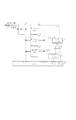
次に、信号処理回路部108について説明する。図5は、信号処理回路部108の構成を示すブロック図である。この信号処理回路部108には、読み出し用回路部107からのアナログ出力をディジタル変換するADコンバータ(ADC)7、2回分のオフセット成分(暗出力像)を格納する2つのオフセットメモリ1及び2が設けられている。また、放射線が照射された後の読み出し動作による信号値を格納する信号値メモリ3も設けられている。また、信号処理回路部108の全体を統括制御し、オフセットメモリ1及び2並びに信号値メモリ3に記憶されたデータに後述するような信号処理を施すCPU(中央演算処理装置)4が設けられている。更に、CPU4からのタイミングパルスが入力されるシフトレジスタ5、CPU4からのタイミングパルス及びシフトレジスタ5からの出力が入力される演算増幅器8並びに演算増幅器8からの出力が入力されるシフトレジスタ6が設けられている。
Next, the signal
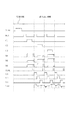
次に、本実施形態における読み取り動作(駆動方法)について説明する。図6は、読み取り動作を示すタイミングチャートである。ここでは、フレームNo.(フレーム数)が30であり、オフセット成分(FPN)取得と信号値取得とを交互に行う例を示す。紙面右側に向かう方向が時間の経過を意味する。このタイミングチャートでは、放射線照射期間を「X」で表し、読み出し期間を「H」で表している。即ち、「H」は、信号値の読み取り動作の期間であり、本読み期間又は本読み動作と称す。「W」はX線照射期間「X」と同じタイムスケールであるが、このタイミングではX線の照射を行わない。「W」は言わば光電変換素子のダークを蓄積している期間であり、ウェイト期間と称する。「K」及び「F」はそのウェイト期間の後の読み出し動作を示しており、検出回路部101の動作は読み出し期間「H」と何ら違いはない。「K」及び「F」は、互いに全く同じ読み出し動作であるが、その違いは、読み出し動作によって得られた信号を、放射線像を取得する情報として使用するか否かである。「K」は空読み(カラヨミ)期間又は空読み動作と称し、「F」はオフセット成分(FPN)読み取り期間又はオフセット成分(FPN)読み取り動作と称する。放射線像を取得する情報としては「F」が採用される。
Next, the reading operation (driving method) in the present embodiment will be described. FIG. 6 is a timing chart showing the reading operation. Here, frame No. An example is shown in which (the number of frames) is 30, and offset component (FPN) acquisition and signal value acquisition are alternately performed. The direction toward the right side of the page means the passage of time. In this timing chart, the radiation irradiation period is represented by “X”, and the readout period is represented by “H”. That is, “H” is a period of a signal value reading operation and is referred to as a main reading period or a main reading operation. “W” has the same time scale as the X-ray irradiation period “X”, but X-ray irradiation is not performed at this timing. “W” is a period during which dark of the photoelectric conversion element is accumulated, and is referred to as a wait period. “K” and “F” indicate a read operation after the wait period, and the operation of the
図6では、放射線爆射による信号値の取得と、オフセット成分の取得を交互に行っている。先ず、放射線撮像装置は、「W」と「K」とを交互に動作させる。この時、実際の撮影現場では、例えば、X線技師(撮影者)は、検出回路部101の受光面上で、患者(被撮影者)の撮影部位の位置合わせを行う。X線技師(撮影者)は、患者の位置合わせが終了し撮影の準備が整ったならば、装置の曝射命令を発する。曝射命令を受けた放射線撮像装置は、その時点のウェイト動作「W」と空読み動作「K」(便宜上「K」と書くが実際には「F」である。)を行い、その後「X」、「H」、「W」、「F」、「X」、・・・と交互に信号値及びオフセット成分の取得を行っていく。
In FIG. 6, acquisition of signal values by radiation explosion and acquisition of offset components are alternately performed. First, the radiation imaging apparatus operates “W” and “K” alternately. At this time, in an actual imaging field, for example, the X-ray technician (photographer) aligns the imaging region of the patient (photographed person) on the light receiving surface of the
次に、信号処理回路部108の動作について説明する。図7は、信号処理回路部108の動作を示すフローチャートである。図7の横軸は動画撮影のフレーム数を表しており、縦軸はフレーム毎の読み出し回路部107からの出力及び信号処理回路部108中での処理動作を表している。
Next, the operation of the signal
先ず、動画開始前(図6において「K」を行っているフレーム)では、シフトレジスタ5及び6を用いてゲートG11にタイミングパルスを送り、読み出し回路部107から信号処理回路部108に出力されるオフセット成分出力をオフセットメモリ1に格納する。そして、爆射命令が出るまで、オフセットメモリ1に読み出し回路部107から出力されるオフセット成分出力を上書きし続ける。爆射命令がなされると、その直後にX線の爆射が開始され、読み出し回路部107から信号値出力を取得する。
First, before the moving image is started (the frame in which “K” is performed in FIG. 6), a timing pulse is sent to the gate G11 using the shift registers 5 and 6, and is output from the
そして、シフトレジスタ5を用いてゲートG13にタイミングパルスを送り、得られた信号値を信号値メモリ3に格納する。次のフレームでは、前記同様にオフセット成分取得後にシフトレジスタ5及び6を用いてゲートG12にタイミングパルスを送り、読み出し回路部107から出力されたオフセット成分出力をオフセットメモリ2に格納する。この際に、CPU4において、オフセットメモリ1とオフセットメモリ2との信号を0.5で重み付けして加算することによって補正用の信号値を取得し、この補正用の信号値を信号値メモリの信号値から減算する。ここで、上記の単純な平均化処理を行う場合は、オフセットメモリ1とオフセットメモリ2との信号を加算し、信号値メモリの信号値を桁上げ(2倍)したものから減算処理するだけなのでCPU4への負荷が少ない。また、重み付けの重みに関して、オフセットメモリ1とオフセットメモリ2との信号を撮影のフレームレートに応じて重み付けを変えて加算する方法と、オフセットメモリ1とオフセットメモリ2との信号をフレームレートによらず一定の重み付けで加算する方法を選択できる。
Then, a timing pulse is sent to the gate G13 using the shift register 5, and the obtained signal value is stored in the
この減算値を補正値とする。そして、以後同様の手順で補正値を得る。 This subtraction value is used as a correction value. Thereafter, the correction value is obtained in the same procedure.
この補正法をX線画像の信号を取得する前後のオフセット成分を用いた補正であるので前後オフセット補正と称する。 Since this correction method is a correction using offset components before and after acquiring the X-ray image signal, it is referred to as front and rear offset correction.
なお、上述のように、これらの信号処理が行われている間の検出回路部101、駆動回路部(シフトレジスタ)103及び読み出し回路部107での信号処理は、図2及び図3に示す信号処理と同様である。
As described above, the signal processing in the
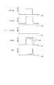
本実施形態によれば、従来の放射線撮像装置と比較して残像を著しく低減することができる。即ち、従来の放射線撮像装置では、矩形の光信号(X線信号)を受光した際は、矩形波入力直前及び直後に大きな残像が生じる。これに対し、本実施形態のように図7に示す信号処理を実施して、矩形の光信号を受光した場合には、図8A及び図8Bに示すように、残像が低減される。なお、図8Aには、矩形の光照射があった際の信号値、前後オフセット補正量、補正値及び残像についてフレーム数毎の信号値を表している。また、比較のために、図9に従来の放射線撮像装置において矩形の光照射があった際の信号値、オフセット成分補正量、補正値及び残像についてフレーム数毎の信号値を示す。 According to this embodiment, an afterimage can be significantly reduced as compared with a conventional radiation imaging apparatus. That is, in the conventional radiation imaging apparatus, when a rectangular optical signal (X-ray signal) is received, a large afterimage is generated immediately before and immediately after the input of the rectangular wave. On the other hand, when the signal processing shown in FIG. 7 is performed as in this embodiment and a rectangular optical signal is received, the afterimage is reduced as shown in FIGS. 8A and 8B. FIG. 8A shows signal values for each number of frames with respect to signal values, front and rear offset correction amounts, correction values, and afterimages when rectangular light irradiation is performed. For comparison, FIG. 9 shows signal values for each number of frames for signal values, offset component correction amounts, correction values, and afterimages when rectangular radiation is applied in the conventional radiation imaging apparatus.
特に、図8A及び図8Bにおいて、光照射(放射線照射)終了直後の残像について注目すると、従来の方法では予め取得したオフセット成分(FPN)を主とするオフセット成分出力で補正する。それに対し、本実施形態では、前後オフセット補正量として、放射線(X線)画像情報を有する信号値の直前及び直後に取得したオフセット成分出力を用いて補正用の信号値を取得し、それを用いて補正している。このため、放射線(光照射)終了後に放射線(光)入力がないにも拘わらず発生する残像成分を含む信号値を感知して正確に補正することができ、残像を著しく低減することができる。 In particular, in FIG. 8A and FIG. 8B, when attention is paid to the afterimage immediately after the end of light irradiation (radiation irradiation), the conventional method corrects the offset component (FPN) acquired in advance with the main offset component output. On the other hand, in the present embodiment, a correction signal value is acquired using an offset component output acquired immediately before and immediately after a signal value having radiation (X-ray) image information as a front-rear offset correction amount, and is used. Have been corrected. Therefore, a signal value including an afterimage component generated despite the absence of radiation (light) input after the end of radiation (light irradiation) can be sensed and corrected accurately, and the afterimage can be significantly reduced.
更に、図10A及び図10Bに示すように、動画撮影時のフレームレートが速ければ速いほど、残像が低減される。図10A及び図10Bでは、図8A及び図8Bと同様に、放射線(光)照射終了後に光入力がないにも拘わらず発生する残像成分を含む信号値に着目している。ここで図10A及び図10Bでは、撮影直前に取得したオフセット成分と撮影直後に取得したオフセット成分を1:1(0.5:0.5)で重み付け(平均化)して加算し、信号値から減算している。 Furthermore, as shown in FIGS. 10A and 10B, the higher the frame rate during moving image shooting, the lower the afterimage. In FIGS. 10A and 10B, as in FIGS. 8A and 8B, attention is paid to a signal value including an afterimage component that is generated even though there is no light input after the end of radiation (light) irradiation. Here, in FIGS. 10A and 10B, the offset component acquired immediately before shooting and the offset component acquired immediately after shooting are weighted (averaged) by 1: 1 (0.5: 0.5) and added to obtain a signal value. Is subtracted from.
ここで、フレームレートA(図10A)はフレームレートB(図10B)の2倍のフレームレートであり、フレームレートが速いフレームレートAで発生する残像は、フレームレートBに比べ少ないことがわかる。フレームレートが速くなると、残像成分を含む信号値が時間を追って変化するために、より短い時間内でオフセット成分出力の取得及び信号値の取得が行われ、短時間内で補正値が取得される。このことが残像の減少につながっているのである。従って、本実施形態で採用している補正方法(前後オフセット補正法)は、フレームレートを上げることで更に残像を削減することができるといえる。また、最適な重み付けを行うことによって、更に残像を削減できる。図10Cでは、フレームレートは、図10Aと同じであるが、撮影直前に取得したオフセット成分と撮影直後に取得したオフセット成分を3:7(0.3:0.7)で重み付けして加算して補正用の信号値を取得し、信号値から減算している。これにより図10Aに比べ、残像を更に削減できている。 Here, the frame rate A (FIG. 10A) is twice the frame rate of the frame rate B (FIG. 10B), and it can be seen that the afterimage generated at the frame rate A with a high frame rate is smaller than the frame rate B. When the frame rate increases, the signal value including the afterimage component changes with time, so that the offset component output and the signal value are acquired within a shorter time, and the correction value is acquired within a short time. . This has led to a reduction in afterimages. Therefore, it can be said that the afterimage can be further reduced by increasing the frame rate in the correction method (front-rear offset correction method) employed in this embodiment. Moreover, afterimages can be further reduced by performing optimum weighting. In FIG. 10C, the frame rate is the same as in FIG. 10A, but the offset component acquired immediately before shooting and the offset component acquired immediately after shooting are weighted and added by 3: 7 (0.3: 0.7). The signal value for correction is acquired and subtracted from the signal value. Thereby, the afterimage can be further reduced as compared with FIG. 10A.
本実施形態によって得る補正値に含まれるランダムノイズについて説明する。通常の読み取り動作で得られる信号値に含まれるランダムノイズの標準偏差をσ1、補正用読み取り動作で得られるオフセット成分出力に含まれるランダムノイズの標準偏差をσ2、撮影直前に取得したオフセット成分の重みをa、撮影直後に取得したオフセット成分の重みをbとすると、本実施形態による前後オフセット補正値に含まれるランダムノイズの標準偏差σtは、数2で表される。 The random noise included in the correction value obtained by this embodiment will be described. The standard deviation of random noise included in the signal value obtained in the normal reading operation is σ 1 , the standard deviation of random noise included in the offset component output obtained in the reading operation for correction is σ 2, and the offset component acquired immediately before imaging The standard deviation σ t of the random noise included in the front-rear offset correction value according to the present embodiment is expressed by the following equation (2).
特に、撮影直前に取得したオフセット成分と撮影直後に取得したオフセット成分を1:1(0.5:0.5)で重み付けして加算している場合は、数3で表される。
In particular, when the offset component acquired immediately before shooting and the offset component acquired immediately after shooting are weighted by 1: 1 (0.5: 0.5) and added, they are expressed by
従って、本実施形態によればランダムノイズを削減することもできる。 Therefore, according to the present embodiment, random noise can be reduced.
次に、本発明の実施形態に係る放射線撮像装置の放射線撮像システムへの応用例について説明する。図11は、放射線撮像システムの構成を示す模式図である。 Next, an application example of the radiation imaging apparatus according to the embodiment of the present invention to a radiation imaging system will be described. FIG. 11 is a schematic diagram illustrating a configuration of a radiation imaging system.
X線チューブ6050(X線源109)で発生したX線6060は患者又は被験者6061の胸部6062を透過し、本発明の実施形態に係る放射線撮像装置を内部に備えたイメージセンサ6040に入射する。イメージセンサ40に、上述の実施形態における検出回路部101、駆動回路部103、読み出し回路部107及び信号処理回路部108が含まれている。この入射したX線には患者6061の体の内部の情報が含まれている。X線の入射に対応してシンチレータ(蛍光体)は発光し、これを検出回路部101の光電変換素子が光電変換して、電気的情報を得る。イメージセンサ6040は、この情報を電気信号(デジタル信号)としてイメージプロセッサ6070に出力する。画像処理手段としてのイメージプロセッサ6070は、受信した信号に対して画像処理を施して、制御室の表示手段であるディスプレイ6080に出力する。ユーザは、ディスプレイ6080に表示された画像を観察して、患者6061の体の内部の情報を得ることができる。なお、イメージプロセッサ6070は、制御手段の機能も有しており、動画/静止画の撮影モードを切り換えたり、X線チューブ(放射線発生装置)6050の制御を行ったりすることも可能である。即ち、イメージプロセッサ6070は、上述の実施形態における制御ユニット105としても機能する。
The X-ray 6060 generated by the X-ray tube 6050 (X-ray source 109) passes through the chest 6062 of the patient or subject 6061 and enters the
また、イメージプロセッサ6070は、イメージセンサ6040から出力された電気信号を電話回線6090等の伝送処理手段を介して遠隔地へ転送し、ドクタールーム等の別の場所にある表示手段(ディスプレイ)6081に表示することもできる。また、イメージセンサ6040から出力された電気信号を光ディスク等の記録手段に保存し、この記録手段を用いて遠隔地の医師が診断することも可能である。また、記録手段となるフィルムプロセッサ6100によりフィルム6110に記録することもできる。
Further, the image processor 6070 transfers the electric signal output from the
なお、本発明の光電変換素子の構造は、特に限定されるものではない。例えば、アモルファスシリコンを主原料とし、放射線を可視光に変換する波長変換体からの可視光を吸収し電気信号に変換する光電変換素子が用いられてもよい。このような素子としては、例えば、アクセプタ不純物をドープしたP層と、真性半導体層であるI層と、ドナー不純物をドープしたN層と、を有するPIN型の光電変換素子があげられる。また、基板上に形成された金属薄膜層と、この金属薄膜層上に形成され、電子及び正孔の通過を阻止するアモルファス窒化シリコンからなる絶縁層と、この絶縁層上に形成された水素化アモルファスシリコンからなる半導体層と、この半導体層上に形成され、正孔の注入を阻止するN型の不純物半導体層と、この不純物半導体層上に形成された導電層と、を有するMIS型の光電変換素子等が挙げられる。MIS型の光電変換素子では、導電層は透明導電層であってもよく、また、導電層が注入阻止層上の一部に形成されていてもよい。変換素子として、これらの光電変換素子が用いられ、波長変換体が必要とされる場合、波長変換体としては、例えばGd2O2S、Gd2O3又はCsIを主成分とする蛍光体を用いることができる。更に、変換素子として、波長変換体を用いず半導体層の材料としてアモルファスセレン、ガリウム砒素、ヨウ化鉛又はヨウ化水銀を含有し、照射された放射線を吸収し直接電気信号に変換する素子を用いてもよい。 Note that the structure of the photoelectric conversion element of the present invention is not particularly limited. For example, a photoelectric conversion element that uses amorphous silicon as a main raw material and absorbs visible light from a wavelength converter that converts radiation into visible light and converts it into an electrical signal may be used. As such an element, for example, a PIN photoelectric conversion element having a P layer doped with an acceptor impurity, an I layer that is an intrinsic semiconductor layer, and an N layer doped with a donor impurity can be given. Also, a metal thin film layer formed on the substrate, an insulating layer formed on the metal thin film layer and made of amorphous silicon nitride for blocking the passage of electrons and holes, and a hydrogenation formed on the insulating layer A MIS type photoelectric layer having a semiconductor layer made of amorphous silicon, an N type impurity semiconductor layer formed on the semiconductor layer and blocking hole injection, and a conductive layer formed on the impurity semiconductor layer. A conversion element etc. are mentioned. In the MIS type photoelectric conversion element, the conductive layer may be a transparent conductive layer, or the conductive layer may be formed on a part of the injection blocking layer. When these photoelectric conversion elements are used as conversion elements and a wavelength converter is required, the wavelength converter is, for example, a phosphor mainly composed of Gd 2 O 2 S, Gd 2 O 3 or CsI. Can be used. Furthermore, as a conversion element, an element that does not use a wavelength converter and contains amorphous selenium, gallium arsenide, lead iodide or mercury iodide as a material of the semiconductor layer, and absorbs the irradiated radiation and directly converts it into an electrical signal is used. May be.
また、読み出し回路部107の構造も特に限定されるものではなく、例えば、検出回路部101から読み出した信号を増幅する増幅手段と、この増幅手段により増幅された信号を蓄積する蓄積手段と、この蓄積手段により蓄積された信号をシリアル変換するシリアル変換手段と、を有するものを用いることができる。
Further, the structure of the
なお、本発明の実施形態は、例えばコンピュータがプログラムを実行することによって実現することができる。また、プログラムをコンピュータに供給するための手段、例えばかかるプログラムを記録したCD−ROM等のコンピュータ読み取り可能な記録媒体又はかかるプログラムを伝送するインターネット等の伝送媒体も本発明の実施形態として適用することができる。また、上記のプログラムも本発明の実施形態として適用することができる。上記のプログラム、記録媒体、伝送媒体及びプログラムプロダクトは、本発明の範疇に含まれる。 The embodiment of the present invention can be realized by, for example, a computer executing a program. Also, means for supplying a program to a computer, for example, a computer-readable recording medium such as a CD-ROM recording such a program, or a transmission medium such as the Internet for transmitting such a program is also applied as an embodiment of the present invention. Can do. The above program can also be applied as an embodiment of the present invention. The above program, recording medium, transmission medium, and program product are included in the scope of the present invention.
本発明は、医療用の診断や工業用の非破壊検査等に用いて好適な放射線撮像装置に好適に用いられる。 The present invention is suitably used for a radiation imaging apparatus suitable for use in medical diagnosis, industrial nondestructive inspection, and the like.
1、2 オフセットメモリ
3 信号値メモリ
4 CPU
5、6 シフトレジスタ
7 ADコンバータ
8 演算増幅器
101 光電変換回路部
103 駆動回路部
105 制御ユニット
107 読み出し用回路部
108 信号処理回路部
109 X線源
S1−1〜S3−3 光電変換素子
T1−1〜T3−3 スイッチング素子
G1〜G3 ゲート駆動配線
M1〜M3 マトリクス信号配線
Vs 光電変換素子のバイアス線
CM1〜CM3 読み出し容量
RES1〜RES3 スイッチ
A1〜A3、B1〜B3、104 アンプ
Sn1〜Sn3 転送スイッチ
Sr1〜Sr3 読み出し用スイッチ
1, 2 Offset
5, 6
Claims (10)
前記検出部を駆動する駆動回路と、
前記検出部からの前記電荷に基づく電気信号を読み出す読み出し回路と、
前記検出部に放射線が照射されて行われる第1の蓄積動作と該第1の蓄積動作が行われた前記検出部を駆動して第1の信号値を読み取る第1の読み取り動作とを行う第1のフレーム動作と、該第1のフレーム動作の前に前記第1の蓄積動作と同じ長さの時間で前記検出部に放射線が照射されることなく行われる第2の蓄積動作と該第2の蓄積動作が行われた前記検出部を駆動して第2の信号値を読み取る第2の読み取り動作とを行う第2のフレーム動作と、前記第1のフレーム動作の後に前記第1の蓄積動作と同じ長さの時間で前記検出部に放射線が照射されることなく行われる第3の蓄積動作と該第3の蓄積動作が行われた前記検出部を駆動して第3の信号値を読み取る第3の読み取り動作とを行う第3のフレーム動作と、を選択的に実行する制御部と、
前記読み出し回路から出力された前記電気信号を処理する信号処理部と、を含み、
前記第1のフレーム動作と、前記第2のフレーム動作と、前記第3のフレーム動作と、が同じ撮影のフレームレートで行われ、
前記信号処理部は、前記第2の信号値と前記第3の信号値とを前記撮影のフレームレートの速さに応じた重み付けをして加算する処理をして得られた補正用の信号値を、前記第1の信号値から減算する放射線撮像装置。 A detection unit in which a plurality of conversion elements for converting radiation into electric charges are arranged two-dimensionally;
A drive circuit for driving the detection unit;
A readout circuit for reading out an electrical signal based on the charge from the detection unit;
A first accumulation operation performed by irradiating the detection unit with radiation and a first reading operation for reading the first signal value by driving the detection unit in which the first accumulation operation is performed. One frame operation, a second accumulation operation performed before the first frame operation is performed for the same length of time as the first accumulation operation without irradiation of the detection unit, and the second accumulation operation. A second frame operation for performing a second reading operation for reading the second signal value by driving the detection unit in which the accumulation operation is performed, and the first accumulation operation after the first frame operation. A third accumulation operation that is performed without irradiation of radiation to the detection unit in the same length of time, and the detection unit that has performed the third accumulation operation is driven to read a third signal value the third frame operation and performing a third read operation, the selectively executed And a control unit that,
A signal processing unit that processes the electrical signal output from the readout circuit,
The first frame operation, the second frame operation, and the third frame operation are performed at the same shooting frame rate,
Wherein the signal processing unit, the second signal value and said third signal value and the signal value of the correction obtained by the process of adding to the weighting according to the speed of the frame rate of the imaging the radiation imaging apparatus for subtracting from said first signal value.
2次元に複数配列された放射線を電荷に変換する変換素子を有する検出部に放射線が照射されて行われる第1の蓄積動作と該第1の蓄積動作が行われた前記検出部を駆動回路が駆動して読み出し回路が前記検出部から第1の信号値を読み取る第1の読み取り動作とを行う第1のフレーム動作と、該第1のフレーム動作の前に前記第1の蓄積動作と同じ長さの時間で前記検出部に放射線が照射されることなく行われる第2の蓄積動作と該第2の蓄積動作が行われた前記検出部を前記駆動回路が駆動して前記読み出し回路が前記検出部から第2の信号値を読み取る第2の読み取り動作とを行う第2のフレーム動作と、前記第1のフレーム動作の後に前記第1の蓄積動作と同じ長さの時間で前記検出部に放射線が照射されることなく行われる第3の蓄積動作と該第3の蓄積動作が行われた前記検出部を前記駆動回路が駆動して前記読み出し回路が前記検出部から第3の信号値を読み取る第3の読み取り動作とを行う第3のフレーム動作と、が同じ撮影のフレームレートで行われ、
前記読み出し回路から出力された前記電気信号を処理する信号処理部が、前記第2の信号値と前記第3の信号値とを前記撮影のフレームレートの速さに応じた重み付けをして加算する処理をして得られた補正用の信号値を、前記第1の信号値から減算する制御方法。 A control method for controlling the operation of a radiation imaging apparatus,
First accumulation operation and the detector driving circuit first accumulation operation is performed to perform the radiation which is arrayed two-dimensionally in the radiation is emitted in the detection unit to have a conversion element for converting the electric charge The first frame operation in which the reading circuit performs the first reading operation in which the reading circuit reads the first signal value from the detection unit, and the same as the first accumulation operation before the first frame operation The driving circuit drives the second accumulating operation performed without irradiating the detecting unit with radiation for a long time, and the detecting unit in which the second accumulating operation is performed. A second frame operation for performing a second reading operation for reading a second signal value from the detection unit and a time of the same length as the first accumulation operation after the first frame operation to the detection unit third radiation takes place without being irradiated Product operation and the third storage operation is performed with the detector of the drive circuit to the read circuit 3 which performs the third read operation of reading the third signal value from said detecting unit drive Frame operation is performed at the same shooting frame rate,
Signal processing unit for processing the electrical signals output from the readout circuit, for adding the second signal value and the third signal value by a weighting according to the speed of the frame rate of the imaging A control method for subtracting a correction signal value obtained by processing from the first signal value.
前記検出部に放射線が照射されて行われる第1の蓄積動作と該第1の蓄積動作が行われた前記検出部を前記駆動回路が駆動して前記読み出し回路が前記検出部から第1の信号値を読み取る第1の読み取り動作とを行う第1のフレーム動作と、該第1のフレーム動作の前に前記第1の蓄積動作と同じ長さの時間で前記検出部に放射線が照射されることなく行われる第2の蓄積動作と該第2の蓄積動作が行われた前記検出部を前記駆動回路が駆動して前記読み出し回路が前記検出部から第2の信号値を読み取る第2の読み取り動作とを行う第2のフレーム動作と、前記第1のフレーム動作の後に前記第1の蓄積動作と同じ長さの時間で前記検出部に放射線が照射されることなく行われる第3の蓄積動作と該第3の蓄積動作が行われた前記検出部を前記駆動回路が駆動して前記読み出し回路が前記検出部から第3の信号値を読み取る第3の読み取り動作とを行う第3のフレーム動作と、が同じ撮影のフレームレートで行われるようにコンピュータに選択的に実行させ、
前記信号処理部が前記第2の信号値と前記第3の信号値とを前記撮影のフレームレートの速さに応じた重み付けをして加算する処理をして得られた補正用の信号値を、前記第1の信号値から減算する手順をコンピュータに実行させることを特徴とするプログラム。 A detection unit in which a plurality of conversion elements that convert radiation into charges are two-dimensionally arranged; a drive circuit that drives the detection unit; a readout circuit that reads an electrical signal based on the charge from the detection unit; A program stored in a storage medium for causing a computer to control the operation of a radiation imaging apparatus comprising: a signal processing unit that processes the electrical signal output from a readout circuit;
A first accumulation operation performed by irradiating the detection unit with radiation, and the detection circuit that has performed the first accumulation operation is driven by the drive circuit, and the readout circuit receives a first signal from the detection unit. A first frame operation for performing a first reading operation for reading a value, and the detection unit is irradiated with radiation for the same length of time as the first accumulation operation before the first frame operation . second read operation performed second accumulation operation and the said detection unit which second storing operation is performed wherein the drive circuit drives the readout circuit is to read the second signal value from the detection unit without And a third accumulation operation that is performed without irradiating the detection unit with the same length of time as the first accumulation operation after the first frame operation. the detection unit storing operation of the third was made The third frame operation of the serial driver circuit the read circuit is driven to perform a third read operation of reading the third signal value from said detecting unit, but the computer as is done at a frame rate of the same shooting Selectively run,
The signal value of the correction obtained by the process of adding to the weight of the signal processing unit in accordance with said third signal value and the second signal value on the speed of the frame rate of the imaging , a program for causing the steps of subtracting from the first signal value to the computer.
Priority Applications (2)
| Application Number | Priority Date | Filing Date | Title |
|---|---|---|---|
| JP2006215855A JP4965931B2 (en) | 2005-08-17 | 2006-08-08 | Radiation imaging apparatus, radiation imaging system, control method thereof, and control program |
| US11/502,541 US7573038B2 (en) | 2005-08-17 | 2006-08-11 | Radiation image pickup apparatus, radiation image pickup system, their control method and their control program |
Applications Claiming Priority (3)
| Application Number | Priority Date | Filing Date | Title |
|---|---|---|---|
| JP2005236773 | 2005-08-17 | ||
| JP2005236773 | 2005-08-17 | ||
| JP2006215855A JP4965931B2 (en) | 2005-08-17 | 2006-08-08 | Radiation imaging apparatus, radiation imaging system, control method thereof, and control program |
Publications (3)
| Publication Number | Publication Date |
|---|---|
| JP2007075598A JP2007075598A (en) | 2007-03-29 |
| JP2007075598A5 JP2007075598A5 (en) | 2009-09-17 |
| JP4965931B2 true JP4965931B2 (en) | 2012-07-04 |
Family
ID=37766601
Family Applications (1)
| Application Number | Title | Priority Date | Filing Date |
|---|---|---|---|
| JP2006215855A Expired - Fee Related JP4965931B2 (en) | 2005-08-17 | 2006-08-08 | Radiation imaging apparatus, radiation imaging system, control method thereof, and control program |
Country Status (2)
| Country | Link |
|---|---|
| US (1) | US7573038B2 (en) |
| JP (1) | JP4965931B2 (en) |
Families Citing this family (73)
| Publication number | Priority date | Publication date | Assignee | Title |
|---|---|---|---|---|
| JP2005175418A (en) * | 2003-11-19 | 2005-06-30 | Canon Inc | Photoelectric conversion apparatus |
| JP5058517B2 (en) | 2005-06-14 | 2012-10-24 | キヤノン株式会社 | Radiation imaging apparatus, control method therefor, and radiation imaging system |
| WO2007026419A1 (en) * | 2005-08-31 | 2007-03-08 | Shimadzu Corporation | Radiation imaging device and radiation detection signal processing method |
| JP4750512B2 (en) * | 2005-09-01 | 2011-08-17 | キヤノン株式会社 | Radiation imaging apparatus, control method therefor, and radiation imaging system |
| JP5317388B2 (en) * | 2005-09-30 | 2013-10-16 | キヤノン株式会社 | Radiation imaging apparatus, radiation imaging system, and program |
| JP2007104219A (en) | 2005-10-03 | 2007-04-19 | Canon Inc | Radiation photography instrument and its control method, radiation photography system |
| JP4834518B2 (en) | 2005-11-29 | 2011-12-14 | キヤノン株式会社 | Radiation imaging apparatus, control method therefor, and recording medium on which program for executing the same is recorded |
| JP2007151761A (en) | 2005-12-02 | 2007-06-21 | Canon Inc | Apparatus, system, method, and program for radiation imaging |
| JP4989197B2 (en) * | 2005-12-13 | 2012-08-01 | キヤノン株式会社 | Radiation imaging apparatus, radiation imaging system, and correction method |
| JP4891096B2 (en) * | 2006-01-30 | 2012-03-07 | キヤノン株式会社 | Radiation imaging device |
| JP5043448B2 (en) * | 2006-03-10 | 2012-10-10 | キヤノン株式会社 | Radiation imaging apparatus and radiation imaging system |
| JP4850730B2 (en) * | 2006-03-16 | 2012-01-11 | キヤノン株式会社 | Imaging apparatus, processing method thereof, and program |
| JP4868926B2 (en) * | 2006-04-21 | 2012-02-01 | キヤノン株式会社 | Radiation imaging device |
| JP4847202B2 (en) * | 2006-04-27 | 2011-12-28 | キヤノン株式会社 | Imaging apparatus and radiation imaging system |
| JP4989120B2 (en) * | 2006-06-16 | 2012-08-01 | キヤノン株式会社 | Radiation imaging system and driving method thereof |
| JP5159161B2 (en) * | 2006-06-26 | 2013-03-06 | キヤノン株式会社 | Radiation imaging apparatus, radiation imaging system and control method thereof |
| JP5038031B2 (en) | 2006-07-11 | 2012-10-03 | キヤノン株式会社 | Radiography apparatus, driving method thereof and radiation imaging system |
| JP2008042478A (en) * | 2006-08-04 | 2008-02-21 | Canon Inc | Imaging device, radiation ray imaging device and its driving method |
| JP5300216B2 (en) * | 2006-08-29 | 2013-09-25 | キヤノン株式会社 | Electronic cassette type radiation detector |
| JP4986771B2 (en) * | 2006-08-31 | 2012-07-25 | キヤノン株式会社 | Imaging apparatus, driving method thereof, and radiation imaging system |
| JP5121473B2 (en) * | 2007-02-01 | 2013-01-16 | キヤノン株式会社 | Radiation imaging apparatus, control method therefor, and radiation imaging system |
| US7929035B2 (en) * | 2007-03-08 | 2011-04-19 | Imagerlabs, Inc. | Ultra low noise CMOS imager |
| US7869568B2 (en) * | 2007-03-13 | 2011-01-11 | Canon Kabushiki Kaisha | Radiation imaging apparatus, and method and program for controlling radiation imaging apparatus |
| KR101393633B1 (en) * | 2007-10-31 | 2014-05-09 | 삼성디스플레이 주식회사 | X-ray detecting panel, x-ray detector and driving method of x-ray detector |
| JP2009141439A (en) * | 2007-12-03 | 2009-06-25 | Canon Inc | Radiation imaging apparatus, driving method thereof, and program |
| JP5311834B2 (en) | 2008-01-24 | 2013-10-09 | キヤノン株式会社 | Imaging apparatus, imaging system, signal processing method, and program |
| JP5274098B2 (en) | 2008-04-30 | 2013-08-28 | キヤノン株式会社 | Imaging apparatus, radiation imaging system, control method thereof, and program |
| JP5195907B2 (en) * | 2008-05-14 | 2013-05-15 | コニカミノルタエムジー株式会社 | Dynamic image photographing control device and dynamic image photographing system |
| FR2932051B1 (en) * | 2008-05-27 | 2010-06-18 | Trixell | SYNCHRONIZATION METHOD FOR WIRELESS CONNECTION AND RADIOLOGICAL SYSTEM USING SUCH A METHOD |
| JP2010034661A (en) * | 2008-07-25 | 2010-02-12 | Shimadzu Corp | Imaging device |
| KR101571044B1 (en) | 2008-12-24 | 2015-11-24 | 삼성디스플레이 주식회사 | X-ray detector and driving method of the same |
| JP5792923B2 (en) | 2009-04-20 | 2015-10-14 | キヤノン株式会社 | Radiation imaging apparatus, radiation imaging system, control method thereof, and program thereof |
| JP5377081B2 (en) * | 2009-06-01 | 2013-12-25 | キヤノン株式会社 | Radiation imaging apparatus and control method thereof |
| JP5867980B2 (en) * | 2009-06-02 | 2016-02-24 | キヤノン株式会社 | X-ray fluoroscopic equipment |
| JP5439984B2 (en) * | 2009-07-03 | 2014-03-12 | ソニー株式会社 | Photoelectric conversion device and radiation imaging device |
| JP5418599B2 (en) * | 2009-10-21 | 2014-02-19 | 株式会社島津製作所 | Radiation imaging device |
| JP5176081B2 (en) * | 2010-01-18 | 2013-04-03 | 株式会社吉田製作所 | X-ray imaging method and X-ray imaging apparatus |
| CN102934423B (en) * | 2010-06-03 | 2016-04-06 | 柯尼卡美能达医疗印刷器材株式会社 | Radiographic imaging device |
| JP5672853B2 (en) * | 2010-08-25 | 2015-02-18 | ソニー株式会社 | Radiation imaging device |
| JP5776693B2 (en) * | 2010-09-09 | 2015-09-09 | コニカミノルタ株式会社 | Radiographic imaging apparatus and radiographic imaging system |
| KR101753895B1 (en) * | 2010-12-03 | 2017-07-05 | 삼성디스플레이 주식회사 | A X-ray detector and a method for driving the same |
| WO2013098985A1 (en) * | 2011-12-28 | 2013-07-04 | キヤノン株式会社 | Image pickup device, image pickup system, and control method for image pickup device |
| JP5986526B2 (en) | 2012-04-06 | 2016-09-06 | キヤノン株式会社 | Radiation imaging apparatus, control method therefor, and radiation imaging system |
| KR102069683B1 (en) * | 2012-08-24 | 2020-01-23 | 가부시키가이샤 한도오따이 에네루기 켄큐쇼 | Radiation detection panel, radiation imaging device, and diagnostic imaging device |
| JP5934128B2 (en) | 2013-02-28 | 2016-06-15 | キヤノン株式会社 | Radiation imaging apparatus and radiation imaging system |
| JP6016673B2 (en) | 2013-02-28 | 2016-10-26 | キヤノン株式会社 | Radiation imaging apparatus and radiation imaging system |
| JP5986524B2 (en) | 2013-02-28 | 2016-09-06 | キヤノン株式会社 | Radiation imaging apparatus and radiation imaging system |
| JP6161346B2 (en) | 2013-03-19 | 2017-07-12 | キヤノン株式会社 | Imaging system |
| JP6238577B2 (en) | 2013-06-05 | 2017-11-29 | キヤノン株式会社 | Radiation imaging apparatus and radiation imaging system |
| US9554759B2 (en) * | 2013-09-18 | 2017-01-31 | Carestream Health, Inc. | Digital radiography detector image readout process |
| JP6305008B2 (en) * | 2013-10-21 | 2018-04-04 | キヤノン株式会社 | Radiation imaging apparatus and control method thereof, radiographic image processing apparatus and method, program, and computer-readable storage medium |
| JP6463136B2 (en) | 2014-02-14 | 2019-01-30 | キヤノン株式会社 | Radiation detection apparatus and radiation detection system |
| JP6339853B2 (en) | 2014-05-01 | 2018-06-06 | キヤノン株式会社 | Radiation imaging apparatus and radiation imaging system |
| JP6595803B2 (en) | 2014-06-13 | 2019-10-23 | キヤノン株式会社 | Radiation imaging apparatus, radiation imaging system and control method thereof |
| JP6391388B2 (en) | 2014-09-24 | 2018-09-19 | キヤノン株式会社 | Radiation imaging device |
| US10470735B2 (en) | 2014-12-03 | 2019-11-12 | Koninklijke Philips N.V. | Device and method for signal compensation in medical X-ray images |
| JP6570315B2 (en) | 2015-05-22 | 2019-09-04 | キヤノン株式会社 | Radiation imaging apparatus and radiation imaging system |
| JP6573377B2 (en) | 2015-07-08 | 2019-09-11 | キヤノン株式会社 | Radiation imaging apparatus, control method thereof, and program |
| JP6573378B2 (en) | 2015-07-10 | 2019-09-11 | キヤノン株式会社 | Radiation imaging apparatus, control method thereof, and program |
| JP6626301B2 (en) | 2015-09-28 | 2019-12-25 | キヤノン株式会社 | Radiation imaging apparatus, radiation imaging system, control method of radiation imaging apparatus, and program |
| JP6587517B2 (en) | 2015-11-13 | 2019-10-09 | キヤノン株式会社 | Radiation imaging system |
| JP6663210B2 (en) | 2015-12-01 | 2020-03-11 | キヤノン株式会社 | Radiation imaging apparatus and control method thereof |
| WO2017132633A1 (en) * | 2016-01-29 | 2017-08-03 | Varex Imaging Corporation | Row driver fault isolation circuitry for matrix type integrated circuit |
| JP6706963B2 (en) | 2016-04-18 | 2020-06-10 | キヤノン株式会社 | Radiation imaging apparatus, radiation imaging system, and control method for radiation imaging apparatus |
| JP6871717B2 (en) | 2016-11-10 | 2021-05-12 | キヤノン株式会社 | Radiation imaging device, radiation imaging system and radiation imaging method |
| JP6853729B2 (en) | 2017-05-08 | 2021-03-31 | キヤノン株式会社 | Radiation imaging device, radiation imaging system, control method and program of radiation imaging device |
| WO2019012846A1 (en) | 2017-07-10 | 2019-01-17 | キヤノン株式会社 | Radiation imaging device and radiation imaging system |
| CN107863353A (en) * | 2017-09-25 | 2018-03-30 | 惠科股份有限公司 | A kind of manufacture method of array base palte and array base palte |
| JP7067912B2 (en) | 2017-12-13 | 2022-05-16 | キヤノン株式会社 | Radiation imaging device and radiation imaging system |
| JP6818724B2 (en) | 2018-10-01 | 2021-01-20 | キヤノン株式会社 | Radiation imaging device, its control method and radiation imaging system |
| JP7170497B2 (en) | 2018-10-22 | 2022-11-14 | キヤノン株式会社 | Radiation imaging device and radiation imaging system |
| JP7361516B2 (en) | 2019-07-12 | 2023-10-16 | キヤノン株式会社 | Radiography device, radiography system, radiography device control method, and program |
| JP7449260B2 (en) | 2021-04-15 | 2024-03-13 | キヤノン株式会社 | Radiation imaging device and radiation imaging system |
Family Cites Families (30)
| Publication number | Priority date | Publication date | Assignee | Title |
|---|---|---|---|---|
| JP4035194B2 (en) * | 1996-03-13 | 2008-01-16 | キヤノン株式会社 | X-ray detection apparatus and X-ray detection system |
| DE19631624C1 (en) * | 1996-08-05 | 1997-10-23 | Siemens Ag | Diagnostic X-ray apparatus with phantom image correction |
| JP3815755B2 (en) * | 1997-01-17 | 2006-08-30 | キヤノン株式会社 | Imaging method and imaging apparatus |
| JP4029491B2 (en) * | 1998-09-03 | 2008-01-09 | 株式会社島津製作所 | X-ray imaging device |
| US6453008B1 (en) * | 1999-07-29 | 2002-09-17 | Kabushiki Kaisha Toshiba | Radiation detector noise reduction method and radiation detector |
| JP4828687B2 (en) * | 1999-07-29 | 2011-11-30 | 東芝医用システムエンジニアリング株式会社 | Radiation detector noise reduction method and radiation diagnostic apparatus |
| US6952015B2 (en) * | 2001-07-30 | 2005-10-04 | Canon Kabushiki Kaisha | Image pick-up apparatus and image pick-up system |
| DE10213564A1 (en) * | 2002-03-26 | 2003-10-16 | Siemens Ag | Method for suppressing ghosting in X-ray pictures applies a subtraction process to correct an X-ray shot by processing residual image portions |
| JP2004020300A (en) * | 2002-06-14 | 2004-01-22 | Toshiba Corp | Radiation diagnostic device |
| US6904126B2 (en) * | 2002-06-19 | 2005-06-07 | Canon Kabushiki Kaisha | Radiological imaging apparatus and method |
| JP4258832B2 (en) * | 2002-12-24 | 2009-04-30 | 株式会社日立メディコ | X-ray diagnostic imaging equipment |
| JP4307138B2 (en) * | 2003-04-22 | 2009-08-05 | キヤノン株式会社 | Photoelectric conversion device and control method of photoelectric conversion device |
| JP4669653B2 (en) | 2003-04-22 | 2011-04-13 | キヤノン株式会社 | Radiation imaging apparatus, radiation imaging system, and computer program |
| JP2004344249A (en) * | 2003-05-20 | 2004-12-09 | Canon Inc | Radiographic apparatus, radiographic method, and program and recording medium for radiography |
| JP2006526925A (en) * | 2003-06-05 | 2006-11-24 | コーニンクレッカ フィリップス エレクトロニクス エヌ ヴィ | Detector for detection of X-ray radiation |
| US7215801B2 (en) * | 2003-06-05 | 2007-05-08 | General Electric Company | Method, system and apparatus for processing radiographic images of scanned objects |
| DE10334818A1 (en) * | 2003-07-30 | 2005-03-03 | Siemens Ag | X-ray detector |
| JP2005175418A (en) * | 2003-11-19 | 2005-06-30 | Canon Inc | Photoelectric conversion apparatus |
| JP4533010B2 (en) | 2003-11-20 | 2010-08-25 | キヤノン株式会社 | Radiation imaging apparatus, radiation imaging method, and radiation imaging system |
| JP4307230B2 (en) * | 2003-12-05 | 2009-08-05 | キヤノン株式会社 | Radiation imaging apparatus and radiation imaging method |
| JP4441294B2 (en) * | 2004-03-12 | 2010-03-31 | キヤノン株式会社 | Radiation imaging apparatus and control method thereof |
| JP4469638B2 (en) * | 2004-03-12 | 2010-05-26 | キヤノン株式会社 | Reading device and image photographing device |
| JP2005287773A (en) | 2004-03-31 | 2005-10-20 | Canon Inc | Image photography apparatus and image photography system |
| US7403594B2 (en) | 2004-03-31 | 2008-07-22 | Canon Kabushiki Kaisha | Radiation imaging apparatus and control method therefor |
| JP4307322B2 (en) | 2004-05-18 | 2009-08-05 | キヤノン株式会社 | Radiation imaging apparatus and radiation imaging system |
| JP5058517B2 (en) * | 2005-06-14 | 2012-10-24 | キヤノン株式会社 | Radiation imaging apparatus, control method therefor, and radiation imaging system |
| JP4750512B2 (en) | 2005-09-01 | 2011-08-17 | キヤノン株式会社 | Radiation imaging apparatus, control method therefor, and radiation imaging system |
| JP5317388B2 (en) | 2005-09-30 | 2013-10-16 | キヤノン株式会社 | Radiation imaging apparatus, radiation imaging system, and program |
| JP2007151761A (en) | 2005-12-02 | 2007-06-21 | Canon Inc | Apparatus, system, method, and program for radiation imaging |
| JP4989197B2 (en) | 2005-12-13 | 2012-08-01 | キヤノン株式会社 | Radiation imaging apparatus, radiation imaging system, and correction method |
-
2006
- 2006-08-08 JP JP2006215855A patent/JP4965931B2/en not_active Expired - Fee Related
- 2006-08-11 US US11/502,541 patent/US7573038B2/en not_active Expired - Fee Related
Also Published As
| Publication number | Publication date |
|---|---|
| US7573038B2 (en) | 2009-08-11 |
| US20070040099A1 (en) | 2007-02-22 |
| JP2007075598A (en) | 2007-03-29 |
Similar Documents
| Publication | Publication Date | Title |
|---|---|---|
| JP4965931B2 (en) | Radiation imaging apparatus, radiation imaging system, control method thereof, and control program | |
| US8247779B2 (en) | Radiation imaging apparatus, its control method, and radiation imaging system | |
| US7408167B2 (en) | Imaging apparatus, radiation imaging apparatus, and radiation imaging system | |
| JP3839941B2 (en) | Radiation detection apparatus and radiation detection method | |
| US7227926B2 (en) | Imaging apparatus and imaging system | |
| US7302039B2 (en) | Radiography apparatus, radiography system, and control method thereof | |
| JP5171431B2 (en) | Photoelectric conversion device, radiation imaging device, and radiation detection device | |
| JP5459066B2 (en) | Radiation imaging equipment | |
| JP2009141439A (en) | Radiation imaging apparatus, driving method thereof, and program | |
| US7127031B2 (en) | Radiation imaging apparatus, radiation imaging system and radiation imaging method | |
| JP4739060B2 (en) | Radiation imaging apparatus, radiation imaging system, and control method thereof | |
| JP5509032B2 (en) | Radiation image detector | |
| WO2018135293A1 (en) | Radiation imaging device and radiation imaging system | |
| JP3740435B2 (en) | Radiation imaging apparatus, driving method thereof, and radiation imaging system | |
| JP4872017B2 (en) | Imaging apparatus, driving method thereof, radiation imaging apparatus, and radiation imaging system using the same | |
| JP4314073B2 (en) | Radiation imaging apparatus and radiation imaging method | |
| JP5028545B2 (en) | Imaging apparatus, radiation imaging apparatus, and radiation imaging system using the same | |
| JP4921581B2 (en) | Imaging apparatus, radiation imaging apparatus, and radiation imaging system using the same | |
| JP2006128644A (en) | Imaging apparatus, radiation imaging apparatus, and radiation imaging system | |
| JP2011247605A (en) | Radiation image photographing device and radiation image processing system | |
| JP4546560B2 (en) | Radiation imaging apparatus, driving method thereof, and radiation imaging system | |
| JP5258940B2 (en) | Imaging apparatus and radiation imaging system | |
| JP5673487B2 (en) | Radiation imaging equipment | |
| JP2020081325A (en) | Radiation detector | |
| JP2018195949A (en) | Radiation imaging device and radiation imaging system |
Legal Events
| Date | Code | Title | Description |
|---|---|---|---|
| A521 | Request for written amendment filed |
Free format text: JAPANESE INTERMEDIATE CODE: A523 Effective date: 20090805 |
|
| A621 | Written request for application examination |
Free format text: JAPANESE INTERMEDIATE CODE: A621 Effective date: 20090805 |
|
| RD04 | Notification of resignation of power of attorney |
Free format text: JAPANESE INTERMEDIATE CODE: A7424 Effective date: 20100201 |
|
| RD01 | Notification of change of attorney |
Free format text: JAPANESE INTERMEDIATE CODE: A7421 Effective date: 20100630 |
|
| A977 | Report on retrieval |
Free format text: JAPANESE INTERMEDIATE CODE: A971007 Effective date: 20110721 |
|
| A131 | Notification of reasons for refusal |
Free format text: JAPANESE INTERMEDIATE CODE: A131 Effective date: 20110726 |
|
| A521 | Request for written amendment filed |
Free format text: JAPANESE INTERMEDIATE CODE: A523 Effective date: 20110914 |
|
| TRDD | Decision of grant or rejection written | ||
| A01 | Written decision to grant a patent or to grant a registration (utility model) |
Free format text: JAPANESE INTERMEDIATE CODE: A01 Effective date: 20120327 |
|
| A01 | Written decision to grant a patent or to grant a registration (utility model) |
Free format text: JAPANESE INTERMEDIATE CODE: A01 |
|
| A61 | First payment of annual fees (during grant procedure) |
Free format text: JAPANESE INTERMEDIATE CODE: A61 Effective date: 20120330 |
|
| R151 | Written notification of patent or utility model registration |
Ref document number: 4965931 Country of ref document: JP Free format text: JAPANESE INTERMEDIATE CODE: R151 |
|
| FPAY | Renewal fee payment (event date is renewal date of database) |
Free format text: PAYMENT UNTIL: 20150406 Year of fee payment: 3 |
|
| LAPS | Cancellation because of no payment of annual fees |