JP2005175418A - Photoelectric conversion apparatus - Google Patents
Photoelectric conversion apparatus Download PDFInfo
- Publication number
- JP2005175418A JP2005175418A JP2004180899A JP2004180899A JP2005175418A JP 2005175418 A JP2005175418 A JP 2005175418A JP 2004180899 A JP2004180899 A JP 2004180899A JP 2004180899 A JP2004180899 A JP 2004180899A JP 2005175418 A JP2005175418 A JP 2005175418A
- Authority
- JP
- Japan
- Prior art keywords
- photoelectric conversion
- transistor
- constant current
- current source
- source
- Prior art date
- Legal status (The legal status is an assumption and is not a legal conclusion. Google has not performed a legal analysis and makes no representation as to the accuracy of the status listed.)
- Pending
Links
- 238000006243 chemical reaction Methods 0.000 title claims abstract description 99
- 239000010409 thin film Substances 0.000 claims description 31
- 238000003384 imaging method Methods 0.000 claims description 29
- 229910021417 amorphous silicon Inorganic materials 0.000 claims description 19
- 230000005855 radiation Effects 0.000 claims description 10
- OAICVXFJPJFONN-UHFFFAOYSA-N Phosphorus Chemical compound [P] OAICVXFJPJFONN-UHFFFAOYSA-N 0.000 claims description 8
- 229910021420 polycrystalline silicon Inorganic materials 0.000 claims description 8
- 229920005591 polysilicon Polymers 0.000 claims description 8
- JBRZTFJDHDCESZ-UHFFFAOYSA-N AsGa Chemical compound [As]#[Ga] JBRZTFJDHDCESZ-UHFFFAOYSA-N 0.000 claims description 2
- 229910001218 Gallium arsenide Inorganic materials 0.000 claims description 2
- BUGBHKTXTAQXES-UHFFFAOYSA-N Selenium Chemical compound [Se] BUGBHKTXTAQXES-UHFFFAOYSA-N 0.000 claims description 2
- XMBWDFGMSWQBCA-UHFFFAOYSA-N hydrogen iodide Chemical compound I XMBWDFGMSWQBCA-UHFFFAOYSA-N 0.000 claims description 2
- 239000000463 material Substances 0.000 claims description 2
- QKEOZZYXWAIQFO-UHFFFAOYSA-M mercury(1+);iodide Chemical compound [Hg]I QKEOZZYXWAIQFO-UHFFFAOYSA-M 0.000 claims description 2
- 229910052711 selenium Inorganic materials 0.000 claims description 2
- 239000011669 selenium Substances 0.000 claims description 2
- 229910004613 CdTe Inorganic materials 0.000 claims 1
- 229910004611 CdZnTe Inorganic materials 0.000 claims 1
- 229910005540 GaP Inorganic materials 0.000 claims 1
- HZXMRANICFIONG-UHFFFAOYSA-N gallium phosphide Chemical compound [Ga]#P HZXMRANICFIONG-UHFFFAOYSA-N 0.000 claims 1
- 230000003071 parasitic effect Effects 0.000 abstract description 14
- 230000000694 effects Effects 0.000 abstract description 6
- 239000010410 layer Substances 0.000 description 24
- 238000010586 diagram Methods 0.000 description 17
- 239000011521 glass Substances 0.000 description 13
- 239000000758 substrate Substances 0.000 description 13
- 239000003990 capacitor Substances 0.000 description 11
- 101100136063 Mycobacterium tuberculosis (strain ATCC 25618 / H37Rv) PE11 gene Proteins 0.000 description 8
- 239000010408 film Substances 0.000 description 8
- 230000035945 sensitivity Effects 0.000 description 5
- 239000004065 semiconductor Substances 0.000 description 4
- XQPRBTXUXXVTKB-UHFFFAOYSA-M caesium iodide Chemical compound [I-].[Cs+] XQPRBTXUXXVTKB-UHFFFAOYSA-M 0.000 description 2
- 229910021419 crystalline silicon Inorganic materials 0.000 description 2
- 230000020169 heat generation Effects 0.000 description 2
- 238000005224 laser annealing Methods 0.000 description 2
- 239000011159 matrix material Substances 0.000 description 2
- HQVNEWCFYHHQES-UHFFFAOYSA-N silicon nitride Chemical compound N12[Si]34N5[Si]62N3[Si]51N64 HQVNEWCFYHHQES-UHFFFAOYSA-N 0.000 description 2
- 102100040862 Dual specificity protein kinase CLK1 Human genes 0.000 description 1
- 102100040844 Dual specificity protein kinase CLK2 Human genes 0.000 description 1
- 229910052688 Gadolinium Inorganic materials 0.000 description 1
- 101000749294 Homo sapiens Dual specificity protein kinase CLK1 Proteins 0.000 description 1
- 101000749291 Homo sapiens Dual specificity protein kinase CLK2 Proteins 0.000 description 1
- 238000009825 accumulation Methods 0.000 description 1
- 239000012790 adhesive layer Substances 0.000 description 1
- 230000005540 biological transmission Effects 0.000 description 1
- 238000003745 diagnosis Methods 0.000 description 1
- UIWYJDYFSGRHKR-UHFFFAOYSA-N gadolinium atom Chemical compound [Gd] UIWYJDYFSGRHKR-UHFFFAOYSA-N 0.000 description 1
- 239000012535 impurity Substances 0.000 description 1
- 238000010030 laminating Methods 0.000 description 1
- 238000004519 manufacturing process Methods 0.000 description 1
- 238000000034 method Methods 0.000 description 1
- 230000003287 optical effect Effects 0.000 description 1
- 239000011241 protective layer Substances 0.000 description 1
- 238000000926 separation method Methods 0.000 description 1
Images


Classifications
-
- H—ELECTRICITY
- H01—ELECTRIC ELEMENTS
- H01L—SEMICONDUCTOR DEVICES NOT COVERED BY CLASS H10
- H01L27/00—Devices consisting of a plurality of semiconductor or other solid-state components formed in or on a common substrate
- H01L27/14—Devices consisting of a plurality of semiconductor or other solid-state components formed in or on a common substrate including semiconductor components sensitive to infrared radiation, light, electromagnetic radiation of shorter wavelength or corpuscular radiation and specially adapted either for the conversion of the energy of such radiation into electrical energy or for the control of electrical energy by such radiation
- H01L27/144—Devices controlled by radiation
- H01L27/146—Imager structures
- H01L27/14643—Photodiode arrays; MOS imagers
- H01L27/14658—X-ray, gamma-ray or corpuscular radiation imagers
-
- H—ELECTRICITY
- H04—ELECTRIC COMMUNICATION TECHNIQUE
- H04N—PICTORIAL COMMUNICATION, e.g. TELEVISION
- H04N25/00—Circuitry of solid-state image sensors [SSIS]; Control thereof
- H04N25/60—Noise processing, e.g. detecting, correcting, reducing or removing noise
- H04N25/67—Noise processing, e.g. detecting, correcting, reducing or removing noise applied to fixed-pattern noise, e.g. non-uniformity of response
- H04N25/671—Noise processing, e.g. detecting, correcting, reducing or removing noise applied to fixed-pattern noise, e.g. non-uniformity of response for non-uniformity detection or correction
- H04N25/677—Noise processing, e.g. detecting, correcting, reducing or removing noise applied to fixed-pattern noise, e.g. non-uniformity of response for non-uniformity detection or correction for reducing the column or line fixed pattern noise
-
- H—ELECTRICITY
- H04—ELECTRIC COMMUNICATION TECHNIQUE
- H04N—PICTORIAL COMMUNICATION, e.g. TELEVISION
- H04N25/00—Circuitry of solid-state image sensors [SSIS]; Control thereof
- H04N25/70—SSIS architectures; Circuits associated therewith
- H04N25/71—Charge-coupled device [CCD] sensors; Charge-transfer registers specially adapted for CCD sensors
- H04N25/75—Circuitry for providing, modifying or processing image signals from the pixel array
-
- H—ELECTRICITY
- H04—ELECTRIC COMMUNICATION TECHNIQUE
- H04N—PICTORIAL COMMUNICATION, e.g. TELEVISION
- H04N25/00—Circuitry of solid-state image sensors [SSIS]; Control thereof
- H04N25/70—SSIS architectures; Circuits associated therewith
- H04N25/76—Addressed sensors, e.g. MOS or CMOS sensors
-
- H—ELECTRICITY
- H04—ELECTRIC COMMUNICATION TECHNIQUE
- H04N—PICTORIAL COMMUNICATION, e.g. TELEVISION
- H04N5/00—Details of television systems
- H04N5/30—Transforming light or analogous information into electric information
- H04N5/32—Transforming X-rays
Landscapes
- Engineering & Computer Science (AREA)
- Signal Processing (AREA)
- Multimedia (AREA)
- Power Engineering (AREA)
- Physics & Mathematics (AREA)
- Computer Hardware Design (AREA)
- General Physics & Mathematics (AREA)
- Condensed Matter Physics & Semiconductors (AREA)
- Health & Medical Sciences (AREA)
- Microelectronics & Electronic Packaging (AREA)
- Electromagnetism (AREA)
- Toxicology (AREA)
- Solid State Image Pick-Up Elements (AREA)
- Measurement Of Radiation (AREA)
- Light Receiving Elements (AREA)
- Apparatus For Radiation Diagnosis (AREA)
- Transforming Light Signals Into Electric Signals (AREA)
Abstract
Description
本発明は、放射線撮影装置等の光電変換装置に関し、特に、寄生容量による感度低下の低減を図った光電変換装置に関する。 The present invention relates to a photoelectric conversion apparatus such as a radiographic apparatus, and more particularly to a photoelectric conversion apparatus that reduces reduction in sensitivity due to parasitic capacitance.
従来、アモルファスシリコンやポリシリコンを用いたセンサアレイの光電変換素子で光電変換された電荷を、マトリクス駆動によって容量へ転送して読み出す放射線撮影装置等の光電変換装置が知られている。 2. Description of the Related Art Conventionally, a photoelectric conversion device such as a radiographic apparatus that reads and reads out electric charges photoelectrically converted by a photoelectric conversion element of a sensor array using amorphous silicon or polysilicon by matrix driving is known.
図9は、従来の光電変換装置(放射線撮像装置)を示す模式的回路図である。図9に示すように、従来の光電変換装置では、図中破線で囲まれた画素に、PIN型フォトダイオードPDと選択用薄膜トランジスタ(TFT)STとが設けられており、このような画素が2次元に配列してセンサアレイ101が構成されている。これらの素子は、ガラス基板102上に形成されたアモルファスシリコン層及びポリシリコン層等を用いて構成されている。各画素のPIN型フォトダイオードPDの共通電極には電源からバイアス電圧Vsが印加されている。
FIG. 9 is a schematic circuit diagram showing a conventional photoelectric conversion device (radiation imaging device). As shown in FIG. 9, in a conventional photoelectric conversion device, a PIN type photodiode PD and a selection thin film transistor (TFT) ST are provided in a pixel surrounded by a broken line in the figure. A
また、各画素の選択用TFT STのゲート電極は共通ゲート線Vg1〜VgMに接続されている。共通ゲート線Vg1〜VgMはシフトレジスタ(図示せず)等を備えたゲートドライバ104に接続されている。各選択用TFT STのソース電極は共通信号線Sig1〜SigNに接続されている。共通信号線Sig1〜SigNは、アンプAmp1〜AmpN、アナログマルチプレクサMUX及びA/Dコンバータ(図示せず)等を備えた読み出し回路103に接続されている。
The gate electrode of the selection TFT ST of each pixel is connected to the common gate lines Vg1 to VgM. The common gate lines Vg1 to VgM are connected to a
このように構成された従来の光電変換装置では、ゲートドライバ104によるマトリクス駆動が行われ、撮影画像データが読み出し回路103に出力されて読み出される。
In the conventional photoelectric conversion apparatus configured as described above, matrix driving is performed by the
次に、従来の放射線撮影装置等の光電変換装置に用いられるセンサアレイの画素の断面構造について説明する。図10は、従来の光電変換装置(X線撮像装置)の画素を示す断面図である。 Next, a cross-sectional structure of a pixel of a sensor array used in a photoelectric conversion device such as a conventional radiation imaging device will be described. FIG. 10 is a cross-sectional view showing a pixel of a conventional photoelectric conversion device (X-ray imaging device).
各画素において、ガラス基板201上に、ゲート電極層(下電極)202、絶縁層(アモルファスシリコン窒化膜)203、アモルファスシリコン半導体層204、n型アモルファスシリコン層205、ソース・ドレイン電極層(上電極)206が積層されて選択用薄膜トランジスタ(TFT)222が構成されている。また、ガラス基板上に、ソース・ドレイン電極層206の延出した部分(下電極層)、p型アモルファスシリコン層207、アモルファスシリコン半導体層208、n型アモルファスシリコン層209、上電極層210が積層されてフォトダイオード221が構成されている。更に、ガラス基板201上には、絶縁層203、アモルファスシリコン半導体層204、n型アモルファスシリコン層205、ソース・ドレイン電極層206が積層されて構成された配線部223も存在する。更に、これらを覆うアモルファスシリコン窒化膜等からなる保護層211が形成され、この上に接着層212を用いて蛍光体層213が接着されている。このような構造は、例えば特許文献1(特開平08−116044号公報)に記載されている。
In each pixel, on a
なお、蛍光体層213は、放射線(X線)を可視光に変換するために設けられている。一般的に、アモルファスシリコンを用いて構成されたフォトダイオードはX線に対する感度が極めて低い。蛍光体層213はガドリニウム系材料又はCsI(ヨウ化セシウム)等から構成される。 The phosphor layer 213 is provided to convert radiation (X-rays) into visible light. In general, a photodiode configured using amorphous silicon has extremely low sensitivity to X-rays. The phosphor layer 213 is made of gadolinium-based material or CsI (cesium iodide).
このような従来の光電変換装置(X線撮像装置)では、被写体を透過したX線が蛍光体層に入射すると、可視光に変換される。そして、可視光がフォトダイオードに入射する。フォトダイオードでは、半導体層で電荷が発生し、TFTがオンになると、順次読み出し回路に転送され、読み出される。 In such a conventional photoelectric conversion device (X-ray imaging device), when X-rays transmitted through the subject enter the phosphor layer, they are converted into visible light. Visible light then enters the photodiode. In the photodiode, when charge is generated in the semiconductor layer and the TFT is turned on, the photodiode is sequentially transferred to and read out from the readout circuit.
しかしながら、従来の放射線撮影装置等の光電変換装置では、2次元的に配列した画素の数が多くなるに従って、共通信号線に大きな寄生容量が寄生し、出力電圧が大幅に低下することがある。つまり、図9に示すように、寄生容量Cgsは、選択用TFT STのゲートとソース電極との間に寄生し、1本の共通信号線に寄生する寄生容量の大きさは、当該共通信号線に接続される画素の数に比例して大きくなる。例えば、X線フィルム相当のエリアセンサを1画素200μm×200μmで縦横に2000個×2000個配置し、40cm×40cmのエリアセンサを作製した場合、1箇所の寄生容量Cgsの大きさが0.05pFであるとしても、1本の共通信号線には0.05×2000=100pFの寄生容量が生じてしまう。 However, in a conventional photoelectric conversion apparatus such as a radiographic apparatus, as the number of pixels arranged two-dimensionally increases, a large parasitic capacitance is parasitic on the common signal line, and the output voltage may be significantly reduced. That is, as shown in FIG. 9, the parasitic capacitance Cgs is parasitic between the gate and the source electrode of the selection TFT ST, and the size of the parasitic capacitance parasitic on one common signal line is determined by the common signal line. Increases in proportion to the number of pixels connected to. For example, when an area sensor of 40 cm × 40 cm is manufactured by arranging 2000 × 2000 area sensors equivalent to X-ray film in a pixel of 200 μm × 200 μm vertically and horizontally, the size of one parasitic capacitance Cgs is 0.05 pF. Even in this case, a parasitic capacitance of 0.05 × 2000 = 100 pF is generated in one common signal line.
一方、フォトダイオードPDのセンサ容量Cは1pF程度である。このため、可視光の入射によりフォトダイオードで発生した信号電圧をV1とすると、共通信号線上で観察できる出力電圧Voは「Vo=V1×Cs/(Cs+Cgs)×2000」となり、出力電圧Voは信号電圧V1の約1/100になってしまう。 On the other hand, the sensor capacitance C of the photodiode PD is about 1 pF. Therefore, when the signal voltage generated in the photodiode by the incidence of visible light is V1, the output voltage Vo that can be observed on the common signal line is “Vo = V1 × Cs / (Cs + Cgs) × 2000”, and the output voltage Vo is a signal. It becomes about 1/100 of the voltage V1.
従って、従来の放射線撮像装置等の光電変換装置では、このような出力電圧の大幅な低下のために、大面積のセンサを構成することができない。また、出力電圧の大幅な低下のために、読み出し回路のアンプで発生するノイズや外来ノイズの影響を受けやすく、高感度の光電変換装置を構成するのが困難な場合もある。定電流源や低ノイズアンプ等を読み出し回路に設ければノイズの影響を低減することが可能な場合もあるが、低ノイズアンプは特殊な回路であるため、コストの上昇等の問題が引き起こされてしまう。更に、低ノイズアンプは一般に消費電力が大きいため、読み出し回路の発熱の問題も無視できない。 Therefore, in a conventional photoelectric conversion device such as a radiation imaging device, a sensor with a large area cannot be configured due to such a significant decrease in output voltage. In addition, since the output voltage is greatly reduced, it is likely to be affected by noise generated by the amplifier of the readout circuit and external noise, and it may be difficult to construct a highly sensitive photoelectric conversion device. In some cases, it is possible to reduce the effects of noise by providing a constant current source, low noise amplifier, etc. in the readout circuit, but the low noise amplifier is a special circuit, which causes problems such as increased costs. End up. Furthermore, since a low noise amplifier generally consumes a large amount of power, the problem of heat generation in the readout circuit cannot be ignored.
本発明は、寄生容量によるノイズの影響を低減することが可能であり、また、簡素な構成で低消費電力の読み出し回路で読み出し可能な光電変換装置を提供することを目的とする。 An object of the present invention is to provide a photoelectric conversion device that can reduce the influence of noise due to parasitic capacitance and can be read by a readout circuit with a simple configuration and low power consumption.
本願発明者は、前記課題を解決すべく鋭意検討を重ねた結果、以下に示す発明の諸態様に想到した。 As a result of intensive studies to solve the above problems, the present inventor has come up with various aspects of the invention described below.
本発明に係る光電変換装置は、光電変換素子と、前記光電変換素子にソースが接続され、ドレインにリセット用電源が接続されるリセット用トランジスタと、前記光電変換素子にゲートが接続され、ドレインに読み出し用電源が接続される読み出し用トランジスタと、前記読み出し用トランジスタのソースに接続された信号線と、前記読み出し用電源又は前記信号線と前記読み出し用トランジスタとの間に接続された選択用トランジスタと、前記信号線に接続された定電流源と、を有することを特徴とする。 The photoelectric conversion device according to the present invention includes a photoelectric conversion element, a reset transistor in which a source is connected to the photoelectric conversion element and a reset power source is connected to a drain, a gate is connected to the photoelectric conversion element, and a drain is connected to the drain. A read transistor to which a read power supply is connected; a signal line connected to a source of the read transistor; a select transistor connected between the read power supply or the signal line and the read transistor; And a constant current source connected to the signal line.
本発明に係るX線撮影システムは、上記の光電変換装置と、X線発生装置と、制御手段とを有し、前記制御手段は、X線発生装置および光電変換装置の動作を制御することにより、被写体を透過したX線画像を読み取ることを特徴とする。 An X-ray imaging system according to the present invention includes the above-described photoelectric conversion device, an X-ray generation device, and a control unit. The control unit controls operations of the X-ray generation device and the photoelectric conversion device. An X-ray image transmitted through the subject is read.
本発明によれば、大面積のセンサを構成しても、寄生容量の増大による出力電圧の低下を抑えることができる。このため、ノイズの影響を受けにくくなり、高い感度が得られる。更に、低ノイズアンプや定電流源等の特殊な回路を用いなくても読み出し手段を構成することができる。また低消費電力で発熱の影響の小さい読み出し手段を構成することができる。更に、本発明に設けられる定電流源はガラス基板上に薄膜トランジスタを用いて形成することが可能である。このため、光電変換素子や他の薄膜トランジスタと同時に成膜形成することができ、コストの面で有利である。また、定電流源はガラス基板上において、読み出し手段から離間した場所に設けることができるため、信号線の抵抗の影響を低減することも可能である。 According to the present invention, even if a sensor with a large area is configured, a decrease in output voltage due to an increase in parasitic capacitance can be suppressed. For this reason, it becomes difficult to be influenced by noise, and high sensitivity is obtained. Furthermore, the reading means can be configured without using a special circuit such as a low noise amplifier or a constant current source. Further, it is possible to constitute a reading means with low power consumption and little influence of heat generation. Furthermore, the constant current source provided in the present invention can be formed on a glass substrate using a thin film transistor. Therefore, it can be formed simultaneously with the photoelectric conversion element and other thin film transistors, which is advantageous in terms of cost. In addition, since the constant current source can be provided on the glass substrate at a location separated from the reading means, it is possible to reduce the influence of the resistance of the signal line.
以下、本発明の実施形態について添付の図面を参照して具体的に説明する。 Hereinafter, embodiments of the present invention will be specifically described with reference to the accompanying drawings.
(第1の実施形態)
先ず、本発明の第1の実施形態について説明する。図1は、本発明の第1の実施形態に係る光電変換装置、特にX線撮像装置の回路構成を示す回路図である。
(First embodiment)
First, a first embodiment of the present invention will be described. FIG. 1 is a circuit diagram showing a circuit configuration of a photoelectric conversion device, particularly an X-ray imaging device, according to the first embodiment of the present invention.
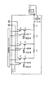
本実施形態においては、ガラス基板2上に2行2列(4個)の画素PE11、PE21、PE21及びPE22が設けられてセンサアレイ1が構成されているが、センサアレイ1を構成する画素の数はこれに限定されるものではない。各画素には、アモルファスシリコンを用いて形成されたPIN型フォトダイオードからなる光電変換素子PD及び光電変換素子PDが生成した信号電荷を蓄積する蓄積容量Csが設けられている。光電変換素子PD及び蓄積容量Csの一端は接地されており、他端は互いに接続されている。各画素には、更に、リセット用MOSトランジスタRT、選択用MOSトランジスタST及びソースフォロアMOSトランジスタ(読み出し用トランジスタ)FTが設けられている。リセット用MOSトランジスタRT、選択用MOSトランジスタST及びソースフォロアMOSトランジスタFTは、例えばアモルファスシリコン又はポリシリコンを用いて形成された薄膜トランジスタ(TFT)から構成されている。なお、蓄積容量Csは、光電変換素子PD自体に存在する容量の大きさが十分なものであれば設けられていなくてもよい。
In the present embodiment, the
画素PE11及びPE12のリセット用MOSトランジスタRTのゲートには、共通の共通リセット線R1が接続され、画素PE21及びPE22のリセット用MOSトランジスタRTのゲートには、共通の共通リセット線R2が接続されている。また、各リセット用MOSトランジスタRTの一端はリセット用電源5に接続され、他端は光電変換素子PD及び蓄積容量Csに接続されている。
A common common reset line R1 is connected to the gates of the reset MOS transistors RT of the pixels PE11 and PE12, and a common common reset line R2 is connected to the gates of the reset MOS transistors RT of the pixels PE21 and PE22. Yes. Further, one end of each reset MOS transistor RT is connected to the
画素PE11及びPE12の選択用MOSトランジスタSTのゲートには、共通の共通選択線S1が接続され、画素PE21及びPE22の選択用MOSトランジスタSTのゲートには、共通の共通選択線S2が接続されている。また、各選択用MOSトランジスタSTの一端はソースフォロア用電源(読み出し用電源)6に接続され、他端は当該画素内でソースフォロアMOSトランジスタFTのドレインに接続されている。 A common common selection line S1 is connected to the gates of the selection MOS transistors ST of the pixels PE11 and PE12, and a common common selection line S2 is connected to the gates of the selection MOS transistors ST of the pixels PE21 and PE22. Yes. One end of each selection MOS transistor ST is connected to a source follower power source (reading power source) 6 and the other end is connected to the drain of the source follower MOS transistor FT in the pixel.
画素PE11及びPE21のソースフォロアMOSトランジスタFTのソースには、共通の共通信号線Sig1が接続され、画素PE12及びPE22のソースフォロアMOSトランジスタFTのソースには、共通の共通信号線Sig2が接続されている。また、各ソースフォロアMOSトランジスタFTのゲートは、当該画素内で光電変換素子PD及び蓄積容量Csに接続されている。 A common common signal line Sig1 is connected to the sources of the source follower MOS transistors FT of the pixels PE11 and PE21, and a common common signal line Sig2 is connected to the sources of the source follower MOS transistors FT of the pixels PE12 and PE22. Yes. The gate of each source follower MOS transistor FT is connected to the photoelectric conversion element PD and the storage capacitor Cs in the pixel.
共通リセット線R1及びR2並びに共通選択線S1及びS2は、結晶シリコンを用いて形成されたシフトレジスタを備えた走査回路4に接続されている。また、共通信号線Sig1及びSig2は、結晶シリコンを用いて形成された読み出し回路3に接続されている。更に、共通信号線Sig1及びSig2には、ガラス基板2上に形成された定電流源Iが接続されている。読み出し回路3には、共通信号線Sig1及びSig2毎に、増幅器Amp1及びAmp2が設けられており、これらの出力信号を外部に順次出力するアナログマルチプレクサMUXも設けられている。また、センサアレイ1の受光面には、従来のものと同様に蛍光体層が設けられている。
The common reset lines R1 and R2 and the common selection lines S1 and S2 are connected to a
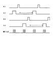
次に、第1の実施形態に係る光電変換装置(X線撮像装置)の動作について説明する。図2は、第1の実施形態に係る光電変換装置(X線撮像装置)の動作を示すタイミングチャートである。図2中のR1及びR2は、夫々共通リセット線R1、R2を介してリセット用MOSトランジスタRTのゲートに印加されるリセットパルスを示し、S1、S2は、夫々共通選択線S1、S2を介して選択用MOSトランジスタSTのゲートに印加される選択パルスを示し、MUX_CLKはアナログマルチプレクサMUXに印加されるパルスを示す。 Next, the operation of the photoelectric conversion apparatus (X-ray imaging apparatus) according to the first embodiment will be described. FIG. 2 is a timing chart showing the operation of the photoelectric conversion apparatus (X-ray imaging apparatus) according to the first embodiment. In FIG. 2, R1 and R2 indicate reset pulses applied to the gates of the reset MOS transistors RT via the common reset lines R1 and R2, respectively. S1 and S2 are indicated via the common selection lines S1 and S2, respectively. A selection pulse is applied to the gate of the selection MOS transistor ST, and MUX_CLK is a pulse applied to the analog multiplexer MUX.
放射線(X線)が光電変換装置に連続して照射されている状態で、走査回路4が共通リセット線R1にリセットパルスを印加すると、画素PE11及びPE12の光電変換素子PDの電位がリセットされた後、画素PE11及びPE12の光電変換素子PDが光電変換を開始し、蓄積容量Csに信号電荷が蓄積される。また、走査回路4が共通リセット線R2にリセットパルスを印加すると、画素PE21及びPE22の光電変換素子PDの電位がリセットされた後、画素PE21及びPE22の光電変換素子PDが光電変換を開始し、蓄積容量Csに信号電荷が蓄積される。
When the
そして、走査回路4が、共通リセット線R1にリセットパルスを印加した後に共通選択線S1に選択パルスを印加すると、光電変換素子PDのリセット以降、画素PE11及びPE12の蓄積容量Csに蓄積されていた信号電荷が信号線Sig1を介して読み出し回路3に読み出される。同様に、走査回路4が、共通リセット線R2にリセットパルスを印加した後に共通選択線S2に選択パルスを印加すると、光電変換素子PDのリセット以降、画素PE21及びPE22の蓄積容量Csに蓄積されていた信号電荷が信号線Sig2を介して読み出し回路3に読み出される。
When the
読み出し回路3は、パルスMUX_CLKに同期して、信号線Sig1及びSig2を介して出力されてきた信号を外部の処理装置等に出力する。
The
このような第1の実施形態では、全体的な回路の構成がソースフォロア回路となっている。従って、信号線Sig1及びSig2に寄生する寄生容量Pの影響を受けずに光電変換素子PDにより得られた信号を増幅して読み出すことができる。従って、大面積化に伴う出力の低下を回避することができる。このため、読み出し回路3内の増幅器Amp1及びAmp2自体で生じるノイズや外来ノイズの影響を受けにくいという効果も得られる。従って、高い感度を得ることもできる。更に、光電変換素子PDにより得られた信号がソースフォロアで増幅されており、また、読み出し回路3に定電流源が不要なので、読み出し回路3の構成は簡素であり、廉価な汎用の素子を用いて構成することが可能である。即ち、従来技術のように、特殊で消費電力の大きい低ノイズアンプや低電流源を要しない簡単な構成の読み出し回路を実現することができる。
In such a first embodiment, the overall circuit configuration is a source follower circuit. Therefore, the signal obtained by the photoelectric conversion element PD can be amplified and read without being affected by the parasitic capacitance P parasitic on the signal lines Sig1 and Sig2. Therefore, it is possible to avoid a decrease in output accompanying an increase in area. For this reason, the effect that it is hard to receive the influence of the noise which generate | occur | produces in amplifiers Amp1 and Amp2 itself in the
なお、上述の動作についての説明では、放射線(X線)を連続的に照射しているものとしているが、断続的に照射してもよい。また、X線撮像装置の構成に関し、選択用MOSトランジスタSTがソースフォロアMOSトランジスタFTのソース側に設けられていてもよい。また、定電流源の回路構成は、特に限定されるものではなく、例えば1又は2以上のTFTを組み合わせることにより構成することができる。 In the above description of the operation, radiation (X-rays) is continuously irradiated, but may be intermittently irradiated. Further, regarding the configuration of the X-ray imaging apparatus, the selection MOS transistor ST may be provided on the source side of the source follower MOS transistor FT. The circuit configuration of the constant current source is not particularly limited, and can be configured by combining, for example, one or two or more TFTs.
(第2の実施形態)
次に、本発明の第2の実施形態について説明する。図3は、本発明の第2の実施形態に係る光電変換装置、特にX線撮像装置の回路構成を示す回路図である。第2の実施形態では、第1の実施形態で用いられている定電流源Iの替わりに、アモルファスシリコンを用いて形成された薄膜トランジスタ(TFT)CTが設けられている。薄膜トランジスタCTのゲートには、定電流源用電源7から電圧が供給されている。このような構成では、定電流源を他のトランジスタ(リセット用、選択用、ソースフォロア用)等と同時に成膜して形成することができるため、簡易な製造プロセスで構成することができる。ここで、リセット用、選択用、ソースフォロア用、定電流源用の各薄膜トランジスタは積層する膜厚等を共通にしても良いし、又は個別の膜厚等にしても良い。また、不純物ドープの条件(n型又はp型)を共通にしても良いし、又は個別のドープ条件としても良い。更に、レーザーアニール等を用いて、一部をアモルファスシリコンで構成し、他の一部をポリシリコン化しても良い。
(Second Embodiment)
Next, a second embodiment of the present invention will be described. FIG. 3 is a circuit diagram showing a circuit configuration of a photoelectric conversion device, particularly an X-ray imaging device, according to the second embodiment of the present invention. In the second embodiment, instead of the constant current source I used in the first embodiment, a thin film transistor (TFT) CT formed using amorphous silicon is provided. A voltage is supplied from the constant current source power supply 7 to the gate of the thin film transistor CT. In such a configuration, the constant current source can be formed and formed simultaneously with other transistors (for reset, for selection, for source follower) and the like, so that it can be configured with a simple manufacturing process. Here, the reset, selection, source follower, and constant current source thin film transistors may have a common film thickness or the like, or may have individual film thicknesses. Further, the impurity doping conditions (n-type or p-type) may be common, or individual doping conditions may be used. Further, by using laser annealing or the like, one part may be made of amorphous silicon and the other part may be polysilicon.
なお、図3においては、薄膜トランジスタCT及び定電流源用電源7を備えた定電流源は、図11に示すように構成されている。この場合、定電流源を構成する薄膜トランジスタCTはn型、p型のいずれでも良い。 In FIG. 3, the constant current source including the thin film transistor CT and the constant current source power supply 7 is configured as shown in FIG. 11. In this case, the thin film transistor CT constituting the constant current source may be either n-type or p-type.
例えば、薄膜トランジスタCTがn型の薄膜トランジスタである場合、薄膜トランジスタCTは、ソース−ドレイン間電圧Vds、ソース−ドレイン間電流Ids、ゲート−ソース間電圧Vgs及びしきい値電圧Vthに関し、図4に示すようなVds−Ids特性を示す。従って、薄膜トランジスタCTのゲート電圧を制御して「Vds>Vgs−Vth」が満たされる飽和領域とすることにより、薄膜トランジスタCTを定電流源として用いることができる。 For example, when the thin film transistor CT is an n-type thin film transistor, the thin film transistor CT relates to the source-drain voltage Vds, the source-drain current Ids, the gate-source voltage Vgs, and the threshold voltage Vth as shown in FIG. Vds-Ids characteristics are shown. Accordingly, the thin film transistor CT can be used as a constant current source by controlling the gate voltage of the thin film transistor CT so that the saturation region satisfies “Vds> Vgs−Vth”.
更に、上式に従えば、薄膜トランジスタCTがn型の薄膜トランジスタである場合、図12に示すように、ゲートとソースとを互いに接続することにより、簡単な構成で定電流源を構成することもできる。また、必要な電流値によっては、図13に示すように、ゲートとソースとの間に抵抗を設けても良い。図12又は図13に示す構成によれば、定電流源用電源が不要となる。 Further, according to the above formula, when the thin film transistor CT is an n-type thin film transistor, the constant current source can be configured with a simple configuration by connecting the gate and the source to each other as shown in FIG. . Depending on the required current value, a resistor may be provided between the gate and the source as shown in FIG. The configuration shown in FIG. 12 or 13 eliminates the need for a constant current source.
更に、定電流源をガラス基板上に形成する場合の別の例を図14に示す。この例では擬似的な定電流源を、薄膜トランジスタなどを用いずに、ガラス基板上にパターニングされた抵抗で形成している。この場合の抵抗値は選択用MOSトランジスタSTのON抵抗値より十分大きいことが望ましい。 Furthermore, another example in the case of forming a constant current source on a glass substrate is shown in FIG. In this example, a pseudo constant current source is formed by a resistor patterned on a glass substrate without using a thin film transistor or the like. In this case, the resistance value is desirably sufficiently larger than the ON resistance value of the selection MOS transistor ST.
(第3の実施形態)
次に、本発明の第3の実施形態について説明する。図5は、本発明の第3の実施形態に係る光電変換装置、特にX線撮像装置の回路構成を示す回路図である。第2の実施形態では、定電流源を形成する薄膜トランジスタCTが画素と読み出し回路3との間に位置しているのに対し、第3の実施形態では、薄膜トランジスタCTが共通信号線上において、画素よりも読み出し回路3から離間して位置している。つまり、薄膜トランジスタCTと読み出し回路3との間に画素が位置している。
(Third embodiment)
Next, a third embodiment of the present invention will be described. FIG. 5 is a circuit diagram showing a circuit configuration of a photoelectric conversion device, particularly an X-ray imaging device, according to the third embodiment of the present invention. In the second embodiment, the thin film transistor CT forming the constant current source is positioned between the pixel and the
定電流源を読み出し回路から離間して設ける利点について、図15、図16、図17を用いて詳しく説明する。図15は各信号線に対して、定電流源を読み出し手段から離間して設けた場合の構成であり、図16は低電流源を読み出し手段側に設けた場合の構成である。図16のように定電流源を読み出し手段側に設けた場合、各ソースフォロアMOSトランジスタのソース電位Vsに対して、実際に読み出し手段で読み出される電圧Voutが信号線の抵抗成分R1、R2、R3の影響で低減する。たとえば画素Cを読み出す場合はΔV=I0×(R1+R2+R3)だけFT3のソース電位より低い電圧が読み出される。 The advantage of providing the constant current source away from the readout circuit will be described in detail with reference to FIGS. 15, 16, and 17. FIG. FIG. 15 shows a configuration when a constant current source is provided for each signal line apart from the reading means, and FIG. 16 shows a configuration when a low current source is provided on the reading means side. When the constant current source is provided on the reading means side as shown in FIG. 16, the voltage Vout actually read by the reading means with respect to the source potential Vs of each source follower MOS transistor is the resistance component R1, R2, R3 of the signal line. Reduced by the influence of For example, when pixel C is read, a voltage lower than the source potential of FT3 by ΔV = I0 × (R1 + R2 + R3) is read.
特に大面積の光電変換装置を形成するなど、信号線の抵抗が大きい場合には、この電圧降下は無視できない。図17に画素による電圧降下の様子を示す。一方、図15のように定電流源を読み出し手段と離間して設ける場合、上述の信号線抵抗による出力電圧降下を防ぐことができる。例えば画素Cを読み出す場合においても、電流はR1、R2、R3にはほとんど流れないため、ソースフォロアMOSトランジスタFT3のソース電圧を降下させることなく、読み出し手段で読み出すことが可能である。図17に、定電流源を読み出し手段から離間して設けた場合、電圧降下がほとんどないことを示す。図5及び図15に示すように、定電流源を読み出し手段から離間して設ける構成にすれば、大面積の光電変換装置のように信号線抵抗が無視できない場合にも、電圧降下などの不具合を生じることがない。 This voltage drop cannot be ignored particularly when the resistance of the signal line is large, such as when a photoelectric conversion device having a large area is formed. FIG. 17 shows a state of voltage drop by the pixel. On the other hand, when the constant current source is provided apart from the reading means as shown in FIG. 15, the output voltage drop due to the signal line resistance can be prevented. For example, even when the pixel C is read, since current hardly flows through R1, R2, and R3, it is possible to read by the reading means without lowering the source voltage of the source follower MOS transistor FT3. FIG. 17 shows that there is almost no voltage drop when the constant current source is provided apart from the reading means. As shown in FIGS. 5 and 15, if the constant current source is provided apart from the reading means, even if the signal line resistance cannot be ignored as in a large-area photoelectric conversion device, there is a problem such as a voltage drop. Will not occur.
本実施形態によれば、第1及び第2の実施形態で得られる効果に加えて、共通信号線に抵抗成分が存在しても、読み出し回路3が読み出す信号出力に対する抵抗成分による電圧降下を回避することができるという更なる効果が得られる。
According to this embodiment, in addition to the effects obtained in the first and second embodiments, a voltage drop due to the resistance component with respect to the signal output read by the
(第4の実施形態)
次に、本発明の第4の実施形態について説明する。図6は、本発明の第4の実施形態に係る光電変換装置、特にX線撮像装置の回路構成を示す回路図である。第4の実施形態においては、第3の実施形態に対し、共通信号線Sig1及びSig2に、読み出し走査用薄膜トランジスタ(TFT)RDTが設けられている。読み出し走査用薄膜トランジスタRDTは、ガラス基板2上の画素と読み出し回路3との間に形成されている。また、読み出し回路3には、アナログマルチプレクサMUXが設けられておらず、各信号線からの出力信号は単一の増幅器Ampに入力されるようになっている。更に、読み出し回路3には、読み出し走査用薄膜トランジスタRDTのゲート電圧を走査する読み出し走査回路8が設けられている。
(Fourth embodiment)
Next, a fourth embodiment of the present invention will be described. FIG. 6 is a circuit diagram showing a circuit configuration of a photoelectric conversion device, particularly an X-ray imaging device, according to the fourth embodiment of the present invention. In the fourth embodiment, a readout scanning thin film transistor (TFT) RDT is provided on the common signal lines Sig1 and Sig2 compared to the third embodiment. The readout scanning thin film transistor RDT is formed between the pixel on the
このように構成された第4の実施形態では、図7に示すように、第1の実施形態と同様にして蓄積容量Csに信号電荷が蓄積された後、信号線Sig1用のクロック信号CLK1及び信号線Sig2用のクロック信号CLK2に同期して読み出し走査用薄膜トランジスタRDTがオンとなり、蓄積されていた電荷が順次読み出し回路3により読み出される。
In the fourth embodiment configured as described above, as shown in FIG. 7, after the signal charge is stored in the storage capacitor Cs as in the first embodiment, the clock signal CLK1 for the signal line Sig1 and The readout scanning thin film transistor RDT is turned on in synchronization with the clock signal CLK2 for the signal line Sig2, and the accumulated charge is sequentially read out by the
このような第4の実施形態によれば、読み出し回路3に必要な増幅器の個数は1個であり、他にはロジック回路等は必要なだけである。即ち、読み出し回路3の構成がより一層簡素になっている。従って、ノイズがより一層低くなり、より簡単な構成でより高い感度を得ることができる。本実施形態において、レーザーアニール技術等を用いて走査用薄膜トランジスタRDTをポリシリコンで形成することは、走査速度の観点から望ましい。
According to the fourth embodiment as described above, the number of amplifiers required for the
(第5の実施形態)
次に、本発明の第5の実施形態について説明する。図8は、本発明の第5の実施形態に係る光電変換装置、特にX線撮像装置の回路構成を示す回路図である。第4の実施形態では、選択用MOSトランジスタSTがソースフォロアMOSトランジスタFTのドレインに接続されているのに対し、第5の実施形態では、選択用MOSトランジスタSTがソースフォロアMOSトランジスタFTのソースと信号線Sig1又はSig2との間に接続されている。ソースフォロアMOSトランジスタFTのドレインは、ソースフォロア用電源6に直接接続されている。
(Fifth embodiment)
Next, a fifth embodiment of the present invention will be described. FIG. 8 is a circuit diagram showing a circuit configuration of a photoelectric conversion apparatus, particularly an X-ray imaging apparatus, according to the fifth embodiment of the present invention. In the fourth embodiment, the selection MOS transistor ST is connected to the drain of the source follower MOS transistor FT, whereas in the fifth embodiment, the selection MOS transistor ST is connected to the source of the source follower MOS transistor FT. It is connected between the signal line Sig1 or Sig2. The drain of the source follower MOS transistor FT is directly connected to the source
このような第5の実施形態によっても、第4の実施形態と同様の効果が得られる。 According to the fifth embodiment, the same effect as that of the fourth embodiment can be obtained.
なお、X線の検出だけでなく、蛍光体層を設けずに可視光をそのまま受光するようにしてもよい。また、光電変換素子としては、PIN型フォトダイオードだけでなく、MIS型センサ等を用いてもよい。MIS型センサを用いる場合は、リセット用トランジスタに接続されたリセット用電源が図示しない制御手段により出力電圧を制御可能な構成としてもよい。 In addition to detecting X-rays, visible light may be received as it is without providing a phosphor layer. As the photoelectric conversion element, not only a PIN photodiode but also a MIS sensor or the like may be used. When the MIS type sensor is used, the reset power source connected to the reset transistor may be configured to control the output voltage by a control unit (not shown).
さらには光電変換素子としては、アモルファスセレン、ガリウム砒素、ヨウ化鉛、ヨウ化水銀など直接放射線(あるいはX線)を吸収して電荷を発生するいわゆる直接変換型素子を用いてもよい。この場合、アモルファスシリコンやポリシリコンで薄膜トランジスタを形成したガラス基板に、直接変換型素子を成膜あるいは接続して光電変換装置を構成することができる。 Furthermore, as the photoelectric conversion element, a so-called direct conversion type element that generates a charge by absorbing direct radiation (or X-rays) such as amorphous selenium, gallium arsenide, lead iodide, or mercury iodide may be used. In this case, a photoelectric conversion device can be configured by forming or connecting a direct conversion element on a glass substrate in which a thin film transistor is formed of amorphous silicon or polysilicon.
(第6の実施形態)
次に、本発明の第6の実施形態について説明する。第6の実施形態は、本発明の光電変換装置を用いたX線撮影システムの例である。図18は、本発明の第6の実施形態に係るX線撮影システムを示す図である。
(Sixth embodiment)
Next, a sixth embodiment of the present invention will be described. The sixth embodiment is an example of an X-ray imaging system using the photoelectric conversion device of the present invention. FIG. 18 is a diagram showing an X-ray imaging system according to the sixth embodiment of the present invention.
X線ルーム(撮影室)内において、X線チューブ(X線発生装置)6050で発生したX線6060は患者又は被験者6061の胸部6062を透過し、イメージセンサ6040に入射する。この入射したX線には患者6061の体の内部の情報が含まれている。X線の入射に対応してシンチレータ(蛍光体)は発光し、これをセンサーパネルの光電変換素子が光電変換して、電気的情報を得る。イメージセンサ6040は、この情報を電気信号(デジタル信号)としてイメージプロセッサ6070に出力する。画像処理手段としてのイメージプロセッサ6070は、受信した信号に対して画像処理を施して、コントロールルーム(操作室)の表示手段であるディスプレイ6080に出力する。ユーザは、ディスプレイ6080に表示された画像を観察して、患者6061の体の内部の情報を得ることができる。なお、イメージプロセッサ6070は、制御手段の機能も有しており、動画/静止画の撮影モードを切り換えたり、X線チューブ6050の制御を行ったりすることも可能である。
In the X-ray room (imaging room), the
また、イメージプロセッサ6070は、イメージセンサ6040から出力された電気信号を電話回線6090等の伝送処理手段を介して遠隔地へ転送し、ドクタールーム等の別の場所にある表示手段(ディスプレイ)6081に表示することもできる。また、イメージセンサ6040から出力された電気信号を光ディスク等の記録手段に保存し、この記録手段を用いて遠隔地の医師が診断することも可能である。また、記録手段となるフィルムプロセッサ6100によりフィルム6110に記録することもできる。
Further, the image processor 6070 transfers the electric signal output from the image sensor 6040 to a remote place via a transmission processing unit such as a
本X線撮影システムの特徴は、以下の点である。即ち、
(1)前述の光電変換装置が図中6040のイメージセンサ内部に設けられており、A/D変換されたデジタル出力はイメージプロセッサ6070で目的に応じた画像処理などが施される。
(2)イメージプロセッサ6070には図示しない制御手段が設けられており、制御手段はイメージセンサ6040、X線発生装置6050、ディスプレイ6080・6081、フィルムプロセッサ6100などを制御している。
The features of this X-ray imaging system are as follows. That is,
(1) The above-described photoelectric conversion device is provided in the image sensor 6040 in the drawing, and the A / D converted digital output is subjected to image processing or the like according to the purpose by an image processor 6070.
(2) The image processor 6070 is provided with control means (not shown), and the control means controls the image sensor 6040, the
1:センサアレイ
2:ガラス基板
3:読み出し回路
4:走査回路
5:リセット用電源
6:ソースフォロア用電源
7:定電流源用電源
8:読み出し走査回路
PE11、PE12、PE21、PE22:画素
PD:光電変換素子
Cs:蓄積容量
RT:リセット用MOSトランジスタ
ST:選択用MOSトランジスタ
FT:ソースフォロアMOSトランジスタ
CT:薄膜トランジスタ
RDT:読み出し走査用薄膜トランジスタ
Amp、Amp1、Amp2:増幅器
MUX:アナログマルチプレクサ
I:定電流源
R1、R2:共通リセット線
S1、S2:共通選択線
Sig1、Sig2:共通信号線
1: Sensor array 2: Glass substrate 3: Readout circuit 4: Scanning circuit 5: Power supply for reset 6: Power supply for source follower 7: Power supply for constant current source 8: Readout scanning circuit PE11, PE12, PE21, PE22: Pixel PD: Photoelectric conversion element Cs: Storage capacitor RT: Reset MOS transistor ST: Select MOS transistor FT: Source follower MOS transistor CT: Thin film transistor RDT: Read scan thin film transistor Amp, Amp1, Amp2: Amplifier MUX: Analog multiplexer I: Constant current source R1, R2: Common reset line S1, S2: Common selection line Sig1, Sig2: Common signal line
Claims (16)
前記光電変換素子にソースが接続され、ドレインにリセット用電源が接続されるリセット用トランジスタと、
前記光電変換素子にゲートが接続され、ドレインに読み出し用電源が接続される読み出し用トランジスタと、
前記読み出し用トランジスタのソースに接続された信号線と、
前記読み出し用電源又は前記信号線と前記読み出し用トランジスタとの間に接続された選択用トランジスタと、
前記信号線に接続された定電流源と、
を有することを特徴とする光電変換装置。 A photoelectric conversion element;
A reset transistor in which a source is connected to the photoelectric conversion element and a reset power source is connected to a drain;
A reading transistor having a gate connected to the photoelectric conversion element and a reading power supply connected to the drain;
A signal line connected to a source of the reading transistor;
A selection transistor connected between the readout power supply or the signal line and the readout transistor;
A constant current source connected to the signal line;
A photoelectric conversion device comprising:
前記定電流源は、前記読み出し用トランジスタよりも前記読み出し手段から離間した前記信号線上の位置に設けられていることを特徴とする請求項1又は2に記載の光電変換装置。 Read means connected to the signal line,
3. The photoelectric conversion device according to claim 1, wherein the constant current source is provided at a position on the signal line farther from the reading unit than the reading transistor.
前記光電変換素子にソースが接続され、ドレインにリセット用電源が接続されるリセット用トランジスタと、
前記光電変換素子にゲートが接続され、ドレインに読み出し用電源が接続される読み出し用トランジスタと、
前記読み出し用電源又は前記信号線と前記読み出し用トランジスタとの間に接続された選択用トランジスタと、
を備えた画素が2次元状に複数配列され、
前記複数の画素に接続された複数の共通信号線と、
前記共通信号線に接続された定電流源と、
を有することを特徴とする光電変換装置。 A photoelectric conversion element;
A reset transistor in which a source is connected to the photoelectric conversion element and a reset power source is connected to a drain;
A reading transistor having a gate connected to the photoelectric conversion element and a reading power supply connected to the drain;
A selection transistor connected between the readout power supply or the signal line and the readout transistor;
A plurality of pixels having a two-dimensional arrangement,
A plurality of common signal lines connected to the plurality of pixels;
A constant current source connected to the common signal line;
A photoelectric conversion device comprising:
前記制御手段は、X線発生装置および光電変換装置の動作を制御することにより、
被写体を透過したX線画像を読み取ることを特徴とするX線撮影システム。 The photoelectric conversion device according to claim 1, an X-ray generation device, and a control unit,
The control means controls the operations of the X-ray generator and the photoelectric conversion device,
An X-ray imaging system that reads an X-ray image transmitted through a subject.
Priority Applications (7)
| Application Number | Priority Date | Filing Date | Title |
|---|---|---|---|
| JP2004180899A JP2005175418A (en) | 2003-11-19 | 2004-06-18 | Photoelectric conversion apparatus |
| RU2006121485/09A RU2345502C2 (en) | 2003-11-19 | 2004-11-10 | Photovoltaic conversion device |
| US10/540,423 US7592599B2 (en) | 2003-11-19 | 2004-11-10 | Photoelectric converting apparatus |
| EP04799719A EP1687972A4 (en) | 2003-11-19 | 2004-11-10 | Photoelectric converting apparatus |
| PCT/JP2004/017042 WO2005050982A1 (en) | 2003-11-19 | 2004-11-10 | Photoelectric converting apparatus |
| TW093134976A TW200521607A (en) | 2003-11-19 | 2004-11-15 | Photoelectric converting apparatus |
| US12/544,938 US7923696B2 (en) | 2003-11-19 | 2009-08-20 | Photoelectric converting apparatus |
Applications Claiming Priority (2)
| Application Number | Priority Date | Filing Date | Title |
|---|---|---|---|
| JP2003389274 | 2003-11-19 | ||
| JP2004180899A JP2005175418A (en) | 2003-11-19 | 2004-06-18 | Photoelectric conversion apparatus |
Publications (2)
| Publication Number | Publication Date |
|---|---|
| JP2005175418A true JP2005175418A (en) | 2005-06-30 |
| JP2005175418A5 JP2005175418A5 (en) | 2007-07-19 |
Family
ID=34622175
Family Applications (1)
| Application Number | Title | Priority Date | Filing Date |
|---|---|---|---|
| JP2004180899A Pending JP2005175418A (en) | 2003-11-19 | 2004-06-18 | Photoelectric conversion apparatus |
Country Status (6)
| Country | Link |
|---|---|
| US (2) | US7592599B2 (en) |
| EP (1) | EP1687972A4 (en) |
| JP (1) | JP2005175418A (en) |
| RU (1) | RU2345502C2 (en) |
| TW (1) | TW200521607A (en) |
| WO (1) | WO2005050982A1 (en) |
Cited By (6)
| Publication number | Priority date | Publication date | Assignee | Title |
|---|---|---|---|---|
| JP2007035773A (en) * | 2005-07-25 | 2007-02-08 | Canon Inc | Electromagnetic wave detector, radiation detector, and radiation imaging system |
| JP2007289281A (en) * | 2006-04-21 | 2007-11-08 | Canon Inc | Radioimaging apparatus |
| JP2008282844A (en) * | 2007-05-08 | 2008-11-20 | Mitsubishi Electric Corp | Photosensor and manufacturing method thereof |
| JP2010004026A (en) * | 2008-05-22 | 2010-01-07 | Semiconductor Energy Lab Co Ltd | Photoelectric conversion device, and electronic apparatus provided with the photoelectric conversion device |
| WO2011111529A1 (en) * | 2010-03-12 | 2011-09-15 | Semiconductor Energy Laboratory Co., Ltd. | Semiconductor device |
| US9450002B2 (en) | 2012-10-09 | 2016-09-20 | Canon Kabushiki Kaisha | Detecting apparatus and detecting system |
Families Citing this family (38)
| Publication number | Priority date | Publication date | Assignee | Title |
|---|---|---|---|---|
| JP2005175418A (en) | 2003-11-19 | 2005-06-30 | Canon Inc | Photoelectric conversion apparatus |
| JP4441294B2 (en) * | 2004-03-12 | 2010-03-31 | キヤノン株式会社 | Radiation imaging apparatus and control method thereof |
| JP4469638B2 (en) | 2004-03-12 | 2010-05-26 | キヤノン株式会社 | Reading device and image photographing device |
| JP2005287773A (en) | 2004-03-31 | 2005-10-20 | Canon Inc | Image photography apparatus and image photography system |
| JP4307322B2 (en) * | 2004-05-18 | 2009-08-05 | キヤノン株式会社 | Radiation imaging apparatus and radiation imaging system |
| JP5058517B2 (en) | 2005-06-14 | 2012-10-24 | キヤノン株式会社 | Radiation imaging apparatus, control method therefor, and radiation imaging system |
| JP4965931B2 (en) * | 2005-08-17 | 2012-07-04 | キヤノン株式会社 | Radiation imaging apparatus, radiation imaging system, control method thereof, and control program |
| JP4750512B2 (en) | 2005-09-01 | 2011-08-17 | キヤノン株式会社 | Radiation imaging apparatus, control method therefor, and radiation imaging system |
| JP5317388B2 (en) * | 2005-09-30 | 2013-10-16 | キヤノン株式会社 | Radiation imaging apparatus, radiation imaging system, and program |
| JP2007104219A (en) | 2005-10-03 | 2007-04-19 | Canon Inc | Radiation photography instrument and its control method, radiation photography system |
| US7256605B2 (en) * | 2005-11-14 | 2007-08-14 | Semiconductor Components Industries, L.L.C. | Diagnostic circuit and method therefor |
| JP4834518B2 (en) | 2005-11-29 | 2011-12-14 | キヤノン株式会社 | Radiation imaging apparatus, control method therefor, and recording medium on which program for executing the same is recorded |
| JP2007151761A (en) * | 2005-12-02 | 2007-06-21 | Canon Inc | Apparatus, system, method, and program for radiation imaging |
| JP4989197B2 (en) * | 2005-12-13 | 2012-08-01 | キヤノン株式会社 | Radiation imaging apparatus, radiation imaging system, and correction method |
| JP4891096B2 (en) * | 2006-01-30 | 2012-03-07 | キヤノン株式会社 | Radiation imaging device |
| JP5043448B2 (en) * | 2006-03-10 | 2012-10-10 | キヤノン株式会社 | Radiation imaging apparatus and radiation imaging system |
| JP4850730B2 (en) * | 2006-03-16 | 2012-01-11 | キヤノン株式会社 | Imaging apparatus, processing method thereof, and program |
| JP4847202B2 (en) * | 2006-04-27 | 2011-12-28 | キヤノン株式会社 | Imaging apparatus and radiation imaging system |
| JP4989120B2 (en) * | 2006-06-16 | 2012-08-01 | キヤノン株式会社 | Radiation imaging system and driving method thereof |
| JP5159161B2 (en) * | 2006-06-26 | 2013-03-06 | キヤノン株式会社 | Radiation imaging apparatus, radiation imaging system and control method thereof |
| JP5038031B2 (en) | 2006-07-11 | 2012-10-03 | キヤノン株式会社 | Radiography apparatus, driving method thereof and radiation imaging system |
| JP2008042478A (en) * | 2006-08-04 | 2008-02-21 | Canon Inc | Imaging device, radiation ray imaging device and its driving method |
| JP5300216B2 (en) * | 2006-08-29 | 2013-09-25 | キヤノン株式会社 | Electronic cassette type radiation detector |
| JP4986771B2 (en) * | 2006-08-31 | 2012-07-25 | キヤノン株式会社 | Imaging apparatus, driving method thereof, and radiation imaging system |
| US7869568B2 (en) * | 2007-03-13 | 2011-01-11 | Canon Kabushiki Kaisha | Radiation imaging apparatus, and method and program for controlling radiation imaging apparatus |
| JP2009141439A (en) * | 2007-12-03 | 2009-06-25 | Canon Inc | Radiation imaging apparatus, driving method thereof, and program |
| JP5274098B2 (en) | 2008-04-30 | 2013-08-28 | キヤノン株式会社 | Imaging apparatus, radiation imaging system, control method thereof, and program |
| JP4759590B2 (en) * | 2008-05-09 | 2011-08-31 | キヤノン株式会社 | Photoelectric conversion device and imaging system using the same |
| JP2010005212A (en) * | 2008-06-27 | 2010-01-14 | Canon Inc | Radiographic imaging apparatus, control method thereof and radiographic imaging system |
| JP4785963B2 (en) * | 2009-10-09 | 2011-10-05 | キヤノン株式会社 | Solid-state imaging device |
| JP5717329B2 (en) * | 2009-10-09 | 2015-05-13 | キヤノン株式会社 | Solid-state imaging device and manufacturing method thereof |
| GB0920684D0 (en) * | 2009-11-26 | 2010-01-13 | Plastic Logic Ltd | Display systems |
| JP2012129425A (en) * | 2010-12-16 | 2012-07-05 | Canon Inc | Matrix substrate, detection apparatus, detection system and detection apparatus driving method |
| JP5986524B2 (en) | 2013-02-28 | 2016-09-06 | キヤノン株式会社 | Radiation imaging apparatus and radiation imaging system |
| JP6016673B2 (en) | 2013-02-28 | 2016-10-26 | キヤノン株式会社 | Radiation imaging apparatus and radiation imaging system |
| JP5934128B2 (en) | 2013-02-28 | 2016-06-15 | キヤノン株式会社 | Radiation imaging apparatus and radiation imaging system |
| JP6587517B2 (en) | 2015-11-13 | 2019-10-09 | キヤノン株式会社 | Radiation imaging system |
| US11656124B1 (en) * | 2022-01-26 | 2023-05-23 | Innolux Corporation | Sensing device |
Citations (12)
| Publication number | Priority date | Publication date | Assignee | Title |
|---|---|---|---|---|
| JPH0513686A (en) * | 1991-07-08 | 1993-01-22 | Sumitomo Electric Ind Ltd | Semiconductor constant current source circuit |
| JPH0513687A (en) * | 1991-07-08 | 1993-01-22 | Sumitomo Electric Ind Ltd | Semiconductor constant current source circuit |
| JPH09252434A (en) * | 1996-03-14 | 1997-09-22 | Toshiba Corp | Solid-state image pickup device |
| JPH10108075A (en) * | 1996-09-27 | 1998-04-24 | Toshiba Corp | Signal amplification type image-pickup device |
| JP2001251555A (en) * | 2000-03-02 | 2001-09-14 | Canon Inc | Solid-state image pickup device |
| JP2001298663A (en) * | 2000-04-12 | 2001-10-26 | Semiconductor Energy Lab Co Ltd | Semiconductor device and its drive method |
| JP2001308306A (en) * | 2000-04-21 | 2001-11-02 | Semiconductor Energy Lab Co Ltd | Semiconductor device and its driving method |
| JP2002148342A (en) * | 2000-11-07 | 2002-05-22 | Canon Inc | Radiation imaging device |
| JP2002251164A (en) * | 2000-09-14 | 2002-09-06 | Semiconductor Energy Lab Co Ltd | Area sensor and display device |
| JP2003092396A (en) * | 2001-09-17 | 2003-03-28 | Sony Corp | Solid-state image pickup device and method for manufacturing the same |
| JP2003322681A (en) * | 2002-05-07 | 2003-11-14 | Toshiba Corp | X-ray detector and x-ray diagnosis system |
| JP2003322682A (en) * | 2002-05-07 | 2003-11-14 | Toshiba Corp | X-ray detector |
Family Cites Families (21)
| Publication number | Priority date | Publication date | Assignee | Title |
|---|---|---|---|---|
| US6903771B2 (en) * | 2000-03-02 | 2005-06-07 | Canon Kabushiki Kaisha | Image pickup apparatus |
| JP3788561B2 (en) | 1999-05-13 | 2006-06-21 | シャープ株式会社 | Solid-state imaging device |
| JP2001251557A (en) * | 1999-12-27 | 2001-09-14 | Canon Inc | Area sensor, image input device having the same and method for driving the area sensor |
| WO2001057554A2 (en) * | 2000-02-02 | 2001-08-09 | Koninklijke Philips Electronics N.V. | Sensor and method of operating the sensor |
| US6965408B2 (en) * | 2000-02-28 | 2005-11-15 | Canon Kabushiki Kaisha | Solid-state image pickup device having a photoelectric conversion unit and a punch-through current suppression circuit |
| JP4441042B2 (en) | 2000-03-09 | 2010-03-31 | キヤノン株式会社 | Solid-state imaging device |
| US6855937B2 (en) * | 2001-05-18 | 2005-02-15 | Canon Kabushiki Kaisha | Image pickup apparatus |
| US6952015B2 (en) * | 2001-07-30 | 2005-10-04 | Canon Kabushiki Kaisha | Image pick-up apparatus and image pick-up system |
| JP3951879B2 (en) * | 2002-10-04 | 2007-08-01 | ソニー株式会社 | Solid-state imaging device and driving method thereof |
| JP4412911B2 (en) | 2003-03-28 | 2010-02-10 | 西松建設株式会社 | Water pollution control system and pollution control method |
| JP2005175418A (en) | 2003-11-19 | 2005-06-30 | Canon Inc | Photoelectric conversion apparatus |
| JP4533010B2 (en) * | 2003-11-20 | 2010-08-25 | キヤノン株式会社 | Radiation imaging apparatus, radiation imaging method, and radiation imaging system |
| JP4469638B2 (en) * | 2004-03-12 | 2010-05-26 | キヤノン株式会社 | Reading device and image photographing device |
| JP4441294B2 (en) * | 2004-03-12 | 2010-03-31 | キヤノン株式会社 | Radiation imaging apparatus and control method thereof |
| JP4074599B2 (en) * | 2004-03-26 | 2008-04-09 | シャープ株式会社 | Amplification type solid-state imaging device |
| US7403594B2 (en) * | 2004-03-31 | 2008-07-22 | Canon Kabushiki Kaisha | Radiation imaging apparatus and control method therefor |
| JP2005287773A (en) * | 2004-03-31 | 2005-10-20 | Canon Inc | Image photography apparatus and image photography system |
| JP4307322B2 (en) * | 2004-05-18 | 2009-08-05 | キヤノン株式会社 | Radiation imaging apparatus and radiation imaging system |
| JP5058517B2 (en) * | 2005-06-14 | 2012-10-24 | キヤノン株式会社 | Radiation imaging apparatus, control method therefor, and radiation imaging system |
| JP4965931B2 (en) * | 2005-08-17 | 2012-07-04 | キヤノン株式会社 | Radiation imaging apparatus, radiation imaging system, control method thereof, and control program |
| JP4750512B2 (en) * | 2005-09-01 | 2011-08-17 | キヤノン株式会社 | Radiation imaging apparatus, control method therefor, and radiation imaging system |
-
2004
- 2004-06-18 JP JP2004180899A patent/JP2005175418A/en active Pending
- 2004-11-10 WO PCT/JP2004/017042 patent/WO2005050982A1/en active Application Filing
- 2004-11-10 RU RU2006121485/09A patent/RU2345502C2/en not_active IP Right Cessation
- 2004-11-10 US US10/540,423 patent/US7592599B2/en not_active Expired - Fee Related
- 2004-11-10 EP EP04799719A patent/EP1687972A4/en not_active Withdrawn
- 2004-11-15 TW TW093134976A patent/TW200521607A/en unknown
-
2009
- 2009-08-20 US US12/544,938 patent/US7923696B2/en not_active Expired - Fee Related
Patent Citations (12)
| Publication number | Priority date | Publication date | Assignee | Title |
|---|---|---|---|---|
| JPH0513686A (en) * | 1991-07-08 | 1993-01-22 | Sumitomo Electric Ind Ltd | Semiconductor constant current source circuit |
| JPH0513687A (en) * | 1991-07-08 | 1993-01-22 | Sumitomo Electric Ind Ltd | Semiconductor constant current source circuit |
| JPH09252434A (en) * | 1996-03-14 | 1997-09-22 | Toshiba Corp | Solid-state image pickup device |
| JPH10108075A (en) * | 1996-09-27 | 1998-04-24 | Toshiba Corp | Signal amplification type image-pickup device |
| JP2001251555A (en) * | 2000-03-02 | 2001-09-14 | Canon Inc | Solid-state image pickup device |
| JP2001298663A (en) * | 2000-04-12 | 2001-10-26 | Semiconductor Energy Lab Co Ltd | Semiconductor device and its drive method |
| JP2001308306A (en) * | 2000-04-21 | 2001-11-02 | Semiconductor Energy Lab Co Ltd | Semiconductor device and its driving method |
| JP2002251164A (en) * | 2000-09-14 | 2002-09-06 | Semiconductor Energy Lab Co Ltd | Area sensor and display device |
| JP2002148342A (en) * | 2000-11-07 | 2002-05-22 | Canon Inc | Radiation imaging device |
| JP2003092396A (en) * | 2001-09-17 | 2003-03-28 | Sony Corp | Solid-state image pickup device and method for manufacturing the same |
| JP2003322681A (en) * | 2002-05-07 | 2003-11-14 | Toshiba Corp | X-ray detector and x-ray diagnosis system |
| JP2003322682A (en) * | 2002-05-07 | 2003-11-14 | Toshiba Corp | X-ray detector |
Cited By (13)
| Publication number | Priority date | Publication date | Assignee | Title |
|---|---|---|---|---|
| US8164065B2 (en) | 2005-07-25 | 2012-04-24 | Canon Kabushiki Kaisha | Radiation detecting apparatus, and radiation image pickup system |
| JP2007035773A (en) * | 2005-07-25 | 2007-02-08 | Canon Inc | Electromagnetic wave detector, radiation detector, and radiation imaging system |
| JP2007289281A (en) * | 2006-04-21 | 2007-11-08 | Canon Inc | Radioimaging apparatus |
| JP2008282844A (en) * | 2007-05-08 | 2008-11-20 | Mitsubishi Electric Corp | Photosensor and manufacturing method thereof |
| JP2010004026A (en) * | 2008-05-22 | 2010-01-07 | Semiconductor Energy Lab Co Ltd | Photoelectric conversion device, and electronic apparatus provided with the photoelectric conversion device |
| JP2014017522A (en) * | 2008-05-22 | 2014-01-30 | Semiconductor Energy Lab Co Ltd | Electronic apparatus |
| JP2011211182A (en) * | 2010-03-12 | 2011-10-20 | Semiconductor Energy Lab Co Ltd | Semiconductor device |
| WO2011111529A1 (en) * | 2010-03-12 | 2011-09-15 | Semiconductor Energy Laboratory Co., Ltd. | Semiconductor device |
| JP2012256914A (en) * | 2010-03-12 | 2012-12-27 | Semiconductor Energy Lab Co Ltd | Semiconductor device |
| US8766338B2 (en) | 2010-03-12 | 2014-07-01 | Semiconductor Energy Laboratory Co., Ltd. | Semiconductor device including photosensor and transistor having oxide semiconductor |
| US9066035B2 (en) | 2010-03-12 | 2015-06-23 | Semiconductor Energy Laboratory Co., Ltd. | Semiconductor device including photosensor and transistor having oxide semiconductor active layer |
| US9985069B2 (en) | 2010-03-12 | 2018-05-29 | Semiconductor Energy Laboratory Co., Ltd. | Semiconductor device |
| US9450002B2 (en) | 2012-10-09 | 2016-09-20 | Canon Kabushiki Kaisha | Detecting apparatus and detecting system |
Also Published As
| Publication number | Publication date |
|---|---|
| US7592599B2 (en) | 2009-09-22 |
| WO2005050982A1 (en) | 2005-06-02 |
| TW200521607A (en) | 2005-07-01 |
| RU2006121485A (en) | 2007-12-27 |
| EP1687972A4 (en) | 2013-01-16 |
| US20090309035A1 (en) | 2009-12-17 |
| US20060119719A1 (en) | 2006-06-08 |
| RU2345502C2 (en) | 2009-01-27 |
| EP1687972A1 (en) | 2006-08-09 |
| US7923696B2 (en) | 2011-04-12 |
Similar Documents
| Publication | Publication Date | Title |
|---|---|---|
| JP2005175418A (en) | Photoelectric conversion apparatus | |
| JP4307230B2 (en) | Radiation imaging apparatus and radiation imaging method | |
| JP4307322B2 (en) | Radiation imaging apparatus and radiation imaging system | |
| EP1848198B1 (en) | Imaging apparartus and radiation imaging system | |
| JP4991459B2 (en) | Imaging apparatus and radiation imaging system | |
| JP3066944B2 (en) | Photoelectric conversion device, driving method thereof, and system having the same | |
| JP6057511B2 (en) | Imaging apparatus and radiation imaging system | |
| JP4750512B2 (en) | Radiation imaging apparatus, control method therefor, and radiation imaging system | |
| US20130342514A1 (en) | Detection apparatus, detection system, and detection apparatus drive method | |
| JP5171431B2 (en) | Photoelectric conversion device, radiation imaging device, and radiation detection device | |
| US20130299678A1 (en) | Solid-state imaging apparatus and imaging system | |
| JP2007050053A (en) | Radiographic equipment, its control method and radiographic system | |
| JP2005253783A (en) | Reader and image photography device | |
| JP4383899B2 (en) | Radiation imaging apparatus and radiation imaging system | |
| JP4343893B2 (en) | Photoelectric conversion device, radiation reading device, and driving method of photoelectric conversion device | |
| CN100579451C (en) | Imaging apparatus, radiation imaging apparatus, and radiation imaging system | |
| CN100452842C (en) | Photoelectric converting apparatus | |
| JP2002051262A (en) | Image pickup device, radiograph pickup device and radiograph pickup system using the same | |
| JP2013033945A (en) | Detection device and detection system | |
| JP2006186032A (en) | Radiation imager | |
| JP2012134827A (en) | Radiation image detector | |
| JP2007005938A (en) | Photoelectric converter and drive method thereof |
Legal Events
| Date | Code | Title | Description |
|---|---|---|---|
| A521 | Request for written amendment filed |
Free format text: JAPANESE INTERMEDIATE CODE: A523 Effective date: 20070606 |
|
| A621 | Written request for application examination |
Free format text: JAPANESE INTERMEDIATE CODE: A621 Effective date: 20070606 |
|
| A131 | Notification of reasons for refusal |
Free format text: JAPANESE INTERMEDIATE CODE: A131 Effective date: 20110705 |
|
| A521 | Request for written amendment filed |
Free format text: JAPANESE INTERMEDIATE CODE: A523 Effective date: 20110829 |
|
| A02 | Decision of refusal |
Free format text: JAPANESE INTERMEDIATE CODE: A02 Effective date: 20120605 |