JP4305354B2 - 半導体装置およびその製造方法 - Google Patents
半導体装置およびその製造方法 Download PDFInfo
- Publication number
- JP4305354B2 JP4305354B2 JP2004290133A JP2004290133A JP4305354B2 JP 4305354 B2 JP4305354 B2 JP 4305354B2 JP 2004290133 A JP2004290133 A JP 2004290133A JP 2004290133 A JP2004290133 A JP 2004290133A JP 4305354 B2 JP4305354 B2 JP 4305354B2
- Authority
- JP
- Japan
- Prior art keywords
- electrode layer
- film
- organic resin
- resin film
- layer
- Prior art date
- Legal status (The legal status is an assumption and is not a legal conclusion. Google has not performed a legal analysis and makes no representation as to the accuracy of the status listed.)
- Expired - Fee Related
Links
Images


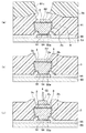


Classifications
-
- H—ELECTRICITY
- H10—SEMICONDUCTOR DEVICES; ELECTRIC SOLID-STATE DEVICES NOT OTHERWISE PROVIDED FOR
- H10W—GENERIC PACKAGES, INTERCONNECTIONS, CONNECTORS OR OTHER CONSTRUCTIONAL DETAILS OF DEVICES COVERED BY CLASS H10
- H10W72/00—Interconnections or connectors in packages
- H10W72/01—Manufacture or treatment
- H10W72/019—Manufacture or treatment of bond pads
-
- H—ELECTRICITY
- H10—SEMICONDUCTOR DEVICES; ELECTRIC SOLID-STATE DEVICES NOT OTHERWISE PROVIDED FOR
- H10W—GENERIC PACKAGES, INTERCONNECTIONS, CONNECTORS OR OTHER CONSTRUCTIONAL DETAILS OF DEVICES COVERED BY CLASS H10
- H10W72/00—Interconnections or connectors in packages
- H10W72/90—Bond pads, in general
-
- H—ELECTRICITY
- H10—SEMICONDUCTOR DEVICES; ELECTRIC SOLID-STATE DEVICES NOT OTHERWISE PROVIDED FOR
- H10W—GENERIC PACKAGES, INTERCONNECTIONS, CONNECTORS OR OTHER CONSTRUCTIONAL DETAILS OF DEVICES COVERED BY CLASS H10
- H10W72/00—Interconnections or connectors in packages
- H10W72/50—Bond wires
- H10W72/531—Shapes of wire connectors
- H10W72/536—Shapes of wire connectors the connected ends being ball-shaped
-
- H—ELECTRICITY
- H10—SEMICONDUCTOR DEVICES; ELECTRIC SOLID-STATE DEVICES NOT OTHERWISE PROVIDED FOR
- H10W—GENERIC PACKAGES, INTERCONNECTIONS, CONNECTORS OR OTHER CONSTRUCTIONAL DETAILS OF DEVICES COVERED BY CLASS H10
- H10W72/00—Interconnections or connectors in packages
- H10W72/50—Bond wires
- H10W72/551—Materials of bond wires
- H10W72/552—Materials of bond wires comprising metals or metalloids, e.g. silver
- H10W72/5522—Materials of bond wires comprising metals or metalloids, e.g. silver comprising gold [Au]
-
- H—ELECTRICITY
- H10—SEMICONDUCTOR DEVICES; ELECTRIC SOLID-STATE DEVICES NOT OTHERWISE PROVIDED FOR
- H10W—GENERIC PACKAGES, INTERCONNECTIONS, CONNECTORS OR OTHER CONSTRUCTIONAL DETAILS OF DEVICES COVERED BY CLASS H10
- H10W72/00—Interconnections or connectors in packages
- H10W72/50—Bond wires
- H10W72/551—Materials of bond wires
- H10W72/552—Materials of bond wires comprising metals or metalloids, e.g. silver
- H10W72/5524—Materials of bond wires comprising metals or metalloids, e.g. silver comprising aluminium [Al]
-
- H—ELECTRICITY
- H10—SEMICONDUCTOR DEVICES; ELECTRIC SOLID-STATE DEVICES NOT OTHERWISE PROVIDED FOR
- H10W—GENERIC PACKAGES, INTERCONNECTIONS, CONNECTORS OR OTHER CONSTRUCTIONAL DETAILS OF DEVICES COVERED BY CLASS H10
- H10W72/00—Interconnections or connectors in packages
- H10W72/50—Bond wires
- H10W72/59—Bond pads specially adapted therefor
-
- H—ELECTRICITY
- H10—SEMICONDUCTOR DEVICES; ELECTRIC SOLID-STATE DEVICES NOT OTHERWISE PROVIDED FOR
- H10W—GENERIC PACKAGES, INTERCONNECTIONS, CONNECTORS OR OTHER CONSTRUCTIONAL DETAILS OF DEVICES COVERED BY CLASS H10
- H10W72/00—Interconnections or connectors in packages
- H10W72/90—Bond pads, in general
- H10W72/981—Auxiliary members, e.g. spacers
- H10W72/983—Reinforcing structures, e.g. collars
-
- H—ELECTRICITY
- H10—SEMICONDUCTOR DEVICES; ELECTRIC SOLID-STATE DEVICES NOT OTHERWISE PROVIDED FOR
- H10W—GENERIC PACKAGES, INTERCONNECTIONS, CONNECTORS OR OTHER CONSTRUCTIONAL DETAILS OF DEVICES COVERED BY CLASS H10
- H10W74/00—Encapsulations, e.g. protective coatings
Landscapes
- Internal Circuitry In Semiconductor Integrated Circuit Devices (AREA)
- Wire Bonding (AREA)
Priority Applications (1)
| Application Number | Priority Date | Filing Date | Title |
|---|---|---|---|
| JP2004290133A JP4305354B2 (ja) | 2004-10-01 | 2004-10-01 | 半導体装置およびその製造方法 |
Applications Claiming Priority (1)
| Application Number | Priority Date | Filing Date | Title |
|---|---|---|---|
| JP2004290133A JP4305354B2 (ja) | 2004-10-01 | 2004-10-01 | 半導体装置およびその製造方法 |
Publications (3)
| Publication Number | Publication Date |
|---|---|
| JP2006108234A JP2006108234A (ja) | 2006-04-20 |
| JP2006108234A5 JP2006108234A5 (cg-RX-API-DMAC7.html) | 2009-01-29 |
| JP4305354B2 true JP4305354B2 (ja) | 2009-07-29 |
Family
ID=36377626
Family Applications (1)
| Application Number | Title | Priority Date | Filing Date |
|---|---|---|---|
| JP2004290133A Expired - Fee Related JP4305354B2 (ja) | 2004-10-01 | 2004-10-01 | 半導体装置およびその製造方法 |
Country Status (1)
| Country | Link |
|---|---|
| JP (1) | JP4305354B2 (cg-RX-API-DMAC7.html) |
Families Citing this family (6)
| Publication number | Priority date | Publication date | Assignee | Title |
|---|---|---|---|---|
| JP2008066450A (ja) * | 2006-09-06 | 2008-03-21 | Rohm Co Ltd | 半導体装置 |
| JP2008091454A (ja) * | 2006-09-29 | 2008-04-17 | Rohm Co Ltd | 半導体装置及び半導体装置の製造方法 |
| JP2011258871A (ja) * | 2010-06-11 | 2011-12-22 | Fujitsu Ltd | 回路基板及びその製造方法 |
| JP6080961B2 (ja) * | 2013-09-05 | 2017-02-15 | 三菱電機株式会社 | 半導体装置およびその製造方法 |
| JP2016174021A (ja) | 2015-03-16 | 2016-09-29 | 株式会社東芝 | 半導体装置 |
| JP6607771B2 (ja) * | 2015-12-03 | 2019-11-20 | ローム株式会社 | 半導体装置 |
-
2004
- 2004-10-01 JP JP2004290133A patent/JP4305354B2/ja not_active Expired - Fee Related
Also Published As
| Publication number | Publication date |
|---|---|
| JP2006108234A (ja) | 2006-04-20 |
Similar Documents
| Publication | Publication Date | Title |
|---|---|---|
| JP3482779B2 (ja) | 半導体装置およびその製造方法 | |
| KR100419813B1 (ko) | 반도체 장치 및 그 제조 방법 | |
| US9425147B2 (en) | Semiconductor device | |
| JP6014354B2 (ja) | 半導体装置の製造方法 | |
| US9922928B2 (en) | Semiconductor device and method of manufacturing semiconductor device | |
| US7800239B2 (en) | Thick metal interconnect with metal pad caps at selective sites and process for making the same | |
| US6720204B2 (en) | Method of using hydrogen plasma to pre-clean copper surfaces during Cu/Cu or Cu/metal bonding | |
| CN103296007B (zh) | 用于传导垫的保护层及其形成方法 | |
| US20100164105A1 (en) | Semiconductor device and method of manufacturing the same | |
| WO2010125682A1 (ja) | 半導体装置およびその製造方法 | |
| JP2007042817A (ja) | 絶縁ゲート型半導体装置およびその製造方法 | |
| JP2000340569A (ja) | 半導体装置の配線構造及びその形成方法 | |
| US6400026B1 (en) | Semiconductor device with the copper containing aluminum alloy bond pad on an active region | |
| US10790226B2 (en) | Integrated electronic device with a redistribution region and a high resilience to mechanical stresses and method for its preparation | |
| JP2006108234A (ja) | 半導体装置およびその製造方法 | |
| JP2005183866A (ja) | 半導体ウェーハ及びダイシング方法 | |
| JP4639138B2 (ja) | 半導体装置 | |
| US10892239B1 (en) | Bond pad reliability of semiconductor devices | |
| JP4293103B2 (ja) | 半導体装置の製造方法 | |
| JP2006108235A (ja) | 半導体装置およびその製造方法 | |
| JP2011018832A (ja) | 半導体装置及びその製造方法 | |
| JP2004221098A (ja) | 半導体装置およびその製造方法 | |
| US11501979B1 (en) | Semiconductor device and method of producing a semiconductor device | |
| JP2003347338A (ja) | 半導体装置 | |
| JP2006203025A (ja) | 半導体装置及びその製造方法 |
Legal Events
| Date | Code | Title | Description |
|---|---|---|---|
| A621 | Written request for application examination |
Free format text: JAPANESE INTERMEDIATE CODE: A621 Effective date: 20061129 |
|
| A977 | Report on retrieval |
Free format text: JAPANESE INTERMEDIATE CODE: A971007 Effective date: 20081024 |
|
| A521 | Request for written amendment filed |
Free format text: JAPANESE INTERMEDIATE CODE: A523 Effective date: 20081209 |
|
| A131 | Notification of reasons for refusal |
Free format text: JAPANESE INTERMEDIATE CODE: A131 Effective date: 20081224 |
|
| A521 | Request for written amendment filed |
Free format text: JAPANESE INTERMEDIATE CODE: A523 Effective date: 20090216 |
|
| TRDD | Decision of grant or rejection written | ||
| A01 | Written decision to grant a patent or to grant a registration (utility model) |
Free format text: JAPANESE INTERMEDIATE CODE: A01 Effective date: 20090407 |
|
| A01 | Written decision to grant a patent or to grant a registration (utility model) |
Free format text: JAPANESE INTERMEDIATE CODE: A01 |
|
| A61 | First payment of annual fees (during grant procedure) |
Free format text: JAPANESE INTERMEDIATE CODE: A61 Effective date: 20090420 |
|
| R150 | Certificate of patent or registration of utility model |
Free format text: JAPANESE INTERMEDIATE CODE: R150 |
|
| FPAY | Renewal fee payment (event date is renewal date of database) |
Free format text: PAYMENT UNTIL: 20120515 Year of fee payment: 3 |
|
| FPAY | Renewal fee payment (event date is renewal date of database) |
Free format text: PAYMENT UNTIL: 20120515 Year of fee payment: 3 |
|
| FPAY | Renewal fee payment (event date is renewal date of database) |
Free format text: PAYMENT UNTIL: 20130515 Year of fee payment: 4 |
|
| FPAY | Renewal fee payment (event date is renewal date of database) |
Free format text: PAYMENT UNTIL: 20140515 Year of fee payment: 5 |
|
| R250 | Receipt of annual fees |
Free format text: JAPANESE INTERMEDIATE CODE: R250 |
|
| R250 | Receipt of annual fees |
Free format text: JAPANESE INTERMEDIATE CODE: R250 |
|
| R250 | Receipt of annual fees |
Free format text: JAPANESE INTERMEDIATE CODE: R250 |
|
| R250 | Receipt of annual fees |
Free format text: JAPANESE INTERMEDIATE CODE: R250 |
|
| LAPS | Cancellation because of no payment of annual fees |