JP4271404B2 - Method for manufacturing semiconductor device - Google Patents
Method for manufacturing semiconductor device Download PDFInfo
- Publication number
- JP4271404B2 JP4271404B2 JP2002077384A JP2002077384A JP4271404B2 JP 4271404 B2 JP4271404 B2 JP 4271404B2 JP 2002077384 A JP2002077384 A JP 2002077384A JP 2002077384 A JP2002077384 A JP 2002077384A JP 4271404 B2 JP4271404 B2 JP 4271404B2
- Authority
- JP
- Japan
- Prior art keywords
- circuit
- substrate
- film
- array substrate
- tft
- Prior art date
- Legal status (The legal status is an assumption and is not a legal conclusion. Google has not performed a legal analysis and makes no representation as to the accuracy of the status listed.)
- Expired - Fee Related
Links
Images


Classifications
-
- H—ELECTRICITY
- H01—ELECTRIC ELEMENTS
- H01L—SEMICONDUCTOR DEVICES NOT COVERED BY CLASS H10
- H01L22/00—Testing or measuring during manufacture or treatment; Reliability measurements, i.e. testing of parts without further processing to modify the parts as such; Structural arrangements therefor
-
- H—ELECTRICITY
- H01—ELECTRIC ELEMENTS
- H01L—SEMICONDUCTOR DEVICES NOT COVERED BY CLASS H10
- H01L27/00—Devices consisting of a plurality of semiconductor or other solid-state components formed in or on a common substrate
- H01L27/02—Devices consisting of a plurality of semiconductor or other solid-state components formed in or on a common substrate including semiconductor components specially adapted for rectifying, oscillating, amplifying or switching and having at least one potential-jump barrier or surface barrier; including integrated passive circuit elements with at least one potential-jump barrier or surface barrier
- H01L27/12—Devices consisting of a plurality of semiconductor or other solid-state components formed in or on a common substrate including semiconductor components specially adapted for rectifying, oscillating, amplifying or switching and having at least one potential-jump barrier or surface barrier; including integrated passive circuit elements with at least one potential-jump barrier or surface barrier the substrate being other than a semiconductor body, e.g. an insulating body
- H01L27/1214—Devices consisting of a plurality of semiconductor or other solid-state components formed in or on a common substrate including semiconductor components specially adapted for rectifying, oscillating, amplifying or switching and having at least one potential-jump barrier or surface barrier; including integrated passive circuit elements with at least one potential-jump barrier or surface barrier the substrate being other than a semiconductor body, e.g. an insulating body comprising a plurality of TFTs formed on a non-semiconducting substrate, e.g. driving circuits for AMLCDs
- H01L27/1255—Devices consisting of a plurality of semiconductor or other solid-state components formed in or on a common substrate including semiconductor components specially adapted for rectifying, oscillating, amplifying or switching and having at least one potential-jump barrier or surface barrier; including integrated passive circuit elements with at least one potential-jump barrier or surface barrier the substrate being other than a semiconductor body, e.g. an insulating body comprising a plurality of TFTs formed on a non-semiconducting substrate, e.g. driving circuits for AMLCDs integrated with passive devices, e.g. auxiliary capacitors
-
- G—PHYSICS
- G01—MEASURING; TESTING
- G01R—MEASURING ELECTRIC VARIABLES; MEASURING MAGNETIC VARIABLES
- G01R31/00—Arrangements for testing electric properties; Arrangements for locating electric faults; Arrangements for electrical testing characterised by what is being tested not provided for elsewhere
- G01R31/26—Testing of individual semiconductor devices
- G01R31/2601—Apparatus or methods therefor
-
- G—PHYSICS
- G01—MEASURING; TESTING
- G01R—MEASURING ELECTRIC VARIABLES; MEASURING MAGNETIC VARIABLES
- G01R31/00—Arrangements for testing electric properties; Arrangements for locating electric faults; Arrangements for electrical testing characterised by what is being tested not provided for elsewhere
- G01R31/26—Testing of individual semiconductor devices
- G01R31/2607—Circuits therefor
-
- H—ELECTRICITY
- H01—ELECTRIC ELEMENTS
- H01L—SEMICONDUCTOR DEVICES NOT COVERED BY CLASS H10
- H01L22/00—Testing or measuring during manufacture or treatment; Reliability measurements, i.e. testing of parts without further processing to modify the parts as such; Structural arrangements therefor
- H01L22/10—Measuring as part of the manufacturing process
- H01L22/14—Measuring as part of the manufacturing process for electrical parameters, e.g. resistance, deep-levels, CV, diffusions by electrical means
-
- G—PHYSICS
- G01—MEASURING; TESTING
- G01R—MEASURING ELECTRIC VARIABLES; MEASURING MAGNETIC VARIABLES
- G01R31/00—Arrangements for testing electric properties; Arrangements for locating electric faults; Arrangements for electrical testing characterised by what is being tested not provided for elsewhere
- G01R31/28—Testing of electronic circuits, e.g. by signal tracer
- G01R31/302—Contactless testing
- G01R31/3025—Wireless interface with the DUT
-
- G—PHYSICS
- G09—EDUCATION; CRYPTOGRAPHY; DISPLAY; ADVERTISING; SEALS
- G09G—ARRANGEMENTS OR CIRCUITS FOR CONTROL OF INDICATING DEVICES USING STATIC MEANS TO PRESENT VARIABLE INFORMATION
- G09G3/00—Control arrangements or circuits, of interest only in connection with visual indicators other than cathode-ray tubes
- G09G3/006—Electronic inspection or testing of displays and display drivers, e.g. of LED or LCD displays
Description
【0001】
【発明の属する技術分野】
本発明は、半導体特性を用いた半導体素子、例えばトランジスタ、特に電界効果型トランジスタ、代表的にはMOS(Metal Oxide Semiconductor)トランジスタや薄膜トランジスタ(Thin film transistor:TFT)といった半導体素子の検査工程を含む半導体装置の作製方法に関する。より具体的には、非接触型の検査装置及びそれを用いた検査方法に関する。また、このような半導体素子の検査工程を含む半導体装置の作製方法に関する。
【0002】
【従来技術】
アクティブマトリクス型の液晶ディスプレイやELディスプレイは、一般的に各画素にTFTが設けられており、液晶ディスプレイの場合、この各画素に1つ形成されたTFTがスイッチング素子として機能しており、ELディスプレイの場合は、各画素に形成された複数のTFTの中で、スイッチング素子として機能するTFTと、電流制御を行うTFTとがある。
【0003】
このようにひとつのディスプレイに多数のTFTが形成されるディスプレイを作製する工程において、製品として完成する前に、工程の早い段階で不良品を見分ける検査工程を含むことは、不良品に対してその工程以降を行わなくてよい、また不良品の早期発見によりリペアしやすい等の理由により、コスト削減という観点から見て、非常に有効な手段である。
【0004】
例えば、ELディスプレイの場合、EL素子が有する一方の電極(画素電極)とコンデンサとが、トランジスタを間に介して接続されている場合がある。発光素子の発光を制御するための回路または回路素子に何らかの不具合が生じていても、ELディスプレイを完成させて実際に表示を行うまで、その不具合の存在を確認することが難しい。実際には製品にならないELパネルであっても、良品との区別をつけるために、発光素子を形成し、パッケージングし、コネクターを取り付けてELディスプレイとして完成させて検査を行っていた。この場合、発光素子を形成する工程と、パッケージングする工程と、コネクターを取り付ける工程とが無駄になるため、時間とコストを抑えることができない。また多面取りの基板を用いてELパネルを形成する場合でも、パッケージングしコネクターを取り付ける工程が無駄になり、同様に時間とコストを抑えることができない。
【0005】
そこで、半導体膜、絶縁膜または配線のパターン(以下、単にパターンと呼ぶ)の幅のばらつきによって動作不良が生じている箇所や、ゴミまたは成膜不良によって、配線が断線またはショートしている箇所を検出したり、検査対象である回路または回路素子が正常に動作するかどうかを確認するための検査が行われている。このような欠陥検査は、主に光学式検査方法と、プローブ検査方法とに大別される。
【0006】
光学式検査方法は、基板上に形成されたパターンをCCD等で読み取り、基準となるパターンと比較して欠陥を識別する検査方法である。また、プローブ検査方法は、基板側の端子に微細なピン(プローブ)を立てて、プローブ間の電流または電圧の大きさによって欠陥を識別する検査方法である。一般的に、前者は非接触型検査方法と呼ばれ、後者は触針型検査方法と呼ばれる。
【0007】
【発明が解決しようとする課題】
TFT基板に配線を直接接続(接触)させた上記のような検査方法により製品にできる良TFT基板または製品できない不良TFT基板かが判断されている。しかし、これらの方法は、接続配線の取り付け、取り外し作業において、ゴミが基板に付着してしまう可能性が高い。さらに、配線に直接微細なピン(プローブ)を接触させて欠陥箇所を検出する方法では、配線に傷が付いてしまう可能性がある。上記した検査方法では、検査工程を行ったせいで、いたずらに不良品を増やしてしまうことがあり得る。
【0008】
そこで、本発明において、アクティブマトリクス型のELディスプレイの量産化に向けて、ELディスプレイを完成させる前に、TFT基板に形成された回路および回路素子が正常に動作するかどうかを確認できる非接触の検査工程を含む半導体装置の作製方法を提供することを目的とする。
【0009】
【課題を解決するための手段】
本発明者は、アレイ基板に直接検査装置を接続しなくても、電磁誘導によってTFT基板の配線に起電力を生じさせることで、該配線に電流を流す方法を考えた。
【0010】
具体的には、TFT基板を検査するための、検査用の基板(チェック基板)を別途用意する。チェック基板は1次コイルを有しており、検査対象とであるアレイ基板(TFT基板)は、2次コイルを有している。
【0011】
なお、1次コイルと2次コイルはともに、基板上に成膜した導電膜をパターニングすることで形成する。そして、本発明において1次コイル及び2次コイルは、中心に磁性体を設けて磁路としたコイルではなく、中心に磁性体を設けないコイルを用いる。
【0012】
そして、チェック基板が有する1次コイルと、アレイ基板が有する2次コイルを一定の間隔を空けて重ね合わせ、1次コイルが有する2つの端子間に交流の電圧を印加することで、2次コイルが有する2つの端子間に起電力を生じさせる。なおチェック基板とアレイ基板との間隔は小さいほど望ましく、1次コイルと2次コイルを間隔の制御が可能な限り近づけたほうが良い。
【0013】
そして、2次コイルに生じた起電力である交流電圧を、TFT基板において整流化した後適当に平滑化することで、TFT基板が有する回路または回路素子を駆動させるための直流の電圧(以下、電源電圧と呼ぶ)として用いることが可能である。また、2次コイルに生じた起電力である交流の電圧を、波形整形回路等で適当にその電圧の波形を整形することで、TFT基板が有する回路または回路素子を駆動させるための信号(以下、駆動信号と呼ぶ)として用いることが可能である。
【0014】
そして、この駆動信号または電源電圧がTFT基板に供給され、回路または回路素子が駆動する。回路または回路素子が駆動すると、回路または回路素子において微弱な電磁波、または電界が生じる。この微弱な電磁波または電界の様子を確認することで、多数の回路または回路素子の中から、正常に動作していない回路や回路素子を有するTFT基板を見つけだすことが可能である。
【0015】
なお回路または回路素子において生じる微弱な電磁波、または電界を確認する方法は、公知の方法を用いることができる。
【0016】
本発明は上記構成によって、TFT基板に直接プローブを接続しなくてもTFT基板の製品化の可否を確認することができるため、検査工程で微細なゴミが付着することにより発生する不良を減らすことができ、歩留まりの低下を防ぐことができる。なおかつ、光学式検査方法と異なり、1回の検査工程でTFT基板の製品化の可否を判断することができるので、検査工程がより簡便化することができ、量産においても検査工程に時間を費やすことがない。さらに発光素子を無駄に形成することがなくなる。
【0017】
【発明の実施の形態】
(実施形態1)
本実施形態では、アレイ基板100に複数のTFT基板101を作製する工程、作製されたTFT基板の良否を確認する検査工程、および良品と判断されたTFT基板上に発光素子を形成する工程について、図1〜5、図20〜23を用いて順に説明する。
【0018】
なお、本実施形態では、TFT基板上に発光素子を形成する例を示すが、本発明は、発光素子を有する発光装置(ELディスプレイ)だけでなく、液晶表示装置等、半導体特性を用いた半導体素子、例えばトランジスタ、特に電界効果型トランジスタ、代表的にはMOS(Metal Oxide Semiconductor)トランジスタや薄膜トランジスタ(Thin film transistor:TFT)といった半導体素子を用いた電気器具すべてに適応することが可能である。
【0019】
まず、アレイ基板100上にTFTを含む駆動回路102、画素部103、トランス2次コイル、整流回路および波形整形回路104、外部信号入力端子105を形成する。なお、図2で示したTFTは、画素部103において発光素子に流れる電流を制御するためのTFTであり、本明細書中においては電流制御用TFTと称する。また、トランス2次コイルは、チェック基板に設けられたトランス1次コイルと用いることにより、非接触でTFT基板に駆動電源および駆動信号を供給する手段であり、整流回路は、1次コイルから印加された交流電圧を直流化するための回路、波形整形回路は、1次コイルから印加された交流電圧を駆動信号の波形(もしくは、信号波形に近い形状)に修正するための回路である。
【0020】
図3にアレイ基板100とチェック基板106との簡略回路図を示す。また、図4にアレイ基板100、チェック基板106の概略上面図を示す。
【0021】
次いで、TFT201上に、層間絶縁膜202を形成し平坦化を行う。層間絶縁膜としては、ポリイミド、アクリル、ポリアミド、ポリイミドアミド、エポキシ系樹脂膜、BCB(ベンゾシクロブテン)から選ばれた有機樹脂材料または、酸化シリコン膜、酸化窒化シリコン膜または窒化酸化シリコン膜から選ばれた無機絶縁材料を用いることができる。平均膜厚を1.0〜2.0μm程度で形成する。
【0022】
その後、所望のパターンのレジストマスクを形成し、TFT201のドレイン領域に達するコンタクトホールを形成して、配線204を形成する。配線材料としては、導電性の金属膜としてAlやTiの他、これらの合金材料を用い、スパッタ法や真空蒸着法で成膜した後、所望の形状にパターニングすればよい。
【0023】
次いで、発光素子の陽極となる透明導電膜205を形成する。透明導電膜としては、代表的には酸化インジウム・スズ(ITO)または酸化インジウムに2〜20%の酸化亜鉛(ZnO)を混合した透明導電膜を用いて形成する。
【0024】
続いて、透明導電膜205をエッチングして画素電極206を形成する。次いで、後のバンク(本明細書では、画素電極上に開口部を有し、かつ画素電極端部を覆って設けられた絶縁膜のことをバンクと称する)を形成するための有機絶縁膜を形成し、その表面に帯電防止のために帯電防止膜を形成するとよい。この膜を形成する理由としては、第1に、後に行われる検査工程の際にアレイ基板にゴミが付着するのを防ぐためである。
【0025】
第2の理由は、以下の通りである。発光素子の電極材料には、TFTの特性に致命的な打撃を与えかねないAl、Mgといったアルカリ金属材料が用いられている。TFTの活性層にアルカリ金属が混入すると、TFTの電気的な特性が変動してしまい、経時的な信頼性の確保ができなくなってしまう。そこで、TFTの特性を損なわないようにするためには、TFTの作製工程処理室(クリーンルーム)と発光素子の作製工程処理室(クリーンルーム)とを離すことで、TFTの活性層がアルカリ金属によって汚染されないようにしている。そこで、その処理室移動の際に、アレイ基板にゴミが付着するのを防ぐためである。
【0026】
以上のような理由により、有機絶縁膜上に帯電防止膜を設ける。なお、本実施形態では、帯電防止膜は水洗することで除去できる公知の帯電防止材料を用いて形成すればよい。なお、帯電防止膜を形成しなくても、なんらかの帯電防止のための手段を用いればよい。ここまでの工程でのアレイ基板の概略図を図5に示す。
【0027】
次いで、アレイ基板上に形成された回路および回路素子の動作確認をするために検査を行う。この検査工程について図1(図22)を用いて説明する。
【0028】
アレイ基板には、TFTの作製と同一の工程において、2次コイル104a、整流回路104bおよび波形整形回路104cが形成されている。このアレイ基板上に、チェック基板106を設置する。
【0029】
チェック基板は、非接触で(一定の間隔を保って)アレイ基板近傍に平面的に重ねられる基板であり、電源電圧および駆動信号を供給し、かつアレイ基板(TFT基板)の回路または回路素子の動作を電界、電磁界の変化で検出する基板である。
【0030】
図3に示すように整流回路104bは、ダイオード601、コンデンサ602および抵抗603からなる。ダイオード601は、入力された交流電圧を整流化して直流電圧に変換する。本実施形態において、アレイ基板上にTFTを形成する工程と同一の工程において整流回路のダイオードを形成するため、図3に示すように公知の方法でTFTをダイオードに代用している。
【0031】
ここで、図20(A)に、ダイオード601において整流化される前の、交流の電圧の時間変化を示す。また、図20(B)に、整流化された後の電圧の時間変化を示す。図20(A)のグラフと図20(B)のグラフを比較してわかるように、整流化された後は、半周期毎に、電圧が0または一方の極性を有する値をとる、いわゆる脈流の電圧になっている。
【0032】
図20(B)に示した脈流の電圧は、電源電圧として用いることができない。そこで通常では、コンデンサにおいて電荷を蓄えることによって、脈流を平滑化して直流の電圧に変換している。しかし、薄膜の半導体を用いて、脈流を十分に平滑化させることができる、大容量のコンデンサを形成するには、コンデンサ自体の面積が非常に大きくなり、現実的ではない。そこで、本発明では、整流化した後に位相の異なる脈流の電圧を合成(加算)し、電圧を平滑化する。上記構成により、コンデンサの容量が小さくても脈流を十分に平滑化させることができ、さらには、コンデンサを積極的に設けなくとも、脈流を十分に平滑化させることができる。
【0033】
なお図3では、4つのダイオード601から出力される、位相の異なる4つの脈流の信号を加算することで、電源電圧を生成していたが、本発明はこの構成に限定されない。位相分割の数はこれに限定されず、整流回路からの出力を、電源電圧として用いることができるぐらい平滑化することが可能であれば、位相分割の数は幾つでも良い。
【0034】
図21に、複数の整流化された信号を加算しすることで得られる、電源電圧の時間変化を示す。図21(A)は、4つの位相の異なる脈流の電圧を加算することで、1つの電源電圧が生成されている例を示している。
【0035】
なお電源電圧は複数の脈流を加算して生成されるため、直流以外の成分であるリップルが存在している。リップルとは電源電圧の最も高い電圧と最も低い電圧との差を指す。リップルが小さければ小さいほど、電源電圧は直流に近づく。
【0036】
図21(B)に、8つの位相の異なる脈流の電圧を加算することで得られる、電源電圧の時間変化を示す。図21(A)に示した電源電圧の時間変化と比較して、リップルが小さくなっていることがわかる。
【0037】
図21(C)に、16つの位相の異なる脈流の電圧を加算することで得られる、電源電圧の時間変化を示す。図21(B)に示した電源電圧の時間変化と比較して、リップルが小さくなっていることがわかる。
【0038】
このように、多くの位相の互いに異なる脈流を加算することで、電源電圧のリップルが小さくなり、より直流化されることがわかる。よって、位相分割の数が多ければ多いほど、整流回路104bから出力される電源電圧が平滑化されやすい。また、コンデンサ602の容量が大きければ大きいほど、整流回路104bから出力される電源電圧が平滑化されやすい。
【0039】
整流回路104bにおいて生成された電源電圧は、端子604a、604bから出力される。具体的には、端子604aからグラウンドに近い電圧が出力され、端子604bからは正の極性を有する電源電圧が出力される。なお、ダイオードの陽極と陰極を逆に接続することで、出力される電源電圧の極性を逆にすることができる。端子にダイオードに対して、陽極と陰極が逆に接続されている場合は、出力の向きは逆になる。
【0040】
なお、TFT基板上には様々な回路または回路素子(駆動回路、周辺論理回路等)が形成されており、各回路または回路素子の種類または用途によって、回路または回路素子に供給するべき電源電圧の高さが異なる。図3に示した整流回路104bでは、入力する交流の信号の振幅を調整することで、各端子に入力される電圧の高さを調整することができる。さらに、回路または回路素子によって接続する端子を変えることで、回路または回路素子に供給される電源電圧を変えることができる。
【0041】
また、本発明で用いる整流回路104bは、図3に示した構成に限定されない。本発明で用いる整流回路104bは、入力された交流信号から直流の電源電圧を供給することができる回路であれば良い。
【0042】
波形整形回路104cは、時間的に変化する量、すなわち電圧や電流等の波形を形成したり、整形したりするために用いる電子回路である。図3では、抵抗606、608、コンデンサ607、609を有し、各回路素子を組み合わせて波形整形回路104cを構成している。もちろん、波形整形回路は図3に示した構成に限られない。本発明で用いる波形整形回路104cは、入力された交流の起電力から、具体的にはクロック信号(CLK)、スタートパルス信号(SP)、ビデオ信号(Video Signals)を生成し、出力する。なお、波形整形回路104cから出力される信号は上述したものに限定されず、モニターすることで欠陥箇所を特定できる電磁波または電界を、TFT基板が有する回路または回路素子において生じさせることができる信号であれば、どのような波形の信号であっても良い。
【0043】
チェック基板106は、トランス1次コイル107、電界の変化により光学特性が変化する材料(ポッケルスセルもしくは液晶)108、および電界の変化により光学特性が変化する材料を挟むように透明導電膜(代表的にはITO)109a、109bが形成されており、透明導電膜109bは接地されている。
【0044】
チェック基板106に形成された1次コイル107とアレイ基板に形成された2次コイル104とは、中心に磁性体を設けて磁路としたコイルではなく、チェック基板106とアレイ基板との間隔を近傍に保ち、1次コイルが有する2つの端子間に交流電圧を印加することで2次コイルが有する2つの端子間に起電力を生じさせるものである。
【0045】
2次コイルに生じた起電力である交流電圧をアレイ基板に形成された整流回路により整流化し平滑化することでアレイ基板が有する回路または回路素子を駆動させるための直流電圧(以下、電源電圧と称する)として用いることができる。さらに、2次コイルに生じた起電力である交流電圧をアレイ基板に形成された波形整形回路により適当に電圧を信号波形に整形することで、アレイ基板上の回路または回路素子を駆動させるための信号(以下、駆動信号と称する)として用いることができる。
【0046】
次に、1次コイル及び2次コイルの詳しい構成について説明する。図23にコイルの拡大図を示す。
【0047】
図23(A)に示したコイルは、曲線を描いて渦を巻いた状態になっており、コイルの両端にはコイル用端子が形成されている。また、図23(B)に示したコイルは矩形を描いて渦を巻いた状態になっており、コイルの両端にはコイル用端子が形成されている。
【0048】
なお、本発明で用いるコイルは、コイルが有する配線全体が同一平面上に形成され、且つコイルが有する配線が渦を巻いていれば良い。よって、コイルが形成されている平面に対して垂直の方向から見たときに、コイルの有する配線が曲線を描いていても、角のある形を描いていても良い。
【0049】
また、コイルの巻数、線幅及び基板上に占める面積は、必要に応じて設計者が適宜設定することができる。
【0050】
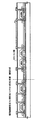
図1に示すとおり、チェック基板106が有する1次コイル形成部と、アレイ基板(TFT基板)100が有する2次コイル形成部104は、一定の間隔を空けて重ねられている。
【0051】
1次コイル形成部と2次コイル形成部104とが重なっている部分の拡大図を、図23(C)に示す。図23(C)において、1次コイル107と2次コイル104は、配線の渦の巻く方向が同じになっているが、本発明はこの構成に限定されない。1次コイルと2次コイルの渦の巻く方向が逆であっても良い。
【0052】
チェック基板とアレイ基板とが一定の間隔を保つため、本実施形態では、チェック基板に気体を一定の圧力で流入させることで、チェック基板とアレイ基板との間隔を保つ方法を用いる。この間隔は、実施者が適宜決定すればよいが、本実施形態では、10〜200μmの間隔とするのが好ましい。また、気体を流入するために、チェック基板には気体を流入させる穴110を複数形成する。
【0053】
アレイ基板とチェック基板との間隔を一定に保つために気体以外にも絶縁性の液体を用いることもできる。
【0054】
また、検査装置には、駆動電源および駆動信号を入力する装置111、光源(ハロゲンランプ、放電灯等の干渉性を有さない光源を用いればよい)112a、光学系112b、ビデオカメラ113、画像処理装置114が設けられており、TFTに電圧を印加する前に、この光源112からの光を照射してポッケルスセル表面からの光の様子を画像としてビデオカメラ113で捉えて画像処理すればよい。
【0055】
チェック基板106が有するアレイ基板(TFT基板)に形成された回路または回路素子の動作情報を検出する手段は、液晶もしくはポッケルスセル108のような電界の変化により光学特性の変化する材料である。チェック基板106において、ポッケルス結晶は第1電極109aと第2電極109bに挟まれている(図22)。
【0056】
ポッケルスセルとは、電気光学効果(ポッケルス効果)を有する光学素子であって、電圧をかけると、電気光学的特性が変化するという性質を利用した素子である。この性質を利用し、結晶に交流電圧やパルス電圧を加えて、光の変調やシャッター、円偏光の発生や検出に用いることができる。具体的には、NH4H2PO4、BaTiO3、KH2PO(KHP)、KD2PO4(D・KDP)、LiNbO3、ZnTeまたはZnOの結晶体である。
【0057】
アレイ基板上の回路または回路素子が駆動して電界が変化し、その電界の変化によりポッケルスセルにおいて複屈折が生じて透過率が異なってみえる。すなわち、正常な回路または回路素子と重なる部分のポッケルスセルに比べて、欠陥のある回路または回路素子と重なる部分のポッケルスセルは、明るく見えたり暗く見えたりする。
【0058】
例えば、画素に形成された欠陥が生じていない正常なTFTと欠陥が生じているTFTとでは、光の透過率が異なる。これは、ポッケルスセルが有する強誘電体結晶の光軸に対して垂直になるように素子基板を配置すると、回路または回路素子において生じる電界により、強誘電体結晶において複屈折が生じるためである。
【0059】
この複屈折の、電界方向成分をもつ偏光に対する屈折率は、電界の強さによって決まる。よって、同じ構造を有し、なおかつ正常に動作している複数の回路または回路素子においては、同じ強さの電界が生じているため、各回路または回路素子と重なる部分における強誘電体結晶の屈折率は、ほぼ等しくなる。
【0060】
しかし、欠陥のある回路または回路素子において生じる電界は、他の正常な回路または回路素子において生じる電界に比べて、強かったり弱かったりする。よって、欠陥のある回路または回路素子と重なる部分における強誘電体結晶の屈折率は、他の正常な回路または回路素子と重なる部分における強誘電体結晶の屈折率と異なる。よって、ポッケルスセルを通して素子基板を見たときに、欠陥のある回路または回路素子と重なる部分が、正常な回路または回路素子と重なる部分に比べて、明るく見えたり、暗く見えたりする。
【0061】
例えば、図1に示すように、アレイ基板に対して垂直な方向における光を、偏光ビームスプリッターなどの光学系を用いて分離し、その強度をモニターすることで、ポッケルスセルの透過率を算出し、欠陥箇所を検出することが可能である。なお、複数回にわたるモニターの結果に何らかの演算処理を施し、欠陥箇所を検出するようにしても良い。
【0062】
また、検査対象である全ての回路の出力を検査専用回路に入力し、該検査専用回路において生じる電界の強度を、電気光学素子を用いて測定することで、欠陥の有無を特定したり、欠陥箇所そのものを特定したりしても良い。検査専用回路を用いることで、検査対象である全ての回路または回路素子において、いちいちポッケルス・セルを用いてモニターする必要がなくなり、検査工程を簡便化及び迅速化することができる。
【0063】
なお、欠陥の検出は画素部に限定されず、どの回路や回路素子においても本検査方法を適用することができる。例えば、ポッケルスセルと、駆動回路や信号線駆動回路を重ね合わせ、屈折率をモニターすることで、同じように欠陥箇所を検出することが可能である。また素子基板上の引きまわし配線において生じる断線やショートなどの欠陥も、同様に検出することが可能である。
【0064】
以上のような検査工程により、アレイ基板上の各TFT基板に対して、製品化の可否を確認する。この後、検査工程前に帯電防止膜を塗布した場合はこの帯電防止膜を除去し、有機絶縁膜をエッチングしてバンク207を形成し、230〜350℃で加熱処理を行う。
【0065】
次いで、アレイ基板100を分断してTFT基板101とする。アレイ基板上にTFT基板および検査用回路(2次コイル、整流回路および波形整形回路)をどのように形成するかは、実施者が適宜決定すればよいが、図5に示すようにTFT基板と検査工程で用いた2次コイル、整流回路および波形整形回路が駆動回路と電気的かつ物理的な接続を残さないように分断できるようにしておくことが好ましい。
【0066】
続いて、上記検査工程において、製品化可能と判断されたTFT基板101の画素電極206上に絶縁膜208、有機化合物層209、陰極210を形成する。製品化できないと判断されたTFT基板は、製造工程からはずし不良解析を行ったり、修復して製品化が可能であれば修復し、再度検査工程に戻してもよい。
【0067】
絶縁膜208は、ポリイミド、ポリアミド、アクリル等の有機樹脂絶縁膜をスピンコート法を用いて、1〜5nmの膜厚で形成する。
有機化合物層209は、発光層の他に正孔注入層として、正孔輸送層、正孔阻止層、電子輸送層、電子注入層およびバッファー層といった複数の層を組み合わせて積層し形成される。有機化合物層209としての膜厚は、10〜400nm程度が好ましい。
陰極210は、有機化合物層209成膜後に、蒸着法により形成する。陰極210となる材料としては、MgAgやAl−Li合金(アルミニウムとリチウムの合金)の他に、周期表の1族もしくは2族に属する元素とアルミニウムとを共蒸着法により形成した膜を用いても良い。なお、陰極210の膜厚は、80〜200nm程度が好ましい。
【0068】
以上のようにして、アレイ基板100上に複数形成されたTFT基板101を用いて発光装置を作製することができる。
【0069】
なお、本実施形態において、アレイ基板はガラス基板を用いているが、石英基板またはプラスチック基板を用いてもよい。ただし、プラスチック基板を用いる場合は、基板の耐熱温度が低いため、プラスチック基板が耐えうる温度で行える作製プロセスを実施者が適宜決定すればよい。
【0070】
なお、チェック基板およびアレイ基板に形成されるコイルの巻き数、線幅、形状および基板上にしめる面積は、実施者が適宜決定することができるが、1次コイルの巻き数に対する2次コイルの巻き数の割合は、1次コイルに印加される電圧が2次コイルに誘導される電圧の割合に反比例することを考慮して設計することが重要である。
【0071】
(実施形態2)
本実施形態では、TFT基板の他の検査方法について、図4、6を用いて説明する。
【0072】
本実施形態において開示する検査方法は、アレイ基板上に形成されたTFT基板の回路および回路素子が動作する際に、電磁波が発生する。この電磁波の強度、周波数、ある時間毎の電磁波の強度、周波数を測定することでTFT基板の製品化の可否を確認する方法である。
【0073】
あらかじめ、良品(製品化可能)と判断されたTFT基板の回路の電磁波の強度、周波数および時間毎の強度、周波数を測定して、TFT基板の製品化可否の判断の際の比較に用いればよい。
【0074】
次いで、アレイ基板に形成されたTFT基板の回路および回路素子に電磁誘導を利用して、電源電圧および駆動信号を供給する。この時の電磁波の強度、周波数および時間毎(あるタイミング毎)の強度と周波数を電磁波の測定可能なアンテナを有するチェック基板を用いて測定する。
【0075】
なお、チェック基板には、実施形態1と同様に1次コイルが形成されており、駆動電源および駆動信号入力装置から1次コイルが有する2つの端子間に交流電圧を印加すると2次コイルが有する2つの端子間に起電力が生じる。
【0076】
次いで、2次コイルに生じた起電力である交流電圧をアレイ基板に形成された整流回路により整流化し平滑化することでアレイ基板が有する回路または回路素子を駆動させるための直流電圧(以下、電源電圧と称する)として用いることができる。さらに、2次コイルに生じた起電力である交流電圧をアレイ基板に形成された波形整形回路により適当に電圧を信号波形に整形することで、アレイ基板上の回路または回路素子を駆動させるための信号(以下、駆動信号と称する)として用いることができる。
【0077】
実施形態1で説明したように整流回路および波形整形回路により駆動電源および駆動信号が供給されると、TFT基板に形成された回路および回路素子が動作し、電磁波が発生する。この発生した電磁波の強度、スペクトルおよびタイミング毎の電磁波の強度、スペクトルをチェック基板に設けられたアンテナ303で測定する。チェック基板301に設けられた電磁波センサー(アンテナともいう)303は、計測周波数帯域が1MHz〜1GHzの公知のセンサー(アンテナ)を用いればよい。また、チェック基板がアレイ基板に接触しないようにするため、さらにアレイ基板上の回路または回路素子が発する電磁波の測定再現性を向上させるために、チェック基板が常にアレイ基板と一定の間隔を保つ必要がある。本実施形態では、チェック基板に気体を一定の圧力で吹き込みチェック基板とアレイ基板との間隔を一定に保っている。この間隔は、実施者が適宜決定すればよいが、本実施形態では、10〜200μmの間隔としている。気体を吹き込むために、チェック基板には気体を吹き込む穴110が複数形成されている。アレイ基板100およびチェック基板301におけるコイルと端子の関係概略図は図4のとおりである。
【0078】
アンテナ303は、アレイ基板に形成された微細な回路および回路素子から発生する電磁波の強度、周波数等の位置情報を得るのに必要な分解能にするため、チェック基板にアンテナを形成する間隔をなるべく狭くして、より多くの小型アンテナを形成することが好ましい。アンテナを形成する間隔は、画素サイズに合わせて最適な分解能が得られるように実施者が適宜決定すればよい。
また、チェック基板とアレイ基板との間隔もなるべく狭く、本実施形態では100μm以下で、一定に保つことで分解能を向上させることができる。
【0079】
本実施形態で開示する検査方法は、アレイ基板上に形成された回路および回路素子の動作を回路および回路素子が発する電磁波の強度、周波数、および時間毎の電磁波の強度、周波数を一度に測定して確認するため、短時間でTFT基板の良品確認をすることができる。
【0080】
本実施形態で示した検査工程が終了したら、アレイ基板100をひとつひとつのTFT基板101に分断した後、製品化可能と判断されたTFT基板上に発光素子を形成してELディスプレイを作製したり、TFT基板と対向基板とを張り合わせて液晶を封入して液晶ディスプレイを作製したりすればよい。
【0081】
このような検査工程を作製工程に組み込むことにより、不良画素または不良駆動回路を多数含んだTFT基板に関しては、発光素子の形成工程を行わないため、無駄に発光素子形成材料を用いることが無いため、製造コストを低減することができる。
【0082】
また、非接触でアレイ基板に駆動電源または駆動信号を送ることができるため、検査工程(または検査工程準備)の際にアレイ基板にゴミが付着して汚染されるという問題も解決することができる。
【0083】
【実施例】
(実施例1)
本実施例においては、本発明を用いて作製される発光素子について説明する。なお、ここでは、同一基板上に本発明の発光素子を有する画素部と、画素部の周辺に設ける駆動回路のTFT(nチャネル型TFT及びpチャネル型TFT)と、TFT基板の駆動を検査するためのトランスの2次コイル、整流回路および波形整形回路を同一基板上に作製する方法の一例について図7〜10を用いて説明する。
【0084】
まず、本実施例ではコーニング社の#7059ガラスや#1737ガラスなどに代表されるバリウムホウケイ酸ガラス、またはアルミノホウケイ酸ガラスなどのガラスからなる基板900を用いる。なお、基板900としては、透光性を有する基板であれば限定されず、石英基板を用いても良い。また、本実施例の処理温度に耐えうる耐熱性を有するプラスチック基板を用いてもよい。
【0085】
次いで、図7(A)に示すように、基板900上に酸化珪素膜、窒化珪素膜または酸化窒化珪素膜などの絶縁膜から成る下地絶縁膜901を形成する。本実施例では下地絶縁膜901として2層構造を用いるが、前記絶縁膜の単層膜または2層以上積層させた構造を用いても良い。下地絶縁膜901の一層目としては、プラズマCVD法を用い、SiH4、NH3、及びN2Oを反応ガスとして成膜される酸化窒化珪素膜901aを10〜200nm(好ましくは50〜100nm)形成する。本実施例では、膜厚50nmの酸化窒化珪素膜901a(組成比Si=32%、O=27%、N=24%、H=17%)を形成した。次いで、下地絶縁膜901のニ層目としては、プラズマCVD法を用い、SiH4、及びN2Oを反応ガスとして成膜される酸化窒化珪素膜901bを50〜200nm(好ましくは100〜150nm)の厚さに積層形成する。本実施例では、膜厚100nmの酸化窒化珪素膜901b(組成比Si=32%、O=59%、N=7%、H=2%)を形成した。
【0086】
次いで、下地絶縁膜901上に半導体層902〜906を形成する。半導体層906は、整流回路においてTFTを変形させてダイオードを形成するための半導体層である。なお、本明細書中において、チャネル形成領域、後のソース領域、ドレイン領域となるn型不純物を高濃度に添加された領域を含む半導体層を活性層ともいう。半導体層902〜906は、非晶質構造を有する半導体膜を公知の手段(スパッタ法、LPCVD法、またはプラズマCVD法等)により成膜した後、公知の結晶化処理(レーザー結晶化法、熱結晶化法、またはニッケルなどの触媒を用いた熱結晶化法等)を行って得られた結晶質半導体膜を所望の形状にパターニングして形成する。この半導体層902〜906の厚さは25〜80nm(好ましくは30〜60nm)の厚さで形成する。結晶質半導体膜の材料に限定はないが、好ましくは珪素(シリコン)またはシリコンゲルマニウム(SiXGe1-X(X=0.0001〜0.02))合金などで形成すると良い。本実施例では、プラズマCVD法を用い、55nmの非晶質珪素膜を成膜した後、ニッケルを含む溶液を非晶質珪素膜上に保持させた。この非晶質珪素膜に脱水素化(500℃、1時間)を行った後、熱結晶化(550℃、4時間)を行い、さらに結晶化を改善するためのレーザーアニ―ル処理を行って結晶質珪素膜を形成した。そして、この結晶質珪素膜をフォトリソグラフィー法を用いたパターニング処理によって、半導体層902〜906を形成した。
【0087】
また、半導体層902〜906を形成した後、TFTのしきい値を制御するために、半導体層902〜906に微量な不純物元素(ボロンまたはリン)をドーピングしてもよい。
【0088】
また、レーザー結晶化法で結晶質半導体膜を作製する場合には、パルス発振型または連続発光型のエキシマレーザーやYAGレーザー、YVO4レーザーを用いることができる。これらのレーザーを用いる場合には、レーザー発振器から放射されたレーザー光を光学系で線状に集光し半導体膜に照射する方法を用いると良い。結晶化の条件は実施者が適宣選択するものであるが、エキシマレーザーを用いる場合はパルス発振周波数300Hzとし、レーザーエネルギー密度を100〜400mJ/cm2(代表的には200〜300mJ/cm2)とする。また、YAGレーザーを用いる場合にはその第2高調波を用いパルス発振周波数30〜300kHzとし、レーザーエネルギー密度を300〜600mJ/cm2(代表的には350〜500mJ/cm2)とすると良い。そして幅100〜1000μm、例えば400μmで線状に集光したレーザー光を基板全面に渡って照射し、この時の線状レーザー光の重ね合わせ率(オーバーラップ率)を50〜90%として行えばよい。
【0089】
次いで、半導体層902〜906を覆うゲート絶縁膜907を形成する。ゲート絶縁膜907はプラズマCVD法またはスパッタ法を用い、厚さを40〜150nmとして珪素を含む絶縁膜で形成する。本実施例では、プラズマCVD法により110nmの厚さで酸化窒化珪素膜(組成比Si=32%、O=59%、N=7%、H=2%)で形成した。勿論、ゲート絶縁膜は酸化窒化珪素膜に限定されるものでなく、他の珪素を含む絶縁膜を単層または積層構造として用いても良い。
【0090】
また、酸化珪素膜を用いる場合には、プラズマCVD法でTEOS(Tetraethyl Orthosilicate)とO2とを混合し、反応圧力40Pa、基板温度300〜400℃とし、高周波(13.56MHz)電力密度0.5〜0.8W/cm2で放電させて形成することができる。このようにして作製される酸化珪素膜は、その後400〜500℃の熱アニールによりゲート絶縁膜として良好な特性を得ることができる。
【0091】
そして、ゲート絶縁膜907上にゲート電極を形成するための耐熱性導電層908を200〜400nm(好ましくは250〜350nm)の厚さで形成する。耐熱性導電層908は単層で形成しても良いし、必要に応じて二層あるいは三層といった複数の層から成る積層構造としても良い。耐熱性導電層にはTa、Ti、Wから選ばれた元素、または前記元素を成分とする合金か、前記元素を組み合わせた合金膜が含まれる。これらの耐熱性導電層はスパッタ法やCVD法で形成されるものであり、低抵抗化を図るために含有する不純物濃度を低減させることが好ましく、特に酸素濃度に関しては30ppm以下とすると良い。本実施例ではW膜を300nmの厚さで形成する。W膜はWをターゲットとしてスパッタ法で形成しても良いし、6フッ化タングステン(WF6)を用いて熱CVD法で形成することもできる。いずれにしてもゲート電極として使用するためには低抵抗化を図る必要があり、W膜の抵抗率は20μΩcm以下にすることが望ましい。W膜は結晶粒を大きくすることで低抵抗率化を図ることができるが、W中に酸素などの不純物元素が多い場合には結晶化が阻害され高抵抗化する。このことより、スパッタ法による場合、純度99.9〜99.9999%のWターゲットを用い、さらに成膜時に気相中からの不純物の混入がないように十分配慮してW膜を形成することにより、抵抗率9〜20μΩcmを実現することができる。
【0092】
一方、耐熱性導電層908にTa膜を用いる場合には、同様にスパッタ法で形成することが可能である。Ta膜はスパッタガスにArを用いる。また、スパッタ時のガス中に適量のXeやKrを加えておくと、形成する膜の内部応力を緩和して膜の剥離を防止することができる。α相のTa膜の抵抗率は20μΩcm程度でありゲート電極に使用することができるが、β相のTa膜の抵抗率は180μΩcm程度でありゲート電極とするには不向きであった。TaN膜はα相に近い結晶構造を持つので、Ta膜の下地にTaN膜を形成すればα相のTa膜が容易に得られる。また、図示しないが、耐熱性導電層908の下に2〜20nm程度の厚さでリン(P)をドープしたシリコン膜を形成しておくことは有効である。これにより、その上に形成される導電膜の密着性向上と酸化防止を図ると同時に、耐熱性導電層908、909中に微量に存在しているアルカリ金属元素が第1の形状のゲート絶縁膜907に拡散するのを防ぐことができる。いずれにしても、耐熱性導電層908は抵抗率を10〜50μΩcmの範囲ですることが好ましい。
【0093】
さらに、ゲート電極を形成する他の例として、第1の導電膜としてリン等の不純物元素をドーピングした多結晶シリコン膜に代表される半導体膜を用いてもよい。また、第1の導電膜をタングステン(W)膜で形成し、第2の導電膜をCu膜、第3の導電膜をチタン(Ti)膜とする組み合わせ、第1の導電膜をタンタル(TaN)膜で形成し、第2の導電膜をアルミニウム(Al)膜、第3の導電膜をチタン(Ti)膜とする組み合わせ、第1の導電膜を窒化タンタル(TaN)膜で形成し、第2の導電膜をAl膜とする組み合わせ、第1の導電膜を窒化タンタル(TaN)膜で形成し、第2の導電膜をCu膜、第3の導電膜をチタン(Ti)とする組み合わせとする3層構造のゲート電極を採用してもよい。
【0094】
本実施例においては、第1層目の導電層(第1導電膜908)にTaN膜、第2層目の導電層(第2導電膜909)にW膜を形成した(図7(A))。
【0095】
次に、フォトリソグラフィーの技術を使用してゲート電極を形成するためのレジストによるマスク910aおよび2次コイルを形成するためのレジストによるマスク910bを形成する。そして、第1のエッチング処理を行う。第1のエッチング処理は、第1のエッチング条件および第2のエッチング条件で行われる。
【0096】
本実施例ではICPエッチング装置を用い、エッチング用ガスにCl2とCF4O2を用い、それぞれのガス流量比を25/25/10とし、1Paの圧力で3.2W/cm2のRF(13.56MHz)電力を投入してプラズマを形成して行う。基板側(試料ステージ)にも224mW/cm2のRF(13.56MHz)電力を投入し、これにより実質的に負の自己バイアス電圧が印加される。第1のエッチング条件によりW膜をエッチングする。続いて、レジストからなるマスクを除去せずに第2のエッチング条件に変えてエッチング用ガスにCF4およびCl2を用いて、それぞれのガス流量比を30/30(SCCM)とし、1Paの圧力でRF(13.56MHz)電力を投入してプラズマを形成して行う。基板側(試料ステージ)にも20WのRF(13.56MHz)電力を投入し、実質的に負の自己バイアス電圧を印加する。
【0097】
第1のエッチング処理により第1のテーパ形状を有する導電層911〜915が形成される。導電層911〜915のテーパの角度は15〜30°となるように形成される。残渣を残すことなくエッチングするためには、10〜20%程度の割合でエッチング時間を増加させるオーバーエッチングを施すものとする。W膜に対する酸化窒化シリコン膜(ゲート絶縁膜907)の選択比は2〜4(代表的には3)であるので、オーバーエッチング処理により、酸化窒化シリコン膜が露出した面は20〜50nm程度エッチングされる。
【0098】
そして、第1のドーピング処理を行い一導電型の不純物元素を半導体層に添加する。ここでは、レジストからなるマスク910を除去せずにn型を付与する不純物元素添加の工程を行う。半導体層902〜906の一部に第1のテーパ形状を有する導電膜911〜915をマスクとして自己整合的に不純物を添加し、第1のn型不純物領域916〜920を形成する。n型を付与する不純物元素として15族に属する元素、典型的にはリン(P)または砒素(As)を用いるが、ここではリン(P)を用い、イオンドープ法により第1のn型不純物領域916〜920には1×10²⁰〜1×10²¹atoms/cm3の濃度範囲でn型を付与する不純物元素が添加される(図7(B))。
【0099】
次にレジストからなるマスクを除去せずに第2のエッチング処理を行う。第2のエッチング処理は、第3のエッチング条件および第4のエッチング条件で行う。第2のエッチング処理も第1のエッチング処理と同様にICPエッチング装置により行い、エッチングガスにCF4およびCl2を用い、それぞれのガス流量比を30/30(SCCM)とし、1Paの圧力でRF(13.56MHz)電力を投入してプラズマを形成して行う。基板側(試料ステージ)にも20WのRF(13.56MHz)電力を投入し、実質的に負の自己バイアス電圧を印加する。この第3のエッチング条件により、W膜およびTaN膜とも同程度にエッチングされた導電膜921〜925が形成される(図7(C))。
【0100】
この後、レジストからなるマスクをそのままに第4のエッチング条件に変えて、エッチング用ガスにCF4とCl2およびO2の混合ガスを用い、1Paの圧力でRF電力(13.56MHz)電力を投入してプラズマを形成して行う。基板側(試料ステージ)にも20WのRF(13.56MHz)電力を投入し、実質的に負の自己バイアス電圧を印加する。この第4のエッチング条件でW膜をエッチングして、第2の形状の導電膜926〜930を形成する(図7(D))。
【0101】
なお、本実施例において2次コイルはゲート電極を形成するためのエッチング処理がすべて終了した後に、渦巻き状のマスクを用いてエッチングして形成すればよい。従って、ゲート電極を形成する領域は、エッチング処理中はマスクで覆っておく。また、渦巻き状のマスクは、2次コイルが外径1mm、内径0.5mmになるように形成しているが、2次コイルの形状は円形の渦巻きに限定されるものではなく、実施者が適宜決定すればよい。また、各TFT基板に形成する2次コイルの数は、TFT基板の駆動電圧にあわせて実施者が適宜決定すればよい。さらに、2次コイルを形成する方法も、本実施例に限定されるものではなく、実施者が決定すればよい。
【0102】
次いで、第2のドーピング工程(第2の形状の第1の導電膜926a〜930aを介して半導体層にn型不純物元素の添加)を行い、第1のn型不純物領域916〜920と接するチャネル形成領域側に第2のn型不純物領域933〜937とを形成する。第2のn型不純物領域における不純物濃度は、1×10¹⁶〜1×10¹⁹atoms/cm3となるようにする。この第2のドーピング工程においては、1層目の第2の形状の導電膜926a〜930aのテーパ部を介しても半導体層にn型不純物元素が添加されるような条件になっており、本明細書において、1層目の第2の形状の導電膜926a〜930aと重なる第2のn型不純物領域をLov(ovはoverlappedの意味で付す)領域、1層目の第2の形状の導電膜926a〜930aとは重ならない第2のn型不純物領域をLoff(offはoffsetの意味で付す)ということとする(図8(A))。
【0103】
次いで、図8(B)に示すように、後のpチャネル型TFTの活性層(チャネル形成領域およびソース・ドレイン領域となる高濃度に不純物が添加された領域を含めた半導体層)となる半導体層902、905、906に一導電型とは逆の導電型の不純物領域939(939a、939b)、940(940a、940b)及び933(9323a、933b)を形成する。第2の形状の導電層926、929、930をマスクとしてp型を付与する不純物元素を添加し、自己整合的に不純物領域を形成する。このとき、後のnチャネル型TFTの活性層となる半導体層903、904は、レジストからなるマスク938a、938bを形成し全面を被覆しておく。ここで形成されるp型不純物領域939、940、941はジボラン(B2H6)を用いたイオンドープ法で形成し、p型不純物領域939、940、941のp型を付与する不純物元素の濃度は、2×10²⁰〜2×10²¹atoms/cm3となるようにする。
【0104】
p型不純物領域939、940、941には詳細にはn型を付与する不純物元素が含有されているが、これらの不純物領域939、940、941のp型を付与する不純物元素の濃度は、n型を付与する不純物元素の濃度の1.5から3倍となるように添加されることによりp型不純物領域でpチャネル型TFTのソース領域およびドレイン領域として機能するために何ら問題は生じない。
【0105】
その後、図8(C)に示すように、第2の形状を有する導電層926〜930およびゲート絶縁膜上に第1の層間絶縁膜942を形成する。第1の層間絶縁膜942は窒化シリコン膜、酸化シリコン膜、酸化窒化シリコン膜、またはこれらを組み合わせた積層膜で形成すれば良い。いずれにしても第1の層間絶縁膜942は無機絶縁材料から形成する。第1の層間絶縁膜942の膜厚は100〜200nmとする。第1の層間絶縁膜942として酸化シリコン膜を用いる場合には、プラズマCVD法でTEOSとO2とを混合し、反応圧力40Pa、基板温度300〜400℃とし、高周波(13.56MHz)電力密度0.5〜0.8W/cm2で放電させて形成することができる。また、第1の層間絶縁膜942として酸化窒化シリコン膜を用いる場合には、プラズマCVD法でSiH4、N2O、NH3から作製される酸化窒化シリコン膜、またはSiH4、N2Oから作製される酸化窒化シリコン膜で形成すれば良い。この場合の作製条件は反応圧力20〜200Pa、基板温度300〜400℃とし、高周波(60MHz)電力密度0.1〜1.0W/cm2で形成することができる。また、第1の層間絶縁膜942としてSiH4、N2O、H2から作製される酸化窒化水素化シリコン膜を適用しても良い。窒化シリコン膜も同様にプラズマCVD法でSiH4、NH3から作製することが可能である。
【0106】
そして、それぞれの濃度で添加されたn型またはp型を付与する不純物元素を活性化する工程を行う。この工程はファーネスアニール炉を用いる熱アニール法で行う。その他に、レーザーアニール法、またはラピッドサーマルアニール法(RTA法)を適用することができる。熱アニール法では酸素濃度が1ppm以下、好ましくは0.1ppm以下の窒素雰囲気中で400〜700℃、代表的には500〜600℃で行うものであり、本実施例では550℃で4時間の加熱処理を行った。また、基板900に耐熱温度が低いプラスチック基板を用いる場合にはレーザーアニール法を適用することが好ましい。
【0107】
この加熱処理工程において、半導体層を結晶化させる工程で用いた触媒元素(ニッケル)が、ゲッタリング作用を有する周期表の15族に属する元素(本実施例ではリン)が高濃度に添加された第1のn型不純物領域に移動(ゲッタリング)させ、チャネル形成領域における触媒元素の濃度を低減することができる。
【0108】
活性化の工程に続いて、雰囲気ガスを変化させ、3〜100%の水素を含む雰囲気中で、300〜450℃で1〜12時間の加熱処理を行い、半導体層を水素化する工程を行う。この工程は熱的に励起された水素により半導体層にある1016〜1018/cm3のダングリングボンドを終端する工程である。水素化の他の手段として、プラズマ水素化(プラズマにより励起された水素を用いる)を行っても良い。いずれにしても、半導体層902〜906中の欠陥密度を1016/cm3以下とすることが望ましく、そのために水素を0.01〜0.1atomic%程度付与すれば良い。
【0109】
そして、有機絶縁物材料からなる第2の層間絶縁膜943を1.0〜2.0μmの平均膜厚で形成する。有機樹脂材料としては、ポリイミド、アクリル、ポリアミド、ポリイミドアミド、BCB(ベンゾシクロブテン)等を使用することができる。例えば、基板に塗布後、熱重合するタイプのポリイミドを用いる場合には、クリーンオーブンで300℃で焼成して形成する。また、アクリルを用いる場合には、2液性のものを用い、主材と硬化剤を混合した後、スピナーを用いて基板全面に塗布した後、ホットプレートで80℃で60秒の予備加熱を行い、さらにクリーンオーブンで250℃で60分焼成して形成することができる。
【0110】
このように、第2の層間絶縁膜943を有機絶縁物材料で形成することにより、表面を良好に平坦化させることができる。また、有機樹脂材料は一般に誘電率が低いので、寄生容量を低減できる。しかし、吸湿性があり保護膜としては適さないので、本実施例のように、第1の層間絶縁膜942として形成した酸化シリコン膜、酸化窒化シリコン膜、窒化シリコン膜などと組み合わせて用いると良い。
さらに、本実施例では、第2層間絶縁膜943を有機絶縁物材料で形成したが、無機絶縁材料を用いて形成し、その表面をCMP法等で平坦化して得られる膜を第2層間絶縁膜としてもよい。
【0111】
ところで、有機絶縁材料を用いて形成される第2の層間絶縁膜943は、水分やガスを発生してしまう可能性がある。発光素子は水分やガス(酸素)で劣化しやすいことが知られている。実際に層間絶縁膜に有機樹脂絶縁膜を用いて形成された発光装置が使用する際に発生する熱で、有機樹脂絶縁膜から水分やガスが発生し、発光素子の劣化が起こりやすくなってしまうことが考えられる。そこで、有機絶縁材料で形成された第2の層間絶縁膜943上に絶縁膜944を形成する。
なお、絶縁膜944は、酸化シリコン膜、酸化窒化シリコン膜、窒化シリコン膜などを用いて形成される。なおここで形成される絶縁膜944はスパッタ法またはプラズマCVD法を用いて形成すればよい。また、絶縁膜944は、コンタクトホールを形成した後から形成してもよい。
【0112】
その後、所定のパターンのレジストマスクを形成し、それぞれの半導体層に形成されソース領域またはドレイン領域とする不純物領域に達するコンタクトホールを形成する。コンタクトホールはドライエッチング法で形成する。
【0113】
そして、導電性の金属膜をスパッタ法や真空蒸着法で形成し、マスクでパターニングし、その後エッチングすることで、配線945〜952を形成する。図示していないが、本実施例ではこの配線を、そして、膜厚50nmのTi膜と、膜厚500nmの合金膜(AlとTiとの合金膜)との積層膜で形成した。
【0114】
次いで、その上に透明性導電膜を80〜120nmの厚さで形成し、エッチングすることによって画素電極(陽極)953を形成する(図9(A))。なお、本実施例では、透明電極として酸化インジウム・スズ(ITO)膜や酸化インジウムに2〜20[%]の酸化亜鉛(ZnO)を混合した透明導電膜を用いる。
【0115】
また、陽極953は、ドレイン配線950と接して重ねて形成することによって電流制御用TFTのドレイン領域と電気的な接続が形成される。ここで、陽極953に対して180〜350℃で加熱処理を行ってもよい。
【0116】
次に、図9(B)に示すように、陽極953上に有機絶縁膜954を形成する。
【0117】
ここまでの工程でTFTが形成されたアレイ基板が空気中のゴミに汚染されたり、破壊したりしないように有機絶縁膜954上に、帯電防止作用を有する極薄い膜(以下、帯電防止膜という)955を形成する。帯電防止膜955は、水洗で除去可能な公知の材料から形成する(図9(C))。
本実施例では、スタティサイド(ACL社製)を塗布して帯電防止膜955を形成した。
【0118】
次いで、ここまでの工程で作製されたアレイ基板上のTFTの良否(TFT基板の製品化の可否)を判断するための検査を行う。発光素子を形成する材料は高価であるので、商品として出荷できないTFT基板に発光素子を形成してしまうのは、製造コストの面で問題がある。そこで、正常に駆動できないもしくは信号伝達のできないTFT基板を見分けるために検査工程を組み込む。検査方法は、実施形態1もしくは実施形態2に示したような検査方法を適応すればよい。
【0119】
TFT基板を発光素子を形成する処理室(クリーンルーム)に運びこんだら、帯電防止膜955を水洗して除去する。次いで、有機絶縁膜954をエッチングして、画素(発光素子)に対応する位置に開口部を有するバンク956を形成する。本実施例ではレジストを用いてバンク956を形成する。本実施例では、バンク956の厚さを1μm程度とし、配線と陽極とが接する部分を覆う領域がテーパ状になるように形成する(図10(A))。
【0120】
なお、本実施例においては、バンク956としてレジストでなる膜を用いているが、場合によっては、ポリイミド、ポリアミド、アクリル、BCB(ベンゾシクロブテン)、酸化珪素膜等を用いることもできる。バンク956は絶縁性を有する物質であれば、有機物と無機物のどちらでも良いが、感光性アクリルを用いてバンク956を形成する場合は、感光性アクリル膜をエッチングしてから180〜350℃で加熱処理を行うのが好ましい。また、非感光性アクリル膜を用いて形成する場合には、180〜350℃で加熱処理を行った後、エッチングしてバンクを形成するのが好ましい。
【0121】
次に、陽極表面に拭浄処理を行う。なお、本実施例においては、ベルクリン(小津産業製)を用いて陽極953表面を拭うことにより、陽極953表面の平坦化および表面に付着したゴミの除去を行う。拭浄の際の洗浄液としては、純水を用い、ベルクリンを巻き付けている軸の回転数は100〜300rpmとし、押し込み値は0.1〜1.0mmとする(図10(A))。
【0122】
次いで、バンク956および陽極953を覆って絶縁膜957を形成する。絶縁膜957は、ポリイミド、ポリアミド、ポリイミドアミドなどの有機樹脂膜をスピンコート法、蒸着法またはスパッタ法などを用いて膜厚1〜5nmで形成する。この絶縁膜を形成することで、陽極953表面のクラック等を掩蔽することができ、発光素子の劣化を防ぐことができる。
【0123】
この後、公知の方法でアレイ基板を複数のTFT基板に分断する。この時、製品化するTFT基板領域より外側に形成してある検査工程で用いたトランス2次コイル、整流回路および波形整形回路を電気的かつ物理的に分断しておくことが好ましい。なお、本実施例ではトランス2次コイル、整流回路および波形整形回路を製品化するTFT基板領域より外側に形成したが、これらを形成する場所は実施者が適宜決定すればよく、本実施例に限定されない。
【0124】
次いで、製品化が可能なTFT基板の絶縁膜957上に有機化合物層958、陰極959を蒸着法により形成する。なお、本実施例では発光素子の陰極としてMgAg電極を用いるが、公知の他の材料であっても良い。なお、有機化合物層949は、発光層の他に正孔注入層、正孔輸送層、電子輸送層、電子注入層及びバッファー層といった複数の層を組み合わせて積層することにより形成されている。本実施例において用いた有機化合物層の構造について以下に詳細に説明する。
【0125】
本実施例では、正孔注入層として、銅フタロシアニンを用い、正孔輸送層としては、α−NPDを用いてそれぞれ蒸着法により形成する。
【0126】
次に、発光層が形成されるが、本実施例では発光層に異なる材料を用いることで異なる発光を示す有機化合物層の形成を行う。なお、本実施例では、赤、緑、青色の発光を示す有機化合物層を形成する。また、成膜法としては、いずれも蒸着法を用いているので、成膜時にメタルマスクを用いることにより画素毎に異なる材料を用いて発光層を形成することは可能である。
【0127】
赤色に発色する発光層は、Alq3にDCMをドーピングしたものを用いて形成する。その他にもN,N'-ジサリチリデン−1,6−ヘキサンジアミナト)ジンク(II)(Zn(salhn))にEu錯体である(1,10-フェナントロリン)トリス(1,3-ジフェニル−プロパン−1,3-ジオナト)ユーロピウム(III)(Eu(DBM)3(Phen)をドーピングしたもの等を用いることができるが、その他公知の材料を用いることもできる。
【0128】
また、緑色に発色する発光層は、CBPとIr(ppy)3を共蒸着法により形成させることができる。なお、この時には、BCPを用いて正孔阻止層を積層しておくことが好ましい。また、この他にもアルミキノリラト錯体(Alq3)、ベンゾキノリノラトベリリウム錯体(BeBq)を用いることができる。さらには、キノリラトアルミニウム錯体(Alq3)にクマリン6やキナクリドンといった材料をドーパントとして用いたものも可能であるが、その他公知の材料を用いることもできる。
【0129】
さらに、青色に発色する発光層は、ジスチリル誘導体であるDPVBiや、アゾメチン化合物を配位子に持つ亜鉛錯体であるN,N'−ジサリチリデン−1,6−ヘキサンジアミナト)ジンク(II)(Zn(salhn))及び4,4'−ビス(2,2−ジフェニル−ビニル)−ビフェニル(DPVBi)にペリレンをドーピングしたものを用いることもできるが、その他の公知の材料を用いても良い。
【0130】
次に電子輸送層を形成する。なお、電子輸送層としては、1,3,4−オキサジアゾール誘導体や1,2,4−トリアゾール誘導体(TAZ)といった材料を用いることができるが、本実施例では、1,2,4−トリアゾール誘導体(TAZ)を用いて蒸着法により30〜60nmの膜厚で形成する。
【0131】
以上により、積層構造からなる有機化合物層が形成される。なお、本実施例における有機化合物層958の膜厚は10〜400nm(典型的には60〜150nm)、陰極959の厚さは80〜200nm(典型的には100〜150nm)とすれば良い。
【0132】
有機化合物層を形成した後で、蒸着法により発光素子の陰極959が形成される。本実施例では発光素子の陰極となる導電膜としてMgAgを用いているが、Al−Li合金膜(アルミニウムとリチウムとの合金膜)や、周期表の1族もしくは2族に属する元素とアルミニウムとを共蒸着法により形成された膜を用いることも可能である。
【0133】
こうして図6(B)に示すような構造の発光装置が完成する。なお、陽極953、有機化合物層958、陰極959と積層された部分960を発光素子と称する(図10(B))。
【0134】
pチャネル型TFT1000及びnチャネル型TFT1001は駆動回路102のTFTであり、CMOSを形成している。スイッチング用TFT1002及び電流制御用TFT1003は画素部103のTFTであり、駆動回路102のTFTと画素部103のTFTとは同一基板上に形成することができる。
【0135】
なお、発光素子を用いた発光装置の場合、駆動回路の電源の電圧が5〜6V程度、最大でも10V程度で十分なので、TFTにおいてホットエレクトロンによる劣化は、あまり問題にならない。
【0136】
なお、本実施例では発光装置のTFT基板(TFT素子基板)に検査工程で用いるトランスの2次コイルを形成する一例を示しているが、発光装置に限らず、液晶表示装置等、半導体素子からなる半導体装置の素子基板上に本発明を適用するためのトランスの2次コイルを作り込むことが可能である。
【0137】
(実施例3)
実施例1に従い、第2の層間絶縁膜943まで形成する。次いで、実施例1における絶縁膜944を形成するかわりに、第2の層間絶縁膜にプラズマ処理を行って第2の層間絶縁膜935表面を改質させる方法について図11〜13で説明する。
【0138】
例えば、第2の層間絶縁膜943を水素、窒素、炭化水素、ハロゲン化炭素、弗化水素または希ガス(Ar、He、Ne等)から選ばれた一種または複数種の気体中でプラズマ処理することにより第2の層間絶縁膜943の表面に新たな被膜を形成したり、表面に存在する官能基の種類を変更させたりして、第2の層間絶縁膜943の表面改質を行うことができる。第2の層間絶縁膜943表面には、図11に示すように緻密化された膜943Bが形成される。本明細書において、この膜を硬化膜943Bと称する。これにより、有機樹脂膜からガスや水分が放出されるのを防ぐことができる。
【0139】
さらに、本実施例のように表面改質を行った後、陽極(ITO)を形成するため、熱膨張率の異なる材料が直接接した状態で加熱処理されることがなくなる。したがって、ITOのクラック(亀裂)等の発生を防ぐことができ、発光素子の劣化を防止することもできる。なお、第2の層間絶縁膜943のプラズマ処理化は、コンタクトホールを形成する前、後どちらでもよい。
【0140】
なお、硬化膜943Bは、有機絶縁材料からなる第2の層間絶縁膜943の表面を水素、窒素、炭化水素、ハロゲン化炭素、弗化水素または希ガス(Ar、He、Ne等)から選ばれた一種または複数種の気体中でプラズマ処理することにより形成される。従って、硬化膜943B中には、水素、窒素、炭化水素、ハロゲン化炭素、弗化水素または希ガス(Ar、He、Ne等)の気体元素が含まれていると考えられる。
【0141】
また、その他の例として図12に示すように実施例1に従い、第2の層間絶縁膜943まで形成した後、第2の層間絶縁膜943上に、絶縁膜944として、DLC膜943Cを形成してもよい。
【0142】
DLC膜の特徴としては、1550cm-1あたりに非対称のピークを有し、1300cm-1あたりに肩をもつラマンスペクトル分布を有する。また、微小硬度計で測定した時に15〜25GPaの硬度を示すほか、耐薬品性に優れるという特徴をもつ。さらに、DLC膜はCVD法もしくはスパッタ法にて成膜可能であり、室温から100℃以下の温度範囲で成膜できる。成膜方法はスパッタリング法、ECRプラズマCVD法、高周波プラズマCVD法またはイオンビーム蒸着法といった方法を用いれば良く、膜厚5〜50nm程度に形成すればよい。
【0143】
また、その他の例として図13に示すように実施例1に従い、第2の層間絶縁膜943まで形成した後、第2の層間絶縁膜943表面にプラズマ処理を行い表面改質をして硬化膜943Bを形成した後、硬化膜943B上にDLC膜943Bを形成してもよい。なお、DLC膜943Cは、成膜方法はスパッタリング法、ECRプラズマCVD法、高周波プラズマCVD法またはイオンビーム蒸着法といった方法を用いて、5〜50nm程度の膜厚で形成すればよい。
【0144】
(実施例5)
実施例1の工程に従い、バンク956を形成した後、バンク956表面をプラズマ処理することでバンク956の表面改質を行う例について図14を用いて説明する。
【0145】
バンク956は、有機樹脂絶縁膜を用いて形成しているが、水分やガスを発生してしまい、実際に発光装置を使用した際に生じる熱により水分やガスの発生しやすくなってしまうという問題がある。
【0146】
そこで、加熱処理を行った後、図14に示すようにバンク956の表面改質を行うためにプラズマ処理を行う。水素、窒素、ハロゲン化炭素、弗化水素または希ガスから選ばれた一種または複数種の気体中でプラズマ処理を行う。
【0147】
これにより、バンク956表面が緻密化し、水素、窒素、ハロゲン化炭素、弗化水素または希ガスから選ばれた一種または複数種の気体元素を含む硬化膜が形成され、内部から水分やガス(酸素)が発生するのを防ぐことができ、発光素子の劣化を防ぐことができる。
【0148】
なお、本実施例は、実施例1〜実施例4のいずれとも組み合わせて用いることができる。
【0149】
(実施例4)
本発明は、TFTの形状に限定されることなく適応することが可能である。本実施例では、TFTにボトムゲート型TFTを形成した発光装置の作製方法について図15、16を用いて説明する。
【0150】
アレイ基板50上に、酸化シリコン膜、窒化シリコン膜、酸化窒化シリコン膜から選ばれた材料で下地絶縁膜51を形成し、ゲート電極を形成するためにTa、Ti、W、Mo、CrまたはAlから選ばれた元素またはいずれかの元素を主成分とする導電膜を形成し、所望の形状にパターニングしてゲート電極52を得る。 次いで、ゲート絶縁膜は、酸化シリコン膜、窒化シリコン膜または酸化窒化シリコン膜の単層、もしくはいずれかの膜の積層構造からなるゲート絶縁膜53を形成する。続いて、非晶質半導体膜として公知の方法で非晶質シリコン膜を10〜1150nm厚に形成する。なお、ゲート絶縁膜53と非晶質シリコン膜とは、同じ成膜法で形成することが可能であるため、両者を連続形成してもよい。連続形成することで、一旦大気に曝すことがなくなり、表面の汚染を防ぐことができ、作製するTFTの特性バラツキやしきい値電圧の変動を低減することができる
【0151】
次いで、結晶化のための処理を行い、結晶質半導体膜54を得る。結晶化工程は、レーザ照射による方法、加熱処理による方法のいずれかまたは組み合わせて行ってもよい。結晶化工程が終わったら、後の不純物添加工程において結晶質シリコン膜(チャネル形成領域)を保護する絶縁膜(図示せず)を100〜400nm厚で形成する。この絶縁膜は、不純物元素を添加する時に結晶質シリコン膜が直接プラズマに曝されないようにするためと、さらに、微妙な濃度制御を可能にするために形成される。
【0152】
次いで、レジストからなるマスクを用いて、後のTFTの活性層となる結晶質シリコン膜にn型不純物元素を添加してTFTのソース領域およびドレイン領域55を形成する。
【0153】
次いで、結晶質シリコン膜に添加された不純物元素を活性化する工程を行う。なお、結晶化処理を触媒元素を用いて行った場合は、活性化と同一工程においてシリコン膜に塗布した触媒元素の捕獲(ゲッタリング)も行うことができる。加熱処理の際の雰囲気として、ロータリーポンプやメカニカルブースターポンプにより排気を行って、減圧の雰囲気としてもよい。
【0154】
次いで、結晶質シリコン膜上の絶縁膜を除去し、結晶質シリコン膜を所望の形状にパターニングした後、絶縁膜56を形成する。絶縁膜は、酸化シリコン膜、窒化シリコン膜、酸化窒化シリコン膜等の無機絶縁膜または、ポリイミド、アクリル、ポリアミド、ポリイミドアミド、エポキシ系樹脂膜、BCB(ベンゾシクロブテン)から選ばれた有機樹脂材料を用いて形成する。
【0155】
その後、それぞれのTFTのソース領域またはドレイン領域に達するコンタクトホールを形成して、各TFTを電気的に接続するための配線57をアルミニウムまたはアルミニウムを主成分とする導電膜で形成する。続いて、配線58を覆って層間絶縁膜58を形成する。層間絶縁膜は、酸化シリコン膜、窒化シリコン膜、酸化窒化シリコン膜等の無機絶縁膜または、ポリイミド、アクリル、ポリアミド、ポリイミドアミド、エポキシ系樹脂膜、BCB(ベンゾシクロブテン)から選ばれた有機樹脂材料を用いて形成すればよい。
【0156】
次いで、発光素子の陽極となる画素電極59を導電膜を用いて形成する。導電膜としては、クロム、モリブデン、タングステン、タンタルまたはニオブから選ばれた金属を用いればよい(図15(A))。
【0157】
続いて、後のバンク(本明細書では、画素電極上に開口部を有し、かつ画素電極端部を覆って設けられた絶縁膜のことをバンクと称する)を形成するための有機絶縁膜60を形成し(図15(B))、その表面に帯電防止のために帯電防止膜61を形成するとよい。これは、この後の検査工程の際にTFT基板にゴミが付着するのを防ぐために設けている。
【0158】
次いで、アレイ基板上に形成されたTFTの動作を検査して製品化可能であるか確認するための検査工程を行う。検査方法としては、実施形態1または実施形態2に示した方法を用いればよい。
【0159】
検査工程終了後、帯電防止膜61を水洗等により除去し、有機絶縁膜60をエッチングしてバンク62を形成する(図15(C))。
【0160】
次いで、上記検査工程において、製品化可能と判断されたTFT基板上に有機化合物層63、陰極64を形成する。
【0161】
有機化合物層63は、発光層の他に正孔注入層として、正孔輸送層、正孔阻止層、電子輸送層、電子注入層およびバッファー層といった複数の層を組み合わせて積層し形成される。有機化合物層63としての膜厚は、10〜400nm程度が好ましい(図16(A))。
【0162】
有機化合物層63成膜後に、陰極64を形成する。陰極64は、MgAgやAl−Li合金(アルミニウムとリチウムの合金)を用いて極薄く(20nm以下)1層目の陰極64aを成膜し、さらに重ねて、透明導電膜64bを80〜200nm程度に成膜した2層構造とした(図16(B))。
【0163】
次いで、バンク62および陰極64を覆って保護膜65を形成した。保護膜としては、Arを含むように成膜されたDLC(Diamond Like Carbon)膜、酸化シリコン膜、窒化シリコン膜のいずれかを用いて形成すればよい(図16(C))。
【0164】
以上のようにして、アレイ基板上に複数形成されたTFT基板を用いて発光装置を作製することができる。
【0165】
(実施例5)
本実施例では、TFTの活性層となる半導体膜を触媒元素を用いて結晶化させ、その後、得られた結晶質半導体膜の触媒元素濃度を低減させる方法について説明する。
【0166】
図17(a)において、基板1100は、好ましくはバリウムホウケイ酸ガラスやアルミノホウケイ酸ガラス、或いは石英などを用いることができる。基板100の表面には、下地絶縁膜1101として無機絶縁膜を10〜200nmの厚さで形成する。好適な下地絶縁膜の一例は、プラズマCVD法で作製される酸化窒化シリコン膜であり、SiH4、NH3、N2Oから作製される第1酸化窒化シリコン膜を50nmの厚さに形成し、次いで、SiH4とN2Oから作製される第2酸化窒化シリコン膜を100nmの厚さに形成したものを適用する。下地絶縁膜1101はアレイ基板に含まれるアルカリ金属がこの上層に形成する半導体膜中に拡散しないために設けるものであり、石英を基板とする場合には省略することも可能である。
【0167】
次いで、下地絶縁膜1101上に、窒化珪素膜1102を形成する。この窒化珪素膜102は、後の半導体膜の結晶化工程において用いる触媒元素(代表的にはニッケル)が、下地絶縁膜1101に染みつくのを防ぐため、さらに下地絶縁膜1101の含まれる酸素が悪影響を及ぼすのを防ぐのを目的に形成される。なお、窒化珪素膜1102は、プラズマCVD法で、1〜5nmの膜厚で形成すればよい。
【0168】
次いで、窒化珪素膜1102上に非晶質半導体膜1103を形成する。非晶質半導体膜1102は、シリコンを主成分とする半導体材料を用いる。代表的には、非晶質シリコン膜又は非晶質シリコンゲルマニウム膜などが適用され、プラズマCVD法や減圧CVD法、或いはスパッタ法で10〜100nmの厚さに形成する。良質な結晶を得るためには、非晶質半導体膜1103に含まれる酸素、窒素などの不純物濃度を5×10¹⁸/cm3以下に低減させておくと良い。これらの不純物は非晶質半導体の結晶化を妨害する要因となり、また結晶化後においても捕獲中心や再結合中心の密度を増加させる要因となる。そのために、高純度の材料ガスを用いることはもとより、反応室内の鏡面処理(電界研磨処理)やオイルフリーの真空排気系を備えた超高真空対応のCVD装置を用いることが望ましい。なお、下地絶縁膜1101から非晶質半導体膜1103までは、大気解放せずに連続成膜することができる。
【0169】
その後、非晶質シリコン膜1103の表面に、結晶化を促進する触媒作用のある金属元素を添加する(図17(b))。半導体膜の結晶化を促進する触媒作用のある金属元素としては鉄(Fe)、ニッケル(Ni)、コバルト(Co)、ルテニウム(Ru)、ロジウム(Rh)、パラジウム(Pd)、オスミウム(Os)、イリジウム(Ir)、白金(Pt)、銅(Cu)、金(Au)などであり、これらから選ばれた一種または複数種を用いることができる。代表的にはニッケルを用い、重量換算で1〜100ppmのニッケルを含む酢酸ニッケル塩溶液をスピナーで塗布して触媒含有層1104を形成する。この場合、当該溶液の馴染みをよくするために、非晶質シリコン膜1103の表面処理として、オゾン含有水溶液で極薄い酸化膜を形成し、その酸化膜をフッ酸と過酸化水素水の混合液でエッチングして清浄な表面を形成した後、再度オゾン含有水溶液で処理して極薄い酸化膜を形成しておく。シリコンなど半導体膜の表面は本来疎水性なので、このように酸化膜を形成しておくことにより酢酸ニッケル塩溶液を均一に塗布することができる。
【0170】
勿論、触媒含有層1104はこのような方法に限定されず、スパッタ法、蒸着法、プラズマ処理などにより形成しても良い。
【0171】
非晶質シリコン膜1103と触媒元素含有層1104とを接触した状態を保持したまま結晶化のための加熱処理を行う。加熱処理の方法としては、電熱炉を用いるファーネスアニール法や、ハロゲンランプ、メタルハライドランプ、キセノンアークランプ、カーボンアークランプ、高圧ナトリウムランプ、高圧水銀ランプなどを用いた瞬間熱アニール(Rapid Thermal Annealing)法(以下、RTA法と記す)を採用する。
【0172】
RTA法で行う場合には、加熱用のランプ光源を1〜60秒、好ましくは30〜60秒点灯させ、それを1〜10回、好ましくは2〜6回繰り返す。ランプ光源の発光強度は任意なものとするが、半導体膜が瞬間的には600〜1000℃、好ましくは650〜750℃程度にまで加熱されるようにする。このような高温になったとしても、半導体膜が瞬間的に加熱されるのみであり、基板1100はそれ自身が歪んで変形することはない。こうして、非晶質半導体膜を結晶化させ、図17(c)に示す結晶質シリコン膜1105を得ることができるが、このような処理で結晶化できるのは触媒元素含有層を設けることによりはじめて達成できるものである。
【0173】
その他の方法としてファーネスアニール法を用いる場合には、加熱処理に先立ち、500℃にて1時間程度の加熱処理を行い、非晶質シリコン膜1103が含有する水素を放出させておく。そして、電熱炉を用いて窒素雰囲気中にて550〜600℃、好ましくは580℃で4時間の加熱処理を行い非晶質シリコン膜1103を結晶化させる。こうして、図17(c)に示す結晶質シリコン膜1105を形成する。
【0174】
さらに結晶化率(膜の全体積における結晶成分の割合)を高め、結晶粒内に残される欠陥を補修するためには、結晶質シリコン膜1105に対してレーザ光を照射することも有効である。
【0175】
このようにして得られる結晶質シリコン膜1105には、触媒元素(ここではニッケル)が平均的な濃度とすれば、1×10¹⁹/cm3を越える濃度で残存している。触媒元素が残留していると、TFTの特性に悪影響を及ぼす可能性があるため、半導体層の触媒元素濃度を低減させる必要がある。そこで、結晶化工程に続いて、半導体層の触媒元素濃度を低減させる方法について説明する。
【0176】
まず、図17(d)に示すように結晶質シリコン膜1105の表面に薄い層1106を形成する。本明細書において、結晶質シリコン膜1105上に設けた薄い層1106は、後にゲッタリングサイトを除去する際に、結晶質シリコン膜1105がエッチングされないように設けた層で、バリア層1106ということにする。
【0177】
バリア層1106の厚さは1〜10nm程度とし、簡便にはオゾン水で処理することにより形成されるケミカルオキサイドをバリア層としても良い。また、硫酸、塩酸、硝酸などと過酸化水素水を混合させた水溶液で処理しても同様にケミカルオキサイドを形成することができる。他の方法としては、酸化雰囲気中でのプラズマ処理や、酸素含有雰囲気中での紫外線照射によりオゾンを発生させて酸化処理を行っても良い。また、クリーンオーブンを用い、200〜350℃程度に加熱して薄い酸化膜を形成しバリア層としても良い。或いは、プラズマCVD法やスパッタ法、蒸着法などで1〜5nm程度の酸化膜を堆積してバリア層としても良い。いずれにしても、ゲッタリング工程時に、触媒元素がゲッタリングサイト側に移動できて、ゲッタリングサイトの除去工程時には、エッチング液がしみこまない(結晶性シリコン膜1105をエッチング液から保護する)膜、例えば、オゾン水で処理することにより形成されるケミカルオキサイド膜、酸化シリコン膜(SiOx)、または多孔質膜を用いればよい。
【0178】
次いで、バリア層1106上にスパッタ法でゲッタリングサイト1107として、膜中に希ガス元素を1×10²⁰/cm3以上の濃度で含む第2の半導体膜(代表的には、非晶質シリコン膜)を25〜250nmの厚さで形成する。後に除去されるゲッタリングサイト1107は結晶質シリコン膜1105とエッチングの選択比を大きくするため、密度の低い膜を形成することが好ましい。
【0179】
なお本実施例では、成膜圧力を0.2〜1.2Paまで0.2Pa間隔でふって順に成膜し、成膜された膜中のArの濃度を測定した結果を図9に示す。圧力以外の成膜条件は、ガス(Ar)流量を50(sccm)、成膜パワーを3kW、基板温度を150℃としている。
【0180】
なお、希ガス元素は半導体膜中でそれ自体は不活性であるため、結晶質シリコン膜1105に悪影響を及ぼすことはない。また、希ガス元素としてはヘリウム(He)、ネオン(Ne)、アルゴン(Ar)、クリプトン(Kr)、キセノン(Xe)から選ばれた一種または複数種を用いる。本発明はゲッタリングサイトを形成するためにこれら希ガス元素をイオンソースとして用いること、またこれら元素が含まれた半導体膜を形成し、この膜をゲッタリングサイトとすることに特徴を有する。
【0181】
ゲッタリングを確実に成し遂げるにはその後加熱処理をすることが必要となる。加熱処理はファーネスアニール法やRTA法で行う。ファーネスアニール法で行う場合には、窒素雰囲気中にて450〜600℃で0.5〜12時間の加熱処理を行う。また、RTA法を用いる場合には、加熱用のランプ光源を1〜60秒、好ましくは30〜60秒点灯させ、それを1〜10回、好ましくは2〜6回繰り返す。ランプ光源の発光強度は任意なものとするが、半導体膜が瞬間的には600〜1000℃、好ましくは700〜750℃程度にまで加熱されるようにする。
【0182】
ゲッタリングは、被ゲッタリング領域(捕獲サイト)にある触媒元素が熱エネルギーにより放出され、拡散によりゲッタリングサイトに移動する。従って、ゲッタリングは処理温度に依存し、より高温であるほど短時間でゲッタリングが進むことになる。本発明において、触媒元素がゲッタリングの際に移動する距離は、半導体膜の厚さ程度の距離であり、比較的短時間でゲッタリングを完遂することができる(図17(e))。
【0183】
なお、この加熱処理によっても1×10¹⁹/cm3〜1×1021/cm3、好ましくは1×1020/cm3〜1×1021/cm3、より好ましくは5×1020/cm3の濃度で希ガス元素を含む半導体膜1107は結晶化することはない。これは、希ガス元素が上記処理温度の範囲においても再放出されず膜中に残存して、半導体膜の結晶化を阻害するためであると考えられる。
【0184】
ゲッタリング工程終了後、ゲッタリングサイト1107を選択的にエッチングして除去する。エッチングの方法としては、ClF3によるプラズマを用いないドライエッチング、或いはヒドラジンや、テトラエチルアンモニウムハイドロオキサイド(化学式 (CH3)4NOH)を含む水溶液などアルカリ溶液によるウエットエッチングで行うことができる。この時バリア層1106はエッチングストッパーとして機能する。また、バリア層1106はその後フッ酸により除去すれば良い。
【0185】
こうして図17(f)に示すように触媒元素の濃度が1×10¹⁷/cm3以下にまで低減された結晶質シリコン膜1108を得ることができる。こうして形成された結晶質シリコン膜1108は、触媒元素の作用により細い棒状又は細い扁平棒状結晶として形成され、その各々の結晶は巨視的に見ればある特定の方向性をもって成長している。
【0186】
本実施例は、実施形態1〜2、実施例1〜5に組み合わせて用いることができる。
【0187】
(実施例6)
本実施例では、実施例1〜実施例6の作製工程を組み合わせて図6(B)に示した状態まで作製した発光パネルを発光装置として完成させる方法について図9を用いて詳細に説明する。
【0188】
図9(A)は、TFT基板を封止した発光パネルの上面図、図9(B)は図9(A)をA−A’で切断した断面図である。点線で示された801はソース側駆動回路、802は画素部、803はゲート側駆動回路である。また、804は封止基板、805はシール剤であり、シール剤805で囲まれた内側は、空間807になっている。
【0189】
なお、ソース側駆動回路801及びゲート側駆動回路803に入力される信号を伝送するための配線(図示せず)により、外部入力端子となるFPC(フレキシブルプリントサーキット)809からビデオ信号やクロック信号を受け取る。なお、ここでは発光パネルにFPCが接続された状態を示しているが、FPCを介してIC(集積回路)が直接実装されたモジュールを本明細書中では、発光装置とよぶ。
【0190】
次に、断面構造について図9(B)を用いて説明する。基板810の上方には画素部802、ゲート側駆動回路803が形成されており、画素部802は電流制御用TFT811とそのドレインに電気的に接続された陽極812を含む複数の画素により形成される。また、ゲート側駆動回路803はnチャネル型TFT813とpチャネル型TFT814とを組み合わせたCMOS回路を用いて形成される。
【0191】
また、陽極812の両端にバンク815が形成された後、陽極812上に絶縁膜821、有機化合物層816および陰極817が形成され、発光素子818が形成される。
【0192】
なお、陰極817は全画素に共通の配線として機能し、接続配線808を経由してFPC809に電気的に接続されている。
【0193】
なお、シール剤805によりガラスからなる封止基板804が貼り合わされている。なお、シール剤805としては紫外線硬化樹脂や熱硬化性樹脂を用いるのが好ましい。また、必要に応じて封止基板804と発光素子818との間隔を確保するために樹脂膜からなるスペーサを設けても良い。シール剤805の内側の空間807には窒素や希ガス等の不活性ガスが充填されている。また、シール剤805はできるだけ水分や酸素を透過しない材料であることが望ましい。
【0194】
以上のような構造で発光素子を空間807に封入することにより、発光素子を外部から完全に遮断することができ、外部から侵入する水分や酸素による発光素子の劣化を防ぐことができる。従って、信頼性の高い発光装置を得ることができる。
【0195】
なお、本実施例における構成は、実施形態1〜2、実施例1〜5の構成を組み合わせて実施することが可能である。
【0196】
(実施例7)
ここで、本発明を用いて形成される発光装置の画素部のさらに詳細な上面構造を図10(A)に、回路図を図10(B)に示す。図10において、基板上に設けられたスイッチング用TFT704は図6のスイッチング用(nチャネル型)TFT1002を用いて形成される。従って、構造の説明はスイッチング用(nチャネル型)TFT1002の説明を参照すれば良い。また、703で示される配線は、スイッチング用TFT704のゲート電極704a、704bを電気的に接続するゲート配線である。
【0197】
なお、本実施例ではチャネル形成領域が二つ形成されるダブルゲート構造としているが、チャネル形成領域が一つ形成されるシングルゲート構造もしくは三つ形成されるトリプルゲート構造であっても良い。
【0198】
また、スイッチング用TFT704のソースはソース配線715に接続され、ドレインはドレイン配線705に接続される。また、ドレイン配線705は電流制御用TFT706のゲート電極707に電気的に接続される。なお、電流制御用TFT706は図6の電流制御用(pチャネル型)TFT1003を用いて形成される。従って、構造の説明は電流制御用(pチャネル型)TFT1003の説明を参照すれば良い。なお、本実施例ではシングルゲート構造としているが、ダブルゲート構造もしくはトリプルゲート構造であっても良い。
【0199】
また、電流制御用TFT706のソースは電流供給線716に電気的に接続され、ドレインはドレイン配線717に電気的に接続される。また、ドレイン配線717は点線で示される陽極(画素電極)718に電気的に接続される。
【0200】
このとき、719で示される領域には保持容量(コンデンサ)が形成される。コンデンサ719は、電流供給線716と電気的に接続された半導体膜720、ゲート絶縁膜と同一層の絶縁膜(図示せず)及びゲート電極707との間で形成される。また、ゲート電極707、第1層間絶縁膜と同一の層(図示せず)及び電流供給線716で形成される容量も保持容量として用いることが可能である。
【0201】
なお、本実施例の構成は、実施形態1〜2、実施例1〜5の構成を組み合わせて実施することが可能である。
【0202】
(実施例8)
【0203】
本発明を用いて作製された発光装置を表示部に用いた電気器具として、ビデオカメラ、デジタルカメラ、ゴーグル型ディスプレイ(ヘッドマウントディスプレイ)、ナビゲーションシステム、音響再生装置(カーオーディオ、オーディオコンポ等)、ノート型パーソナルコンピュータ、ゲーム機器、携帯情報端末(モバイルコンピュータ、携帯電話、携帯型ゲーム機または電子書籍等)、記録媒体を備えた画像再生装置(具体的にはデジタルビデオディスク(DVD)等の記録媒体を再生し、その画像を表示しうる表示装置を備えた装置)などが挙げられる。特に、斜め方向から画面を見る機会が多い携帯情報端末は、視野角の広さが重要視されるため、発光素子を有する発光装置を用いることが好ましい。それら電気器具の具体例を図11に示す。
【0204】
図11(A)は表示装置であり、筐体2001、支持台2002、表示部2003、スピーカー部2004、ビデオ入力端子2005等を含む。本発明により作製した発光装置は、表示部2003に用いることができる。発光素子を有する発光装置は自発光型であるためバックライトが必要なく、液晶表示装置よりも薄い表示部とすることができる。なお、表示装置は、パソコン用、TV放送受信用、広告表示用などの全ての情報表示用表示装置が含まれる。
【0205】
図11(B)はデジタルスチルカメラであり、本体2101、表示部2102、受像部2103、操作キー2104、外部接続ポート2105、シャッター2106等を含む。本発明により作製した発光装置は表示部2102に用いることができる。
【0206】
図11(C)はノート型パーソナルコンピュータであり、本体2201、筐体2202、表示部2203、キーボード2204、外部接続ポート2205、ポインティングマウス2206等を含む。本発明により作製した発光装置は表示部2203に用いることができる。
【0207】
図11(D)はモバイルコンピュータであり、本体2301、表示部2302、スイッチ2303、操作キー2304、赤外線ポート2305等を含む。本発明により作製した発光装置は表示部2302に用いることができる。
【0208】
図11(E)は記録媒体を備えた携帯型の画像再生装置(具体的にはDVD再生装置)であり、本体2401、筐体2402、表示部A2403、表示部B2404、記録媒体(DVD等)読み込み部2405、操作キー2406、スピーカー部2407等を含む。表示部A2403は主として画像情報を表示し、表示部B2404は主として文字情報を表示するが、本発明により作製した発光装置はこれら表示部A、B2403、2404に用いることができる。なお、記録媒体を備えた画像再生装置には家庭用ゲーム機器なども含まれる。
【0209】
図11(F)はゴーグル型ディスプレイ(ヘッドマウントディスプレイ)であり、本体2501、表示部2502、アーム部2503を含む。本発明により作製した発光装置は表示部2502に用いることができる。
【0210】
図11(G)はビデオカメラであり、本体2601、表示部2602、筐体2603、外部接続ポート2604、リモコン受信部2605、受像部2606、バッテリー2607、音声入力部2608、操作キー2609等を含む。本発明により作製した発光装置は表示部2602に用いることができる。
【0211】
ここで図11(H)は携帯電話であり、本体2701、筐体2702、表示部2703、音声入力部2704、音声出力部2705、操作キー2706、外部接続ポート2707、アンテナ2708等を含む。本発明により作製した発光装置は、表示部2703に用いることができる。なお、表示部2703は黒色の背景に白色の文字を表示することで携帯電話の消費電力を抑えることができる。
【0212】
なお、将来的に有機材料の発光輝度が高くなれば、出力した画像情報を含む光をレンズ等で拡大投影してフロント型若しくはリア型のプロジェクターに用いることも可能となる。
【0213】
また、上記電気器具はインターネットやCATV(ケーブルテレビ)などの電子通信回線を通じて配信された情報を表示することが多くなり、特に動画情報を表示する機会が増してきている。有機材料の応答速度は非常に高いため、発光装置は動画表示に好ましい。
【0214】
また、発光装置は発光している部分が電力を消費するため、発光部分が極力少なくなるように情報を表示することが好ましい。従って、携帯情報端末、特に携帯電話や音響再生装置のような文字情報を主とする表示部に発光装置を用いる場合には、非発光部分を背景として文字情報を発光部分で形成するように駆動することが好ましい。
【0215】
以上の様に、本発明を用いて作製された発光装置の適用範囲は極めて広く、あらゆる分野の電気器具に用いることが可能である。また、本実施例の電気器具は実施形態1〜2、実施例1〜6に示した発光装置をその表示部に用いることができる。
【0216】
【発明の効果】
本発明は、発光素子を有する発光装置(ELディスプレイ)だけでなく、液晶表示装置等、半導体特性を用いた半導体素子、例えばトランジスタ、特に電界効果型トランジスタ、代表的にはMOS(Metal Oxide Semiconductor)トランジスタや薄膜トランジスタ(Thin film transistor:TFT)といった半導体素子を用いた電気器具すべてに適応するが可能な検査装置および検査方法を用いた検査工程を含んでいる。
【0217】
本発明の半導体装置の作製方法に含まれる検査工程では、TFT基板に非接触で駆動電源および駆動信号を供給することができるため、従来の接触式の検査方法で問題になっているTFT基板へのゴミの付着や、検査装置によるTFT基板の損傷等の問題を回避することができる。
【0218】
さらに、本発明に含まれる検査工程で用いるアレイ基板上の2次コイル、整流回路および波形整形回路は、TFTの作製工程にならって形成すればよく、TFT基板の作製工程において工程数を増やす必要がない。
【0219】
特に、ELディスプレイを作製する場合は、TFT基板の良否を判断してから発光素子の作製をすればよいため、製品化できないTFT基板に高価な材料を用いて発光素子を形成する必要がなくなり、無駄を省くことができ、製造コストを低減することができる。
【図面の簡単な説明】
【図1】 チェック基板とアレイ基板の関係を示す図。
【図2】 発光装置の作製工程の簡略図。
【図3】 整流回路および波形整形回路の回路図。
【図4】 チェック基板およびアレイ基板の概略を示す図。
【図5】 アレイ基板とTFT基板の関係を示す図。
【図6】 チェック基板とアレイ基板の関係図。
【図7】 本発明の実施の一例を示す図。
【図8】 本発明の実施の一例を示す図。
【図9】 本発明の実施の一例を示す図。
【図10】 本発明の実施の一例を示す図。
【図11】 本発明の実施の一例を示す図。
【図12】 本発明の実施の一例を示す図。
【図13】 本発明の実施の一例を示す図。
【図14】 本発明の実施の一例を示す図。
【図15】 本発明の実施の一例を示す図。
【図16】 本発明の実施の一例を示す図。
【図17】 本発明の実施の一例を示す図。
【図18】 本発明の実施の一例を示す図。
【図19】 本発明を用いて作製された発光装置を表示部に用いた電気器具を示す図。
【図20】 交流から整流化されて脈流となった信号の経時変化。
【図21】 脈流の加算により生成された直流の信号の経時変化。
【図22】 検査時のアレイ基板とチェック基板を示す斜視図。
【図23】 コイルを拡大して示した図。
【図24】 本発明の実施の一例を示す図。[0001]
BACKGROUND OF THE INVENTION
The present invention relates to a semiconductor element using semiconductor characteristics, for example, a transistor, in particular, a field effect transistor, typically a semiconductor including an inspection process of a semiconductor element such as a MOS (Metal Oxide Semiconductor) transistor or a thin film transistor (TFT). The present invention relates to a method for manufacturing a device. More specifically, the present invention relates to a non-contact type inspection apparatus and an inspection method using the same. The present invention also relates to a method for manufacturing a semiconductor device including such a semiconductor element inspection step.
[0002]
[Prior art]
In an active matrix liquid crystal display or EL display, a TFT is generally provided in each pixel. In the case of a liquid crystal display, one TFT formed in each pixel functions as a switching element. In this case, among a plurality of TFTs formed in each pixel, there are a TFT that functions as a switching element and a TFT that performs current control.
[0003]
In the process of manufacturing a display in which a large number of TFTs are formed on one display as described above, an inspection process for identifying defective products at an early stage of the process before completion as a product includes that for defective products. This is a very effective means from the viewpoint of cost reduction because it is not necessary to perform the subsequent steps and is easy to repair due to early detection of defective products.
[0004]
For example, in the case of an EL display, one electrode (pixel electrode) of an EL element and a capacitor may be connected via a transistor. Even if some trouble occurs in the circuit for controlling the light emission of the light emitting element or the circuit element, it is difficult to confirm the existence of the trouble until the EL display is completed and actually displayed. Even in the case of an EL panel that is not actually a product, in order to distinguish it from a non-defective product, a light-emitting element is formed, packaged, a connector is attached, and an EL display is completed and inspected. In this case, the process of forming the light emitting element, the process of packaging, and the process of attaching the connector are wasted, so that time and cost cannot be suppressed. Even when an EL panel is formed using a multi-sided substrate, the process of packaging and attaching the connector is wasted, and similarly, time and cost cannot be suppressed.
[0005]
Therefore, a location where a malfunction occurs due to variations in the width of a semiconductor film, insulating film or wiring pattern (hereinafter simply referred to as a pattern), or a location where a wiring is disconnected or short-circuited due to dust or a deposition failure. Inspection is performed to detect whether or not a circuit or circuit element to be inspected normally operates. Such defect inspection is mainly divided into an optical inspection method and a probe inspection method.
[0006]
The optical inspection method is an inspection method in which a pattern formed on a substrate is read by a CCD or the like and compared with a reference pattern to identify defects. The probe inspection method is an inspection method in which a minute pin (probe) is set up on a terminal on the substrate side, and a defect is identified by the magnitude of current or voltage between the probes. In general, the former is called a non-contact type inspection method, and the latter is called a stylus type inspection method.
[0007]
[Problems to be solved by the invention]
It is determined whether the TFT substrate is a good TFT substrate that can be produced or a defective TFT substrate that cannot be produced by the above inspection method in which wiring is directly connected (contacted) to the TFT substrate. However, in these methods, there is a high possibility that dust will adhere to the substrate during connection wiring attachment / detachment work. Furthermore, in the method of detecting a defective portion by bringing a fine pin (probe) directly into contact with the wiring, the wiring may be damaged. In the inspection method described above, the number of defective products may increase unnecessarily due to the inspection process.
[0008]
Therefore, in the present invention, for the mass production of an active matrix type EL display, it is possible to check whether the circuits and circuit elements formed on the TFT substrate operate normally before the EL display is completed. It is an object to provide a method for manufacturing a semiconductor device including an inspection process.
[0009]
[Means for Solving the Problems]
The present inventor has considered a method of causing an electric current to flow through a wiring of a TFT substrate by generating an electromotive force by electromagnetic induction without connecting an inspection apparatus directly to the array substrate.
[0010]
Specifically, an inspection substrate (check substrate) for inspecting the TFT substrate is separately prepared. The check substrate has a primary coil, and the array substrate (TFT substrate) to be inspected has a secondary coil.
[0011]
Note that both the primary coil and the secondary coil are formed by patterning a conductive film formed on a substrate. In the present invention, the primary coil and the secondary coil are not a coil having a magnetic material provided at the center and a magnetic path, but a coil having no magnetic material provided at the center.
[0012]
Then, the primary coil included in the check substrate and the secondary coil included in the array substrate are overlapped with a certain interval, and an AC voltage is applied between the two terminals included in the primary coil, thereby forming the secondary coil. An electromotive force is generated between the two terminals of the. It is desirable that the distance between the check substrate and the array substrate is as small as possible, and it is better to make the primary coil and the secondary coil as close as possible to control the distance.
[0013]
Then, an AC voltage that is an electromotive force generated in the secondary coil is rectified in the TFT substrate and then smoothed appropriately, so that a DC voltage for driving a circuit or a circuit element included in the TFT substrate (hereinafter, It can be used as a power supply voltage). Also, a signal for driving a circuit or a circuit element of the TFT substrate (hereinafter referred to as an “AC” voltage generated as an electromotive force generated in the secondary coil by appropriately shaping the waveform of the voltage with a waveform shaping circuit or the like) , Called a drive signal).
[0014]
Then, this drive signal or power supply voltage is supplied to the TFT substrate, and the circuit or circuit element is driven. When a circuit or a circuit element is driven, a weak electromagnetic wave or electric field is generated in the circuit or the circuit element. By confirming the state of this weak electromagnetic wave or electric field, it is possible to find a TFT substrate having a circuit or a circuit element that is not operating normally from many circuits or circuit elements.
[0015]
A known method can be used as a method for confirming weak electromagnetic waves or electric fields generated in a circuit or a circuit element.
[0016]
According to the present invention, since it is possible to confirm whether or not the TFT substrate can be commercialized without directly connecting the probe to the TFT substrate, the present invention reduces defects caused by fine dust adhering in the inspection process. And can prevent a decrease in yield. In addition, unlike the optical inspection method, since it is possible to determine whether or not the TFT substrate can be commercialized in a single inspection process, the inspection process can be simplified, and time is required for the inspection process even in mass production. There is nothing. Further, the light emitting element is not formed wastefully.
[0017]
DETAILED DESCRIPTION OF THE INVENTION
(Embodiment 1)
In the present embodiment, a process for producing a plurality of TFT substrates 101 on the array substrate 100, an inspection process for confirming the quality of the produced TFT substrate, and a process for forming a light emitting element on a TFT substrate that is determined to be a good product. It demonstrates in order using FIGS. 1-5 and FIGS.
[0018]
Note that although an example in which a light-emitting element is formed over a TFT substrate is shown in this embodiment, the present invention is not limited to a light-emitting device (EL display) having a light-emitting element, but also a semiconductor using semiconductor characteristics such as a liquid crystal display device. The present invention can be applied to all electric appliances using a semiconductor element such as an element, for example, a transistor, particularly a field effect transistor, typically a MOS (Metal Oxide Semiconductor) transistor or a thin film transistor (TFT).
[0019]
First, a
[0020]
FIG. 3 shows a simplified circuit diagram of the array substrate 100 and the check substrate 106. FIG. 4 shows a schematic top view of the array substrate 100 and the check substrate 106.
[0021]
Next, an interlayer insulating film 202 is formed over the
[0022]
Thereafter, a resist mask having a desired pattern is formed, a contact hole reaching the drain region of the
[0023]
Next, a transparent conductive film 205 to be an anode of the light emitting element is formed. The transparent conductive film is typically formed using a transparent conductive film in which indium tin oxide (ITO) or indium oxide is mixed with 2 to 20% zinc oxide (ZnO).
[0024]
Subsequently, the transparent conductive film 205 is etched to form the pixel electrode 206. Next, an organic insulating film for forming a later bank (in this specification, an insulating film having an opening on the pixel electrode and covering the edge of the pixel electrode is referred to as a bank) is formed. It is preferable to form and form an antistatic film on the surface for antistatic. The first reason for forming this film is to prevent dust from adhering to the array substrate during a subsequent inspection process.
[0025]
The second reason is as follows. As the electrode material of the light emitting element, an alkali metal material such as Al or Mg which may give a fatal impact on the characteristics of the TFT is used. If alkali metal is mixed into the active layer of the TFT, the electrical characteristics of the TFT will fluctuate and reliability over time cannot be ensured. Therefore, in order not to impair the characteristics of the TFT, the TFT active layer is contaminated with alkali metal by separating the TFT manufacturing process chamber (clean room) from the light emitting device manufacturing process chamber (clean room). I'm trying not to be. This is to prevent dust from adhering to the array substrate when the processing chamber is moved.
[0026]
For these reasons, an antistatic film is provided on the organic insulating film. In the present embodiment, the antistatic film may be formed using a known antistatic material that can be removed by washing with water. It should be noted that any antistatic means may be used without forming the antistatic film. A schematic diagram of the array substrate in the steps so far is shown in FIG.
[0027]
Next, an inspection is performed to confirm the operation of the circuits and circuit elements formed on the array substrate. This inspection process will be described with reference to FIG. 1 (FIG. 22).
[0028]
On the array substrate, a
[0029]
The check substrate is a substrate that is stacked in the vicinity of the array substrate in a non-contact manner (with a constant interval), supplies a power supply voltage and a drive signal, and is a circuit or circuit element of the array substrate (TFT substrate). It is a substrate that detects operation by changes in electric and electromagnetic fields.
[0030]
As shown in FIG. 3, the
[0031]
Here, FIG. 20A shows the change over time of the AC voltage before rectification in the diode 601. Further, FIG. 20B shows a time change of the voltage after rectification. As can be seen by comparing the graph of FIG. 20A and the graph of FIG. 20B, after rectification, the voltage takes a value having 0 or one polarity every half cycle. It is the voltage of the current.
[0032]
The pulsating voltage shown in FIG. 20B cannot be used as the power supply voltage. Therefore, normally, the pulsating flow is smoothed and converted into a DC voltage by storing electric charge in the capacitor. However, in order to form a large-capacity capacitor that can sufficiently smooth the pulsating flow using a thin film semiconductor, the area of the capacitor itself becomes very large, which is not practical. Therefore, in the present invention, after rectification, the pulsating voltages having different phases are synthesized (added) to smooth the voltages. With the above configuration, the pulsating flow can be sufficiently smoothed even when the capacitance of the capacitor is small, and further, the pulsating flow can be sufficiently smoothed without actively providing a capacitor.
[0033]
In FIG. 3, the power supply voltage is generated by adding four pulsating signals having different phases output from the four diodes 601, but the present invention is not limited to this configuration. The number of phase divisions is not limited to this, and any number of phase divisions may be used as long as the output from the rectifier circuit can be smoothed so that it can be used as a power supply voltage.
[0034]
FIG. 21 shows a time change of the power supply voltage obtained by adding a plurality of rectified signals. FIG. 21A illustrates an example in which one power supply voltage is generated by adding four pulsating voltages having different phases.
[0035]
Since the power supply voltage is generated by adding a plurality of pulsating currents, ripples that are components other than DC exist. Ripple refers to the difference between the highest power supply voltage and the lowest voltage. The smaller the ripple, the closer the power supply voltage is to direct current.
[0036]
FIG. 21B shows a time change of the power supply voltage obtained by adding eight pulsating current voltages having different phases. It can be seen that the ripple is smaller than the change with time of the power supply voltage shown in FIG.
[0037]
FIG. 21C shows a time change of the power supply voltage obtained by adding 16 pulsating voltages having different phases. It can be seen that the ripple is smaller than the change with time of the power supply voltage shown in FIG.
[0038]
In this way, it can be seen that by adding many different pulsating flows having different phases, the ripple of the power supply voltage is reduced and the DC voltage is further increased. Therefore, the greater the number of phase divisions, the easier the power supply voltage output from the
[0039]
The power supply voltage generated in the
[0040]
Various circuits or circuit elements (drive circuit, peripheral logic circuit, etc.) are formed on the TFT substrate, and the power supply voltage to be supplied to the circuit or circuit element depends on the type or application of each circuit or circuit element. The height is different. In the
[0041]
The
[0042]
The
[0043]
The check substrate 106 includes a transformer
[0044]
The
[0045]
A DC voltage (hereinafter referred to as a power supply voltage) for driving a circuit or a circuit element of the array substrate by rectifying and smoothing an AC voltage, which is an electromotive force generated in the secondary coil, by a rectifier circuit formed on the array substrate. Can be used. Furthermore, an AC voltage, which is an electromotive force generated in the secondary coil, is appropriately shaped into a signal waveform by a waveform shaping circuit formed on the array substrate, thereby driving a circuit or a circuit element on the array substrate. It can be used as a signal (hereinafter referred to as a drive signal).
[0046]
Next, detailed configurations of the primary coil and the secondary coil will be described. FIG. 23 shows an enlarged view of the coil.
[0047]
The coil shown in FIG. 23A is in a state in which it is spirally drawn in a curve, and coil terminals are formed at both ends of the coil. Further, the coil shown in FIG. 23B is drawn in a rectangular shape and spiraled, and coil terminals are formed at both ends of the coil.
[0048]
In addition, the coil used by this invention should just form the whole wiring which a coil has on the same plane, and the wiring which a coil has spirals. Therefore, when viewed from a direction perpendicular to the plane on which the coil is formed, the wiring of the coil may be curved or may have a cornered shape.
[0049]
Further, the number of turns of the coil, the line width, and the area occupied on the substrate can be appropriately set by the designer as necessary.
[0050]
As shown in FIG. 1, the primary coil forming unit included in the check substrate 106 and the secondary coil forming unit 104 included in the array substrate (TFT substrate) 100 are overlapped with a certain interval.
[0051]
FIG. 23C shows an enlarged view of a portion where the primary coil forming portion and the secondary coil forming portion 104 overlap. In FIG. 23C, the
[0052]
In order to maintain a constant distance between the check substrate and the array substrate, in this embodiment, a method of maintaining the distance between the check substrate and the array substrate by flowing gas into the check substrate at a constant pressure is used. The interval may be determined appropriately by the practitioner, but in the present embodiment, the interval is preferably 10 to 200 μm. Further, in order to allow gas to flow in, a plurality of
[0053]
In order to keep the distance between the array substrate and the check substrate constant, an insulating liquid can be used in addition to the gas.
[0054]
The inspection apparatus includes a device 111 for inputting a driving power source and a driving signal, a light source (a light source having no interference such as a halogen lamp or a discharge lamp) 112a, an optical system 112b, a video camera 113, an image. A processing device 114 is provided, and before applying a voltage to the TFT, the light from the light source 112 is irradiated and the state of the light from the Pockels cell surface is captured as an image by the video camera 113 and image processing is performed. .
[0055]
A means for detecting operation information of a circuit or a circuit element formed on an array substrate (TFT substrate) included in the check substrate 106 is a liquid crystal or a material whose optical characteristics change due to a change in electric field, such as a Pockels cell 108. In the check substrate 106, the Pockels crystal is sandwiched between the first electrode 109a and the second electrode 109b (FIG. 22).
[0056]
A Pockels cell is an optical element having an electro-optic effect (Pockels effect), and is an element that utilizes the property that an electro-optic characteristic changes when a voltage is applied. Utilizing this property, an AC voltage or a pulse voltage can be applied to the crystal and used for light modulation, shutter, and generation and detection of circularly polarized light. Specifically, NH Four H 2 PO Four , BaTiO Three , KH 2 PO (KHP), KD 2 PO Four (D · KDP), LiNbO Three , ZnTe or ZnO.
[0057]
A circuit or a circuit element on the array substrate is driven to change the electric field, and the change in the electric field causes birefringence in the Pockels cell, so that the transmittance appears to be different. That is, a Pockels cell that overlaps a defective circuit or circuit element looks brighter or darker than a Pockels cell that overlaps a normal circuit or circuit element.
[0058]
For example, a normal TFT having no defect formed in a pixel and a TFT having a defect have different light transmittances. This is because when the element substrate is arranged so as to be perpendicular to the optical axis of the ferroelectric crystal included in the Pockels cell, birefringence occurs in the ferroelectric crystal due to an electric field generated in the circuit or the circuit element.
[0059]
The refractive index of the birefringence with respect to the polarized light having the electric field direction component is determined by the strength of the electric field. Therefore, in a plurality of circuits or circuit elements having the same structure and operating normally, an electric field having the same strength is generated, so that the ferroelectric crystal is refracted in a portion overlapping each circuit or circuit element. The rates are almost equal.
[0060]
However, the electric field generated in a defective circuit or circuit element is stronger or weaker than the electric field generated in other normal circuits or circuit elements. Therefore, the refractive index of the ferroelectric crystal in a portion overlapping with a defective circuit or circuit element is different from the refractive index of the ferroelectric crystal in a portion overlapping with another normal circuit or circuit element. Therefore, when the element substrate is viewed through the Pockels cell, a portion overlapping with a defective circuit or circuit element looks brighter or darker than a portion overlapping with a normal circuit or circuit element.
[0061]
For example, as shown in FIG. 1, light in a direction perpendicular to the array substrate is separated using an optical system such as a polarization beam splitter, and the intensity is monitored to calculate the transmittance of the Pockels cell. It is possible to detect a defective part. It should be noted that some arithmetic processing may be performed on the result of monitoring a plurality of times to detect a defective portion.
[0062]
In addition, the output of all circuits to be inspected is input to the inspection dedicated circuit, and the strength of the electric field generated in the inspection dedicated circuit is measured using an electro-optic element, so that the presence or absence of defects can be specified, The location itself may be specified. By using the inspection dedicated circuit, it is not necessary to monitor every circuit or circuit element to be inspected using the Pockels cell, and the inspection process can be simplified and speeded up.
[0063]
The detection of defects is not limited to the pixel portion, and the present inspection method can be applied to any circuit or circuit element. For example, it is possible to detect a defective portion in the same manner by superimposing a Pockels cell and a drive circuit or a signal line drive circuit and monitoring the refractive index. In addition, it is possible to detect defects such as disconnection and short circuit that occur in the lead wiring on the element substrate.
[0064]
Through the inspection process as described above, whether or not commercialization is possible is confirmed for each TFT substrate on the array substrate. Thereafter, when an antistatic film is applied before the inspection process, the antistatic film is removed, the organic insulating film is etched to form a bank 207, and heat treatment is performed at 230 to 350 ° C.
[0065]
Next, the array substrate 100 is divided into TFT substrates 101. The practitioner may determine how to form the TFT substrate and the inspection circuit (secondary coil, rectifier circuit, and waveform shaping circuit) on the array substrate as appropriate, but as shown in FIG. It is preferable that the secondary coil, the rectifier circuit, and the waveform shaping circuit used in the inspection process can be divided so as not to leave an electrical and physical connection with the drive circuit.
[0066]
Subsequently, an insulating film 208, an organic compound layer 209, and a cathode 210 are formed on the pixel electrode 206 of the TFT substrate 101 that is determined to be commercializable in the inspection step. A TFT substrate that is determined not to be commercialized may be removed from the manufacturing process, analyzed for defects, or repaired if possible to be commercialized and returned to the inspection process again.
[0067]
The insulating film 208 is formed of an organic resin insulating film such as polyimide, polyamide, or acrylic with a thickness of 1 to 5 nm by using a spin coating method.
The organic compound layer 209 is formed by combining a plurality of layers such as a hole transport layer, a hole blocking layer, an electron transport layer, an electron injection layer, and a buffer layer as a hole injection layer in addition to the light emitting layer. The film thickness as the organic compound layer 209 is preferably about 10 to 400 nm.
The cathode 210 is formed by vapor deposition after the organic compound layer 209 is formed. As a material for the cathode 210, in addition to MgAg and an Al—Li alloy (aluminum and lithium alloy), a film formed by co-evaporation with an element belonging to Group 1 or Group 2 of the periodic table and aluminum is used. Also good. The film thickness of the cathode 210 is preferably about 80 to 200 nm.
[0068]
As described above, a light-emitting device can be manufactured using a plurality of TFT substrates 101 formed on the array substrate 100.
[0069]
In this embodiment, a glass substrate is used as the array substrate, but a quartz substrate or a plastic substrate may be used. However, in the case of using a plastic substrate, the heat resistance temperature of the substrate is low, and thus a practitioner may appropriately determine a manufacturing process that can be performed at a temperature that the plastic substrate can withstand.
[0070]
The number of turns, the line width, the shape of the coil formed on the check substrate and the array substrate, and the area formed on the substrate can be determined as appropriate by the practitioner, but the winding of the secondary coil with respect to the number of turns of the primary coil. It is important to design the ratio of the number in consideration that the voltage applied to the primary coil is inversely proportional to the ratio of the voltage induced in the secondary coil.
[0071]
(Embodiment 2)
In the present embodiment, another inspection method of the TFT substrate will be described with reference to FIGS.
[0072]
In the inspection method disclosed in this embodiment, electromagnetic waves are generated when the circuit and circuit elements of the TFT substrate formed on the array substrate operate. This is a method for confirming whether the TFT substrate can be commercialized by measuring the intensity and frequency of the electromagnetic wave and the intensity and frequency of the electromagnetic wave every certain time.
[0073]
The intensity, frequency, and intensity and frequency of the TFT substrate circuit that has been determined to be non-defective (can be commercialized) are measured in advance and used for comparison when determining whether the TFT substrate can be commercialized. .
[0074]
Next, a power supply voltage and a drive signal are supplied to the circuit and circuit elements of the TFT substrate formed on the array substrate using electromagnetic induction. At this time, the intensity, frequency, and intensity and frequency of each electromagnetic wave (at every certain timing) are measured using a check substrate having an antenna capable of measuring electromagnetic waves.
[0075]
The check board is formed with a primary coil as in the first embodiment. When an AC voltage is applied between two terminals of the primary coil from the drive power supply and the drive signal input device, the secondary coil has. An electromotive force is generated between the two terminals.
[0076]
Next, an AC voltage, which is an electromotive force generated in the secondary coil, is rectified and smoothed by a rectifier circuit formed on the array substrate, thereby driving a circuit or a circuit element included in the array substrate (hereinafter referred to as a power supply). (Referred to as voltage). Furthermore, an AC voltage, which is an electromotive force generated in the secondary coil, is appropriately shaped into a signal waveform by a waveform shaping circuit formed on the array substrate, thereby driving a circuit or a circuit element on the array substrate. It can be used as a signal (hereinafter referred to as a drive signal).
[0077]
As described in Embodiment 1, when the driving power supply and the driving signal are supplied from the rectifier circuit and the waveform shaping circuit, the circuit and the circuit element formed on the TFT substrate operate to generate electromagnetic waves. The generated electromagnetic wave intensity, spectrum, and electromagnetic wave intensity and spectrum for each timing are measured by the antenna 303 provided on the check substrate. As the electromagnetic wave sensor (also referred to as an antenna) 303 provided on the check substrate 301, a known sensor (antenna) having a measurement frequency band of 1 MHz to 1 GHz may be used. In order to prevent the check board from contacting the array board, and to improve the measurement reproducibility of electromagnetic waves emitted by the circuits or circuit elements on the array board, the check board must always keep a certain distance from the array board. There is. In the present embodiment, gas is blown into the check substrate at a constant pressure to keep the distance between the check substrate and the array substrate constant. This interval may be determined as appropriate by the practitioner, but in this embodiment, the interval is 10 to 200 μm. In order to blow in the gas, a plurality of
[0078]
The antenna 303 has as small an interval as possible to form the antenna on the check substrate in order to obtain a resolution necessary for obtaining position information such as the strength and frequency of electromagnetic waves generated from fine circuits and circuit elements formed on the array substrate. Thus, it is preferable to form more small antennas. The practitioner may determine the interval for forming the antenna as appropriate so that the optimum resolution can be obtained in accordance with the pixel size.
Further, the interval between the check substrate and the array substrate is as narrow as possible, and in this embodiment, the resolution can be improved by keeping it constant at 100 μm or less.
[0079]
The inspection method disclosed in this embodiment measures the operation of the circuits and circuit elements formed on the array substrate by measuring the intensity and frequency of electromagnetic waves emitted by the circuits and circuit elements, and the intensity and frequency of electromagnetic waves every time. Therefore, the non-defective product of the TFT substrate can be confirmed in a short time.
[0080]
When the inspection process shown in the present embodiment is completed, the array substrate 100 is divided into individual TFT substrates 101, and then a light emitting element is formed on the TFT substrate that is determined to be commercially available to produce an EL display. A liquid crystal display may be manufactured by attaching a TFT substrate and a counter substrate and enclosing a liquid crystal.
[0081]
By incorporating such an inspection process into the manufacturing process, a light emitting element forming material is not used for a TFT substrate including a large number of defective pixels or defective drive circuits, so that no light emitting element forming material is used. The manufacturing cost can be reduced.
[0082]
Further, since the drive power supply or drive signal can be sent to the array substrate in a non-contact manner, it is possible to solve the problem that dust adheres to the array substrate and is contaminated during the inspection process (or preparation for the inspection process). .
[0083]
【Example】
(Example 1)
In this example, a light-emitting element manufactured using the present invention will be described. Note that here, the pixel portion having the light-emitting element of the present invention over the same substrate, TFTs (n-channel TFT and p-channel TFT) of a driver circuit provided around the pixel portion, and driving of the TFT substrate are inspected. An example of a method for manufacturing a secondary coil, a rectifier circuit, and a waveform shaping circuit for a transformer on the same substrate will be described with reference to FIGS.
[0084]
First, in this embodiment, a
[0085]
Next, as illustrated in FIG. 7A, a
[0086]
Next, semiconductor layers 902 to 906 are formed over the
[0087]
Further, after the semiconductor layers 902 to 906 are formed, the semiconductor layers 902 to 906 may be doped with a small amount of an impurity element (boron or phosphorus) in order to control the threshold value of the TFT.
[0088]
When a crystalline semiconductor film is formed by laser crystallization, a pulse oscillation type or continuous emission type excimer laser, YAG laser, YVO Four A laser can be used. When these lasers are used, it is preferable to use a method in which laser light emitted from a laser oscillator is linearly collected by an optical system and irradiated onto a semiconductor film. Crystallization conditions are appropriately selected by the practitioner, but when an excimer laser is used, the pulse oscillation frequency is 300 Hz and the laser energy density is 100 to 400 mJ / cm. 2 (Typically 200-300mJ / cm 2 ). When a YAG laser is used, the second harmonic is used and the pulse oscillation frequency is set to 30 to 300 kHz, and the laser energy density is set to 300 to 600 mJ / cm. 2 (Typically 350-500mJ / cm 2 ) Then, when the laser beam condensed linearly with a width of 100 to 1000 μm, for example 400 μm, is irradiated over the entire surface of the substrate, the superposition ratio (overlap ratio) of the linear laser light at this time is 50 to 90%. Good.
[0089]
Next, a
[0090]
When a silicon oxide film is used, TEOS (Tetraethyl Orthosilicate) and O 2 The reaction pressure is 40 Pa, the substrate temperature is 300 to 400 ° C., and the high frequency (13.56 MHz) power density is 0.5 to 0.8 W / cm. 2 And can be formed by discharging. The silicon oxide film thus manufactured can obtain good characteristics as a gate insulating film by thermal annealing at 400 to 500 ° C. thereafter.
[0091]
Then, a heat-resistant
[0092]
On the other hand, when a Ta film is used for the heat-resistant
[0093]
Further, as another example of forming the gate electrode, a semiconductor film typified by a polycrystalline silicon film doped with an impurity element such as phosphorus may be used as the first conductive film. Further, the first conductive film is formed of a tungsten (W) film, the second conductive film is a Cu film, the third conductive film is a titanium (Ti) film, and the first conductive film is tantalum (TaN). ) Film, the second conductive film is an aluminum (Al) film, the third conductive film is a titanium (Ti) film, and the first conductive film is a tantalum nitride (TaN) film. A combination in which the second conductive film is an Al film, the first conductive film is a tantalum nitride (TaN) film, the second conductive film is a Cu film, and the third conductive film is titanium (Ti). A three-layer gate electrode may be employed.
[0094]
In this example, a TaN film was formed on the first conductive layer (first conductive film 908), and a W film was formed on the second conductive layer (second conductive film 909) (FIG. 7A). ).
[0095]
Next, a resist
[0096]
In this embodiment, an ICP etching apparatus is used, and the etching gas is Cl. 2 And CF Four O 2 Each gas flow ratio is 25/25/10, and 3.2 W / cm at a pressure of 1 Pa. 2 RF (13.56 MHz) power is applied to form plasma. 224 mW / cm also on the substrate side (sample stage) 2 RF (13.56 MHz) power is applied, thereby applying a substantially negative self-bias voltage. The W film is etched under the first etching condition. Subsequently, without removing the resist mask, the etching gas is changed to the second etching condition and the CF is changed to the etching gas. Four And Cl 2 Each gas flow rate ratio is set to 30/30 (SCCM), and RF (13.56 MHz) power is applied at a pressure of 1 Pa to form plasma. 20 W RF (13.56 MHz) power is also applied to the substrate side (sample stage), and a substantially negative self-bias voltage is applied.
[0097]
Conductive layers 911 to 915 having a first tapered shape are formed by the first etching process. The conductive layers 911 to 915 are formed so that the taper angle is 15 to 30 °. In order to perform etching without leaving a residue, overetching that increases the etching time at a rate of about 10 to 20% is performed. Since the selection ratio of the silicon oxynitride film (gate insulating film 907) to the W film is 2 to 4 (typically 3), the surface on which the silicon oxynitride film is exposed is etched by about 20 to 50 nm by overetching. Is done.
[0098]
Then, a first doping process is performed to add an impurity element of one conductivity type to the semiconductor layer. Here, an impurity element addition step for imparting n-type is performed without removing the resist mask 910. Impurities are added in a part of the semiconductor layers 902 to 906 in a self-aligning manner using the first conductive films 911 to 915 as masks to form first n-
[0099]
Next, a second etching process is performed without removing the resist mask. The second etching process is performed under the third etching condition and the fourth etching condition. Similarly to the first etching process, the second etching process is also performed by an ICP etching apparatus, and the etching gas is CF. Four And Cl 2 Each gas flow rate ratio is 30/30 (SCCM), and RF (13.56 MHz) power is applied at a pressure of 1 Pa to form plasma. 20 W RF (13.56 MHz) power is also applied to the substrate side (sample stage), and a substantially negative self-bias voltage is applied. Under this third etching condition,
[0100]
Thereafter, the resist mask is changed to the fourth etching condition as it is, and the etching gas is changed to CF. Four And Cl 2 And O 2 The mixed gas is used and RF power (13.56 MHz) power is applied at a pressure of 1 Pa to form plasma. 20 W RF (13.56 MHz) power is also applied to the substrate side (sample stage), and a substantially negative self-bias voltage is applied. The W film is etched under the fourth etching conditions to form second-shaped
[0101]
In this embodiment, the secondary coil may be formed by etching using a spiral mask after the etching process for forming the gate electrode is completed. Therefore, the region for forming the gate electrode is covered with a mask during the etching process. The spiral mask is formed so that the secondary coil has an outer diameter of 1 mm and an inner diameter of 0.5 mm, but the shape of the secondary coil is not limited to a circular spiral, What is necessary is just to determine suitably. Further, the number of secondary coils formed on each TFT substrate may be appropriately determined by a practitioner according to the driving voltage of the TFT substrate. Further, the method of forming the secondary coil is not limited to the present embodiment, and may be determined by the practitioner.
[0102]
Next, a second doping step (addition of an n-type impurity element to the semiconductor layer through the second shape first
[0103]
Next, as shown in FIG. 8B, a semiconductor that becomes an active layer (a semiconductor layer including a high concentration impurity doped region that becomes a channel formation region and source / drain regions) of a later p-channel TFT. Impurity regions 939 (939a, 939b), 940 (940a, 940b), and 933 (9333a, 933b) having a conductivity type opposite to the one conductivity type are formed in the
[0104]
The p-type impurity regions 939, 940, and 941 contain an impurity element that imparts n-type in detail. The concentration of the impurity element that imparts p-type in these impurity regions 939, 940, and 941 is n By adding so as to be 1.5 to 3 times the concentration of the impurity element imparting the type, the p-type impurity region functions as the source region and the drain region of the p-channel TFT, so that no problem occurs.
[0105]
After that, as shown in FIG. 8C, a first
[0106]
Then, a step of activating the impurity element imparting n-type or p-type added at each concentration is performed. This step is performed by a thermal annealing method using a furnace annealing furnace. In addition, a laser annealing method or a rapid thermal annealing method (RTA method) can be applied. In the thermal annealing method, the oxygen concentration is 1 ppm or less, preferably 0.1 ppm or less in a nitrogen atmosphere at 400 to 700 ° C., typically 500 to 600 ° C. In this example, the temperature is 550 ° C. for 4 hours. Heat treatment was performed. In addition, when a plastic substrate having a low heat resistant temperature is used for the
[0107]
In this heat treatment step, the catalyst element (nickel) used in the step of crystallizing the semiconductor layer was added with a high concentration of an element belonging to Group 15 of the periodic table having gettering action (phosphorus in this embodiment). By moving (gettering) to the first n-type impurity region, the concentration of the catalytic element in the channel formation region can be reduced.
[0108]
Subsequent to the activation step, the step of hydrogenating the semiconductor layer is performed by changing the atmosphere gas and performing heat treatment at 300 to 450 ° C. for 1 to 12 hours in an atmosphere containing 3 to 100% hydrogen. . This step is performed in the semiconductor layer by thermally excited hydrogen. 16 -10 18 /cm Three This is a step of terminating the dangling bond. As another means of hydrogenation, plasma hydrogenation (using hydrogen excited by plasma) may be performed. In any case, the defect density in the semiconductor layers 902 to 906 is 10 16 /cm Three It is desirable to set it as follows, and for that purpose, hydrogen may be added at about 0.01 to 0.1 atomic%.
[0109]
Then, a second
[0110]
In this manner, by forming the second
Further, in this embodiment, the second
[0111]
Incidentally, the second
Note that the insulating
[0112]
Thereafter, a resist mask having a predetermined pattern is formed, and contact holes are formed in the respective semiconductor layers to reach impurity regions serving as source regions or drain regions. The contact hole is formed by a dry etching method.
[0113]
Then, a conductive metal film is formed by sputtering or vacuum vapor deposition, patterned with a mask, and then etched to form
[0114]
Next, a transparent conductive film is formed thereon with a thickness of 80 to 120 nm and etched to form a pixel electrode (anode) 953 (FIG. 9A). In this embodiment, an indium tin oxide (ITO) film or a transparent conductive film in which 2 to 20% zinc oxide (ZnO) is mixed with indium oxide is used as the transparent electrode.
[0115]
The
[0116]
Next, as illustrated in FIG. 9B, an organic
[0117]
An extremely thin film (hereinafter referred to as an antistatic film) having an antistatic effect on the organic insulating
In this embodiment, static side (manufactured by ACL) was applied to form an
[0118]
Next, an inspection is performed to determine whether the TFTs on the array substrate manufactured through the steps so far are good or bad (whether the TFT substrate can be commercialized). Since the material for forming the light-emitting element is expensive, forming a light-emitting element on a TFT substrate that cannot be shipped as a product has a problem in terms of manufacturing cost. Therefore, an inspection process is incorporated to identify a TFT substrate that cannot be driven normally or cannot transmit a signal. As the inspection method, the inspection method as shown in the first embodiment or the second embodiment may be applied.
[0119]
When the TFT substrate is brought into a processing chamber (clean room) where a light emitting element is formed, the
[0120]
In this embodiment, a film made of a resist is used as the
[0121]
Next, a wiping process is performed on the anode surface. In this embodiment, the surface of the
[0122]
Next, an insulating
[0123]
Thereafter, the array substrate is divided into a plurality of TFT substrates by a known method. At this time, the transformer secondary coil, rectifier circuit, and waveform used in the inspection process formed outside the TFT substrate region to be commercialized Shaping It is preferable to disconnect the circuit electrically and physically. In this embodiment, the transformer secondary coil, rectifier circuit, and waveform Shaping Although the circuit is formed outside the TFT substrate region for commercialization, the place where these circuits are formed may be determined as appropriate by the practitioner, and is not limited to this embodiment.
[0124]
Next, an
[0125]
In this embodiment, copper phthalocyanine is used as the hole injection layer, and α-NPD is used as the hole transport layer by vapor deposition.
[0126]
Next, a light emitting layer is formed. In this embodiment, an organic compound layer showing different light emission is formed by using different materials for the light emitting layer. In this embodiment, an organic compound layer that emits red, green, and blue light is formed. Moreover, since vapor deposition is used as a film formation method, a light emitting layer can be formed using a different material for each pixel by using a metal mask at the time of film formation.
[0127]
The light emitting layer that develops red color is Alq. Three It is formed using a material doped with DCM. In addition, (1,10-phenanthroline) tris (1,3-diphenyl-propane-) which is an Eu complex with N, N′-disalicylidene-1,6-hexanediaminato) zinc (II) (Zn (salhn)) 1,3-Dionato) Europium (III) (Eu (DBM) Three A material doped with (Phen) can be used, but other known materials can also be used.
[0128]
In addition, the light emitting layer that develops a green color is composed of CBP and Ir (ppy). Three Can be formed by a co-evaporation method. At this time, it is preferable to laminate the hole blocking layer using BCP. In addition, aluminum quinolinato complex (Alq Three ), A benzoquinolinolatoberyllium complex (BeBq) can be used. Furthermore, quinolinato aluminum complex (Alq Three ) Using a material such as coumarin 6 or quinacridone as a dopant is also possible, but other known materials can also be used.
[0129]
Further, the light emitting layer that develops a blue color is composed of DPVBi, which is a distyryl derivative, and N, N′-disalicylidene-1,6-hexanediaminato) zinc (II) (Zn), which is a zinc complex having an azomethine compound as a ligand. (Salhn)) and 4,4′-bis (2,2-diphenyl-vinyl) -biphenyl (DPVBi) doped with perylene may be used, but other known materials may also be used.
[0130]
Next, an electron transport layer is formed. For the electron transport layer, a material such as a 1,3,4-oxadiazole derivative or a 1,2,4-triazole derivative (TAZ) can be used. In this embodiment, 1,2,4- It forms with a film thickness of 30-60 nm by a vapor deposition method using a triazole derivative (TAZ).
[0131]
Thus, an organic compound layer having a laminated structure is formed. Note that the thickness of the
[0132]
After forming the organic compound layer, a
[0133]
In this way, a light emitting device having a structure as shown in FIG. 6B is completed. Note that a
[0134]
A p-channel TFT 1000 and an n-channel TFT 1001 are TFTs of the driving
[0135]
Note that in the case of a light-emitting device using a light-emitting element, the power supply voltage of the drive circuit is about 5 to 6 V, and the maximum is about 10 V. Therefore, deterioration due to hot electrons in the TFT is not a problem.
[0136]
In this embodiment, an example is shown in which a secondary coil of a transformer used in an inspection process is formed on a TFT substrate (TFT element substrate) of a light-emitting device. However, the present invention is not limited to a light-emitting device. A secondary coil of a transformer for applying the present invention can be formed on an element substrate of a semiconductor device.
[0137]
(Example 3)
According to Embodiment 1, the layers up to the second
[0138]
For example, the second
[0139]
Further, since the anode (ITO) is formed after the surface modification as in this embodiment, the heat treatment is not performed in a state where the materials having different thermal expansion coefficients are in direct contact with each other. Therefore, it is possible to prevent the occurrence of ITO cracks and the like, and it is possible to prevent deterioration of the light emitting element. Note that the plasma treatment of the second
[0140]
Note that the cured
[0141]
As another example, as shown in FIG. 12, after forming up to the second
[0142]
As a feature of the DLC film, 1550cm -1 1300cm with asymmetric peaks around -1 It has a Raman spectral distribution with shoulders around. In addition, when measured with a microhardness meter, it exhibits a hardness of 15 to 25 GPa and has excellent chemical resistance. Furthermore, the DLC film can be formed by a CVD method or a sputtering method, and can be formed in a temperature range from room temperature to 100 ° C. or less. As a film forming method, a sputtering method, an ECR plasma CVD method, a high frequency plasma CVD method, or an ion beam evaporation method may be used, and the film thickness may be about 5 to 50 nm.
[0143]
As another example, as shown in FIG. 13, after forming up to the second
[0144]
(Example 5)
An example in which the surface of the
[0145]
The
[0146]
Therefore, after performing the heat treatment, as shown in FIG. 14, plasma treatment is performed in order to modify the surface of the
[0147]
As a result, the surface of the
[0148]
Note that this embodiment can be used in combination with any of Embodiments 1 to 4.
[0149]
(Example 4)
The present invention can be applied without being limited to the shape of the TFT. In this embodiment, a method for manufacturing a light-emitting device in which a bottom-gate TFT is formed as a TFT will be described with reference to FIGS.
[0150]
A
[0151]
Next, a treatment for crystallization is performed to obtain a
[0152]
Next, using a mask made of resist, an n-type impurity element is added to the crystalline silicon film to be an active layer of the TFT later to form a source region and a
[0153]
Next, a step of activating the impurity element added to the crystalline silicon film is performed. When the crystallization treatment is performed using a catalytic element, the catalytic element applied to the silicon film can be captured (gettering) in the same process as the activation. The atmosphere during the heat treatment may be a reduced pressure atmosphere by exhausting with a rotary pump or a mechanical booster pump.
[0154]
Next, after removing the insulating film on the crystalline silicon film and patterning the crystalline silicon film into a desired shape, an insulating
[0155]
Thereafter, contact holes reaching the source region or drain region of each TFT are formed, and
[0156]
Next, a
[0157]
Subsequently, an organic insulating film for forming a later bank (in this specification, an insulating film having an opening on the pixel electrode and covering the end of the pixel electrode is referred to as a bank). 60 is formed (FIG. 15B), and an
[0158]
Next, an inspection process for confirming whether the product can be manufactured by inspecting the operation of the TFT formed on the array substrate is performed. As an inspection method, the method described in Embodiment 1 or Embodiment 2 may be used.
[0159]
After completion of the inspection process, the
[0160]
Next, in the inspection step, an
[0161]
The
[0162]
After the
[0163]
Next, a
[0164]
As described above, a light-emitting device can be manufactured using a plurality of TFT substrates formed over an array substrate.
[0165]
(Example 5)
In this embodiment, a method for crystallizing a semiconductor film to be an active layer of a TFT using a catalytic element and then reducing the concentration of the catalytic element in the obtained crystalline semiconductor film will be described.
[0166]
In FIG. 17A, the
[0167]
Next, a silicon nitride film 1102 is formed over the base insulating film 1101. The
[0168]
Next, an amorphous semiconductor film 1103 is formed over the silicon nitride film 1102. For the amorphous semiconductor film 1102, a semiconductor material containing silicon as its main component is used. Typically, an amorphous silicon film, an amorphous silicon germanium film, or the like is applied, and the film is formed to a thickness of 10 to 100 nm by a plasma CVD method, a low pressure CVD method, or a sputtering method. In order to obtain high-quality crystals, the concentration of impurities such as oxygen and nitrogen contained in the amorphous semiconductor film 1103 is set to 5 × 10. 18 /cm Three It should be reduced to the following. These impurities interfere with the crystallization of the amorphous semiconductor, and also increase the density of trapping centers and recombination centers even after crystallization. Therefore, it is desirable not only to use a high-purity material gas but also to use an ultrahigh vacuum-compatible CVD apparatus equipped with a mirror surface treatment (electropolishing treatment) in the reaction chamber and an oil-free vacuum exhaust system. Note that the base insulating film 1101 to the amorphous semiconductor film 1103 can be continuously formed without being exposed to the atmosphere.
[0169]
Thereafter, a metal element having a catalytic action for promoting crystallization is added to the surface of the amorphous silicon film 1103 (FIG. 17B). Metal elements having a catalytic action for promoting crystallization of semiconductor films include iron (Fe), nickel (Ni), cobalt (Co), ruthenium (Ru), rhodium (Rh), palladium (Pd), and osmium (Os). , Iridium (Ir), platinum (Pt), copper (Cu), gold (Au), etc., and one or more selected from these can be used. Typically, nickel is used, and a catalyst-containing
[0170]
Needless to say, the catalyst-containing
[0171]
Heat treatment for crystallization is performed while keeping the amorphous silicon film 1103 and the catalytic element-containing
[0172]
When the RTA method is used, the lamp light source for heating is turned on for 1 to 60 seconds, preferably 30 to 60 seconds, and this is repeated 1 to 10 times, preferably 2 to 6 times. The emission intensity of the lamp light source is arbitrary, but the semiconductor film is instantaneously heated to 600 to 1000 ° C., preferably about 650 to 750 ° C. Even at such a high temperature, the semiconductor film is only heated instantaneously, and the
[0173]
In the case where the furnace annealing method is used as another method, the heat treatment is performed at 500 ° C. for about one hour prior to the heat treatment to release hydrogen contained in the amorphous silicon film 1103. Then, the amorphous silicon film 1103 is crystallized by performing heat treatment at 550 to 600 ° C., preferably 580 ° C. for 4 hours in a nitrogen atmosphere using an electric furnace. Thus, a
[0174]
It is also effective to irradiate the
[0175]
The
[0176]
First, as shown in FIG. 17D, a
[0177]
The thickness of the
[0178]
Next, a
[0179]
In this embodiment, the film formation pressure is sequentially increased from 0.2 to 1.2 Pa at intervals of 0.2 Pa, and the result of measuring the concentration of Ar in the formed film is shown in FIG. The deposition conditions other than the pressure are such that the gas (Ar) flow rate is 50 (sccm), the deposition power is 3 kW, and the substrate temperature is 150 ° C.
[0180]
Note that the rare gas element itself is inactive in the semiconductor film and thus does not adversely affect the
[0181]
In order to achieve the gettering reliably, it is necessary to perform heat treatment thereafter. The heat treatment is performed by a furnace annealing method or an RTA method. In the case of performing furnace annealing, heat treatment is performed at 450 to 600 ° C. for 0.5 to 12 hours in a nitrogen atmosphere. When the RTA method is used, the lamp light source for heating is turned on for 1 to 60 seconds, preferably 30 to 60 seconds, and this is repeated 1 to 10 times, preferably 2 to 6 times. The emission intensity of the lamp light source is arbitrary, but the semiconductor film is instantaneously heated to 600 to 1000 ° C., preferably about 700 to 750 ° C.
[0182]
In the gettering, the catalytic element in the gettering region (capture site) is released by thermal energy and moves to the gettering site by diffusion. Accordingly, the gettering depends on the processing temperature, and the gettering proceeds in a shorter time as the temperature is higher. In the present invention, the distance that the catalytic element travels during gettering is about the thickness of the semiconductor film, and the gettering can be completed in a relatively short time (FIG. 17E).
[0183]
In addition, 1 * 10 also by this heat processing. 19 /cm Three ~ 1x10 twenty one /cm Three , Preferably 1 × 10 20 /cm Three ~ 1x10 twenty one /cm Three , More preferably 5 × 10 20 /cm Three The
[0184]
After the gettering step is completed, the
[0185]
Thus, as shown in FIG. 17 (f), the concentration of the catalytic element is 1 × 10. 17 /cm Three A
[0186]
This example can be used in combination with Embodiments 1-2 and Examples 1-5.
[0187]
(Example 6)
In this example, a method for completing a light-emitting panel manufactured to the state illustrated in FIG. 6B by combining the manufacturing steps of Examples 1 to 6 as a light-emitting device will be described in detail with reference to FIGS.
[0188]
FIG. 9A is a top view of a light-emitting panel in which a TFT substrate is sealed, and FIG. 9B is a cross-sectional view taken along line AA ′ in FIG. 9A. 801 indicated by a dotted line is a source side driver circuit, 802 is a pixel portion, and 803 is a gate side driver circuit. Reference numeral 804 denotes a sealing substrate, 805 denotes a sealing agent, and a space 807 is surrounded by the sealing agent 805.
[0189]
Note that a video signal or a clock signal is received from an FPC (flexible printed circuit) 809 serving as an external input terminal by wiring (not shown) for transmitting a signal input to the source
[0190]
Next, a cross-sectional structure is described with reference to FIG. A pixel portion 802 and a gate side driver circuit 803 are formed above the substrate 810, and the pixel portion 802 is formed by a plurality of pixels including a current control TFT 811 and an anode 812 electrically connected to a drain thereof. . The gate side driver circuit 803 is formed using a CMOS circuit in which an n-
[0191]
In addition, after the banks 815 are formed on both ends of the anode 812, the insulating film 821, the organic compound layer 816, and the cathode 817 are formed over the anode 812, so that the light-emitting element 818 is formed.
[0192]
Note that the cathode 817 functions as a wiring common to all pixels, and is electrically connected to the
[0193]
Note that a sealing substrate 804 made of glass is attached to a sealing agent 805. Note that an ultraviolet curable resin or a thermosetting resin is preferably used as the sealant 805. In addition, a spacer made of a resin film may be provided as necessary in order to secure a space between the sealing substrate 804 and the light emitting element 818. A space 807 inside the sealant 805 is filled with an inert gas such as nitrogen or a rare gas. Further, the sealant 805 is desirably a material that does not transmit moisture and oxygen as much as possible.
[0194]
By enclosing the light-emitting element in the space 807 with the above structure, the light-emitting element can be completely blocked from the outside, and deterioration of the light-emitting element due to moisture or oxygen entering from the outside can be prevented. Therefore, a highly reliable light-emitting device can be obtained.
[0195]
In addition, the structure in a present Example can be implemented combining the structure of Embodiment 1-2, and Examples 1-5.
[0196]
(Example 7)
Here, FIG. 10A shows a more detailed top surface structure of a pixel portion of a light emitting device formed using the present invention, and FIG. 10B shows a circuit diagram thereof. In FIG. 10, a switching
[0197]
Note that although a double gate structure in which two channel formation regions are formed is used in this embodiment, a single gate structure in which one channel formation region is formed or a triple gate structure in which three channel formation regions are formed may be used.
[0198]
The source of the switching
[0199]
The source of the
[0200]
At this time, a storage capacitor (capacitor) is formed in a region indicated by 719. The
[0201]
In addition, the structure of a present Example can be implemented combining the structure of Embodiment 1-2, and Examples 1-5.
[0202]
(Example 8)
[0203]
As an electric appliance using a light emitting device manufactured according to the present invention for a display unit, a video camera, a digital camera, a goggle type display (head mounted display), a navigation system, an acoustic reproduction device (car audio, audio component, etc.), Recording of notebook personal computers, game machines, portable information terminals (mobile computers, mobile phones, portable game machines, electronic books, etc.), and image playback devices (specifically, digital video discs (DVDs), etc.) equipped with recording media And a device provided with a display device capable of reproducing a medium and displaying the image thereof. In particular, a portable information terminal that frequently sees a screen from an oblique direction emphasizes the wide viewing angle, and thus a light emitting device having a light emitting element is preferably used. Specific examples of these electric appliances are shown in FIG.
[0204]
FIG. 11A illustrates a display device, which includes a
[0205]
FIG. 11B shows a digital still camera, which includes a
[0206]
FIG. 11C illustrates a laptop personal computer, which includes a
[0207]
FIG. 11D illustrates a mobile computer, which includes a
[0208]
FIG. 11E illustrates a portable image reproducing device (specifically, a DVD reproducing device) provided with a recording medium, which includes a
[0209]
FIG. 11F illustrates a goggle type display (head mounted display), which includes a
[0210]
FIG. 11G shows a video camera, which includes a main body 2601, a
[0211]
Here, FIG. 11H shows a mobile phone, which includes a
[0212]
If the emission luminance of the organic material is increased in the future, the light including the output image information can be enlarged and projected by a lens or the like and used for a front type or rear type projector.
[0213]
In addition, the electric appliances often display information distributed through electronic communication lines such as the Internet or CATV (cable television), and in particular, opportunities to display moving image information are increasing. Since the response speed of the organic material is very high, the light-emitting device is preferable for displaying moving images.
[0214]
In addition, since the light emitting portion of the light emitting device consumes power, it is preferable to display information so that the light emitting portion is minimized. Therefore, when a light emitting device is used for a display unit mainly including character information, such as a portable information terminal, particularly a mobile phone or a sound reproduction device, it is driven so that character information is formed by the light emitting part with the non-light emitting part as the background. It is preferable to do.
[0215]
As described above, the applicable range of the light-emitting device manufactured using the present invention is so wide that the light-emitting device can be used for electric appliances in various fields. In addition, the electric appliances of this example can use the light-emitting devices shown in Embodiments 1 and 2 and Examples 1 to 6 for the display portion.
[0216]
【The invention's effect】
The present invention is not limited to a light emitting device (EL display) having a light emitting element, but also a semiconductor element using semiconductor characteristics such as a liquid crystal display device, such as a transistor, particularly a field effect transistor, typically a MOS (Metal Oxide Semiconductor). It includes an inspection process using an inspection apparatus and inspection method that can be applied to all electric appliances using semiconductor elements such as transistors and thin film transistors (TFTs).
[0217]
In the inspection process included in the method for manufacturing a semiconductor device of the present invention, a driving power supply and a driving signal can be supplied to the TFT substrate in a non-contact manner. It is possible to avoid problems such as adhesion of dust and damage to the TFT substrate by the inspection apparatus.
[0218]
Furthermore, the secondary coil, rectifier circuit, and waveform shaping circuit on the array substrate used in the inspection process included in the present invention may be formed in accordance with the TFT manufacturing process, and the number of processes needs to be increased in the TFT substrate manufacturing process. There is no.
[0219]
In particular, when manufacturing an EL display, it is only necessary to manufacture a light emitting element after judging whether the TFT substrate is good, so it is not necessary to form a light emitting element using an expensive material on a TFT substrate that cannot be commercialized. Waste can be eliminated and the manufacturing cost can be reduced.
[Brief description of the drawings]
FIG. 1 is a diagram showing a relationship between a check substrate and an array substrate.
FIG. 2 is a simplified view of a manufacturing process of a light-emitting device.
FIG. 3 is a circuit diagram of a rectifier circuit and a waveform shaping circuit.
FIG. 4 is a diagram showing an outline of a check substrate and an array substrate.
FIG. 5 is a diagram showing a relationship between an array substrate and a TFT substrate.
FIG. 6 is a relationship diagram between a check substrate and an array substrate.
FIG. 7 is a diagram showing an example of implementation of the present invention.
FIG. 8 is a diagram showing an example of implementation of the present invention.
FIG. 9 is a diagram showing an example of implementation of the present invention.
FIG. 10 is a diagram showing an example of implementation of the present invention.
FIG. 11 is a diagram showing an example of implementation of the present invention.
FIG. 12 is a diagram showing an example of implementation of the present invention.
FIG. 13 is a diagram showing an example of implementation of the present invention.
FIG. 14 is a diagram showing an example of implementation of the present invention.
FIG. 15 is a diagram showing an example of implementation of the present invention.
FIG. 16 is a diagram showing an example of implementation of the present invention.
FIG. 17 shows an example of implementation of the present invention.
FIG. 18 is a diagram showing an example of implementation of the present invention.
FIG 19 is a diagram showing an electric appliance using a light-emitting device manufactured according to the present invention for a display portion.
FIG. 20 shows a change over time of a signal that has been rectified from an alternating current to become a pulsating flow.
FIG. 21 shows the change over time of a DC signal generated by adding pulsating currents.
FIG. 22 is a perspective view showing an array substrate and a check substrate at the time of inspection.
FIG. 23 is an enlarged view showing a coil.
FIG. 24 is a diagram showing an example of implementation of the present invention.
Claims (15)
前記回路または回路素子を電気的に接続し、前記2次コイルと前記整流回路もしくは前記2次コイルと前記波形整形回路とを接続する配線を形成する工程と、
交流の電圧を印加された1次コイルを有するチェック基板と前記2次コイルが形成されたアレイ基板とを一定の間隔を保つように重ね、前記回路または回路素子において生じる電界の強さを測定した結果から前記回路または回路素子の欠陥を検査する工程と、を含むことを特徴とする半導体装置の作製方法。Forming a TFT, a circuit or circuit element having the TFT, a secondary coil, a rectifier circuit and a waveform shaping circuit on the array substrate;
Electrically connecting the circuit or circuit elements and forming a wiring connecting the secondary coil and the rectifier circuit or the secondary coil and the waveform shaping circuit;
The check substrate having a primary coil to which an alternating voltage was applied and the array substrate on which the secondary coil was formed were stacked so as to maintain a certain distance, and the strength of the electric field generated in the circuit or circuit element was measured. the method for manufacturing a semiconductor device characterized by the results and a step for inspecting a defect of the circuit or circuit element.
前記回路または回路素子を電気的に接続し、前記2次コイルと前記整流回路もしくは前記2次コイルと前記波形整形回路とを接続する配線を形成する工程と、
交流の電圧を印加された1次コイルを有するチェック基板と前記2次コイルが形成されたアレイ基板とを一定の間隔を保つように重ね、前記回路または回路素子において生じる電磁波の強さを測定した結果から前記回路または回路素子の欠陥を検査する工程と、を含むことを特徴とする半導体装置の作製方法。Forming a TFT, a circuit or circuit element having the TFT, a secondary coil, a rectifier circuit and a waveform shaping circuit on the array substrate;
Electrically connecting the circuit or circuit elements and forming a wiring connecting the secondary coil and the rectifier circuit or the secondary coil and the waveform shaping circuit;
A check substrate having a primary coil to which an alternating voltage was applied and an array substrate on which the secondary coil was formed were stacked so as to maintain a certain distance, and the intensity of electromagnetic waves generated in the circuit or circuit element was measured. the method for manufacturing a semiconductor device characterized by the results and a step for inspecting a defect of the circuit or circuit element.
前記回路または回路素子を電気的に接続し、前記2次コイルと前記整流回路もしくは前記2次コイルと前記波形整形回路とを接続する配線を形成する工程と、
前記アレイ基板上に画素電極を形成する工程と、
1次コイルを有するチェック基板を用いて前記アレイ基板上に形成された前記回路または回路素子を検査する工程と、
前記画素電極上に有機化合物層および電極を形成する工程とを含み、
前記回路素子を検査する工程において、前記チェック基板は前記アレイ基板近傍に非接触で重ねて前記アレイ基板上に形成された回路または回路素子に駆動電源および駆動信号を供給し、かつ前記アレイ基板上の回路および回路素子の動作情報を電界および電磁界の変化で検出することを特徴とする半導体装置の作製方法。Forming a TFT, a circuit or circuit element having the TFT, a secondary coil, a rectifier circuit and a waveform shaping circuit on the array substrate;
Electrically connecting the circuit or circuit elements and forming a wiring connecting the secondary coil and the rectifier circuit or the secondary coil and the waveform shaping circuit;
Forming a pixel electrode on the array substrate;
Inspecting the circuit or circuit element formed on the array substrate using a check substrate having a primary coil ;
And forming an organic compound layer and the electrodes on the front Symbol pixel electrode seen including,
In the step of inspecting the circuit element, the check substrate supplies a drive power supply and a drive signal to a circuit or a circuit element formed on the array substrate in a non-contact overlapping manner in the vicinity of the array substrate, and on the array substrate A method for manufacturing a semiconductor device, wherein operation information of the circuit and the circuit element is detected by a change in an electric field and an electromagnetic field .
前記回路または回路素子を電気的に接続し、前記2次コイルと前記整流回路もしくは前記2次コイルと前記波形整形回路とを接続する配線を形成する工程と、Electrically connecting the circuit or circuit elements and forming a wiring connecting the secondary coil and the rectifier circuit or the secondary coil and the waveform shaping circuit;
前記アレイ基板上に画素電極を形成する工程と、Forming a pixel electrode on the array substrate;
前記画素電極上の一部に開口部を有し、かつ画素電極端部を覆って設けられた有機絶縁膜を形成する工程と、Forming an organic insulating film having an opening on a part of the pixel electrode and covering the edge of the pixel electrode;
前記有機絶縁膜上の表面に帯電防止膜を形成する工程と、Forming an antistatic film on the surface of the organic insulating film;
1次コイルを有するチェック基板を用いて前記アレイ基板上に形成された前記回路または回路素子を検査する工程と、を含みInspecting the circuit or circuit element formed on the array substrate using a check substrate having a primary coil.
前記回路素子を検査する工程において、前記チェック基板は前記アレイ基板近傍に非接触で重ねて前記アレイ基板上に形成された回路または回路素子に駆動電源および駆動信号を供給し、かつ前記アレイ基板上の回路および回路素子の動作情報を電界および電磁界の変化で検出することを特徴とする半導体装置の作製方法。In the step of inspecting the circuit element, the check substrate supplies a drive power supply and a drive signal to a circuit or a circuit element formed on the array substrate in a non-contact overlapping manner in the vicinity of the array substrate, and on the array substrate A method for manufacturing a semiconductor device, wherein operation information of the circuit and the circuit element is detected by a change in an electric field and an electromagnetic field.
前記交流電圧を前記整流回路により直流電圧とし、かつ前記波形整形回路により整形することによって駆動信号とし、
前記アレイ基板上に形成された回路および回路素子に前記直流電圧と前記駆動信号を供給し、前記回路および前記回路素子を検査する工程を含むことを特徴とする半導体装置の作製方法。The AC voltage is generated in the secondary coil by supplying a driving power source and a driving signal to the primary coil according to any one of claims 1 to 10.
The AC voltage is a DC voltage by the rectifier circuit, and a drive signal by shaping by the waveform shaping circuit,
A method for manufacturing a semiconductor device, comprising: supplying the DC voltage and the drive signal to a circuit and a circuit element formed on the array substrate and inspecting the circuit and the circuit element.
前記小型アンテナによりアレイ基板上に形成された回路および回路素子から発生する電磁波の強度、周波数を測定し、製品化可能な回路及び回路素子から発生する電磁波の強度、周波数と比較することで前記アレイ基板上の前記回路または回路素子を検査する工程を含むことを特徴とする半導体装置の作製方法。The small antenna is further formed on the check substrate according to any one of claims 1 to 11.
The array is obtained by measuring the strength and frequency of electromagnetic waves generated from circuits and circuit elements formed on the array substrate by the small antenna, and comparing with the strength and frequency of electromagnetic waves generated from circuits and circuit elements that can be commercialized. A method for manufacturing a semiconductor device, comprising a step of inspecting the circuit or circuit element on a substrate.
Priority Applications (1)
| Application Number | Priority Date | Filing Date | Title |
|---|---|---|---|
| JP2002077384A JP4271404B2 (en) | 2001-03-19 | 2002-03-19 | Method for manufacturing semiconductor device |
Applications Claiming Priority (3)
| Application Number | Priority Date | Filing Date | Title |
|---|---|---|---|
| JP2001-79609 | 2001-03-19 | ||
| JP2001079609 | 2001-03-19 | ||
| JP2002077384A JP4271404B2 (en) | 2001-03-19 | 2002-03-19 | Method for manufacturing semiconductor device |
Publications (3)
| Publication Number | Publication Date |
|---|---|
| JP2003031814A JP2003031814A (en) | 2003-01-31 |
| JP2003031814A5 JP2003031814A5 (en) | 2005-10-27 |
| JP4271404B2 true JP4271404B2 (en) | 2009-06-03 |
Family
ID=18936021
Family Applications (1)
| Application Number | Title | Priority Date | Filing Date |
|---|---|---|---|
| JP2002077384A Expired - Fee Related JP4271404B2 (en) | 2001-03-19 | 2002-03-19 | Method for manufacturing semiconductor device |
Country Status (7)
| Country | Link |
|---|---|
| US (5) | US7105365B2 (en) |
| JP (1) | JP4271404B2 (en) |
| KR (2) | KR100825911B1 (en) |
| CN (3) | CN1790671B (en) |
| MY (1) | MY134535A (en) |
| SG (2) | SG117406A1 (en) |
| TW (1) | TWI286367B (en) |
Families Citing this family (91)
| Publication number | Priority date | Publication date | Assignee | Title |
|---|---|---|---|---|
| US6850080B2 (en) * | 2001-03-19 | 2005-02-01 | Semiconductor Energy Laboratory Co., Ltd. | Inspection method and inspection apparatus |
| US7301279B2 (en) * | 2001-03-19 | 2007-11-27 | Semiconductor Energy Laboratory Co., Ltd. | Light-emitting apparatus and method of manufacturing the same |
| JP2002340989A (en) * | 2001-05-15 | 2002-11-27 | Semiconductor Energy Lab Co Ltd | Measuring method, inspection method and inspection apparatus |
| TWI237729B (en) * | 2001-12-24 | 2005-08-11 | Chi Mei Optoelectronics Corp | Energy recycling device for liquid crystal display device |
| US7453705B2 (en) * | 2002-05-07 | 2008-11-18 | Alien Technology Corporation | Barrier, such as a hermetic barrier layer for O/PLED and other electronic devices on plastic |
| US7592980B2 (en) | 2002-06-05 | 2009-09-22 | Semiconductor Energy Laboratory Co., Ltd. | Semiconductor device |
| SG130013A1 (en) * | 2002-07-25 | 2007-03-20 | Semiconductor Energy Lab | Method of fabricating light emitting device |
| TWI304706B (en) * | 2002-08-30 | 2008-12-21 | Au Optronics Corp | |
| KR100867726B1 (en) * | 2002-11-21 | 2008-11-10 | 삼성전자주식회사 | Method for fabricating liquid crystal display device |
| JP4429593B2 (en) * | 2002-11-22 | 2010-03-10 | パナソニック株式会社 | Semiconductor device layout verification method |
| US7205986B2 (en) * | 2002-12-18 | 2007-04-17 | Semiconductor Energy Laboratory Co., Ltd. | Image display device and testing method of the same |
| US7652359B2 (en) * | 2002-12-27 | 2010-01-26 | Semiconductor Energy Laboratory Co., Ltd. | Article having display device |
| EP1437683B1 (en) * | 2002-12-27 | 2017-03-08 | Semiconductor Energy Laboratory Co., Ltd. | IC card and booking account system using the IC card |
| JP4242663B2 (en) * | 2003-02-19 | 2009-03-25 | ソフトバンクBb株式会社 | Wireless tag |
| US7973313B2 (en) * | 2003-02-24 | 2011-07-05 | Semiconductor Energy Laboratory Co., Ltd. | Thin film integrated circuit device, IC label, container comprising the thin film integrated circuit, manufacturing method of the thin film integrated circuit device, manufacturing method of the container, and management method of product having the container |
| JP4624109B2 (en) * | 2003-03-25 | 2011-02-02 | 株式会社半導体エネルギー研究所 | Semiconductor device inspection circuit |
| CN100437666C (en) * | 2003-05-12 | 2008-11-26 | 国际商业机器公司 | Active matrix panel inspection device, inspection method, and active matrix OLED panel manufacturing method |
| JP4062171B2 (en) | 2003-05-28 | 2008-03-19 | ソニー株式会社 | Manufacturing method of laminated structure |
| KR100936908B1 (en) * | 2003-07-18 | 2010-01-18 | 삼성전자주식회사 | Thin film transistor of the electro luminescence device and electro luminescence device using the same and method for fabricating thereof |
| US7566001B2 (en) * | 2003-08-29 | 2009-07-28 | Semiconductor Energy Laboratory Co., Ltd. | IC card |
| US7199637B2 (en) * | 2003-09-02 | 2007-04-03 | Semiconductor Energy Laboratory Co., Ltd. | Rectifier circuit without alternating-current feedback |
| US7520790B2 (en) * | 2003-09-19 | 2009-04-21 | Semiconductor Energy Laboratory Co., Ltd. | Display device and manufacturing method of display device |
| JP4823478B2 (en) * | 2003-09-19 | 2011-11-24 | 株式会社半導体エネルギー研究所 | Method for manufacturing light emitting device |
| KR101270180B1 (en) * | 2004-01-30 | 2013-05-31 | 가부시키가이샤 한도오따이 에네루기 켄큐쇼 | An inspection apparatus, inspenction method, and method for manufacturing a semiconductor device |
| CN100502018C (en) * | 2004-02-06 | 2009-06-17 | 株式会社半导体能源研究所 | Method for manufacturing thin-film semiconductor circuit, and element substrate |
| US8288773B2 (en) * | 2004-08-23 | 2012-10-16 | Semiconductor Energy Laboratory Co., Ltd. | Wireless chip and manufacturing method thereof |
| WO2006043611A1 (en) * | 2004-10-22 | 2006-04-27 | Semiconductor Energy Laboratory Co., Ltd. | Semiconductor device |
| US20060109120A1 (en) * | 2004-11-19 | 2006-05-25 | Jeremy Burr | RFID tag in a substrate |
| US7518602B2 (en) * | 2004-12-06 | 2009-04-14 | Semiconductor Energy Laboratory Co., Ltd. | Test circuit and display device having the same |
| WO2006068286A1 (en) * | 2004-12-24 | 2006-06-29 | Semiconductor Energy Laboratory Co., Ltd. | Semiconductor device |
| US8835907B2 (en) * | 2005-01-21 | 2014-09-16 | Semiconductor Energy Laboratory Co., Ltd. | Memory device and semiconductor device |
| JPWO2006085606A1 (en) * | 2005-02-10 | 2008-06-26 | 財団法人神奈川科学技術アカデミー | Circular dichroic thermal lens microscope |
| WO2006085606A1 (en) * | 2005-02-10 | 2006-08-17 | Kanagawa Academy Of Science And Technology | Circular dichroic thermal lens microscope |
| CN102590729B (en) * | 2005-03-07 | 2014-10-29 | 株式会社半导体能源研究所 | Element substrate, inspecting method, and manufacturing method of semiconductor device |
| US7659892B2 (en) * | 2005-03-17 | 2010-02-09 | Semiconductor Energy Laboratory Co., Ltd. | Display device and portable terminal |
| JP2006303422A (en) * | 2005-03-22 | 2006-11-02 | Sony Corp | Plasma treatment method and manufacturing method for semiconductor device |
| US7838347B2 (en) * | 2005-08-12 | 2010-11-23 | Semiconductor Energy Laboratory Co., Ltd. | Display device and manufacturing method of display device |
| US7808253B2 (en) * | 2005-12-02 | 2010-10-05 | Semiconductor Energy Laboratory Co., Ltd. | Test method of microstructure body and micromachine |
| JP5250960B2 (en) * | 2006-01-24 | 2013-07-31 | セイコーエプソン株式会社 | LIGHT EMITTING DEVICE AND ELECTRONIC DEVICE |
| DE102006054088A1 (en) * | 2006-11-16 | 2008-05-21 | Siemens Ag | Measuring device and measuring method for inspecting a surface of a substrate |
| US20100015731A1 (en) * | 2007-02-20 | 2010-01-21 | Lam Research Corporation | Method of low-k dielectric film repair |
| JP5331389B2 (en) * | 2007-06-15 | 2013-10-30 | 株式会社半導体エネルギー研究所 | Method for manufacturing display device |
| US8334537B2 (en) * | 2007-07-06 | 2012-12-18 | Semiconductor Energy Laboratory Co., Ltd. | Light-emitting device |
| TWI456663B (en) | 2007-07-20 | 2014-10-11 | Semiconductor Energy Lab | Method for manufacturing display device |
| JP5561899B2 (en) * | 2007-10-19 | 2014-07-30 | キヤノン株式会社 | Manufacturing method of display device |
| US7793237B2 (en) * | 2007-12-17 | 2010-09-07 | International Business Machines Corporation | System, structure and method of providing dynamic optimization of integrated circuits using a non-contact method of selection, and a design structure |
| DE102008030545A1 (en) * | 2008-06-27 | 2010-01-07 | Siemens Aktiengesellschaft | Device and method for contactless contacting of conductive structures, in particular of thin-film transistor liquid crystal displays (Thin Film Transistor Liquid Crystal Displays) |
| TWI476921B (en) * | 2008-07-31 | 2015-03-11 | Semiconductor Energy Lab | Semiconductor device and method for manufacturing the same |
| US8643127B2 (en) | 2008-08-21 | 2014-02-04 | S3C, Inc. | Sensor device packaging |
| US7775119B1 (en) * | 2009-03-03 | 2010-08-17 | S3C, Inc. | Media-compatible electrically isolated pressure sensor for high temperature applications |
| JP5663214B2 (en) * | 2009-07-03 | 2015-02-04 | 株式会社半導体エネルギー研究所 | Method for manufacturing semiconductor device |
| JP5751748B2 (en) * | 2009-09-16 | 2015-07-22 | 信越化学工業株式会社 | Polycrystalline silicon lump group and method for producing polycrystalline silicon lump group |
| CN102721506A (en) * | 2011-03-30 | 2012-10-10 | 浙江三花股份有限公司 | A pressure transducer |
| US9366696B2 (en) | 2011-10-19 | 2016-06-14 | Applied Materials, Inc. | Roll to roll tester and method of testing flexible substrates roll to roll |
| JP6088234B2 (en) | 2011-12-23 | 2017-03-01 | 株式会社半導体エネルギー研究所 | Power receiving device, wireless power feeding system |
| US8879275B2 (en) * | 2012-02-21 | 2014-11-04 | International Business Machines Corporation | Anti-corrosion conformal coating comprising modified porous silica fillers for metal conductors electrically connecting an electronic component |
| US9431473B2 (en) | 2012-11-21 | 2016-08-30 | Qualcomm Incorporated | Hybrid transformer structure on semiconductor devices |
| JP5633663B1 (en) * | 2013-01-23 | 2014-12-03 | 株式会社村田製作所 | Composite electronic component of thin film capacitor and Zener diode and method for manufacturing the same |
| US10002700B2 (en) | 2013-02-27 | 2018-06-19 | Qualcomm Incorporated | Vertical-coupling transformer with an air-gap structure |
| US9431631B2 (en) * | 2013-03-11 | 2016-08-30 | Applied Materials, Inc. | Plasma curing of PECVD HMDSO film for OLED applications |
| US9634645B2 (en) * | 2013-03-14 | 2017-04-25 | Qualcomm Incorporated | Integration of a replica circuit and a transformer above a dielectric substrate |
| US9025119B2 (en) * | 2013-05-14 | 2015-05-05 | Shenzhen China Star Optoelectronics Technology Co., Ltd. | LCD module and liquid crystal panel |
| CN104122695B (en) * | 2013-07-19 | 2017-07-07 | 深超光电(深圳)有限公司 | The manufacture method of array base palte and array base palte for liquid crystal display panel |
| US9449753B2 (en) | 2013-08-30 | 2016-09-20 | Qualcomm Incorporated | Varying thickness inductor |
| US9906318B2 (en) | 2014-04-18 | 2018-02-27 | Qualcomm Incorporated | Frequency multiplexer |
| US9799575B2 (en) | 2015-12-16 | 2017-10-24 | Pdf Solutions, Inc. | Integrated circuit containing DOEs of NCEM-enabled fill cells |
| US10199283B1 (en) | 2015-02-03 | 2019-02-05 | Pdf Solutions, Inc. | Method for processing a semiconductor wager using non-contact electrical measurements indicative of a resistance through a stitch, where such measurements are obtained by scanning a pad comprised of at least three parallel conductive stripes using a moving stage with beam deflection to account for motion of the stage |
| DE102015101671A1 (en) | 2015-02-05 | 2016-08-11 | Osram Opto Semiconductors Gmbh | Method and device for checking an optoelectronic component |
| US10978438B1 (en) | 2015-12-16 | 2021-04-13 | Pdf Solutions, Inc. | IC with test structures and E-beam pads embedded within a contiguous standard cell area |
| US10593604B1 (en) | 2015-12-16 | 2020-03-17 | Pdf Solutions, Inc. | Process for making semiconductor dies, chips, and wafers using in-line measurements obtained from DOEs of NCEM-enabled fill cells |
| CN113253462B (en) | 2016-02-15 | 2024-01-12 | 精工爱普生株式会社 | Virtual image display device |
| US9905553B1 (en) | 2016-04-04 | 2018-02-27 | Pdf Solutions, Inc. | Integrated circuit containing standard logic cells and library-compatible, NCEM-enabled fill cells, including at least via-open-configured, AACNT-short-configured, GATECNT-short-configured, and metal-short-configured, NCEM-enabled fill cells |
| US9646961B1 (en) | 2016-04-04 | 2017-05-09 | Pdf Solutions, Inc. | Integrated circuit containing standard logic cells and library-compatible, NCEM-enabled fill cells, including at least via-open-configured, AACNT-short-configured, TS-short-configured, and metal-short-configured, NCEM-enabled fill cells |
| US9929063B1 (en) | 2016-04-04 | 2018-03-27 | Pdf Solutions, Inc. | Process for making an integrated circuit that includes NCEM-Enabled, tip-to-side gap-configured fill cells, with NCEM pads formed from at least three conductive stripes positioned between adjacent gates |
| CN106654523A (en) * | 2016-12-20 | 2017-05-10 | 西安科锐盛创新科技有限公司 | Preparation method of Si-based SPiN diode for reconfigurable multi-layer holographic antenna |
| CN106785336A (en) * | 2016-12-20 | 2017-05-31 | 西安电子科技大学 | Possesses SiO2The preparation method of the frequency reconfigurable holographic antenna of protective layer |
| JP6797042B2 (en) * | 2017-02-02 | 2020-12-09 | 株式会社ジャパンディスプレイ | Display device |
| US9748153B1 (en) | 2017-03-29 | 2017-08-29 | Pdf Solutions, Inc. | Process for making and using a semiconductor wafer containing first and second does of standard cell compatible, NCEM-enabled fill cells, with the first DOE including side-to-side short configured fill cells, and the second DOE including tip-to-side short configure |
| US9773774B1 (en) | 2017-03-30 | 2017-09-26 | Pdf Solutions, Inc. | Process for making and using a semiconductor wafer containing first and second DOEs of standard cell compatible, NCEM-enabled fill cells, with the first DOE including chamfer short configured fill cells, and the second DOE including corner short configured fill cells |
| IT201700040531A1 (en) * | 2017-04-12 | 2018-10-12 | Ricerca Sul Sist Energetico Rse S P A | Method for vectorial measurement of electric fields and related equipment. |
| US10989755B2 (en) * | 2017-06-20 | 2021-04-27 | Apple Inc. | Light emitting diode (LED) test apparatus and method of manufacture |
| US9786649B1 (en) | 2017-06-27 | 2017-10-10 | Pdf Solutions, Inc. | Process for making and using a semiconductor wafer containing first and second DOEs of standard cell compatible, NCEM-enabled fill cells, with the first DOE including via open configured fill cells, and the second DOE including stitch open configured fill cells |
| US9768083B1 (en) | 2017-06-27 | 2017-09-19 | Pdf Solutions, Inc. | Process for making and using a semiconductor wafer containing first and second DOEs of standard cell compatible, NCEM-enabled fill cells, with the first DOE including merged-via open configured fill cells, and the second DOE including snake open configured fill cells |
| US9865583B1 (en) | 2017-06-28 | 2018-01-09 | Pdf Solutions, Inc. | Process for making and using a semiconductor wafer containing first and second DOEs of standard cell compatible, NCEM-enabled fill cells, with the first DOE including snake open configured fill cells, and the second DOE including stitch open configured fill cells |
| US10096530B1 (en) | 2017-06-28 | 2018-10-09 | Pdf Solutions, Inc. | Process for making and using a semiconductor wafer containing first and second DOEs of standard cell compatible, NCEM-enabled fill cells, with the first DOE including merged-via open configured fill cells, and the second DOE including stitch open configured fill cells |
| CN109119356B (en) * | 2018-08-22 | 2021-01-22 | 京东方科技集团股份有限公司 | Detection equipment and detection method for array substrate |
| KR102506803B1 (en) | 2018-11-23 | 2023-03-07 | 삼성전자주식회사 | Method of testing an interconnection substrate and apparatus for performing the same |
| CN109782147A (en) * | 2018-12-26 | 2019-05-21 | 中国电子科技集团公司第五十五研究所 | A kind of silicon carbide MOSFET high temperature grate bias testing method |
| CN111247630B (en) * | 2019-09-30 | 2022-03-01 | 重庆康佳光电技术研究院有限公司 | Light emitting diode detection system |
| KR20210149957A (en) * | 2020-06-02 | 2021-12-10 | 삼성디스플레이 주식회사 | Display device and manufacturing method thereof |
| CN112964944B (en) * | 2021-01-29 | 2022-06-14 | 上海交通大学 | Sensor integrated with signal processing circuit and preparation method thereof |
Family Cites Families (75)
| Publication number | Priority date | Publication date | Assignee | Title |
|---|---|---|---|---|
| US3311818A (en) * | 1963-03-11 | 1967-03-28 | Api Instr Company | Non-contact apparatus for magnetically measuring strain |
| US4190799A (en) * | 1978-08-21 | 1980-02-26 | Bell Telephone Laboratories, Incorporated | Noncontacting measurement of hall effect in a wafer |
| JPS61226887A (en) | 1985-03-30 | 1986-10-08 | Anritsu Corp | Ic card |
| JPH01243087A (en) * | 1988-03-25 | 1989-09-27 | Hitachi Ltd | Display device using magnetooptic effect |
| US5354695A (en) * | 1992-04-08 | 1994-10-11 | Leedy Glenn J | Membrane dielectric isolation IC fabrication |
| JPH01297626A (en) | 1988-05-26 | 1989-11-30 | Matsushita Electric Ind Co Ltd | Active matrix array and inspection method thereof |
| US4983911A (en) | 1990-02-15 | 1991-01-08 | Photon Dynamics, Inc. | Voltage imaging system using electro-optics |
| US5097201A (en) | 1990-02-15 | 1992-03-17 | Photon Dynamics, Inc. | Voltage imaging system using electro-optics |
| US5124635A (en) | 1990-02-15 | 1992-06-23 | Photon Dynamics, Inc. | Voltage imaging system using electro-optics |
| US5266869A (en) * | 1990-09-27 | 1993-11-30 | Tokyo Electric Co., Ltd. | Discharge lamp lighting apparatus having output impedance which limits current flow therethrough after start of discharging |
| JPH04138584A (en) | 1990-09-28 | 1992-05-13 | Toppan Printing Co Ltd | Device for inspecting information card |
| US5424633A (en) * | 1991-01-22 | 1995-06-13 | Advanced Test Technologies Inc. | Contactless test method and system for testing printed circuit boards |
| JPH04264745A (en) | 1991-02-19 | 1992-09-21 | Fujitsu Ltd | Microwave prober |
| JPH0547889A (en) * | 1991-03-01 | 1993-02-26 | Matsushita Electron Corp | Evaluation of reliability of metal lic wiring |
| US5245274A (en) * | 1991-05-31 | 1993-09-14 | Youngquist John S | Storm monitor |
| JPH05119356A (en) | 1991-06-17 | 1993-05-18 | Seiko Epson Corp | Production of electrode substrate |
| US5543729A (en) | 1991-09-10 | 1996-08-06 | Photon Dynamics, Inc. | Testing apparatus and connector for liquid crystal display substrates |
| US5444385A (en) * | 1991-09-10 | 1995-08-22 | Photon Dynamics, Inc. | Testing apparatus for liquid crystal display substrates |
| US5295072A (en) * | 1992-04-29 | 1994-03-15 | Bfgoodrich Flightsystems, Inc. | Sampled data lightning strike detection and mapping system capable of recovering a pre threshold sample history for detection and mapping processing |
| JPH05314786A (en) | 1992-05-14 | 1993-11-26 | Sharp Corp | Semiconductor memory |
| JP2803943B2 (en) | 1992-10-21 | 1998-09-24 | アルプス電気株式会社 | Non-contact power supply |
| US6058497A (en) * | 1992-11-20 | 2000-05-02 | Micron Technology, Inc. | Testing and burn-in of IC chips using radio frequency transmission |
| JP3244141B2 (en) | 1993-03-12 | 2002-01-07 | コスモ工機株式会社 | Pipe cutting equipment |
| US5389875A (en) * | 1993-03-19 | 1995-02-14 | Grumman Aerospace Corporation | Apparatus for non-destructive testing of dielectric/magnetic materials |
| US5643804A (en) * | 1993-05-21 | 1997-07-01 | Semiconductor Energy Laboratory Co., Ltd. | Method of manufacturing a hybrid integrated circuit component having a laminated body |
| JPH06349913A (en) * | 1993-06-14 | 1994-12-22 | Fujitsu Ltd | Non-contact monitoring method for burn-in test |
| JP3269225B2 (en) * | 1993-11-17 | 2002-03-25 | 横河電機株式会社 | Print coil tester |
| JPH08101404A (en) | 1994-09-30 | 1996-04-16 | Hitachi Electron Eng Co Ltd | Detection of defect of tft substrate and defect inspection apparatus |
| US5631818A (en) * | 1995-02-14 | 1997-05-20 | Zero Emissions Technology Inc. | Power supply for electrostatic preciptator electrodes |
| US5517110A (en) * | 1995-04-06 | 1996-05-14 | Yentec Inc. | Contactless test method and system for testing printed circuit boards |
| JP2909807B2 (en) * | 1995-11-22 | 1999-06-23 | セイコーインスツルメンツ株式会社 | Superconducting quantum interference device magnetometer and non-destructive inspection device |
| US6940267B1 (en) * | 1995-12-27 | 2005-09-06 | William H. Swain | Error correction by selective modulation |
| SG54559A1 (en) * | 1996-09-13 | 1998-11-16 | Hitachi Ltd | Power transmission system ic card and information communication system using ic card |
| TW308741B (en) * | 1996-11-22 | 1997-06-21 | United Microelectronics Corp | Micro-coil structure of integrated circuit and process thereof |
| US5837971A (en) * | 1997-01-21 | 1998-11-17 | Lee; Myoung Jun | Electric blanket having reduced electromagnetic field |
| JP3067671B2 (en) | 1997-02-07 | 2000-07-17 | セイコーエプソン株式会社 | Active matrix panel, viewfinder and projection display |
| JP3328553B2 (en) * | 1997-07-25 | 2002-09-24 | 松下電器産業株式会社 | Circuit board inspection equipment |
| JP3288303B2 (en) * | 1997-09-04 | 2002-06-04 | シャープ株式会社 | Liquid crystal display device and driving method thereof |
| US6909419B2 (en) * | 1997-10-31 | 2005-06-21 | Kopin Corporation | Portable microdisplay system |
| WO1999032893A1 (en) | 1997-12-22 | 1999-07-01 | Conexant Systems, Inc. | Wireless test apparatus for integrated circuit die |
| US6184696B1 (en) * | 1998-03-23 | 2001-02-06 | Conexant Systems, Inc. | Use of converging beams for transmitting electromagnetic energy to power devices for die testing |
| US6331782B1 (en) * | 1998-03-23 | 2001-12-18 | Conexant Systems, Inc. | Method and apparatus for wireless testing of integrated circuits |
| JP4075138B2 (en) * | 1998-06-05 | 2008-04-16 | 凸版印刷株式会社 | Non-contact IC card inspection device and inspection method |
| US6249673B1 (en) * | 1998-11-09 | 2001-06-19 | Philip Y. W. Tsui | Universal transmitter |
| JP4159713B2 (en) | 1998-11-25 | 2008-10-01 | 株式会社半導体エネルギー研究所 | Semiconductor device |
| US6365917B1 (en) | 1998-11-25 | 2002-04-02 | Semiconductor Energy Laboratory Co., Ltd. | Semiconductor device |
| JP2000200053A (en) | 1999-01-07 | 2000-07-18 | Futaba Corp | Production of substrate for display element and substrate for display element |
| JP3755012B2 (en) * | 1999-01-18 | 2006-03-15 | 株式会社アドバンテスト | Device test system and method, and measurement card |
| KR100314661B1 (en) * | 1999-02-05 | 2001-12-28 | 김형태 | Remotely Operated Wireless Video and Audio Hand-Held Monitoring System |
| JP2000258482A (en) | 1999-03-08 | 2000-09-22 | Toshiba Corp | Frequency inspection device |
| EP2256808A2 (en) * | 1999-04-30 | 2010-12-01 | Semiconductor Energy Laboratory Co, Ltd. | Semiconductor device and manufacturing method therof |
| JP2000321591A (en) * | 1999-05-14 | 2000-11-24 | Nec Corp | Liquid crystal display device |
| JP2001013917A (en) * | 1999-06-30 | 2001-01-19 | Hitachi Ltd | Display device |
| KR100333271B1 (en) * | 1999-07-05 | 2002-04-24 | 구본준, 론 위라하디락사 | TFT-LCD array substrate for short or open testing of electric line and a method for fabricating the same |
| US6509217B1 (en) * | 1999-10-22 | 2003-01-21 | Damoder Reddy | Inexpensive, reliable, planar RFID tag structure and method for making same |
| DE10015484C2 (en) * | 2000-03-29 | 2002-10-24 | Fraunhofer Ges Forschung | Method for contactless testing of chips and device for carrying out this method |
| US6407546B1 (en) * | 2000-04-07 | 2002-06-18 | Cuong Duy Le | Non-contact technique for using an eddy current probe for measuring the thickness of metal layers disposed on semi-conductor wafer products |
| CA2308820A1 (en) * | 2000-05-15 | 2001-11-15 | The Governors Of The University Of Alberta | Wireless radio frequency technique design and method for testing of integrated circuits and wafers |
| JP4717295B2 (en) * | 2000-10-04 | 2011-07-06 | 株式会社半導体エネルギー研究所 | Dry etching apparatus and etching method |
| JP4552069B2 (en) * | 2001-01-04 | 2010-09-29 | 株式会社日立製作所 | Image display device and driving method thereof |
| US6582980B2 (en) * | 2001-01-30 | 2003-06-24 | Eastman Kodak Company | System for integrating digital control with common substrate display devices |
| JPWO2002063675A1 (en) * | 2001-02-02 | 2004-06-10 | 株式会社ルネサステクノロジ | Semiconductor integrated circuit, inspection method and manufacturing method |
| US6850080B2 (en) * | 2001-03-19 | 2005-02-01 | Semiconductor Energy Laboratory Co., Ltd. | Inspection method and inspection apparatus |
| US6512482B1 (en) * | 2001-03-20 | 2003-01-28 | Xilinx, Inc. | Method and apparatus using a semiconductor die integrated antenna structure |
| US6759850B2 (en) * | 2001-03-28 | 2004-07-06 | Orbotech Ltd. | System and method for non-contact electrical testing employing a CAM derived reference |
| JP3761470B2 (en) * | 2001-04-04 | 2006-03-29 | 北斗電子工業株式会社 | Non-contact voltage measurement method and apparatus, and detection probe |
| JP2002340989A (en) * | 2001-05-15 | 2002-11-27 | Semiconductor Energy Lab Co Ltd | Measuring method, inspection method and inspection apparatus |
| KR100867726B1 (en) * | 2002-11-21 | 2008-11-10 | 삼성전자주식회사 | Method for fabricating liquid crystal display device |
| US7250781B2 (en) * | 2002-12-19 | 2007-07-31 | Fuji Xerox Co., Ltd. | Circuit board inspection device |
| KR100528695B1 (en) * | 2003-05-06 | 2005-11-16 | 엘지.필립스 엘시디 주식회사 | Method and Apparatus for Testing Flat Panel Display |
| JP4138584B2 (en) | 2003-06-11 | 2008-08-27 | ヤンマー農機株式会社 | Sowing equipment |
| US7220990B2 (en) * | 2003-08-25 | 2007-05-22 | Tau-Metrix, Inc. | Technique for evaluating a fabrication of a die and wafer |
| KR101270180B1 (en) * | 2004-01-30 | 2013-05-31 | 가부시키가이샤 한도오따이 에네루기 켄큐쇼 | An inspection apparatus, inspenction method, and method for manufacturing a semiconductor device |
| US7378837B2 (en) * | 2004-06-07 | 2008-05-27 | General Electric Company | Method and system for calibrating a micro-electromechanical system (MEMS) based sensor using tunneling current sensing |
| JP4264745B2 (en) | 2004-12-14 | 2009-05-20 | 独立行政法人産業技術総合研究所 | Enzyme and biotin modified anisotropic polymer microparticle, microtubule and microparticle complex using this, and ATP self-supply nanobiomachine |
-
2002
- 2002-03-13 SG SG200201419A patent/SG117406A1/en unknown
- 2002-03-13 SG SG200505102-4A patent/SG142160A1/en unknown
- 2002-03-14 TW TW094144873A patent/TWI286367B/en not_active IP Right Cessation
- 2002-03-14 MY MYPI20020946A patent/MY134535A/en unknown
- 2002-03-18 US US10/102,277 patent/US7105365B2/en not_active Expired - Lifetime
- 2002-03-19 CN CN2005101188447A patent/CN1790671B/en not_active Expired - Fee Related
- 2002-03-19 CN CNB021074747A patent/CN100372051C/en not_active Expired - Fee Related
- 2002-03-19 KR KR1020020014672A patent/KR100825911B1/en not_active IP Right Cessation
- 2002-03-19 CN CN2007103081725A patent/CN101241916B/en not_active Expired - Fee Related
- 2002-03-19 JP JP2002077384A patent/JP4271404B2/en not_active Expired - Fee Related
-
2006
- 2006-07-31 US US11/496,310 patent/US7674635B2/en not_active Expired - Fee Related
-
2007
- 2007-03-02 KR KR1020070020902A patent/KR100862044B1/en not_active IP Right Cessation
-
2010
- 2010-03-05 US US12/718,149 patent/US8729548B2/en not_active Expired - Fee Related
-
2014
- 2014-05-17 US US14/280,593 patent/US9047796B2/en not_active Expired - Fee Related
-
2015
- 2015-05-27 US US14/722,750 patent/US20150348855A1/en not_active Abandoned
Also Published As
| Publication number | Publication date |
|---|---|
| US20100157165A1 (en) | 2010-06-24 |
| SG142160A1 (en) | 2008-05-28 |
| US20150348855A1 (en) | 2015-12-03 |
| JP2003031814A (en) | 2003-01-31 |
| SG117406A1 (en) | 2005-12-29 |
| CN101241916B (en) | 2011-01-26 |
| CN100372051C (en) | 2008-02-27 |
| US9047796B2 (en) | 2015-06-02 |
| MY134535A (en) | 2007-12-31 |
| US7105365B2 (en) | 2006-09-12 |
| TWI286367B (en) | 2007-09-01 |
| KR100825911B1 (en) | 2008-04-28 |
| TW200625536A (en) | 2006-07-16 |
| US20020132383A1 (en) | 2002-09-19 |
| US20060263952A1 (en) | 2006-11-23 |
| KR100862044B1 (en) | 2008-10-09 |
| CN101241916A (en) | 2008-08-13 |
| KR20020074415A (en) | 2002-09-30 |
| CN1375859A (en) | 2002-10-23 |
| CN1790671A (en) | 2006-06-21 |
| US8729548B2 (en) | 2014-05-20 |
| KR20070032980A (en) | 2007-03-23 |
| US20140252971A1 (en) | 2014-09-11 |
| CN1790671B (en) | 2012-03-21 |
| US7674635B2 (en) | 2010-03-09 |
Similar Documents
| Publication | Publication Date | Title |
|---|---|---|
| JP4271404B2 (en) | Method for manufacturing semiconductor device | |
| US9768405B2 (en) | Light emitting device and method of manufacturing the same | |
| US6720198B2 (en) | Light emitting device and manufacturing method thereof | |
| US7297579B2 (en) | Semiconductor device and manufacturing method thereof | |
| JP4223218B2 (en) | Light emitting device | |
| JP2002318546A (en) | Light emitting device and method of making the same | |
| JP4592989B2 (en) | Method for manufacturing light emitting device | |
| JP2005135929A (en) | Formation method of light emitting device | |
| JP2002280186A (en) | Light emitting device and method for producing it | |
| TWI257688B (en) | Method of manufacturing a semiconductor device |
Legal Events
| Date | Code | Title | Description |
|---|---|---|---|
| A621 | Written request for application examination |
Free format text: JAPANESE INTERMEDIATE CODE: A621 Effective date: 20050322 |
|
| A521 | Written amendment |
Free format text: JAPANESE INTERMEDIATE CODE: A523 Effective date: 20050826 |
|
| A977 | Report on retrieval |
Free format text: JAPANESE INTERMEDIATE CODE: A971007 Effective date: 20080819 |
|
| A131 | Notification of reasons for refusal |
Free format text: JAPANESE INTERMEDIATE CODE: A131 Effective date: 20081118 |
|
| A521 | Written amendment |
Free format text: JAPANESE INTERMEDIATE CODE: A523 Effective date: 20090113 |
|
| RD02 | Notification of acceptance of power of attorney |
Free format text: JAPANESE INTERMEDIATE CODE: A7422 Effective date: 20090113 |
|
| TRDD | Decision of grant or rejection written | ||
| A01 | Written decision to grant a patent or to grant a registration (utility model) |
Free format text: JAPANESE INTERMEDIATE CODE: A01 Effective date: 20090224 |
|
| A01 | Written decision to grant a patent or to grant a registration (utility model) |
Free format text: JAPANESE INTERMEDIATE CODE: A01 |
|
| A61 | First payment of annual fees (during grant procedure) |
Free format text: JAPANESE INTERMEDIATE CODE: A61 Effective date: 20090225 |
|
| FPAY | Renewal fee payment (event date is renewal date of database) |
Free format text: PAYMENT UNTIL: 20120306 Year of fee payment: 3 |
|
| R150 | Certificate of patent or registration of utility model |
Free format text: JAPANESE INTERMEDIATE CODE: R150 |
|
| FPAY | Renewal fee payment (event date is renewal date of database) |
Free format text: PAYMENT UNTIL: 20120306 Year of fee payment: 3 |
|
| FPAY | Renewal fee payment (event date is renewal date of database) |
Free format text: PAYMENT UNTIL: 20120306 Year of fee payment: 3 |
|
| FPAY | Renewal fee payment (event date is renewal date of database) |
Free format text: PAYMENT UNTIL: 20120306 Year of fee payment: 3 |
|
| FPAY | Renewal fee payment (event date is renewal date of database) |
Free format text: PAYMENT UNTIL: 20130306 Year of fee payment: 4 |
|
| FPAY | Renewal fee payment (event date is renewal date of database) |
Free format text: PAYMENT UNTIL: 20130306 Year of fee payment: 4 |
|
| FPAY | Renewal fee payment (event date is renewal date of database) |
Free format text: PAYMENT UNTIL: 20140306 Year of fee payment: 5 |
|
| R250 | Receipt of annual fees |
Free format text: JAPANESE INTERMEDIATE CODE: R250 |
|
| R250 | Receipt of annual fees |
Free format text: JAPANESE INTERMEDIATE CODE: R250 |
|
| R250 | Receipt of annual fees |
Free format text: JAPANESE INTERMEDIATE CODE: R250 |
|
| R250 | Receipt of annual fees |
Free format text: JAPANESE INTERMEDIATE CODE: R250 |
|
| LAPS | Cancellation because of no payment of annual fees |