JP4137782B2 - リードフレーム、このリードフレームを用いた面実装型半導体装置およびこの面実装型半導体装置を回路基板上に搭載した電子機器 - Google Patents
リードフレーム、このリードフレームを用いた面実装型半導体装置およびこの面実装型半導体装置を回路基板上に搭載した電子機器 Download PDFInfo
- Publication number
- JP4137782B2 JP4137782B2 JP2003422979A JP2003422979A JP4137782B2 JP 4137782 B2 JP4137782 B2 JP 4137782B2 JP 2003422979 A JP2003422979 A JP 2003422979A JP 2003422979 A JP2003422979 A JP 2003422979A JP 4137782 B2 JP4137782 B2 JP 4137782B2
- Authority
- JP
- Japan
- Prior art keywords
- tie bar
- lead
- semiconductor device
- lead frame
- lead terminal
- Prior art date
- Legal status (The legal status is an assumption and is not a legal conclusion. Google has not performed a legal analysis and makes no representation as to the accuracy of the status listed.)
- Expired - Fee Related
Links
Images


Classifications
-
- H—ELECTRICITY
- H10—SEMICONDUCTOR DEVICES; ELECTRIC SOLID-STATE DEVICES NOT OTHERWISE PROVIDED FOR
- H10W—GENERIC PACKAGES, INTERCONNECTIONS, CONNECTORS OR OTHER CONSTRUCTIONAL DETAILS OF DEVICES COVERED BY CLASS H10
- H10W72/00—Interconnections or connectors in packages
- H10W72/01—Manufacture or treatment
- H10W72/0198—Manufacture or treatment batch processes
-
- H—ELECTRICITY
- H10—SEMICONDUCTOR DEVICES; ELECTRIC SOLID-STATE DEVICES NOT OTHERWISE PROVIDED FOR
- H10W—GENERIC PACKAGES, INTERCONNECTIONS, CONNECTORS OR OTHER CONSTRUCTIONAL DETAILS OF DEVICES COVERED BY CLASS H10
- H10W72/00—Interconnections or connectors in packages
- H10W72/50—Bond wires
- H10W72/541—Dispositions of bond wires
- H10W72/5449—Dispositions of bond wires not being orthogonal to a side surface of the chip, e.g. fan-out arrangements
-
- H—ELECTRICITY
- H10—SEMICONDUCTOR DEVICES; ELECTRIC SOLID-STATE DEVICES NOT OTHERWISE PROVIDED FOR
- H10W—GENERIC PACKAGES, INTERCONNECTIONS, CONNECTORS OR OTHER CONSTRUCTIONAL DETAILS OF DEVICES COVERED BY CLASS H10
- H10W90/00—Package configurations
- H10W90/701—Package configurations characterised by the relative positions of pads or connectors relative to package parts
- H10W90/751—Package configurations characterised by the relative positions of pads or connectors relative to package parts of bond wires
- H10W90/756—Package configurations characterised by the relative positions of pads or connectors relative to package parts of bond wires between a chip and a stacked lead frame, conducting package substrate or heat sink
Landscapes
- Lead Frames For Integrated Circuits (AREA)
Description
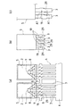
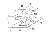
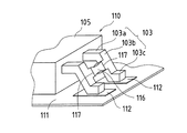
図1は、本発明のリードフレームの一実施例およびこのリードフレームを用いた面実装型半導体装置の製造工程の一例を示す平面図であり、同図(a)はタイバーカット前の状態、同図(b)はタイバーカット後の状態を示している。また、同図(c)はタイバー部分の拡大図である。
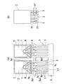
次に、本発明の参考例1について、図3を参照して説明する。
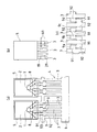
次に、本発明の参考例2について、図4を参照して説明する。
次に、本発明の参考例3について、図5を参照して説明する。
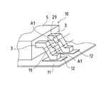
2 載置片
3 リード端子
4 リードフレーム
5 封止樹脂部
6 横枠
8 ボンディングワイヤ
9 タイバー
10 半導体装置
11 回路基板
12 部品ランド
19,29 タイバー根元
9a1,9b1 タイバーの一方の端部(左側端部)
9a2,9b2 タイバーの他方の端部(右側端部)
Claims (3)
- 封止樹脂部より突出した複数のリード端子を備えた面実装型半導体装置用のリードフレームであって、
各リード端子間に架けられた複数のタイバーが、互いに平行に、かつ、リード端子の幅方向に対して傾斜して設けられており、前記タイバーの一端部のリード端子接続位置と他端部のリード端子接続位置とがリード端子の幅方向から見たときに重ならないように、タイバーの傾斜角度が設定されていることを特徴とするリードフレーム。 - 前記請求項1記載のリードフレームを用いて製造されたことを特徴とする面実装型半導体装置。
- 前記請求項2記載の面実装型半導体装置を回路基板上に搭載したことを特徴とする電子機器。
Priority Applications (1)
| Application Number | Priority Date | Filing Date | Title |
|---|---|---|---|
| JP2003422979A JP4137782B2 (ja) | 2003-12-19 | 2003-12-19 | リードフレーム、このリードフレームを用いた面実装型半導体装置およびこの面実装型半導体装置を回路基板上に搭載した電子機器 |
Applications Claiming Priority (1)
| Application Number | Priority Date | Filing Date | Title |
|---|---|---|---|
| JP2003422979A JP4137782B2 (ja) | 2003-12-19 | 2003-12-19 | リードフレーム、このリードフレームを用いた面実装型半導体装置およびこの面実装型半導体装置を回路基板上に搭載した電子機器 |
Publications (2)
| Publication Number | Publication Date |
|---|---|
| JP2005183695A JP2005183695A (ja) | 2005-07-07 |
| JP4137782B2 true JP4137782B2 (ja) | 2008-08-20 |
Family
ID=34783667
Family Applications (1)
| Application Number | Title | Priority Date | Filing Date |
|---|---|---|---|
| JP2003422979A Expired - Fee Related JP4137782B2 (ja) | 2003-12-19 | 2003-12-19 | リードフレーム、このリードフレームを用いた面実装型半導体装置およびこの面実装型半導体装置を回路基板上に搭載した電子機器 |
Country Status (1)
| Country | Link |
|---|---|
| JP (1) | JP4137782B2 (ja) |
Families Citing this family (3)
| Publication number | Priority date | Publication date | Assignee | Title |
|---|---|---|---|---|
| KR101778832B1 (ko) | 2010-11-02 | 2017-09-14 | 다이니폰 인사츠 가부시키가이샤 | Led 소자 탑재용 리드 프레임, 수지 부착 리드 프레임, 반도체 장치의 제조 방법 및 반도체 소자 탑재용 리드 프레임 |
| JP7304830B2 (ja) * | 2020-02-12 | 2023-07-07 | 三菱電機株式会社 | トランスファーモールド型パワーモジュール、リードフレーム、およびトランスファーモールド型パワーモジュールの製造方法 |
| WO2024104166A1 (zh) * | 2022-11-17 | 2024-05-23 | 海信家电集团股份有限公司 | 框架总成、功率模块和设备 |
-
2003
- 2003-12-19 JP JP2003422979A patent/JP4137782B2/ja not_active Expired - Fee Related
Also Published As
| Publication number | Publication date |
|---|---|
| JP2005183695A (ja) | 2005-07-07 |
Similar Documents
| Publication | Publication Date | Title |
|---|---|---|
| US7361983B2 (en) | Semiconductor device and semiconductor assembly module with a gap-controlling lead structure | |
| US6396001B1 (en) | Printed circuit board and method of making the same | |
| JP2000188366A (ja) | 半導体装置 | |
| JP4137782B2 (ja) | リードフレーム、このリードフレームを用いた面実装型半導体装置およびこの面実装型半導体装置を回路基板上に搭載した電子機器 | |
| JP2002334964A (ja) | 半導体装置 | |
| JP2000058739A (ja) | 半導体装置およびその製造に用いるリードフレーム | |
| KR0146063B1 (ko) | 반도체 패키지 및 그 제조방법 | |
| JP2006287131A (ja) | 半導体パッケージ及びその製造方法 | |
| US7345244B2 (en) | Flexible substrate and a connection method thereof that can achieve reliable connection | |
| JPH10256318A (ja) | 半導体装置、その製造方法及びその実装方法、これを実装した回路基板並びにフレキシブル基板及びその製造方法 | |
| JPH07263849A (ja) | 印刷回路基板 | |
| JPH01145630A (ja) | 液晶表示素子 | |
| JP2004235217A (ja) | 半導体装置及び電子装置の製造方法 | |
| JPH06252326A (ja) | 多端子部品、配線基板、多端子部品の実装構造 | |
| JP4961572B2 (ja) | 半導体実装用基板 | |
| JP2570581B2 (ja) | 垂直型表面実装半導体パッケージ | |
| KR100280412B1 (ko) | 버틈 리드 패키지의 표면 실장용 인쇄 회로기판 및 표면 실장방법 | |
| JPH11298125A (ja) | 表面実装用ランド | |
| JP3048236B2 (ja) | 電子部品 | |
| JP3349416B2 (ja) | 電力半導体装置 | |
| JPH07312403A (ja) | 半導体装置及びその製造方法及び実装基板 | |
| JP2006024813A (ja) | プリント基板 | |
| JP4421199B2 (ja) | 半導体装置およびそれを用いた電子機器ならびに半導体装置の製造方法 | |
| JPH06204653A (ja) | 配線基板およびそのはんだ付け方法 | |
| KR0123425B1 (ko) | 절단된 외부 리드를 갖는 반도체 패키지 및 그 실장방법 |
Legal Events
| Date | Code | Title | Description |
|---|---|---|---|
| A621 | Written request for application examination |
Free format text: JAPANESE INTERMEDIATE CODE: A621 Effective date: 20060125 |
|
| A977 | Report on retrieval |
Free format text: JAPANESE INTERMEDIATE CODE: A971007 Effective date: 20080129 |
|
| A131 | Notification of reasons for refusal |
Free format text: JAPANESE INTERMEDIATE CODE: A131 Effective date: 20080205 |
|
| A521 | Request for written amendment filed |
Free format text: JAPANESE INTERMEDIATE CODE: A523 Effective date: 20080407 |
|
| TRDD | Decision of grant or rejection written | ||
| A01 | Written decision to grant a patent or to grant a registration (utility model) |
Free format text: JAPANESE INTERMEDIATE CODE: A01 Effective date: 20080507 |
|
| A01 | Written decision to grant a patent or to grant a registration (utility model) |
Free format text: JAPANESE INTERMEDIATE CODE: A01 |
|
| A61 | First payment of annual fees (during grant procedure) |
Free format text: JAPANESE INTERMEDIATE CODE: A61 Effective date: 20080604 |
|
| R150 | Certificate of patent or registration of utility model |
Free format text: JAPANESE INTERMEDIATE CODE: R150 |
|
| FPAY | Renewal fee payment (event date is renewal date of database) |
Free format text: PAYMENT UNTIL: 20110613 Year of fee payment: 3 |
|
| FPAY | Renewal fee payment (event date is renewal date of database) |
Free format text: PAYMENT UNTIL: 20120613 Year of fee payment: 4 |
|
| FPAY | Renewal fee payment (event date is renewal date of database) |
Free format text: PAYMENT UNTIL: 20120613 Year of fee payment: 4 |
|
| FPAY | Renewal fee payment (event date is renewal date of database) |
Free format text: PAYMENT UNTIL: 20130613 Year of fee payment: 5 |
|
| LAPS | Cancellation because of no payment of annual fees |