JP4133333B2 - Method of processing object and processing apparatus thereof - Google Patents
Method of processing object and processing apparatus thereof Download PDFInfo
- Publication number
- JP4133333B2 JP4133333B2 JP2002564750A JP2002564750A JP4133333B2 JP 4133333 B2 JP4133333 B2 JP 4133333B2 JP 2002564750 A JP2002564750 A JP 2002564750A JP 2002564750 A JP2002564750 A JP 2002564750A JP 4133333 B2 JP4133333 B2 JP 4133333B2
- Authority
- JP
- Japan
- Prior art keywords
- mounting table
- processed
- gas
- processing
- inert gas
- Prior art date
- Legal status (The legal status is an assumption and is not a legal conclusion. Google has not performed a legal analysis and makes no representation as to the accuracy of the status listed.)
- Expired - Lifetime
Links
Images


Classifications
-
- H—ELECTRICITY
- H10—SEMICONDUCTOR DEVICES; ELECTRIC SOLID-STATE DEVICES NOT OTHERWISE PROVIDED FOR
- H10P—GENERIC PROCESSES OR APPARATUS FOR THE MANUFACTURE OR TREATMENT OF DEVICES COVERED BY CLASS H10
- H10P72/00—Handling or holding of wafers, substrates or devices during manufacture or treatment thereof
- H10P72/04—Apparatus for manufacture or treatment
- H10P72/0402—Apparatus for fluid treatment
Landscapes
- Container, Conveyance, Adherence, Positioning, Of Wafer (AREA)
- Drying Of Semiconductors (AREA)
Description
【0001】
【発明の属する技術分野】
この発明は、半導体ウエハ等の被処理体に対して成膜処理やエッチング処理を施す処理方法及びその処理装置に関する。
【0002】
【従来の技術】
半導体装置の製造工程において、例えば、特開平7−321184号公報に示すように、被処理体の表面上に新たな膜を成膜する、または既に積層されている膜をエッチングする処理装置が知られている。
【0003】
この処理装置は、アルミニウム等からなる処理チャンバーを搭載している。この処理チャンバー内には、被処理体を載置し下部電極を兼ねた載置台と、これに対向する上部電極とが設けられている。前記処理装置は、処理チャンバー内を排気により減圧した後、載置台に載置される被処理体を所定の温度に制御しながら、その処理面に処理ガスを吹き付ける。この状態で、上部電極には、例えば60MHz、下部電極(載置台)には13.56MHzの高周波をそれぞれ印加させて処理ガスをプラズマ化し、被処理体に対して所定のエッチング処理を施している。
【0004】
この載置台には、冷却ジャケットが設けられており、載置される被処理体を所望の温度、例えば−100℃まで冷却することができる。さらに、載置台の載置面には複数の伝熱ガス供給孔が開口されている。そして、被処理体を載置した状態で、これらの伝熱ガス供給孔から所望の温度に冷却されたヘリウム(He)等の伝熱ガスを供給して、被処理体への伝熱効率の向上を図っている。
【0005】
また、特開平7−74231号公報に開示されるように、載置台には上下方向に移動する複数のリフターピンが設けられ、被処理体の搬入・搬出時にはそれらのリフターピンが上下することにより、載置台と搬送機構との被処理体の受け渡しを容易にしている。これらのリフターピンは、1つのベースプレートへ一体的に取り付けられており、このベースプレートは、導入機構を介して処理チャンバー外部に取り付けられた上下駆動用エアシリンダの駆動により昇降する。
【0006】
【発明が解決しようとする課題】
しかし、前述した処理チャンバー内には、上下電極の他に、プラズマを集中させるためのフォーカスリング等の金属または非金属部品からなる多数の構成部品が搭載されている。これらの構成部品は、処理チャンバー内に露出している部分がプラズマによって徐々に削れてしまうため、所定期間経過後には交換する必要がある。しかし、生産性の面から見て、メンテナンスにかかる時間や回数を少なくするためには、これらの交換頻度をできるだけ少なくする必要がある。
【0007】
この対策として、フォーカスリング等の構成部品を、削れにくい材質、例えばイットリア(Y203)やジルコニア(ZrO)等の重金属の酸化物によって、製作することが試みられている。その作成方法としては、バルク部品は粉末から焼結したり、アルミニウムを母材とした部品にイットリア(Y203)をコーティング処理したりしている。また、処理チャンバー内面においても、コーティング処理を施してプラズマによる削れを抑制させる部分も設けている。
【0008】
しかしながら、重金属の酸化物によって構成部品を製作したとしてもプラズマに晒していることによって僅かながら削られており、その重金属の微粒子が処理チャンバー内に浮遊している状態が多く見られる。
【0009】
また、重金属の微粒子の周辺にはプラズマから由来している他の気化物が浮遊しているため、この気化物が冷却されると、凝縮して同時に近傍の重金属の微粒子を取り込み、冷却されている部分に付着するという現象が起きる。被処理体を載置する載置台は、前述したように冷却ジャケットで低温度に冷却されているため、被処理体が載置されていないときに露出している載置台の載置面に重金属を含む微粒子が堆積する。
【0010】
その後、新たな被処理体が載置台に載置されると、堆積された重金属を含む微粒子が、その被処理体の裏面に付着して、汚染された被処理体が次の工程に持ち出されるという問題が発生する。
【0011】
本発明は、処理チャンバーの内部に設けられた載置台に被処理体が載置されていないとき、その載置面に重金属を含む微粒子が付着するのを防止し、被処理体が汚染されるのを防止することができる処理方法及び処理装置を提供することを目的とする。
【0012】
【課題を解決するための手段】
本発明は、前記目的を達成するために、減圧雰囲気の処理チャンバー内に設けられた載置台に被処理体を載置した状態で、前記被処理体に所定の処理を施す処理方法において、
前記載置台に被処理体が載置されていないとき、前記載置台上方に不活性ガスを吐出させて、載置面を含む前記載置台を覆うように、加温されたホットガスである前記不活性ガスからなるガス層を形成する被処理体の処理方法を提供する。
また、減圧雰囲気の処理チャンバー内に処理ガスを導入することにより、被処理体に所定の処理を施す処理装置において、前記被処理体を載置するための、前記処理チャンバー内に設けられた載置台と、不活性ガスを前記載置台の載置面へ供給する第1のガス供給孔を有し、前記載置台に前記被処理体が載置されていないとき、前記載置台の載置面を覆うように、加温されたホットガスである不活性ガスのガス層を形成する被処理体の処理装置を提供する。
【0013】
【発明の実施の形態】
以下、図面を参照して本発明の実施形態について詳細に説明する。
【0014】
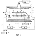
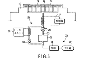
図1は、第1の実施形態における半導体ウエハ等の被処理体へプラズマエッチング処理を施す処理装置の概略的全体構成を示し、図2は処理チャンバー内の載置台の平面構成を示す。また、図3は伝熱ガス供給部及び不活性ガス供給部の概略的構成を示し、図4は、不活性ガス層の形成におけるバルブ開閉について説明するためのタイミングチャートを示している。
【0015】
本実施形態の処理装置本体1には、アルミニウム等の導電性材料からなり、真空状態を維持できるような密閉度を持つ箱状の処理チャンバー2が搭載される。この処理チャンバー2内でプラズマにさらされる内壁面上にはイットリア(Y203)コーティングが施されている。
【0016】
処理チャンバー2内の上面には、上部電極4が設けられ、底部には半導体ウエハ等の被処理体Wを載置する下部電極を兼ねた載置台5が対向して設けられている。上部電極4は、ガス配管を通じてプロセスガス供給部7に接続されており、また処理チャンバー内にガスを吐出するための複数の処理ガス供給孔6が開口されている。載置台5は、処理チャンバー内に露出する表面が例えば、アルマイト処理された凸型円盤形状のアルミニウムからなり、その載置面に被処理体Wが載置される。さらに、載置台5は処理チャンバー2の底部とは絶縁体8を介して固定され、電気的に分離されている。また載置台5内部には給電板9が設けられている。この給電板9は、装置本体1に設置された高周波電源10に接続されており、載置台5に高周波電圧を印加することにより、両電極間にプラズマを発生させるようになっている。この処理チャンバー2内の上部電極4と載置台5との間の空間が被処理体の処理空間3となる。
【0017】
また、載置台5の外周上には、環状のフォーカスリング11が配置されている。このフォーカスリング11は、反応性イオンを被処理体Wに集中させるために使用され、例えばイットリア(Y203)等の重金属の酸化物によって形成されている。さらに、載置面よりも下方の処理チャンバー2の側壁には、チャンバ内を排気するための排気口12が設けられ、排気口12には排気管47及びバルブ48を介して排気系46が接続されている。また、処理チャンバー2の側壁には、被処理体Wを搬入搬出するためのゲート口37が開口され、ゲートバルブ38により開閉される。
【0018】
図2に示すように、載置台5にはリフターピン用の複数の貫通孔13及び伝熱ガスを供給するための複数の伝熱ガス供給孔14が設けられている。これらの伝熱ガス供給孔14は、後述する伝熱ガス供給部15及び不活性ガス供給部16に接続されている。本実施形態では、載置台5上に被処理体Wを保持させるためのチャック部として、静電チャック17を採用しており、載置面上に静電チャック17が設けられている。勿論、被処理体Wを爪などにより機械的に保持するメカニカル・チャックを用いてもよい。
【0019】
前記上部電極4に接続されたプロセスガス供給部7は、例えばC12ガス、C4F6ガス及びBCl3ガスを、図示しない流量制御器(マスフローコントローラ:MFC)やバルブ等を用いて、処理内容に応じて、それぞれ流量制御して上部電極4へ供給する。
【0020】
次に、載置台5に接続された伝熱ガス供給部15及び不活性ガス供給部16について説明する。
【0021】
図3に示すように、伝熱ガス供給部15は、流量と温度が制御されたヘリウムガス(He)等の伝熱ガスを供給するためのガス供給ラインである。このガスラインは、上流(ガス源)側から、伝熱ガスを供給するための伝熱ガス供給源22、ガス流量を制御する流量制御器(MFC)24、一時的にガスをストックするバッファタンク25、供給を遮断するための第1バルブ26a及び温調ユニット27が配置され、これらの間を伝熱ガス供給管23でそれぞれ接続されている。この温調ユニット27は、伝熱ガスを所望の温度まで冷却するための温調部と制御器により構成され、伝熱ガスが所定の温度になるように制御して、伝熱ガス供給孔14へ供給する。伝熱ガスは、被処理体Wの裏面と静電チャック17との間の微小空間に供給されて、載置台5と被処理体Wとの間の伝熱効果を高めている。
【0022】
また、不活性ガス供給部16は、流量と温度が制御された窒素ガス(N2)等の不活性ガスを供給するためのガス供給ラインである。このガスラインは、上流(ガス源)側から、N2ガスを供給するためのN2ガス供給源28、供給を遮断するための第2バルブ26b、ガス流量を制御するMFC29及びヒートアップシステム31が配置され、ガス導入管32によりそれぞれが接続されている。このヒートアップシステム31は、ガス導入管32により伝熱ガス供給管23とバルブ26aとの間に接続している。そして、ヒートアップシステム31は、ヒータ制御システム30に制御されてN2ガスを加温して、伝熱ガス供給管23を経て伝熱ガス供給孔14に供給する。尚、N2ガスは、ヒートアップシステム31によって50℃〜250℃、好ましくは100℃前後に加温され、ホットガスとして載置台5から処理チャンバー2に吹き出される。
【0023】
さらに、載置台5には例えば、4つの孔13が形成されており、各孔内には移動可能に各1本ずつリフターピン33が収納され、これらのリフターピン33は、昇降可能な1つのリフターピン支持機構(図示しない)に固定されて載置面より突き出すように構成されている。勿論、リフターピン33は4本に限定されるものではなく、設計に従って変更可能である。被処理体Wの搬入・搬出時には、4本のリフターピン33によって被処理体Wを載置台5から持ち上げて浮かせた状態で図示しない搬送機構の搬送アームとの受け渡しを行うようになっている。
【0024】
次に、第1の実施形態において、処理装置にプラズマエッチング処理装置を適用した例における処理シーケンスについて説明する。
【0025】
まず、処理チャンバー2内に被処理体Wを搬入する際に、ゲート口37を開口させて被処理体Wを保持する搬送アームを外部(搬送チャンバー等)から処理チャンバー2内へ進入させ載置台5上方で停止させる。その後、リフターピン33を孔13から載置面の上方へ突き出し、被処理体Wを持ち上げて搬送アームから受け取る。
【0026】
搬送アームが退避した後、リフターピン33をスムーズに下降させて、被処理体Wを載置面に載置させると共に、被処理体Wを静電チャック17により載置面に保持させ、それと同時にゲート口37を閉口する。
【0027】
この保持の後、伝熱ガス供給源22からヘリウムガス(He)等の伝熱ガスを流量制御器24で流量制御しつつ流出させて、バッファタンク25及び第1バルブ26aを経て温調ユニット27に流す。温調ユニット27では、伝熱ガスを所定の温度(冷却を行うための温度)になるように制御して、伝熱ガス供給孔14から吐出させる。これにより、伝熱ガスが被処理体Wの裏面と静電チャック17との間の微小空間に供給されることとなり、載置台5と被処理体Wとの伝熱効果が高められる。
【0028】
次に、排気系を駆動させて、排気口12から処理チャンバー2内の気体を排気し、さらに、プロセスガス供給部から所定のプロセスガス、例えば、CF4及び02をそれぞれ300SCCM及び85SCCMずつ処理空間3に供給する。そして、処理チャンバー2内を所定の圧力、例えば350mtorr(46.55Pa)程度に維持させる。
【0029】
次に、高周波電源10から高周波電圧を載置台5へ印加して、上部電極4と載置台5との間の処理空間3内にプラズマを発生させて、被処理体Wのプラズマエッチング処理を行う。そして、プラズマエッチング処理が完了した後、排気系により所定時間で残留ガス等を処理チャンバー2外へ排気する。その際、伝熱ガスとして使用されたHeガスも十分に排気させる。この後、処理チャンバー内の圧力をゲート口を開口してもよい圧力まで調整する。
【0030】
そして、リフターピン33を上昇させて載置台5から被処理体Wを持ち上げて浮かせた状態にする。ゲート口37を開口して、進入してきた搬送アームへ被処理体Wを渡す。搬送アームは、被処理体Wを処理チャンバー2外に搬出し、次に処理を行うための新たな被処理体Wを処理チャンバー2内に搬入する。この新たな被処理体Wは、前回と同様に載置台5に保持される。
【0031】
図4に示すタイミングチャート のように、載置台5に被処理体Wが載置されていないとき、第1バルブ26aは閉として、伝熱ガスの供給を停止する。一方、第2バルブ26bは開けられて、N2ガス供給源28から供給された例えば、流量10SCCM程度のN2ガスが処理チャンバー2内に吐出される。この際、N2ガスは、ヒートアップシステム31によって50℃〜250℃、好ましくは100℃前後に加温されて、ホットガスとして載置面上方に吐出されている。この時、図1に示すように、載置台5(載置面)を覆うように上方に加温されたN2ガスによる不活性ガス層Gが形成される。
【0032】
このN2ガスによる不活性ガス層Gは、処理済みの被処理体Wが載置面を離れてから、次に処理を行う新たな被処理体Wが載置面に保持される直前まで行なわれる。特に、被処理体Wが、離れたり、載置する際に、載置面で位置ずれを起さないように、被処理体W上面側と下面側との気圧差は100mtorr(13.3pa)以下にすることが望ましい。
【0033】
また伝熱ガスと不活性ガス層Gとの関係は、図4に示すように、処理体Wが処理チャンバー2に搬入され、リフターピン33によって載置面に載置される直前に、第1バルブ26aが開けられてHeガスが伝熱ガス供給孔14から被処理体Wの裏面に供給される。このとき、第2バルブ26bが閉じられて、N2ガスの供給は停止される。
【0034】
そして、被処理体Wへの処理が終了して、被処理体Wがリフターピン33によって再び持ち上げられると共に、第2バルブ26bが開けられて、N2ガスの供給が開始される。これと共に、第1バルブ26aは閉じられ、Heガスの供給が停止される。尚、第1バルブ26aを破線で示すように徐々に閉じてもよい。また、MFC24を用いてバッファタンク25へのHeガスの供給を遮断して、バルブ26aをある程度閉じた位置で固定し、バッファタンク25内の残圧でHeガスが伝熱ガス供給孔14に供給されるようにしても、Heガスの供給量を徐々に減ずることもできる。
【0035】
前述したように本発明が解決する問題として、処理チャンバー2内では、プラズマによって削られて発生する重金属の微粒子が浮遊しており、冷却されている部分に付着するという現象が発生していた。
【0036】
以上説明した第1の実施形態では、これを解決するものとして、露出した載置台5(載置面)を覆うように上方に加温されたN2ガスによる不活性ガス層Gを形成したため、載置台5の載置面に重金属の微粒子が付着するのを防止できる。従って、次に処理を行う新たな被処理体Wが載置台5に載置されたときに、その被処理体Wの裏面に重金属の微粒子が付着せず、被処理体Wへの汚染を防止すると共に、次に製造工程への悪影響を防止することができる。また、載置台5の伝熱ガス供給孔14からN2ガスを吹き出しているため、重金属の微粒子が伝熱ガス供給孔14内に進入して、その内壁に付着することも防止できる。
【0037】
次に、第2の実施形態について説明する。
【0038】
図5は、第2実施形態の伝熱ガス供給部及び不活性ガス供給部の概略的構成を示し、図6は、不活性ガス層の形成におけるバルブ開閉について説明するためのタイミングチャートを示している。この第2の実施形態の構成部位において、前述した第1の実施形態と同一構成部位には、同じ参照符号を付してその説明を省略する。
【0039】
本実施形態は、1つのガス供給源と、冷却された伝熱ガスを処理チャンバー内に供給するための主ライン及び加熱された伝熱ガス(第1の実施形態の不活性ガスに相当する)を処理チャンバー内に供給するためバイパスラインとの2ラインにより構成されたガス供給経路を有している。
【0040】
この実施形態では、伝熱ガスを供給する主ラインとして上流(ガス源)側から、He等の伝熱ガス供給源22、流量制御器(MFC)24、バッファタンク25、第1バルブ26a及び温調ユニット27が配置され、それぞれが伝熱ガス供給管23により接続されている。
【0041】
また、MFC24とバッファタンク25の間から、第1バルブ26aと温調ユニット27との間には、バイパスライン35が設けられている。このバイパスライン35には、第2バルブ26b及びヒータユニット36が配置されている。
【0042】
このような構成により、伝熱ガスは、第1バルブ26aが開けられ、第2バルブ26bが閉じられたときは、主ラインを通って伝熱ガス供給孔14に供給され、一方、第1バルブ26aが閉じて、第2バルブ26bが開けられたときは、バイパスライン35を通って伝熱ガス供給孔14に供給される。
【0043】
図6のタイミングチャートに示すように、載置台5に被処理体Wが載置されていないとき、第1バルブ26aは閉じて、第2バルブ26bを開けられる。これらの開閉により、Heガス供給源22からのHeガスは、バイパスライン35を通って、加熱されて載置台5の伝熱ガス供給孔14から処理チャンバー2内へ吐出される。この時、Heガスはヒータユニット36によって、50℃〜250℃、好ましくは100℃前後まで加熱され、ホットガスとして載置台5から処理チャンバー2に吐出され、載置台5の上方に加温されたHeガスによるガス層が形成される。尚、ヒータユニット36は、常時駆動状態となるが、ランプヒータ等の加熱の立ち上がりがよいものを用いて、第2バルブ26bが開となると同時に、ヒータユニット36を駆動させてもよい。
【0044】
従って、前述した第1の実施形態の効果と同等の効果が得られ、重金属の微粒子が載置台5(載置面)へ付着することが防止でき、牽いては被処理体Wへの汚染も防止することができる。
【0045】
また、本実施形態では、Heガスを「伝熱ガス」と「載置台汚染防止のための不活性ガス」の両方に利用しているため、前述した第1の実施形態のように、N2ガス供給源などの不活性ガス供給ラインを別途に設ける必要がなく、構成が簡易化して、装置のコスト的にもメリットがある。
【0046】
次に、第3の実施形態について説明する。
【0047】
図7は、第3の実施形態における半導体ウエハ等の被処理体をプラズマエッチング処理する処理装置の概略的全体構成を示す。この第3の実施形態の構成部位において、前述した第1の実施形態と同一構成部位には、同じ参照符号を付してその説明を省略する。
【0048】
本実施形態は、載置台(下部電極)側だけではなく、載置台と対向する上部電極4側にも不活性ガス供給部22を設けた構成であり、上部電極4及び載置台5の両方から不活性ガスを同時に供給する構成である。
【0049】
この不活性ガス供給部22は、プロセスガス供給部7とバルブ50で構成されるプロセスガス供給ラインに接続しており、バルブ50を経て上部電極4に接続されている。この不活性ガス供給部22は、上流(ガス源)側から、N2等の不活性ガスガス供給源22、MFC19、ヒートアップシステム21及びバルブ49で構成される。ヒートアップシステム21は、ヒータ制御システムにより制御され、N2ガスを加温して上部電極4に供給する。N2ガスはヒートアップシステム21によって50℃〜250℃、好ましくは100℃前後に加温され、ホットガスとして上部電極4から処理チャンバー2内へ吐出される。
【0050】
また、載置台5側における伝熱ガス供給部15、不活性ガス供給部16及び排気系46は、図1及び図3で示した第1の実施形態の構成と同様である。
【0051】
次に、この第3の実施形態の処理装置にプラズマエッチング処理装置を適用した例における処理シーケンスについて説明する。
【0052】
この第3の実施形態は、前述した第1の実施形態と同様に、処理チャンバー2内に被処理体Wを搬入して載置台5に載置した後、被処理体Wに対してエッチング処理を施す。その処理後に、排気系46により処理チャンバー2内の残留ガス等を排気する。排気が完了した後、リフターピン33で被処理体Wを持ち上げ、図示しない搬送アームヘ渡す。
【0053】
処理チャンバー2内から被処理体Wが持ち上げられた時、第1バルブ26aは閉じて、第2バルブ26b及びバルブ49,50が開けられる。これらのバルブ操作により、Heガスの供給は停止され、不活性ガス供給部16、22からそれぞれ加温されたN2ガスが処理チャンバー2内の載置台5及び上部電極4に同時に供給される。
【0054】
載置台5側において、N2ガス供給源28からのN2ガスがMFC29及びヒートアップシステム31により、流量が制限され且つ加温されて、伝熱ガス供給孔14を経て処理チャンバー2内へ吐出されて、載置台5の上方に加温されたN2ガスによる不活性ガス層が形成される。このN2ガスは、ヒートアップシステム31によって、50℃〜250℃、好ましくは100℃前後に加温される。
【0055】
また同時に、上部電極4側においては、N2ガス供給源18からのN2ガスがMFC19、ヒートアップシステム21により、流量が制限され且つ加温されて、上部電極4を経て処理チャンバー2内へ吐出されて、上部電極4の下方に加温されたN2ガスによる不活性ガス層が形成される。このN2ガスは、ヒートアップシステム21によって、50℃〜250℃、好ましくは100℃前後に加温され、ホットガスとして上部電極4から処理チャンバー2に吐出される。
【0056】
以上のような構成により、処理チャンバー2の上方及び下方から所望温度に加温されたN2ガスが処理チャンバー2に供給されて、その内部(処理空間3)の略中間で衝突して周囲に流れるため、処理チャンバー2の内部に浮遊している重金属の微粒子が処理チャンバー2の外周側に押し出される状態となり、またそれぞれにN2ガスによる不活性ガス層が形成されるため、載置台5と上部電極4に重金属の微粒子が付着することを防止できる。
【0057】
従って、載置台5の載置面においては、重金属の微粒子が付着することを防止でき、次に処理を行う新たな被処理体Wが載置台5に載置された時に、その被処理体Wの裏面に付着して被処理体Wを汚染することを防止することができる。また、上部電極においても載置台5に比べて、重金属の微粒子の付着量は少ないがさらに付着しにくくなる。
【0058】
上部電極4の処理ガス供給孔6及び、載置台5の伝熱ガス供給孔14からN2ガスの供給は、双方とも被処理体Wが処理チャンバー2の内部から搬出されてから、次に処理を行うための新たな被処理体Wが搬入されるまで行なわれる。また、載置台5側におけるN2ガスの供給は、被処理体Wが搬入され、リフターピン33が下降して被処理体Wが載置面に載置される直前まで行なわれる。
【0059】
また、図7に示すように処理チャンバー2の内側壁に赤外線ランプ40を設置する。これは、載置台5に被処理体Wが載置されていないときに、不活性ガスの供給とともに、赤外線ランプ40を点灯して載置台5及びその周辺を加温することを併用してもよく、また載置台5に電気ヒータを埋設してもよい。
【0060】
図8は、この第3の実施形態の変形例を示して説明する。
【0061】
ここでは、載置台5に関わる構成のみを示している。
【0062】
この構成は、載置台5を冷却するチラー本体41と、冷却器42とを接続して冷媒を循環する冷媒循環ライン43にバイパス路44及び三方弁45を設けている。この載置台5に被処理体Wが載置されていないときに、三方弁45をバイパス路44に切り換えてチラー本体41から吐出する冷媒を破線矢印で示すようにバイパス路44にバイパスすることにより、載置台5の温度を徐々に上昇させる機能を併用してもよい。
【0063】
また、ホットガスを載置台5の載置面に流す際、特に載置台5の温度が十分低い状態のときには、チラー本体41の動作を止めて、チラー本体41から冷媒が吐出しないようにしてもよい。これにより、チラー本体41から冷媒を吐出させて冷却器42による載置台5の冷却を行う場合に比べて、載置台5の昇温時間を短くすることができ、より迅速に加温されたN2ガスのガス層Gを形成することができるので、スループットの向上、省エネ化という効果がもたらされる。
【0064】
次に、第4の実施形態について説明する。
【0065】
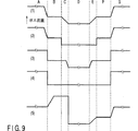
この第4の実施形態は、不活性ガスを供給するタイミングに特徴を持たせたものである。処理チャンバー2内に被処理体Wが搬入されて載置台5上で所定の処理がなされて、真空処理チャンバー外に搬出されるまでの期間は細かく分けると、図9に示す第1例〜第5例のようなパターンとなる。
【0066】
この図9において、横軸は、時間若しくは期間A〜Gを示し、縦軸は、不活性ガスのガス流量を示している。これらの期間においては、
期間Aは、真空処理チャンバーのゲートバルブが開けられ、搬送アームなどの搬送手段によって被処理体が真空処理チャンバーに搬入され始めるまでの期間
期間Bは、被処理体が載置台の真上まで移動される期間
期間Cは、被処理体が載置台に向かって降下させられ、載置台に接するまでの期間
期間Dは、被処理体が載置台に接した状態で所定の処理がなされる期間
期間Eは、被処理体が載置台から離され載置台真上まで上昇させられる期間 期間Fは、被処理体が搬送手段によって処理チャンバー外に搬出され、真空処理チャンバーのゲートバルブが閉められるまでの期間
期間Gは、ゲートバルブが閉められた後の期間
とする。
【0067】
図9の(1)に示す第1例では、期間A及び期間Gで比較的大量の不活性ガスを被処理体表面近傍に供給する。期間B及び期間Fでは比較的少量の不活性ガスを供給する。期間A及び期間Gでは被処理体が処理チャンバー内に無いため、不活性ガスの気流が被処理体の搬送に悪影響を及ぼす心配が無いので比較的大きな流量を選択できるのである。
【0068】
期間Cでは不活性ガスの供給量を徐々に減少させる。期間Dでは熱伝導のためのガス供給のみとする。期間Eでは不活性ガスの供給量を徐々に増加させる。
【0069】
次に図9の(2)に示す第2例では、第1例と比較すれば、期間C及び期間Eにおいて、不活性ガスは吐出させずに、熱伝導ガスのみを吐出させている点が異なっている。期間C及び期間Eでは、被処理体が載置台の真上から下降若しくは上昇しているため、不活性ガスを流すと被処理体の位置ずれが発生する等のおそれがある。しかし、被処理体により載置台上の空間が限られるので、伝熱ガスを吐出させただけでも、重金属の微粒子を含む気流が流入することをある程度防ぐことができる。
【0070】
図9の(3)に示す第3例では、第1例と比較すれば、期間A−B間と期間F−G間の流量の変化が瞬間的に行われる点と、期間Cにおいてその期間の終了直前までの期間Bと実質的に同一量の不活性ガスが供給される点、期間Eの開始直後から期間Fと実質的に同一量の不活性ガスが供給される点が異なる
図9の(4)に示す第4例では、第1例と比較すれば、期間A及び期間Gで不活性ガスが供給され、その他の期間では供給しない点が異なっている。この第4例は、被処理体が処理チャンバーの外にあって、載置台の上方に処理空間ができ、重金属による汚染が最も起きやすい期間にのみ不活性ガスを供給するものである。前述した各例においては、期間DではHeガスなどの伝熱ガスが載置台のガス流路から供給されている。また、不活性ガスが流される期間においては、不活性ガスの流量は期間Dにおける伝熱ガスの流量よりも大きいものとする。載置台表面近傍に供給される不活性ガスの温度は50℃〜250℃が好ましく、100℃前後が最も好ましいものとする。
【0071】
図9の(5)に示す第5例は、載置台温度の平均化を図り、牽いては、被処理体における時間的な温度の均一性を図るものである。
【0072】
この第5例は、期間B、Cにおいて、載置台の真上まで移動され、載置面に搭載されるまでの間に、期間Aの被処理体が無い状態よりも不活性ガスのガス流量を多くして、載置台の温度を一旦上昇させる。そして、期間Dにおいて、不活性ガスの供給を停止し、伝熱ガスのみの供給に切り換える。以降、期間E、F、Gは第1例と同様に、ガス供給を行う。期間Cから期間Dに移行した際に、一旦温度が上昇した載置台が伝熱ガスにより冷却されて温度が低下し、その後、プラズマを発生させるための高周波電力の印加に伴う発熱により温度が上昇するため、載置台はV字形状の温度特性となっている。
【0073】
載置台にこのような温度特性を持たせることにより、載置台に載置された被処理体の温度をより早く所定の温度まで上昇させることができ、また、被処理体の温度を従来と比べてより時間的に均一にすることができる。
【0074】
図10には、前述した実施形態に基づく実験例を示しており、縦軸は載置台に付着する重金属の微粒子の量(イットリア(Y203)の原子数/cm2)であり、横軸のAは従来における載置台へのガスの供給を行なわない例、Bは本発明による載置台に常温のガスを供給した例、Cは本発明による載置台に約100℃に加温されたホットガスを供給した例を示している。イットリウム汚染量の測定は全反射蛍光X線(TXRF)及び気相分解/誘導結合型プラズマ法(VPD/ICP−MS)を用いた。
【0075】
図10に示すように、従来の技術では、載置台5に重金属の微粒子の量は3×10¹²個が付着したのに対して、Bでは、5×10¹⁰個、Cでは、6×10⁹個と百分の一や千分の一となっており、重金属の付着量が大幅に減少したことが解かる。
【0076】
これは、載置台5に被処理体Wが載置されていないときに、伝熱ガス供給孔14からN2ガス等の不活性ガスを供給することにより、載置台5の載置面にガス層(エアカーテン)が形成され、浮遊する重金属の微粒子が侵入して付着することを防止している。さらに、N2ガス等の不活性ガスを加温してホットガスとすることにより、載置台5に重金属の微粒子が侵入しようとしても、ホットガスによって再び蒸発し、さらに重金属の微粒子が侵入するのを防止している。
【0077】
なお、前記各実施形態においては、被処理体をプラズマエッチング処理する処理装置について説明したが、この発明はあらゆる処理装置に適用できる。また、伝熱ガス及び不活性ガスは前記実施形態に限定されるものではなく、適宜変更可能である。
【0078】
【発明の効果】
以上説明したように、この発明によれば、載置台の上部に不活性ガスのガス層を形成することにより、載置台の載置面に重金属の微粒子が付着するのを防止でき、次の被処理体が載置台に載置されたときに被処理体の裏面に転写して被処理体を汚染することを防止することができる。
【0079】
さらに、不活性ガスを加温してホットガスとして吹き出すことにより、重金属の微粒子が載置台に付着しようとしても再び蒸発し、微粒子の付着を防止する効果が大きく、また、載置台の伝熱ガス供給孔から不活性ガスを吹き出すようにすることにより、処理チャンバーの内部に浮遊する重金属の微粒子が伝熱ガス供給孔の内部に付着するのを防止することができる。
【0080】
本発明によれば、被処理体に対して、成膜やエッチングなどの処理を行う処理方法及び処理装置であって、被処理体が載置されていない載置台を覆うように不活性ガスのガス層を形成して、載置台の載置面上への重金属の微粒子の付着を防止し、次に処理を行う新たな被処理体が載置台に載置された際に、その新たな被処理体の裏面へ付着して、被処理体を汚染することを防止することができる。さらに、不活性ガスを加温してホットガスとして載置台の上方に吹き出すことにより、重金属の微粒子が載置台に付着しようとしても再び蒸発させて、微粒子の付着を防止し、また、処理チャンバー内に浮遊する重金属の微粒子が伝熱ガス供給孔の内部に付着することを防止することができる。
【図面の簡単な説明】
【図1】 図1は、本発明の第1の実施形態における処理装置の概略的な構成を示す図である。
【図2】 図2は、第1の実施形態における載置台の平面構成を示す図である。
【図3】 図3は、第1の実施形態における伝熱ガス供給部及び不活性ガス供給部の概略的な構成を示す図である。
【図4】 図4は、第1の実施形態におけるバルブ開閉を説明するためのタイミングチャートである。
【図5】 図5は、本発明の第2の実施形態における伝熱ガス供給部及び不活性ガス供給部の概略的な構成を示す図である。図。
【図6】 図6は、第2の実施形態におけるバルブ開閉を説明するためのタイミングチャートである。
【図7】 図7は、本発明の第3の実施形態における処理装置の概略的な構成を示す図である。図。
【図8】 図8は、本発明による変形例の概略的な構成を示す図である。
【図9】 図9は、本発明の第4の実施形態におけるガス導入パターンを説明するためのタイミングチャートである。
【図10】 図10は、従来技術と本発明による技術を比較した図である。[0001]
BACKGROUND OF THE INVENTION
The present invention relates to a processing method and a processing apparatus for performing a film forming process and an etching process on an object to be processed such as a semiconductor wafer.
[0002]
[Prior art]
In a semiconductor device manufacturing process, for example, as shown in Japanese Patent Laid-Open No. 7-32184, a processing apparatus that forms a new film on the surface of an object to be processed or etches an already laminated film is known. It has been.
[0003]
This processing apparatus is equipped with a processing chamber made of aluminum or the like. In this processing chamber, there are provided a mounting table on which an object to be processed is mounted and also serving as a lower electrode, and an upper electrode facing the mounting table. The processing apparatus depressurizes the inside of the processing chamber by evacuating, and then sprays a processing gas onto the processing surface while controlling the target object mounted on the mounting table at a predetermined temperature. In this state, a high frequency of 60 MHz, for example, is applied to the upper electrode and a high frequency of 13.56 MHz is applied to the lower electrode (mounting table), respectively, so that the processing gas is turned into plasma and a predetermined etching process is performed on the object to be processed. .
[0004]
The mounting table is provided with a cooling jacket, and the object to be mounted can be cooled to a desired temperature, for example, −100 ° C. Further, a plurality of heat transfer gas supply holes are opened on the mounting surface of the mounting table. And in the state which mounted the to-be-processed object, heat transfer gas, such as helium (He) cooled to desired temperature, is supplied from these heat-transfer gas supply holes, and the heat-transfer efficiency to a to-be-processed object is improved. I am trying.
[0005]
Further, as disclosed in Japanese Patent Laid-Open No. 7-74231, the mounting table is provided with a plurality of lifter pins that move in the vertical direction, and when the workpieces are loaded and unloaded, the lifter pins move up and down. Therefore, it is easy to transfer the object to be processed between the mounting table and the transport mechanism. These lifter pins are integrally attached to one base plate, and this base plate is moved up and down by driving an up / down driving air cylinder attached to the outside of the processing chamber via an introduction mechanism.
[0006]
[Problems to be solved by the invention]
However, in addition to the upper and lower electrodes, a large number of components made of metal or non-metal parts such as a focus ring for concentrating plasma are mounted in the processing chamber described above. These components need to be replaced after a lapse of a predetermined period, because the portion exposed in the processing chamber is gradually scraped by the plasma. However, from the viewpoint of productivity, in order to reduce the time and frequency of maintenance, it is necessary to reduce the replacement frequency as much as possible.
[0007]
As a countermeasure, a component such as a focus ring is made of a material that is difficult to cut, such as yttria (Y203) And zirconia (ZrO) and other heavy metal oxides have been tried to manufacture. The bulk parts can be sintered from powder or yttria (Y203) Is coated. In addition, on the inner surface of the processing chamber, there is also provided a portion that performs a coating process and suppresses shaving due to plasma.
[0008]
However, even if the component is made of heavy metal oxide, it is slightly scraped by being exposed to plasma, and there are many cases where the heavy metal fine particles are floating in the processing chamber.
[0009]
In addition, since other vaporized substances derived from plasma are floating around the heavy metal fine particles, when this vaporized substance is cooled, it is condensed and simultaneously takes in the nearby heavy metal fine particles and is cooled. The phenomenon of adhering to the part that occurs. Since the mounting table for mounting the object to be processed is cooled to a low temperature by the cooling jacket as described above, the heavy metal is placed on the mounting surface of the mounting table that is exposed when the object to be processed is not mounted. The fine particles containing are deposited.
[0010]
Thereafter, when a new object to be processed is placed on the mounting table, the deposited fine particles containing heavy metal adhere to the back surface of the object to be processed, and the contaminated object to be processed is taken out to the next step. The problem occurs.
[0011]
In the present invention, when the object to be processed is not mounted on the mounting table provided inside the processing chamber, the particles to be processed are prevented from adhering to the mounting surface and the object to be processed is contaminated. It is an object of the present invention to provide a processing method and a processing apparatus capable of preventing the above-described problem.
[0012]
[Means for Solving the Problems]
In order to achieve the above object, the present invention provides a processing method for performing a predetermined process on a target object in a state where the target object is mounted on a mounting table provided in a processing chamber in a reduced-pressure atmosphere.
When the object to be processed is not placed on the mounting table, the hot gas is heated so as to cover the mounting table including the mounting surface by discharging an inert gas above the mounting table. Provided is a method for processing an object to be processed which forms a gas layer made of an inert gas.
In addition, in a processing apparatus for performing a predetermined process on a target object by introducing a processing gas into the processing chamber in a reduced-pressure atmosphere, a mounting provided in the processing chamber for mounting the target object. A mounting surface, and a first gas supply hole for supplying an inert gas to the mounting surface of the mounting table, and when the object to be processed is not mounted on the mounting table, the mounting surface of the mounting table A processing apparatus for an object to be processed is provided which forms a gas layer of an inert gas which is a heated hot gas so as to cover the substrate.
[0013]
DETAILED DESCRIPTION OF THE INVENTION
Hereinafter, embodiments of the present invention will be described in detail with reference to the drawings.
[0014]
FIG. 1 shows a schematic overall configuration of a processing apparatus for performing a plasma etching process on an object to be processed such as a semiconductor wafer in the first embodiment, and FIG. 2 shows a planar configuration of a mounting table in a processing chamber. 3 shows a schematic configuration of the heat transfer gas supply unit and the inert gas supply unit, and FIG. 4 shows a timing chart for explaining valve opening and closing in the formation of the inert gas layer.
[0015]
The processing apparatus
[0016]
An
[0017]
An
[0018]
As shown in FIG. 2, the mounting table 5 is provided with a plurality of through
[0019]
The process
[0020]
Next, the heat transfer
[0021]
As shown in FIG. 3, the heat transfer
[0022]
Further, the inert
[0023]
Further, for example, four
[0024]
Next, a processing sequence in an example in which a plasma etching processing apparatus is applied to the processing apparatus in the first embodiment will be described.
[0025]
First, when the object to be processed W is carried into the
[0026]
After the transfer arm is retracted, the
[0027]
After this holding, a heat transfer gas such as helium gas (He) is flowed out from the heat transfer
[0028]
Next, the exhaust system is driven to exhaust the gas in the
[0029]
Next, a high-frequency voltage is applied from the high-frequency power source 10 to the mounting table 5 to generate plasma in the
[0030]
Then, the
[0031]
As shown in the timing chart of FIG. 4, when the workpiece W is not placed on the placing table 5, the
[0032]
This N2The inert gas layer G is formed from the gas after the processed object W has left the placement surface until just before the new object W to be processed next is held on the placement surface. In particular, the pressure difference between the upper surface side and the lower surface side of the object to be processed W is 100 mtorr (13.3 pa) so that the object to be processed W is separated or placed so as not to be displaced on the placement surface. The following is desirable.
[0033]
Further, as shown in FIG. 4, the relationship between the heat transfer gas and the inert gas layer G is such that the treatment body W is carried into the
[0034]
Then, the processing on the workpiece W is finished, the workpiece W is lifted again by the
[0035]
As described above, as a problem to be solved by the present invention, in the
[0036]
In the first embodiment described above, as a solution to this problem, N heated upward to cover the exposed mounting table 5 (mounting surface).2Since the inert gas layer G is formed by the gas, it is possible to prevent the heavy metal fine particles from adhering to the mounting surface of the mounting table 5. Therefore, when a new object W to be processed next is placed on the mounting table 5, heavy metal fine particles do not adhere to the back surface of the object W to be prevented from being contaminated. In addition, adverse effects on the manufacturing process can be prevented. Further, N from the heat transfer
[0037]
Next, a second embodiment will be described.
[0038]
FIG. 5 shows a schematic configuration of the heat transfer gas supply unit and the inert gas supply unit of the second embodiment, and FIG. 6 shows a timing chart for explaining valve opening and closing in the formation of the inert gas layer. Yes. In the constituent parts of the second embodiment, the same constituent parts as those of the first embodiment described above are denoted by the same reference numerals, and the description thereof is omitted.
[0039]
In the present embodiment, one gas supply source, a main line for supplying a cooled heat transfer gas into the processing chamber, and a heated heat transfer gas (corresponding to the inert gas of the first embodiment) In order to supply the gas into the processing chamber, a gas supply path constituted by two lines including a bypass line is provided.
[0040]
In this embodiment, the heat transfer
[0041]
A
[0042]
With such a configuration, the heat transfer gas is supplied to the heat transfer
[0043]
As shown in the timing chart of FIG. 6, when the workpiece W is not placed on the placing table 5, the
[0044]
Therefore, an effect equivalent to the effect of the first embodiment described above can be obtained, and heavy metal fine particles can be prevented from adhering to the mounting table 5 (mounting surface). Can be prevented.
[0045]
In this embodiment, since He gas is used for both “heat transfer gas” and “inert gas for preventing contamination of the mounting table”, as in the first embodiment described above, N2There is no need to separately provide an inert gas supply line such as a gas supply source, the configuration is simplified, and there is a merit in terms of cost of the apparatus.
[0046]
Next, a third embodiment will be described.
[0047]
FIG. 7 shows a schematic overall configuration of a processing apparatus for plasma-etching a target object such as a semiconductor wafer in the third embodiment. In the constituent parts of the third embodiment, the same constituent parts as those of the first embodiment described above are denoted by the same reference numerals, and the description thereof is omitted.
[0048]
In the present embodiment, the inert
[0049]
The inert
[0050]
Further, the heat transfer
[0051]
Next, a processing sequence in an example in which a plasma etching processing apparatus is applied to the processing apparatus of the third embodiment will be described.
[0052]
In the third embodiment, similarly to the first embodiment described above, the object to be processed W is loaded into the
[0053]
When the workpiece W is lifted from the
[0054]
On the mounting table 5 side, N2N from
[0055]
At the same time, on the
[0056]
With the above configuration, N heated to a desired temperature from above and below the
[0057]
Accordingly, the heavy metal fine particles can be prevented from adhering to the mounting surface of the mounting table 5, and when the new processing target W to be processed next is mounted on the mounting table 5, the processing target W It is possible to prevent the object W from being adhered to the back surface of the substrate and contaminating it. Also, the amount of heavy metal fine particles attached to the upper electrode is smaller than that of the mounting table 5, but it is more difficult to attach.
[0058]
N from the processing gas supply hole 6 of the
[0059]
In addition, as shown in FIG. 7, an
[0060]
FIG. 8 shows and describes a modification of the third embodiment.
[0061]
Here, only the configuration related to the mounting table 5 is shown.
[0062]
In this configuration, a bypass path 44 and a three-
[0063]
Further, when the hot gas is allowed to flow on the mounting surface of the mounting table 5, especially when the temperature of the mounting table 5 is sufficiently low, the operation of the
[0064]
Next, a fourth embodiment will be described.
[0065]
The fourth embodiment is characterized by the timing of supplying the inert gas. When the target object W is carried into the
[0066]
In FIG. 9, the horizontal axis indicates time or periods A to G, and the vertical axis indicates the gas flow rate of the inert gas. During these periods,
Period A is a period from when the gate valve of the vacuum processing chamber is opened until the object to be processed is transferred into the vacuum processing chamber by the transfer means such as the transfer arm.
Period B is a period during which the object to be processed is moved to just above the mounting table.
Period C is a period from when the workpiece is lowered toward the mounting table until it comes into contact with the mounting table.
The period D is a period during which a predetermined process is performed in a state where the object to be processed is in contact with the mounting table.
Period E is a period in which the object to be processed is separated from the mounting table and raised to just above the mounting table. Period F is until the object to be processed is carried out of the processing chamber by the transfer means and the gate valve of the vacuum processing chamber is closed. Period of
Period G is the period after the gate valve is closed
And
[0067]
In the first example shown in (1) of FIG. 9, a relatively large amount of inert gas is supplied to the vicinity of the surface of the object to be processed in the period A and the period G. In the period B and the period F, a relatively small amount of inert gas is supplied. In the period A and the period G, since the object to be processed is not in the processing chamber, there is no concern that the flow of the inert gas adversely affects the conveyance of the object to be processed, so that a relatively large flow rate can be selected.
[0068]
In period C, the supply amount of the inert gas is gradually decreased. In period D, only gas supply for heat conduction is performed. In period E, the supply amount of the inert gas is gradually increased.
[0069]
Next, in the second example shown in (2) of FIG. 9, as compared with the first example, in the period C and the period E, only the heat conduction gas is discharged without discharging the inert gas. Is different. In the period C and the period E, the object to be processed descends or rises from directly above the mounting table, and therefore there is a possibility that the position of the object to be processed may be shifted when an inert gas is flowed. However, since the space on the mounting table is limited by the object to be processed, it is possible to prevent airflow including heavy metal fine particles from flowing in to some extent just by discharging the heat transfer gas.
[0070]
In the third example shown in (3) of FIG. 9, compared to the first example, the change in the flow rate between the periods A and B and the period FG is instantaneously performed, and in the period C, the period The point is that substantially the same amount of the inert gas is supplied as in the period B until immediately before the end of the period E, and the point that the inert gas substantially the same amount as in the period F is supplied immediately after the start of the period E.
The fourth example shown in (4) of FIG. 9 is different from the first example in that the inert gas is supplied in the period A and the period G and not supplied in the other periods. In the fourth example, an inert gas is supplied only during a period in which the object to be processed is outside the processing chamber, a processing space is formed above the mounting table, and contamination with heavy metal is most likely to occur. In each example described above, in period D, heat transfer gas such as He gas is supplied from the gas flow path of the mounting table. Further, it is assumed that the flow rate of the inert gas is larger than the flow rate of the heat transfer gas in the period D during the period in which the inert gas flows. The temperature of the inert gas supplied in the vicinity of the surface of the mounting table is preferably 50 ° C to 250 ° C, and most preferably around 100 ° C.
[0071]
In the fifth example shown in (5) of FIG. 9, the temperature of the mounting table is averaged, and in order to achieve uniformity of temperature in the object to be processed.
[0072]
In the fifth example, in the periods B and C, the gas flow rate of the inert gas is higher than the state in which there is no object to be processed in the period A, until it is moved to just above the mounting table and mounted on the mounting surface. To increase the temperature of the mounting table. In period D, the supply of the inert gas is stopped and the supply is switched to the supply of only the heat transfer gas. Thereafter, during the periods E, F, and G, gas supply is performed as in the first example. When the period C is shifted to the period D, the mounting table whose temperature is once increased is cooled by the heat transfer gas, and the temperature is decreased. Thereafter, the temperature is increased due to heat generated by the application of high-frequency power for generating plasma. Therefore, the mounting table has a V-shaped temperature characteristic.
[0073]
By giving such a temperature characteristic to the mounting table, the temperature of the object to be processed placed on the mounting table can be raised to a predetermined temperature more quickly, and the temperature of the object to be processed is compared with the conventional one. More uniform in time.
[0074]
FIG. 10 shows an experimental example based on the above-described embodiment, and the vertical axis represents the amount of heavy metal fine particles adhering to the mounting table (yttria (Y203), The horizontal axis A is an example in which gas is not supplied to the conventional mounting table, B is an example in which normal temperature gas is supplied to the mounting table according to the present invention, and C is according to the present invention. The example which supplied the hot gas heated at about 100 degreeC to the mounting base is shown. The amount of yttrium contamination was measured by total reflection X-ray fluorescence (TXRF) and gas phase decomposition / inductively coupled plasma method (VPD / ICP-MS).
[0075]
As shown in FIG. 10, in the conventional technique, the amount of heavy metal fine particles on the mounting table 5 is 3 × 10.12In the case of B, 5 × 10106 x 10 for C9It can be seen that the amount of heavy metals attached has decreased significantly, with one-hundredth and one-thousandth.
[0076]
This is because when the workpiece W is not placed on the placing table 5, N is transferred from the heat transfer gas supply hole 14.2By supplying an inert gas such as a gas, a gas layer (air curtain) is formed on the mounting surface of the mounting table 5 to prevent floating heavy metal fine particles from entering and adhering. In addition, N2By heating an inert gas such as a gas to form a hot gas, even if heavy metal fine particles try to penetrate into the mounting table 5, they are evaporated again by the hot gas, and further prevent heavy metal fine particles from entering. Yes.
[0077]
In each of the above embodiments, the processing apparatus for performing the plasma etching process on the object to be processed has been described. However, the present invention can be applied to any processing apparatus. Further, the heat transfer gas and the inert gas are not limited to the above embodiment, and can be changed as appropriate.
[0078]
【The invention's effect】
As described above, according to the present invention, by forming a gas layer of an inert gas on the mounting table, it is possible to prevent heavy metal fine particles from adhering to the mounting surface of the mounting table. When the processing body is placed on the mounting table, it can be prevented that the processing body is contaminated by being transferred to the back surface of the processing body.
[0079]
Furthermore, by heating the inert gas and blowing it out as a hot gas, heavy metal fine particles are vaporized again even if they try to adhere to the mounting table, and the effect of preventing the adhesion of the fine particles is great. By blowing out the inert gas from the supply hole, it is possible to prevent fine particles of heavy metal floating inside the processing chamber from adhering to the inside of the heat transfer gas supply hole.
[0080]
According to the present invention, there is provided a processing method and a processing apparatus for performing processing such as film formation and etching on an object to be processed, the inert gas being formed so as to cover a mounting table on which the object to be processed is not mounted. A gas layer is formed to prevent the deposition of heavy metal fine particles on the mounting surface of the mounting table, and when a new object to be processed next is mounted on the mounting table, the new object It is possible to prevent the object to be processed from being adhered to the back surface of the object to be processed. Further, by heating the inert gas and blowing it out as a hot gas above the mounting table, even if heavy metal particles try to adhere to the mounting table, they are evaporated again, preventing the adhesion of the particles, and also in the processing chamber. It is possible to prevent the heavy metal fine particles floating on the inside from adhering to the inside of the heat transfer gas supply hole.
[Brief description of the drawings]
FIG. 1 is a diagram showing a schematic configuration of a processing apparatus according to a first embodiment of the present invention.
FIG. 2 is a diagram illustrating a planar configuration of the mounting table in the first embodiment.
FIG. 3 is a diagram showing a schematic configuration of a heat transfer gas supply unit and an inert gas supply unit in the first embodiment.
FIG. 4 is a timing chart for explaining valve opening and closing in the first embodiment.
FIG. 5 is a diagram showing a schematic configuration of a heat transfer gas supply unit and an inert gas supply unit in a second embodiment of the present invention. Figure.
FIG. 6 is a timing chart for explaining valve opening and closing in the second embodiment.
FIG. 7 is a diagram showing a schematic configuration of a processing apparatus according to a third embodiment of the present invention. Figure.
FIG. 8 is a diagram showing a schematic configuration of a modification according to the present invention.
FIG. 9 is a timing chart for explaining a gas introduction pattern in the fourth embodiment of the present invention.
FIG. 10 is a diagram comparing the prior art and the technique according to the present invention.
Claims (28)
前記載置台に被処理体が載置されていないとき、前記載置台上方に不活性ガスを吐出させて、載置面を含む前記載置台を覆うように、加温されたホットガスである前記不活性ガスからなるガス層を形成することを特徴とする被処理体の処理方法。In a processing method of performing a predetermined process on the target object in a state where the target object is mounted on a mounting table provided in a processing chamber in a reduced-pressure atmosphere,
When the object to be processed is not placed on the mounting table, the hot gas is heated so as to cover the mounting table including the mounting surface by discharging an inert gas above the mounting table. A processing method for an object to be processed, wherein a gas layer made of an inert gas is formed.
前記載置台に被処理体が載置されていないとき、前記載置台上方に不活性ガスを吐出させ、且つ前記処理チャンバー内で前記載置台と対向する上部電極から加温されたホットガスである不活性ガスを吐出させることを特徴とする被処理体の処理方法。In a processing method of performing a predetermined process on the target object in a state where the target object is mounted on a mounting table provided in a processing chamber in a reduced-pressure atmosphere,
When the object to be processed is not mounted on the mounting table, the hot gas is discharged from the upper electrode facing the mounting table in the processing chamber by discharging an inert gas above the mounting table. A processing method of an object to be processed, characterized by discharging an inert gas.
b)前記載置台表面に前記被処理体を置く工程と、
c)第一の温度に制御された前記載置台表面に前記被処理体を置いた状態で、前記載置台に設けられたガス流路を通して前記載置台表面と被処理体との間の微小空間にガスを供給しながら前記被処理体表面をプラズマ雰囲気で処理する工程と、
d)前記被処理体を前記載置台表面から上方へ離す工程と、
e)前記被処理体を前記載置台の上方から前記処理チャンバー外に搬出する工程と、を有するプラズマ処理方法であって、
少なくとも工程a)及び工程e)の期間中、前記第一の温度よりも高温な不活性ガスを前記載置台表面近傍に供給することを特徴とする被処理体の処理方法。 a) carrying the object into a processing chamber that can be maintained in a reduced-pressure atmosphere and moving the object above a mounting table provided in the processing chamber;
b) placing the object to be treated on the table surface;
c) A minute space between the surface of the mounting table and the object to be processed through the gas flow path provided in the mounting table in a state where the object to be processed is placed on the surface of the mounting table controlled to the first temperature. Processing the surface of the object to be processed in a plasma atmosphere while supplying gas to
d) separating the object to be processed upward from the mounting table surface;
e) carrying out the object to be processed out of the processing chamber from above the mounting table, and a plasma processing method comprising:
A processing method for an object to be processed, wherein an inert gas having a temperature higher than the first temperature is supplied to the vicinity of the surface of the mounting table at least during the period of step a) and step e).
前記工程d)における前記載置台表面から前記被処理体が離れた直後以降の期間と、において、
前記不活性ガスを前記載置台表面近傍に供給することを特徴とする請求項7に記載の被処理体の処理方法。A period until immediately before the object to be processed is placed on the mounting table surface in the step b),
In the period immediately after the workpiece is separated from the mounting table surface in the step d),
The method for processing an object to be processed according to claim 7, wherein the inert gas is supplied to the vicinity of the surface of the mounting table.
前記載置台の前記ガス流路を通して供給されると共に、前記不活性ガスの流量は前記工程c)における伝熱ガスの流量よりも大であることを特徴とする請求項7に記載の被処理体の処理方法。The inert gas is
The object to be processed according to claim 7, wherein the workpiece is supplied through the gas flow path of the mounting table, and the flow rate of the inert gas is larger than the flow rate of the heat transfer gas in the step c). Processing method.
上記被処理体を移動させる前記工程a)及び工程e)の期間に、前記載置台表面近傍に実質的に重金属の粒子を含まない不活性ガスを、前記工程b)〜工程d)に流す第1の流量よりも大なる第2の流量で供給することを特徴とする請求項7記載の被処理体の処理方法。In the period from step a) to step e),
In the period of the step a) and the step e) for moving the object to be processed, an inert gas substantially free of heavy metal particles in the vicinity of the mounting table surface is passed through the steps b) to d). 8. The processing method for an object to be processed according to claim 7, wherein the second flow rate is higher than the first flow rate.
前記処理チャンバー内の電極から不活性ガスを供給する工程と、
ガス源と前記電極間に設けられたバイパス回路を経由して前記電極から加温された不活性ガスを供給する工程と、
を交互に行うことを特徴とする被処理体の処理方法。The object to be processed is loaded into a processing chamber that can be maintained in a reduced-pressure atmosphere, placed on a mounting table provided in the processing chamber and subjected to a predetermined process, and then the object to be processed is unloaded from the processing chamber. In the processing method of repeatedly processing to perform processing on a plurality of objects to be processed,
Supplying an inert gas from an electrode in the processing chamber;
Supplying a heated inert gas from the electrode via a bypass circuit provided between a gas source and the electrode;
A method for processing an object to be processed, characterized in that:
前記不活性ガスは前記バイパス回路に設けられたヒータユニットにより加温されることを特徴とする請求項13に記載の被処理体の処理方法。Supplying the warmed inert gas;
The method for processing an object to be processed according to claim 13 , wherein the inert gas is heated by a heater unit provided in the bypass circuit.
ガス源と前記電極間に設けられたバイパス回路を経由して前記電極から加温された不活性ガスを供給する工程と、
を切り換えることを特徴とする請求項13に記載の被処理体の処理方法。Supplying an inert gas from an electrode in the processing chamber when the object to be processed is not placed on the mounting table;
Supplying a heated inert gas from the electrode via a bypass circuit provided between a gas source and the electrode;
The method for processing an object to be processed according to claim 13 , wherein:
前記載置台に被処理体が載置されていないときに、前記チャンバー内に設けられた前記ガス供給孔の周辺部上又は/及び、該ガス供給孔から供給されたガスが滞留又は通過する該チャンバー内に配置される構成部材上に、加温されたホットガスである前記不活性ガスからなるガス層を形成することを特徴とする被処理体の処理方法。The object to be processed is carried into a processing chamber that can be maintained in a reduced pressure atmosphere, placed on a mounting table provided in the processing chamber, and subjected to predetermined processing in an atmosphere containing gas supplied from the gas supply hole. In a processing method for performing processing on a plurality of objects to be processed by repeatedly carrying out the object to be processed out of the processing chamber after the application,
When the object to be processed is not placed on the mounting table, the gas supplied from the gas supply hole stays or passes on or around the gas supply hole provided in the chamber. A processing method for an object to be processed, comprising: forming a gas layer made of the inert gas which is a heated hot gas on a constituent member disposed in a chamber.
前記被処理体を載置するための、前記処理チャンバー内に設けられた載置台と、不活性ガスを前記載置台の載置面へ供給する第1のガス供給孔を有し、A mounting table provided in the processing chamber for mounting the object to be processed; and a first gas supply hole for supplying an inert gas to the mounting surface of the mounting table.
前記載置台に被処理体が載置されていないとき、前記載置台上方に不活性ガスを吐出させ、且つ前記処理チャンバー内で前記載置台と対向する上部電極から加温されたホットガスである不活性ガスを吐出させることを特徴とする被処理体の処理装置。When the object to be processed is not mounted on the mounting table, the hot gas is discharged from the upper electrode facing the mounting table in the processing chamber by discharging an inert gas above the mounting table. A processing apparatus for an object to be processed, wherein an inert gas is discharged.
前記第2の不活性ガス供給源から前記第2のガス供給孔までの間にヒータを設けたことを特徴とする請求項17又は18に記載の被処理体の処理装置。The apparatus for processing an object to be processed according to claim 17 or 18, wherein a heater is provided between the second inert gas supply source and the second gas supply hole.
前記被処理体を載置するための、前記処理チャンバー内に設けられた載置台と、不活性ガスを前記載置台の載置面へ供給する第1のガス供給孔を有し、前記載置台に前記被処理体が載置されていないとき、前記載置台の載置面を覆うように、加温されたホットガスである不活性ガスのガス層を形成することを特徴とする被処理体の処理装置。In a processing apparatus for performing a predetermined process on a target object by introducing a processing gas into a processing chamber in a reduced-pressure atmosphere,
A mounting table for mounting the object to be processed; a mounting table provided in the processing chamber; and a first gas supply hole for supplying an inert gas to the mounting surface of the mounting table. When the object to be processed is not placed on the substrate, a gas layer of an inert gas that is a heated hot gas is formed so as to cover the placement surface of the mounting table. Processing equipment.
前記伝熱ガスの供給源であることを特徴とする請求項20に記載の被処理体の処理装置。The first inert gas supply source for supplying the inert gas is:
21. The processing apparatus for an object to be processed according to claim 20 , which is a supply source of the heat transfer gas.
Applications Claiming Priority (3)
| Application Number | Priority Date | Filing Date | Title |
|---|---|---|---|
| JP2001038610 | 2001-02-15 | ||
| JP2001038610 | 2001-02-15 | ||
| PCT/JP2002/001279 WO2002065532A1 (en) | 2001-02-15 | 2002-02-15 | Work treating method and treating device |
Publications (2)
| Publication Number | Publication Date |
|---|---|
| JPWO2002065532A1 JPWO2002065532A1 (en) | 2004-06-17 |
| JP4133333B2 true JP4133333B2 (en) | 2008-08-13 |
Family
ID=18901552
Family Applications (1)
| Application Number | Title | Priority Date | Filing Date |
|---|---|---|---|
| JP2002564750A Expired - Lifetime JP4133333B2 (en) | 2001-02-15 | 2002-02-15 | Method of processing object and processing apparatus thereof |
Country Status (4)
| Country | Link |
|---|---|
| US (2) | US7615259B2 (en) |
| JP (1) | JP4133333B2 (en) |
| CN (2) | CN101038863B (en) |
| WO (1) | WO2002065532A1 (en) |
Cited By (1)
| Publication number | Priority date | Publication date | Assignee | Title |
|---|---|---|---|---|
| JP2020120081A (en) * | 2019-01-28 | 2020-08-06 | 東京エレクトロン株式会社 | Substrate processing apparatus |
Families Citing this family (295)
| Publication number | Priority date | Publication date | Assignee | Title |
|---|---|---|---|---|
| CN101038863B (en) * | 2001-02-15 | 2011-07-06 | 东京毅力科创株式会社 | Method and apparatus for processing workpiece |
| US7390755B1 (en) | 2002-03-26 | 2008-06-24 | Novellus Systems, Inc. | Methods for post etch cleans |
| US20040261946A1 (en) | 2003-04-24 | 2004-12-30 | Tokyo Electron Limited | Plasma processing apparatus, focus ring, and susceptor |
| US7853477B2 (en) | 2003-12-30 | 2010-12-14 | O'shea Michael D | RF-based electronic system and method for automatic cross-marketing promotional offers and check-outs |
| US7288484B1 (en) | 2004-07-13 | 2007-10-30 | Novellus Systems, Inc. | Photoresist strip method for low-k dielectrics |
| US7532310B2 (en) * | 2004-10-22 | 2009-05-12 | Asml Netherlands B.V. | Apparatus, method for supporting and/or thermally conditioning a substrate, a support table, and a chuck |
| US8193096B2 (en) * | 2004-12-13 | 2012-06-05 | Novellus Systems, Inc. | High dose implantation strip (HDIS) in H2 base chemistry |
| JP4486489B2 (en) * | 2004-12-22 | 2010-06-23 | 東京エレクトロン株式会社 | Processing method and processing apparatus |
| US8129281B1 (en) | 2005-05-12 | 2012-03-06 | Novellus Systems, Inc. | Plasma based photoresist removal system for cleaning post ash residue |
| JP4804968B2 (en) * | 2006-03-16 | 2011-11-02 | 株式会社日立ハイテクノロジーズ | Plasma processing equipment |
| US7718032B2 (en) * | 2006-06-22 | 2010-05-18 | Tokyo Electron Limited | Dry non-plasma treatment system and method of using |
| JP5138195B2 (en) * | 2006-09-26 | 2013-02-06 | 東京エレクトロン株式会社 | Heat transfer gas supply mechanism, heat transfer gas supply method, substrate processing apparatus, and substrate processing method |
| US7740768B1 (en) | 2006-10-12 | 2010-06-22 | Novellus Systems, Inc. | Simultaneous front side ash and backside clean |
| KR101312292B1 (en) * | 2006-12-11 | 2013-09-27 | 엘아이지에이디피 주식회사 | Device of preventing substrate of plasma processing apparatus from breakdown and method of thereof |
| US8435895B2 (en) * | 2007-04-04 | 2013-05-07 | Novellus Systems, Inc. | Methods for stripping photoresist and/or cleaning metal regions |
| KR101432562B1 (en) * | 2007-12-31 | 2014-08-21 | (주)소슬 | Substrate processing apparatus and substrate processing method |
| US8591661B2 (en) | 2009-12-11 | 2013-11-26 | Novellus Systems, Inc. | Low damage photoresist strip method for low-K dielectrics |
| CN101758420B (en) * | 2008-12-08 | 2016-04-20 | 香港科技大学 | A system, apparatus and method for providing cooling |
| US20110143548A1 (en) | 2009-12-11 | 2011-06-16 | David Cheung | Ultra low silicon loss high dose implant strip |
| WO2011072061A2 (en) * | 2009-12-11 | 2011-06-16 | Novellus Systems, Inc. | Enhanced passivation process to protect silicon prior to high dose implant strip |
| CN102194651B (en) * | 2010-03-12 | 2013-03-27 | 中芯国际集成电路制造(上海)有限公司 | Loading cavity of semiconductor film-forming device |
| US8866271B2 (en) * | 2010-10-07 | 2014-10-21 | Hitachi Kokusai Electric Inc. | Semiconductor device manufacturing method, substrate processing apparatus and semiconductor device |
| JP6203476B2 (en) * | 2011-03-08 | 2017-09-27 | 東京エレクトロン株式会社 | Substrate temperature control method and plasma processing apparatus |
| US20130023129A1 (en) | 2011-07-20 | 2013-01-24 | Asm America, Inc. | Pressure transmitter for a semiconductor processing environment |
| WO2013022669A2 (en) | 2011-08-05 | 2013-02-14 | 3M Innovative Properties Company | Systems and methods for processing vapor |
| US9613825B2 (en) | 2011-08-26 | 2017-04-04 | Novellus Systems, Inc. | Photoresist strip processes for improved device integrity |
| US10714315B2 (en) | 2012-10-12 | 2020-07-14 | Asm Ip Holdings B.V. | Semiconductor reaction chamber showerhead |
| JP6100564B2 (en) * | 2013-01-24 | 2017-03-22 | 東京エレクトロン株式会社 | Substrate processing apparatus and mounting table |
| US20160376700A1 (en) | 2013-02-01 | 2016-12-29 | Asm Ip Holding B.V. | System for treatment of deposition reactor |
| JP5859583B2 (en) * | 2014-01-30 | 2016-02-10 | 株式会社日立国際電気 | Substrate processing apparatus and semiconductor device manufacturing method |
| US9514954B2 (en) | 2014-06-10 | 2016-12-06 | Lam Research Corporation | Peroxide-vapor treatment for enhancing photoresist-strip performance and modifying organic films |
| US10858737B2 (en) | 2014-07-28 | 2020-12-08 | Asm Ip Holding B.V. | Showerhead assembly and components thereof |
| US10941490B2 (en) | 2014-10-07 | 2021-03-09 | Asm Ip Holding B.V. | Multiple temperature range susceptor, assembly, reactor and system including the susceptor, and methods of using the same |
| US10276355B2 (en) | 2015-03-12 | 2019-04-30 | Asm Ip Holding B.V. | Multi-zone reactor, system including the reactor, and method of using the same |
| US10458018B2 (en) | 2015-06-26 | 2019-10-29 | Asm Ip Holding B.V. | Structures including metal carbide material, devices including the structures, and methods of forming same |
| US10211308B2 (en) | 2015-10-21 | 2019-02-19 | Asm Ip Holding B.V. | NbMC layers |
| US11139308B2 (en) | 2015-12-29 | 2021-10-05 | Asm Ip Holding B.V. | Atomic layer deposition of III-V compounds to form V-NAND devices |
| US10529554B2 (en) | 2016-02-19 | 2020-01-07 | Asm Ip Holding B.V. | Method for forming silicon nitride film selectively on sidewalls or flat surfaces of trenches |
| US10343920B2 (en) | 2016-03-18 | 2019-07-09 | Asm Ip Holding B.V. | Aligned carbon nanotubes |
| CN108293292B (en) * | 2016-03-30 | 2020-08-18 | 东京毅力科创株式会社 | Plasma electrode and plasma processing apparatus |
| US11453943B2 (en) | 2016-05-25 | 2022-09-27 | Asm Ip Holding B.V. | Method for forming carbon-containing silicon/metal oxide or nitride film by ALD using silicon precursor and hydrocarbon precursor |
| US9859151B1 (en) | 2016-07-08 | 2018-01-02 | Asm Ip Holding B.V. | Selective film deposition method to form air gaps |
| US10612137B2 (en) | 2016-07-08 | 2020-04-07 | Asm Ip Holdings B.V. | Organic reactants for atomic layer deposition |
| US9812320B1 (en) | 2016-07-28 | 2017-11-07 | Asm Ip Holding B.V. | Method and apparatus for filling a gap |
| US9887082B1 (en) | 2016-07-28 | 2018-02-06 | Asm Ip Holding B.V. | Method and apparatus for filling a gap |
| US11532757B2 (en) | 2016-10-27 | 2022-12-20 | Asm Ip Holding B.V. | Deposition of charge trapping layers |
| US10714350B2 (en) | 2016-11-01 | 2020-07-14 | ASM IP Holdings, B.V. | Methods for forming a transition metal niobium nitride film on a substrate by atomic layer deposition and related semiconductor device structures |
| KR102546317B1 (en) | 2016-11-15 | 2023-06-21 | 에이에스엠 아이피 홀딩 비.브이. | Gas supply unit and substrate processing apparatus including the same |
| CN106531666A (en) * | 2016-11-22 | 2017-03-22 | 上海华力微电子有限公司 | Process chamber and semiconductor process apparatus |
| JP2018095916A (en) * | 2016-12-13 | 2018-06-21 | 株式会社日立国際電気 | Substrate treatment apparatus, lithography temperature manufacturing method, program |
| KR102762543B1 (en) | 2016-12-14 | 2025-02-05 | 에이에스엠 아이피 홀딩 비.브이. | Substrate processing apparatus |
| US11581186B2 (en) | 2016-12-15 | 2023-02-14 | Asm Ip Holding B.V. | Sequential infiltration synthesis apparatus |
| US11447861B2 (en) | 2016-12-15 | 2022-09-20 | Asm Ip Holding B.V. | Sequential infiltration synthesis apparatus and a method of forming a patterned structure |
| US10269558B2 (en) | 2016-12-22 | 2019-04-23 | Asm Ip Holding B.V. | Method of forming a structure on a substrate |
| US11390950B2 (en) | 2017-01-10 | 2022-07-19 | Asm Ip Holding B.V. | Reactor system and method to reduce residue buildup during a film deposition process |
| US10468261B2 (en) | 2017-02-15 | 2019-11-05 | Asm Ip Holding B.V. | Methods for forming a metallic film on a substrate by cyclical deposition and related semiconductor device structures |
| US10770286B2 (en) | 2017-05-08 | 2020-09-08 | Asm Ip Holdings B.V. | Methods for selectively forming a silicon nitride film on a substrate and related semiconductor device structures |
| CN108987323B (en) * | 2017-06-05 | 2020-03-31 | 北京北方华创微电子装备有限公司 | Bearing device and semiconductor processing equipment |
| US12040200B2 (en) | 2017-06-20 | 2024-07-16 | Asm Ip Holding B.V. | Semiconductor processing apparatus and methods for calibrating a semiconductor processing apparatus |
| US11306395B2 (en) | 2017-06-28 | 2022-04-19 | Asm Ip Holding B.V. | Methods for depositing a transition metal nitride film on a substrate by atomic layer deposition and related deposition apparatus |
| KR20190009245A (en) | 2017-07-18 | 2019-01-28 | 에이에스엠 아이피 홀딩 비.브이. | Methods for forming a semiconductor device structure and related semiconductor device structures |
| US11374112B2 (en) | 2017-07-19 | 2022-06-28 | Asm Ip Holding B.V. | Method for depositing a group IV semiconductor and related semiconductor device structures |
| US10590535B2 (en) | 2017-07-26 | 2020-03-17 | Asm Ip Holdings B.V. | Chemical treatment, deposition and/or infiltration apparatus and method for using the same |
| TWI815813B (en) | 2017-08-04 | 2023-09-21 | 荷蘭商Asm智慧財產控股公司 | Showerhead assembly for distributing a gas within a reaction chamber |
| US10770336B2 (en) | 2017-08-08 | 2020-09-08 | Asm Ip Holding B.V. | Substrate lift mechanism and reactor including same |
| US10692741B2 (en) | 2017-08-08 | 2020-06-23 | Asm Ip Holdings B.V. | Radiation shield |
| US11769682B2 (en) | 2017-08-09 | 2023-09-26 | Asm Ip Holding B.V. | Storage apparatus for storing cassettes for substrates and processing apparatus equipped therewith |
| US11830730B2 (en) | 2017-08-29 | 2023-11-28 | Asm Ip Holding B.V. | Layer forming method and apparatus |
| US11295980B2 (en) | 2017-08-30 | 2022-04-05 | Asm Ip Holding B.V. | Methods for depositing a molybdenum metal film over a dielectric surface of a substrate by a cyclical deposition process and related semiconductor device structures |
| US10658205B2 (en) | 2017-09-28 | 2020-05-19 | Asm Ip Holdings B.V. | Chemical dispensing apparatus and methods for dispensing a chemical to a reaction chamber |
| US10403504B2 (en) | 2017-10-05 | 2019-09-03 | Asm Ip Holding B.V. | Method for selectively depositing a metallic film on a substrate |
| US10923344B2 (en) | 2017-10-30 | 2021-02-16 | Asm Ip Holding B.V. | Methods for forming a semiconductor structure and related semiconductor structures |
| US10732615B2 (en) | 2017-10-30 | 2020-08-04 | Varian Semiconductor Equipment Associates, Inc. | System and method for minimizing backside workpiece damage |
| WO2019103610A1 (en) | 2017-11-27 | 2019-05-31 | Asm Ip Holding B.V. | Apparatus including a clean mini environment |
| WO2019103613A1 (en) | 2017-11-27 | 2019-05-31 | Asm Ip Holding B.V. | A storage device for storing wafer cassettes for use with a batch furnace |
| US10872771B2 (en) | 2018-01-16 | 2020-12-22 | Asm Ip Holding B. V. | Method for depositing a material film on a substrate within a reaction chamber by a cyclical deposition process and related device structures |
| TWI799494B (en) | 2018-01-19 | 2023-04-21 | 荷蘭商Asm 智慧財產控股公司 | Deposition method |
| WO2019142055A2 (en) | 2018-01-19 | 2019-07-25 | Asm Ip Holding B.V. | Method for depositing a gap-fill layer by plasma-assisted deposition |
| US11081345B2 (en) | 2018-02-06 | 2021-08-03 | Asm Ip Holding B.V. | Method of post-deposition treatment for silicon oxide film |
| US10896820B2 (en) | 2018-02-14 | 2021-01-19 | Asm Ip Holding B.V. | Method for depositing a ruthenium-containing film on a substrate by a cyclical deposition process |
| KR102657269B1 (en) | 2018-02-14 | 2024-04-16 | 에이에스엠 아이피 홀딩 비.브이. | Method for depositing a ruthenium-containing film on a substrate by a cyclic deposition process |
| US10731249B2 (en) | 2018-02-15 | 2020-08-04 | Asm Ip Holding B.V. | Method of forming a transition metal containing film on a substrate by a cyclical deposition process, a method for supplying a transition metal halide compound to a reaction chamber, and related vapor deposition apparatus |
| KR102636427B1 (en) | 2018-02-20 | 2024-02-13 | 에이에스엠 아이피 홀딩 비.브이. | Substrate processing method and apparatus |
| US10975470B2 (en) | 2018-02-23 | 2021-04-13 | Asm Ip Holding B.V. | Apparatus for detecting or monitoring for a chemical precursor in a high temperature environment |
| US11473195B2 (en) * | 2018-03-01 | 2022-10-18 | Asm Ip Holding B.V. | Semiconductor processing apparatus and a method for processing a substrate |
| US11629406B2 (en) | 2018-03-09 | 2023-04-18 | Asm Ip Holding B.V. | Semiconductor processing apparatus comprising one or more pyrometers for measuring a temperature of a substrate during transfer of the substrate |
| KR102646467B1 (en) | 2018-03-27 | 2024-03-11 | 에이에스엠 아이피 홀딩 비.브이. | Method of forming an electrode on a substrate and a semiconductor device structure including an electrode |
| US11230766B2 (en) | 2018-03-29 | 2022-01-25 | Asm Ip Holding B.V. | Substrate processing apparatus and method |
| KR102600229B1 (en) | 2018-04-09 | 2023-11-10 | 에이에스엠 아이피 홀딩 비.브이. | Substrate supporting device, substrate processing apparatus including the same and substrate processing method |
| US12025484B2 (en) | 2018-05-08 | 2024-07-02 | Asm Ip Holding B.V. | Thin film forming method |
| TWI843623B (en) | 2018-05-08 | 2024-05-21 | 荷蘭商Asm Ip私人控股有限公司 | Methods for depositing an oxide film on a substrate by a cyclical deposition process and related device structures |
| US12272527B2 (en) | 2018-05-09 | 2025-04-08 | Asm Ip Holding B.V. | Apparatus for use with hydrogen radicals and method of using same |
| KR102596988B1 (en) | 2018-05-28 | 2023-10-31 | 에이에스엠 아이피 홀딩 비.브이. | Method of processing a substrate and a device manufactured by the same |
| TWI840362B (en) | 2018-06-04 | 2024-05-01 | 荷蘭商Asm Ip私人控股有限公司 | Wafer handling chamber with moisture reduction |
| US11718913B2 (en) | 2018-06-04 | 2023-08-08 | Asm Ip Holding B.V. | Gas distribution system and reactor system including same |
| US11286562B2 (en) | 2018-06-08 | 2022-03-29 | Asm Ip Holding B.V. | Gas-phase chemical reactor and method of using same |
| KR102568797B1 (en) | 2018-06-21 | 2023-08-21 | 에이에스엠 아이피 홀딩 비.브이. | Substrate processing system |
| US10797133B2 (en) | 2018-06-21 | 2020-10-06 | Asm Ip Holding B.V. | Method for depositing a phosphorus doped silicon arsenide film and related semiconductor device structures |
| CN120591748A (en) | 2018-06-27 | 2025-09-05 | Asm Ip私人控股有限公司 | Cyclic deposition methods for forming metal-containing materials and films and structures |
| TWI819010B (en) | 2018-06-27 | 2023-10-21 | 荷蘭商Asm Ip私人控股有限公司 | Cyclic deposition methods for forming metal-containing material and films and structures including the metal-containing material |
| US10612136B2 (en) | 2018-06-29 | 2020-04-07 | ASM IP Holding, B.V. | Temperature-controlled flange and reactor system including same |
| US10755922B2 (en) | 2018-07-03 | 2020-08-25 | Asm Ip Holding B.V. | Method for depositing silicon-free carbon-containing film as gap-fill layer by pulse plasma-assisted deposition |
| US10388513B1 (en) | 2018-07-03 | 2019-08-20 | Asm Ip Holding B.V. | Method for depositing silicon-free carbon-containing film as gap-fill layer by pulse plasma-assisted deposition |
| US11430674B2 (en) | 2018-08-22 | 2022-08-30 | Asm Ip Holding B.V. | Sensor array, apparatus for dispensing a vapor phase reactant to a reaction chamber and related methods |
| US11024523B2 (en) | 2018-09-11 | 2021-06-01 | Asm Ip Holding B.V. | Substrate processing apparatus and method |
| KR102707956B1 (en) | 2018-09-11 | 2024-09-19 | 에이에스엠 아이피 홀딩 비.브이. | Method for deposition of a thin film |
| CN110970344B (en) | 2018-10-01 | 2024-10-25 | Asmip控股有限公司 | Substrate holding device, system including the same and method of using the same |
| US11232963B2 (en) | 2018-10-03 | 2022-01-25 | Asm Ip Holding B.V. | Substrate processing apparatus and method |
| KR102592699B1 (en) | 2018-10-08 | 2023-10-23 | 에이에스엠 아이피 홀딩 비.브이. | Substrate support unit and apparatuses for depositing thin film and processing the substrate including the same |
| KR102546322B1 (en) | 2018-10-19 | 2023-06-21 | 에이에스엠 아이피 홀딩 비.브이. | Substrate processing apparatus and substrate processing method |
| KR102605121B1 (en) | 2018-10-19 | 2023-11-23 | 에이에스엠 아이피 홀딩 비.브이. | Substrate processing apparatus and substrate processing method |
| US12378665B2 (en) | 2018-10-26 | 2025-08-05 | Asm Ip Holding B.V. | High temperature coatings for a preclean and etch apparatus and related methods |
| US11087997B2 (en) | 2018-10-31 | 2021-08-10 | Asm Ip Holding B.V. | Substrate processing apparatus for processing substrates |
| KR102748291B1 (en) | 2018-11-02 | 2024-12-31 | 에이에스엠 아이피 홀딩 비.브이. | Substrate support unit and substrate processing apparatus including the same |
| US11572620B2 (en) | 2018-11-06 | 2023-02-07 | Asm Ip Holding B.V. | Methods for selectively depositing an amorphous silicon film on a substrate |
| US10818758B2 (en) | 2018-11-16 | 2020-10-27 | Asm Ip Holding B.V. | Methods for forming a metal silicate film on a substrate in a reaction chamber and related semiconductor device structures |
| US12040199B2 (en) | 2018-11-28 | 2024-07-16 | Asm Ip Holding B.V. | Substrate processing apparatus for processing substrates |
| US11217444B2 (en) | 2018-11-30 | 2022-01-04 | Asm Ip Holding B.V. | Method for forming an ultraviolet radiation responsive metal oxide-containing film |
| KR102636428B1 (en) | 2018-12-04 | 2024-02-13 | 에이에스엠 아이피 홀딩 비.브이. | A method for cleaning a substrate processing apparatus |
| US11158513B2 (en) | 2018-12-13 | 2021-10-26 | Asm Ip Holding B.V. | Methods for forming a rhenium-containing film on a substrate by a cyclical deposition process and related semiconductor device structures |
| JP7504584B2 (en) | 2018-12-14 | 2024-06-24 | エーエスエム・アイピー・ホールディング・ベー・フェー | Method and system for forming device structures using selective deposition of gallium nitride - Patents.com |
| TWI819180B (en) | 2019-01-17 | 2023-10-21 | 荷蘭商Asm 智慧財產控股公司 | Methods of forming a transition metal containing film on a substrate by a cyclical deposition process |
| KR102727227B1 (en) | 2019-01-22 | 2024-11-07 | 에이에스엠 아이피 홀딩 비.브이. | Semiconductor processing device |
| KR102638425B1 (en) | 2019-02-20 | 2024-02-21 | 에이에스엠 아이피 홀딩 비.브이. | Method and apparatus for filling a recess formed within a substrate surface |
| TWI845607B (en) | 2019-02-20 | 2024-06-21 | 荷蘭商Asm Ip私人控股有限公司 | Cyclical deposition method and apparatus for filling a recess formed within a substrate surface |
| KR20200102357A (en) | 2019-02-20 | 2020-08-31 | 에이에스엠 아이피 홀딩 비.브이. | Apparatus and methods for plug fill deposition in 3-d nand applications |
| KR102626263B1 (en) | 2019-02-20 | 2024-01-16 | 에이에스엠 아이피 홀딩 비.브이. | Cyclical deposition method including treatment step and apparatus for same |
| TWI842826B (en) | 2019-02-22 | 2024-05-21 | 荷蘭商Asm Ip私人控股有限公司 | Substrate processing apparatus and method for processing substrate |
| KR102762833B1 (en) | 2019-03-08 | 2025-02-04 | 에이에스엠 아이피 홀딩 비.브이. | STRUCTURE INCLUDING SiOCN LAYER AND METHOD OF FORMING SAME |
| KR102858005B1 (en) | 2019-03-08 | 2025-09-09 | 에이에스엠 아이피 홀딩 비.브이. | Method for Selective Deposition of Silicon Nitride Layer and Structure Including Selectively-Deposited Silicon Nitride Layer |
| JP2020167398A (en) | 2019-03-28 | 2020-10-08 | エーエスエム・アイピー・ホールディング・ベー・フェー | Door openers and substrate processing equipment provided with door openers |
| KR102809999B1 (en) | 2019-04-01 | 2025-05-19 | 에이에스엠 아이피 홀딩 비.브이. | Method of manufacturing semiconductor device |
| US11447864B2 (en) | 2019-04-19 | 2022-09-20 | Asm Ip Holding B.V. | Layer forming method and apparatus |
| KR20200125453A (en) | 2019-04-24 | 2020-11-04 | 에이에스엠 아이피 홀딩 비.브이. | Gas-phase reactor system and method of using same |
| KR102869364B1 (en) | 2019-05-07 | 2025-10-10 | 에이에스엠 아이피 홀딩 비.브이. | Method for Reforming Amorphous Carbon Polymer Film |
| KR102929471B1 (en) | 2019-05-07 | 2026-02-20 | 에이에스엠 아이피 홀딩 비.브이. | Chemical source vessel with dip tube |
| KR102929472B1 (en) | 2019-05-10 | 2026-02-20 | 에이에스엠 아이피 홀딩 비.브이. | Method of depositing material onto a surface and structure formed according to the method |
| JP7612342B2 (en) | 2019-05-16 | 2025-01-14 | エーエスエム・アイピー・ホールディング・ベー・フェー | Wafer boat handling apparatus, vertical batch furnace and method |
| JP7598201B2 (en) | 2019-05-16 | 2024-12-11 | エーエスエム・アイピー・ホールディング・ベー・フェー | Wafer boat handling apparatus, vertical batch furnace and method |
| USD947913S1 (en) | 2019-05-17 | 2022-04-05 | Asm Ip Holding B.V. | Susceptor shaft |
| USD975665S1 (en) | 2019-05-17 | 2023-01-17 | Asm Ip Holding B.V. | Susceptor shaft |
| KR20200141003A (en) | 2019-06-06 | 2020-12-17 | 에이에스엠 아이피 홀딩 비.브이. | Gas-phase reactor system including a gas detector |
| KR102918757B1 (en) | 2019-06-10 | 2026-01-28 | 에이에스엠 아이피 홀딩 비.브이. | Method for cleaning quartz epitaxial chambers |
| KR20200143254A (en) | 2019-06-11 | 2020-12-23 | 에이에스엠 아이피 홀딩 비.브이. | Method of forming an electronic structure using an reforming gas, system for performing the method, and structure formed using the method |
| USD944946S1 (en) | 2019-06-14 | 2022-03-01 | Asm Ip Holding B.V. | Shower plate |
| KR102911421B1 (en) | 2019-07-03 | 2026-01-12 | 에이에스엠 아이피 홀딩 비.브이. | Temperature control assembly for substrate processing apparatus and method of using same |
| JP7499079B2 (en) | 2019-07-09 | 2024-06-13 | エーエスエム・アイピー・ホールディング・ベー・フェー | Plasma device using coaxial waveguide and substrate processing method |
| CN112216646B (en) | 2019-07-10 | 2026-02-10 | Asmip私人控股有限公司 | Substrate support assembly and substrate processing apparatus including the thereof |
| KR102895115B1 (en) | 2019-07-16 | 2025-12-03 | 에이에스엠 아이피 홀딩 비.브이. | Substrate processing apparatus |
| KR102860110B1 (en) | 2019-07-17 | 2025-09-16 | 에이에스엠 아이피 홀딩 비.브이. | Methods of forming silicon germanium structures |
| KR20210010816A (en) | 2019-07-17 | 2021-01-28 | 에이에스엠 아이피 홀딩 비.브이. | Radical assist ignition plasma system and method |
| US11643724B2 (en) | 2019-07-18 | 2023-05-09 | Asm Ip Holding B.V. | Method of forming structures using a neutral beam |
| TWI839544B (en) | 2019-07-19 | 2024-04-21 | 荷蘭商Asm Ip私人控股有限公司 | Method of forming topology-controlled amorphous carbon polymer film |
| KR102903090B1 (en) | 2019-07-19 | 2025-12-19 | 에이에스엠 아이피 홀딩 비.브이. | Method of Forming Topology-Controlled Amorphous Carbon Polymer Film |
| TWI851767B (en) | 2019-07-29 | 2024-08-11 | 荷蘭商Asm Ip私人控股有限公司 | Methods for selective deposition utilizing n-type dopants and/or alternative dopants to achieve high dopant incorporation |
| CN112309899B (en) | 2019-07-30 | 2025-11-14 | Asmip私人控股有限公司 | Substrate processing equipment |
| US12169361B2 (en) | 2019-07-30 | 2024-12-17 | Asm Ip Holding B.V. | Substrate processing apparatus and method |
| CN112309900B (en) | 2019-07-30 | 2025-11-04 | Asmip私人控股有限公司 | Substrate processing equipment |
| US11227782B2 (en) | 2019-07-31 | 2022-01-18 | Asm Ip Holding B.V. | Vertical batch furnace assembly |
| US11587814B2 (en) | 2019-07-31 | 2023-02-21 | Asm Ip Holding B.V. | Vertical batch furnace assembly |
| US11587815B2 (en) | 2019-07-31 | 2023-02-21 | Asm Ip Holding B.V. | Vertical batch furnace assembly |
| KR20210018759A (en) | 2019-08-05 | 2021-02-18 | 에이에스엠 아이피 홀딩 비.브이. | Liquid level sensor for a chemical source vessel |
| KR20210018761A (en) | 2019-08-09 | 2021-02-18 | 에이에스엠 아이피 홀딩 비.브이. | heater assembly including cooling apparatus and method of using same |
| KR20210021266A (en) | 2019-08-14 | 2021-02-25 | 에이에스엠 아이피 홀딩 비.브이. | Apparatus and method to process wafers |
| USD965044S1 (en) | 2019-08-19 | 2022-09-27 | Asm Ip Holding B.V. | Susceptor shaft |
| USD965524S1 (en) | 2019-08-19 | 2022-10-04 | Asm Ip Holding B.V. | Susceptor support |
| JP7810514B2 (en) | 2019-08-21 | 2026-02-03 | エーエスエム・アイピー・ホールディング・ベー・フェー | Film-forming raw material mixed gas generating device and film-forming device |
| USD940837S1 (en) | 2019-08-22 | 2022-01-11 | Asm Ip Holding B.V. | Electrode |
| USD979506S1 (en) | 2019-08-22 | 2023-02-28 | Asm Ip Holding B.V. | Insulator |
| USD949319S1 (en) | 2019-08-22 | 2022-04-19 | Asm Ip Holding B.V. | Exhaust duct |
| KR20210024423A (en) | 2019-08-22 | 2021-03-05 | 에이에스엠 아이피 홀딩 비.브이. | Method for forming a structure with a hole |
| KR102928101B1 (en) | 2019-08-23 | 2026-02-13 | 에이에스엠 아이피 홀딩 비.브이. | Method for depositing silicon oxide film having improved quality by peald using bis(diethylamino)silane |
| US11286558B2 (en) | 2019-08-23 | 2022-03-29 | Asm Ip Holding B.V. | Methods for depositing a molybdenum nitride film on a surface of a substrate by a cyclical deposition process and related semiconductor device structures including a molybdenum nitride film |
| KR102868968B1 (en) | 2019-09-03 | 2025-10-10 | 에이에스엠 아이피 홀딩 비.브이. | Methods and apparatus for depositing a chalcogenide film and structures including the film |
| KR102806450B1 (en) | 2019-09-04 | 2025-05-12 | 에이에스엠 아이피 홀딩 비.브이. | Methods for selective deposition using a sacrificial capping layer |
| KR102733104B1 (en) | 2019-09-05 | 2024-11-22 | 에이에스엠 아이피 홀딩 비.브이. | Substrate processing apparatus |
| US12469693B2 (en) | 2019-09-17 | 2025-11-11 | Asm Ip Holding B.V. | Method of forming a carbon-containing layer and structure including the layer |
| US11562901B2 (en) | 2019-09-25 | 2023-01-24 | Asm Ip Holding B.V. | Substrate processing method |
| CN112593212B (en) | 2019-10-02 | 2023-12-22 | Asm Ip私人控股有限公司 | Method for forming topologically selective silicon oxide film through cyclic plasma enhanced deposition process |
| TW202128273A (en) | 2019-10-08 | 2021-08-01 | 荷蘭商Asm Ip私人控股有限公司 | Gas injection system, reactor system, and method of depositing material on surface of substratewithin reaction chamber |
| KR20210042810A (en) | 2019-10-08 | 2021-04-20 | 에이에스엠 아이피 홀딩 비.브이. | Reactor system including a gas distribution assembly for use with activated species and method of using same |
| TWI846953B (en) | 2019-10-08 | 2024-07-01 | 荷蘭商Asm Ip私人控股有限公司 | Substrate processing device |
| TWI846966B (en) | 2019-10-10 | 2024-07-01 | 荷蘭商Asm Ip私人控股有限公司 | Method of forming a photoresist underlayer and structure including same |
| US12009241B2 (en) | 2019-10-14 | 2024-06-11 | Asm Ip Holding B.V. | Vertical batch furnace assembly with detector to detect cassette |
| TWI834919B (en) | 2019-10-16 | 2024-03-11 | 荷蘭商Asm Ip私人控股有限公司 | Method of topology-selective film formation of silicon oxide |
| US11637014B2 (en) | 2019-10-17 | 2023-04-25 | Asm Ip Holding B.V. | Methods for selective deposition of doped semiconductor material |
| KR102845724B1 (en) | 2019-10-21 | 2025-08-13 | 에이에스엠 아이피 홀딩 비.브이. | Apparatus and methods for selectively etching films |
| KR20210050453A (en) | 2019-10-25 | 2021-05-07 | 에이에스엠 아이피 홀딩 비.브이. | Methods for filling a gap feature on a substrate surface and related semiconductor structures |
| US11646205B2 (en) | 2019-10-29 | 2023-05-09 | Asm Ip Holding B.V. | Methods of selectively forming n-type doped material on a surface, systems for selectively forming n-type doped material, and structures formed using same |
| KR102890638B1 (en) | 2019-11-05 | 2025-11-25 | 에이에스엠 아이피 홀딩 비.브이. | Structures with doped semiconductor layers and methods and systems for forming same |
| US11501968B2 (en) | 2019-11-15 | 2022-11-15 | Asm Ip Holding B.V. | Method for providing a semiconductor device with silicon filled gaps |
| KR102861314B1 (en) | 2019-11-20 | 2025-09-17 | 에이에스엠 아이피 홀딩 비.브이. | Method of depositing carbon-containing material on a surface of a substrate, structure formed using the method, and system for forming the structure |
| CN112951697B (en) | 2019-11-26 | 2025-07-29 | Asmip私人控股有限公司 | Substrate processing apparatus |
| US11450529B2 (en) | 2019-11-26 | 2022-09-20 | Asm Ip Holding B.V. | Methods for selectively forming a target film on a substrate comprising a first dielectric surface and a second metallic surface |
| CN120432376A (en) | 2019-11-29 | 2025-08-05 | Asm Ip私人控股有限公司 | Substrate processing equipment |
| CN120998766A (en) | 2019-11-29 | 2025-11-21 | Asm Ip私人控股有限公司 | Substrate processing equipment |
| JP7527928B2 (en) | 2019-12-02 | 2024-08-05 | エーエスエム・アイピー・ホールディング・ベー・フェー | Substrate processing apparatus and substrate processing method |
| KR20210070898A (en) | 2019-12-04 | 2021-06-15 | 에이에스엠 아이피 홀딩 비.브이. | Substrate processing apparatus |
| CN112992667A (en) | 2019-12-17 | 2021-06-18 | Asm Ip私人控股有限公司 | Method of forming vanadium nitride layer and structure including vanadium nitride layer |
| US11527403B2 (en) | 2019-12-19 | 2022-12-13 | Asm Ip Holding B.V. | Methods for filling a gap feature on a substrate surface and related semiconductor structures |
| JP7636892B2 (en) | 2020-01-06 | 2025-02-27 | エーエスエム・アイピー・ホールディング・ベー・フェー | Channeled Lift Pins |
| TWI901623B (en) | 2020-01-06 | 2025-10-21 | 荷蘭商Asm Ip私人控股有限公司 | Gas supply assembly and valve plate assembly |
| US11993847B2 (en) | 2020-01-08 | 2024-05-28 | Asm Ip Holding B.V. | Injector |
| KR102882467B1 (en) | 2020-01-16 | 2025-11-05 | 에이에스엠 아이피 홀딩 비.브이. | Method of forming high aspect ratio features |
| KR102675856B1 (en) | 2020-01-20 | 2024-06-17 | 에이에스엠 아이피 홀딩 비.브이. | Method of forming thin film and method of modifying surface of thin film |
| TWI889744B (en) | 2020-01-29 | 2025-07-11 | 荷蘭商Asm Ip私人控股有限公司 | Contaminant trap system, and baffle plate stack |
| TWI871421B (en) | 2020-02-03 | 2025-02-01 | 荷蘭商Asm Ip私人控股有限公司 | Devices and structures including a vanadium or indium layer and methods and systems for forming the same |
| KR20210100010A (en) | 2020-02-04 | 2021-08-13 | 에이에스엠 아이피 홀딩 비.브이. | Method and apparatus for transmittance measurements of large articles |
| US11776846B2 (en) | 2020-02-07 | 2023-10-03 | Asm Ip Holding B.V. | Methods for depositing gap filling fluids and related systems and devices |
| KR20210103953A (en) | 2020-02-13 | 2021-08-24 | 에이에스엠 아이피 홀딩 비.브이. | Gas distribution assembly and method of using same |
| KR102916725B1 (en) | 2020-02-13 | 2026-01-23 | 에이에스엠 아이피 홀딩 비.브이. | Substrate processing apparatus including light receiving device and calibration method of light receiving device |
| US11781243B2 (en) | 2020-02-17 | 2023-10-10 | Asm Ip Holding B.V. | Method for depositing low temperature phosphorous-doped silicon |
| TWI895326B (en) | 2020-02-28 | 2025-09-01 | 荷蘭商Asm Ip私人控股有限公司 | System dedicated for parts cleaning |
| CN113363196A (en) | 2020-03-04 | 2021-09-07 | Asm Ip私人控股有限公司 | Alignment fixture for reactor system |
| KR20210116240A (en) | 2020-03-11 | 2021-09-27 | 에이에스엠 아이피 홀딩 비.브이. | Substrate handling device with adjustable joints |
| US11876356B2 (en) | 2020-03-11 | 2024-01-16 | Asm Ip Holding B.V. | Lockout tagout assembly and system and method of using same |
| KR102775390B1 (en) | 2020-03-12 | 2025-02-28 | 에이에스엠 아이피 홀딩 비.브이. | Method for Fabricating Layer Structure Having Target Topological Profile |
| US12173404B2 (en) | 2020-03-17 | 2024-12-24 | Asm Ip Holding B.V. | Method of depositing epitaxial material, structure formed using the method, and system for performing the method |
| KR102755229B1 (en) | 2020-04-02 | 2025-01-14 | 에이에스엠 아이피 홀딩 비.브이. | Thin film forming method |
| TWI887376B (en) | 2020-04-03 | 2025-06-21 | 荷蘭商Asm Ip私人控股有限公司 | Method for manufacturing semiconductor device |
| TWI888525B (en) | 2020-04-08 | 2025-07-01 | 荷蘭商Asm Ip私人控股有限公司 | Apparatus and methods for selectively etching silcon oxide films |
| KR20210127620A (en) | 2020-04-13 | 2021-10-22 | 에이에스엠 아이피 홀딩 비.브이. | method of forming a nitrogen-containing carbon film and system for performing the method |
| US11821078B2 (en) | 2020-04-15 | 2023-11-21 | Asm Ip Holding B.V. | Method for forming precoat film and method for forming silicon-containing film |
| KR20210128343A (en) | 2020-04-15 | 2021-10-26 | 에이에스엠 아이피 홀딩 비.브이. | Method of forming chromium nitride layer and structure including the chromium nitride layer |
| US11996289B2 (en) | 2020-04-16 | 2024-05-28 | Asm Ip Holding B.V. | Methods of forming structures including silicon germanium and silicon layers, devices formed using the methods, and systems for performing the methods |
| TW202143328A (en) | 2020-04-21 | 2021-11-16 | 荷蘭商Asm Ip私人控股有限公司 | Method for adjusting a film stress |
| KR20210132600A (en) | 2020-04-24 | 2021-11-04 | 에이에스엠 아이피 홀딩 비.브이. | Methods and systems for depositing a layer comprising vanadium, nitrogen, and a further element |
| KR102866804B1 (en) | 2020-04-24 | 2025-09-30 | 에이에스엠 아이피 홀딩 비.브이. | Vertical batch furnace assembly comprising a cooling gas supply |
| US11898243B2 (en) | 2020-04-24 | 2024-02-13 | Asm Ip Holding B.V. | Method of forming vanadium nitride-containing layer |
| TWI887400B (en) | 2020-04-24 | 2025-06-21 | 荷蘭商Asm Ip私人控股有限公司 | Methods and apparatus for stabilizing vanadium compounds |
| TW202208671A (en) | 2020-04-24 | 2022-03-01 | 荷蘭商Asm Ip私人控股有限公司 | Methods of forming structures including vanadium boride and vanadium phosphide layers |
| KR102783898B1 (en) | 2020-04-29 | 2025-03-18 | 에이에스엠 아이피 홀딩 비.브이. | Solid source precursor vessel |
| KR20210134869A (en) | 2020-05-01 | 2021-11-11 | 에이에스엠 아이피 홀딩 비.브이. | Fast FOUP swapping with a FOUP handler |
| TWI907417B (en) | 2020-05-04 | 2025-12-11 | 荷蘭商Asm Ip私人控股有限公司 | Semiconductor processing system |
| JP7736446B2 (en) | 2020-05-07 | 2025-09-09 | エーエスエム・アイピー・ホールディング・ベー・フェー | Reactor system with tuned circuit |
| KR20210137395A (en) | 2020-05-07 | 2021-11-17 | 에이에스엠 아이피 홀딩 비.브이. | Apparatus and methods for performing an in-situ etch of reaction chambers with fluorine-based radicals |
| KR102788543B1 (en) | 2020-05-13 | 2025-03-27 | 에이에스엠 아이피 홀딩 비.브이. | Laser alignment fixture for a reactor system |
| US12057314B2 (en) | 2020-05-15 | 2024-08-06 | Asm Ip Holding B.V. | Methods for silicon germanium uniformity control using multiple precursors |
| KR102905441B1 (en) | 2020-05-19 | 2025-12-30 | 에이에스엠 아이피 홀딩 비.브이. | Substrate processing apparatus |
| KR20210145079A (en) | 2020-05-21 | 2021-12-01 | 에이에스엠 아이피 홀딩 비.브이. | Flange and apparatus for processing substrates |
| KR102795476B1 (en) | 2020-05-21 | 2025-04-11 | 에이에스엠 아이피 홀딩 비.브이. | Structures including multiple carbon layers and methods of forming and using same |
| KR102702526B1 (en) | 2020-05-22 | 2024-09-03 | 에이에스엠 아이피 홀딩 비.브이. | Apparatus for depositing thin films using hydrogen peroxide |
| KR20210146802A (en) | 2020-05-26 | 2021-12-06 | 에이에스엠 아이피 홀딩 비.브이. | Method for depositing boron and gallium containing silicon germanium layers |
| TWI876048B (en) | 2020-05-29 | 2025-03-11 | 荷蘭商Asm Ip私人控股有限公司 | Substrate processing device |
| TW202212620A (en) | 2020-06-02 | 2022-04-01 | 荷蘭商Asm Ip私人控股有限公司 | Apparatus for processing substrate, method of forming film, and method of controlling apparatus for processing substrate |
| KR20210156219A (en) | 2020-06-16 | 2021-12-24 | 에이에스엠 아이피 홀딩 비.브이. | Method for depositing boron containing silicon germanium layers |
| TWI908816B (en) | 2020-06-24 | 2025-12-21 | 荷蘭商Asm Ip私人控股有限公司 | Method for forming a layer provided with silicon |
| TWI873359B (en) | 2020-06-30 | 2025-02-21 | 荷蘭商Asm Ip私人控股有限公司 | Substrate processing method |
| TWI896694B (en) | 2020-07-01 | 2025-09-11 | 荷蘭商Asm Ip私人控股有限公司 | Depositing method, semiconductor structure, and depositing system |
| TW202202649A (en) | 2020-07-08 | 2022-01-16 | 荷蘭商Asm Ip私人控股有限公司 | Substrate processing method |
| TWI864307B (en) | 2020-07-17 | 2024-12-01 | 荷蘭商Asm Ip私人控股有限公司 | Structures, methods and systems for use in photolithography |
| TWI878570B (en) | 2020-07-20 | 2025-04-01 | 荷蘭商Asm Ip私人控股有限公司 | Method and system for depositing molybdenum layers |
| KR20220011092A (en) | 2020-07-20 | 2022-01-27 | 에이에스엠 아이피 홀딩 비.브이. | Method and system for forming structures including transition metal layers |
| TW202219303A (en) | 2020-07-27 | 2022-05-16 | 荷蘭商Asm Ip私人控股有限公司 | Thin film deposition process |
| KR20220020210A (en) | 2020-08-11 | 2022-02-18 | 에이에스엠 아이피 홀딩 비.브이. | Methods for Depositing a Titinum Aluminun Carbide Film Structuru on a Substrate and Releated Semiconductor Structures |
| KR102915124B1 (en) | 2020-08-14 | 2026-01-19 | 에이에스엠 아이피 홀딩 비.브이. | Method for processing a substrate |
| US12040177B2 (en) | 2020-08-18 | 2024-07-16 | Asm Ip Holding B.V. | Methods for forming a laminate film by cyclical plasma-enhanced deposition processes |
| KR20220026500A (en) | 2020-08-25 | 2022-03-04 | 에이에스엠 아이피 홀딩 비.브이. | Method of cleaning a surface |
| TW202534193A (en) | 2020-08-26 | 2025-09-01 | 荷蘭商Asm Ip私人控股有限公司 | Method of forming metal silicon oxide layer and metal silicon oxynitride layer |
| KR20220027772A (en) | 2020-08-27 | 2022-03-08 | 에이에스엠 아이피 홀딩 비.브이. | Method and system for forming patterned structures using multiple patterning process |
| TWI904232B (en) | 2020-09-10 | 2025-11-11 | 荷蘭商Asm Ip私人控股有限公司 | Methods for depositing gap filing fluids and related systems and devices |
| USD990534S1 (en) | 2020-09-11 | 2023-06-27 | Asm Ip Holding B.V. | Weighted lift pin |
| CN113340036B (en) * | 2020-09-16 | 2022-07-22 | 沅陵县土家王食品有限责任公司 | Aquatic products are frozen machine fast for packing in advance |
| KR20220036866A (en) | 2020-09-16 | 2022-03-23 | 에이에스엠 아이피 홀딩 비.브이. | Silicon oxide deposition method |
| USD1012873S1 (en) | 2020-09-24 | 2024-01-30 | Asm Ip Holding B.V. | Electrode for semiconductor processing apparatus |
| TWI889903B (en) | 2020-09-25 | 2025-07-11 | 荷蘭商Asm Ip私人控股有限公司 | Semiconductor processing method |
| US12009224B2 (en) | 2020-09-29 | 2024-06-11 | Asm Ip Holding B.V. | Apparatus and method for etching metal nitrides |
| KR20220045900A (en) | 2020-10-06 | 2022-04-13 | 에이에스엠 아이피 홀딩 비.브이. | Deposition method and an apparatus for depositing a silicon-containing material |
| CN114388427A (en) | 2020-10-06 | 2022-04-22 | Asm Ip私人控股有限公司 | Method and system for forming silicon nitride on sidewalls of features |
| CN114293174A (en) | 2020-10-07 | 2022-04-08 | Asm Ip私人控股有限公司 | Gas supply unit and substrate processing apparatus including the same |
| KR102855834B1 (en) | 2020-10-14 | 2025-09-04 | 에이에스엠 아이피 홀딩 비.브이. | Method of Depositing Material on Stepped Structure |
| KR102873665B1 (en) | 2020-10-15 | 2025-10-17 | 에이에스엠 아이피 홀딩 비.브이. | Method of manufacturing semiconductor device, and substrate treatment apparatus using ether-cat |
| TW202217037A (en) | 2020-10-22 | 2022-05-01 | 荷蘭商Asm Ip私人控股有限公司 | Method of depositing vanadium metal, structure, device and a deposition assembly |
| TW202223136A (en) | 2020-10-28 | 2022-06-16 | 荷蘭商Asm Ip私人控股有限公司 | Method for forming layer on substrate, and semiconductor processing system |
| TW202229620A (en) | 2020-11-12 | 2022-08-01 | 特文特大學 | Deposition system, method for controlling reaction condition, method for depositing |
| TW202229795A (en) | 2020-11-23 | 2022-08-01 | 荷蘭商Asm Ip私人控股有限公司 | A substrate processing apparatus with an injector |
| TW202235649A (en) | 2020-11-24 | 2022-09-16 | 荷蘭商Asm Ip私人控股有限公司 | Methods for filling a gap and related systems and devices |
| KR20220076343A (en) | 2020-11-30 | 2022-06-08 | 에이에스엠 아이피 홀딩 비.브이. | an injector configured for arrangement within a reaction chamber of a substrate processing apparatus |
| KR20220077875A (en) | 2020-12-02 | 2022-06-09 | 에이에스엠 아이피 홀딩 비.브이. | Cleaning fixture for showerhead assemblies |
| US12255053B2 (en) | 2020-12-10 | 2025-03-18 | Asm Ip Holding B.V. | Methods and systems for depositing a layer |
| US12159788B2 (en) | 2020-12-14 | 2024-12-03 | Asm Ip Holding B.V. | Method of forming structures for threshold voltage control |
| CN114639631A (en) | 2020-12-16 | 2022-06-17 | Asm Ip私人控股有限公司 | Fixing device for measuring jumping and swinging |
| TW202232639A (en) | 2020-12-18 | 2022-08-16 | 荷蘭商Asm Ip私人控股有限公司 | Wafer processing apparatus with a rotatable table |
| TW202242184A (en) | 2020-12-22 | 2022-11-01 | 荷蘭商Asm Ip私人控股有限公司 | Precursor capsule, precursor vessel, vapor deposition assembly, and method of loading solid precursor into precursor vessel |
| TW202231903A (en) | 2020-12-22 | 2022-08-16 | 荷蘭商Asm Ip私人控股有限公司 | Transition metal deposition method, transition metal layer, and deposition assembly for depositing transition metal on substrate |
| TW202226899A (en) | 2020-12-22 | 2022-07-01 | 荷蘭商Asm Ip私人控股有限公司 | Plasma treatment device having matching box |
| USD981973S1 (en) | 2021-05-11 | 2023-03-28 | Asm Ip Holding B.V. | Reactor wall for substrate processing apparatus |
| USD1023959S1 (en) | 2021-05-11 | 2024-04-23 | Asm Ip Holding B.V. | Electrode for substrate processing apparatus |
| USD980814S1 (en) | 2021-05-11 | 2023-03-14 | Asm Ip Holding B.V. | Gas distributor for substrate processing apparatus |
| USD980813S1 (en) | 2021-05-11 | 2023-03-14 | Asm Ip Holding B.V. | Gas flow control plate for substrate processing apparatus |
| US12494347B2 (en) * | 2021-06-21 | 2025-12-09 | Hitachi High-Tech Corporation | Plasma processing apparatus |
| USD990441S1 (en) | 2021-09-07 | 2023-06-27 | Asm Ip Holding B.V. | Gas flow control plate |
| USD1099184S1 (en) | 2021-11-29 | 2025-10-21 | Asm Ip Holding B.V. | Weighted lift pin |
| USD1060598S1 (en) | 2021-12-03 | 2025-02-04 | Asm Ip Holding B.V. | Split showerhead cover |
| CN115537781B (en) * | 2022-10-27 | 2024-10-22 | 上海埃延半导体有限公司 | Diffuse laminar flow reaction cavity and control method |
Family Cites Families (47)
| Publication number | Priority date | Publication date | Assignee | Title |
|---|---|---|---|---|
| US4960488A (en) * | 1986-12-19 | 1990-10-02 | Applied Materials, Inc. | Reactor chamber self-cleaning process |
| US4872947A (en) * | 1986-12-19 | 1989-10-10 | Applied Materials, Inc. | CVD of silicon oxide using TEOS decomposition and in-situ planarization process |
| DE69006622T2 (en) * | 1989-04-18 | 1994-07-14 | Tokyo Electron Ltd | Device for the plasma process. |
| DE69014799T2 (en) * | 1989-09-26 | 1995-08-03 | Applied Materials Inc | Method of preventing particle contamination. |
| US5324360A (en) * | 1991-05-21 | 1994-06-28 | Canon Kabushiki Kaisha | Method for producing non-monocrystalline semiconductor device and apparatus therefor |
| US5534072A (en) * | 1992-06-24 | 1996-07-09 | Anelva Corporation | Integrated module multi-chamber CVD processing system and its method for processing subtrates |
| JP3292540B2 (en) * | 1993-03-03 | 2002-06-17 | 東京エレクトロン株式会社 | Heat treatment equipment |
| US5800686A (en) * | 1993-04-05 | 1998-09-01 | Applied Materials, Inc. | Chemical vapor deposition chamber with substrate edge protection |
| US5456796A (en) * | 1993-06-02 | 1995-10-10 | Applied Materials, Inc. | Control of particle generation within a reaction chamber |
| KR100326488B1 (en) * | 1993-06-21 | 2002-06-20 | 조셉 제이. 스위니 | Plasma Chemical Vapor Deposition |
| JPH0774231A (en) | 1993-08-31 | 1995-03-17 | Tokyo Electron Ltd | Processor and method of using the same |
| JPH07135200A (en) | 1993-11-11 | 1995-05-23 | Tokyo Electron Ltd | Etching equipment |
| JPH07249586A (en) * | 1993-12-22 | 1995-09-26 | Tokyo Electron Ltd | Processing apparatus, manufacturing method thereof, and processing method of object to be processed |
| JPH07211681A (en) * | 1994-01-19 | 1995-08-11 | Hitachi Ltd | Cleaning method and cleaning device |
| US5491603A (en) * | 1994-04-28 | 1996-02-13 | Applied Materials, Inc. | Method of determining a dechucking voltage which nullifies a residual electrostatic force between an electrostatic chuck and a wafer |
| JP3600271B2 (en) * | 1994-05-25 | 2004-12-15 | 東京エレクトロン株式会社 | Processing equipment |
| US5552124A (en) | 1994-06-22 | 1996-09-03 | Applied Materials, Inc. | Stationary focus ring for plasma reactor |
| JPH0982781A (en) | 1995-09-18 | 1997-03-28 | Kokusai Electric Co Ltd | Semiconductor manufacturing equipment |
| US6121163A (en) * | 1996-02-09 | 2000-09-19 | Applied Materials, Inc. | Method and apparatus for improving the film quality of plasma enhanced CVD films at the interface |
| US6465043B1 (en) * | 1996-02-09 | 2002-10-15 | Applied Materials, Inc. | Method and apparatus for reducing particle contamination in a substrate processing chamber |
| JPH09232290A (en) * | 1996-02-19 | 1997-09-05 | Sony Corp | Semiconductor manufacturing equipment |
| TW334609B (en) * | 1996-09-19 | 1998-06-21 | Hitachi Ltd | Electrostatic chuck, method and device for processing sanyle use the same |
| US5849092A (en) * | 1997-02-25 | 1998-12-15 | Applied Materials, Inc. | Process for chlorine trifluoride chamber cleaning |
| KR100560049B1 (en) * | 1997-05-10 | 2006-05-25 | 가부시키가이샤 한도오따이 에네루기 켄큐쇼 | A film forming method |
| US6132552A (en) * | 1998-02-19 | 2000-10-17 | Micron Technology, Inc. | Method and apparatus for controlling the temperature of a gas distribution plate in a process reactor |
| JPH11330047A (en) | 1998-05-12 | 1999-11-30 | Sony Corp | Etching apparatus and etching method |
| JP3507331B2 (en) * | 1998-05-20 | 2004-03-15 | 松下電器産業株式会社 | Substrate temperature control method and apparatus |
| JPH11330056A (en) * | 1998-05-21 | 1999-11-30 | Hitachi Ltd | Electrode cleaning method |
| US6125025A (en) * | 1998-09-30 | 2000-09-26 | Lam Research Corporation | Electrostatic dechucking method and apparatus for dielectric workpieces in vacuum processors |
| EP1073091A3 (en) * | 1999-07-27 | 2004-10-06 | Matsushita Electric Works, Ltd. | Electrode for plasma generation, plasma treatment apparatus using the electrode, and plasma treatment with the apparatus |
| US6406545B2 (en) * | 1999-07-27 | 2002-06-18 | Kabushiki Kaisha Toshiba | Semiconductor workpiece processing apparatus and method |
| US6466426B1 (en) * | 1999-08-03 | 2002-10-15 | Applied Materials Inc. | Method and apparatus for thermal control of a semiconductor substrate |
| JP2001185542A (en) * | 1999-12-27 | 2001-07-06 | Hitachi Ltd | Plasma processing apparatus and plasma processing method using the same |
| JP2001230239A (en) | 2000-02-15 | 2001-08-24 | Tokyo Electron Ltd | Processing device and processing method |
| EP1127957A1 (en) * | 2000-02-24 | 2001-08-29 | Asm Japan K.K. | A film forming apparatus having cleaning function |
| JP3411539B2 (en) * | 2000-03-06 | 2003-06-03 | 株式会社日立製作所 | Plasma processing apparatus and plasma processing method |
| JP4592916B2 (en) * | 2000-04-25 | 2010-12-08 | 東京エレクトロン株式会社 | Placement device for workpiece |
| US20040081439A1 (en) * | 2000-05-04 | 2004-04-29 | Applied Materials, Inc. | Actively-controlled electrostatic chuck heater |
| JP2002009048A (en) | 2000-06-20 | 2002-01-11 | Matsushita Electric Ind Co Ltd | Focus ring for plasma processing equipment |
| JP4559595B2 (en) * | 2000-07-17 | 2010-10-06 | 東京エレクトロン株式会社 | Apparatus for placing object to be processed and plasma processing apparatus |
| US6844273B2 (en) * | 2001-02-07 | 2005-01-18 | Tokyo Electron Limited | Precleaning method of precleaning a silicon nitride film forming system |
| CN101038863B (en) * | 2001-02-15 | 2011-07-06 | 东京毅力科创株式会社 | Method and apparatus for processing workpiece |
| US6528427B2 (en) * | 2001-03-30 | 2003-03-04 | Lam Research Corporation | Methods for reducing contamination of semiconductor substrates |
| US6677167B2 (en) * | 2002-03-04 | 2004-01-13 | Hitachi High-Technologies Corporation | Wafer processing apparatus and a wafer stage and a wafer processing method |
| US6767844B2 (en) * | 2002-07-03 | 2004-07-27 | Taiwan Semiconductor Manufacturing Co., Ltd | Plasma chamber equipped with temperature-controlled focus ring and method of operating |
| US20040261946A1 (en) * | 2003-04-24 | 2004-12-30 | Tokyo Electron Limited | Plasma processing apparatus, focus ring, and susceptor |
| JPWO2008007675A1 (en) * | 2006-07-11 | 2009-12-10 | 東京エレクトロン株式会社 | Film forming method, cleaning method, and film forming apparatus |
-
2002
- 2002-02-15 CN CN2007101044806A patent/CN101038863B/en not_active Expired - Lifetime
- 2002-02-15 JP JP2002564750A patent/JP4133333B2/en not_active Expired - Lifetime
- 2002-02-15 CN CNB028050657A patent/CN1322556C/en not_active Expired - Lifetime
- 2002-02-15 WO PCT/JP2002/001279 patent/WO2002065532A1/en not_active Ceased
-
2003
- 2003-08-15 US US10/641,056 patent/US7615259B2/en not_active Expired - Lifetime
-
2009
- 2009-09-25 US US12/567,491 patent/US8287967B2/en not_active Expired - Fee Related
Cited By (1)
| Publication number | Priority date | Publication date | Assignee | Title |
|---|---|---|---|---|
| JP2020120081A (en) * | 2019-01-28 | 2020-08-06 | 東京エレクトロン株式会社 | Substrate processing apparatus |
Also Published As
| Publication number | Publication date |
|---|---|
| JPWO2002065532A1 (en) | 2004-06-17 |
| US20040099635A1 (en) | 2004-05-27 |
| CN101038863B (en) | 2011-07-06 |
| CN1491429A (en) | 2004-04-21 |
| WO2002065532A1 (en) | 2002-08-22 |
| US8287967B2 (en) | 2012-10-16 |
| CN1322556C (en) | 2007-06-20 |
| US20100015812A1 (en) | 2010-01-21 |
| CN101038863A (en) | 2007-09-19 |
| US7615259B2 (en) | 2009-11-10 |
Similar Documents
| Publication | Publication Date | Title |
|---|---|---|
| JP4133333B2 (en) | Method of processing object and processing apparatus thereof | |
| JP2879887B2 (en) | Plasma processing method | |
| TWI797293B (en) | Plasma processing apparatus and method of transferring workpiece | |
| CN110504157A (en) | Substrate processing method using same and substrate board treatment | |
| JP3258885B2 (en) | Film processing equipment | |
| JP4695297B2 (en) | Thin film forming apparatus and load lock chamber | |
| KR20200022682A (en) | Buffer unit, Apparatus and Method for treating substrate with the unit | |
| KR102653253B1 (en) | Substrate processing method and substrate processing apparatus | |
| KR102335471B1 (en) | Buffer unit, Apparatus and Method for treating substrate with the unit | |
| JP2869384B2 (en) | Plasma processing method | |
| CN111386599B (en) | Vacuum treatment device | |
| CN116072500A (en) | Apparatus for processing a substrate and method for processing a substrate | |
| JPH06124998A (en) | Plasma process equipment | |
| JP3193815B2 (en) | Plasma processing apparatus and control method therefor | |
| JPH07230959A (en) | Method of controlling air flow in space near object to be processed and pressure reducing device | |
| KR100319468B1 (en) | Plasma Treatment Method | |
| CN110473782A (en) | Etching method and etching apparatus | |
| KR102299883B1 (en) | Apparatus and Method for treating substrate | |
| JP2003163206A (en) | Plasma processing apparatus, plasma processing method, and multi-chamber system | |
| KR102724522B1 (en) | Apparatus for treating substrate and method for treating a substrate | |
| JPH02270320A (en) | Surface treatment method and device | |
| JP7214021B2 (en) | PLASMA PROCESSING APPARATUS AND OBJECT CONVEYING METHOD | |
| JP2509820B2 (en) | Film forming equipment | |
| JPH098011A (en) | Method and apparatus for processing plasma | |
| JPH11111708A (en) | Method for plasma film treatment |
Legal Events
| Date | Code | Title | Description |
|---|---|---|---|
| A521 | Request for written amendment filed |
Free format text: JAPANESE INTERMEDIATE CODE: A523 Effective date: 20050215 |
|
| A621 | Written request for application examination |
Free format text: JAPANESE INTERMEDIATE CODE: A621 Effective date: 20050215 |
|
| A131 | Notification of reasons for refusal |
Free format text: JAPANESE INTERMEDIATE CODE: A131 Effective date: 20071225 |
|
| A521 | Request for written amendment filed |
Free format text: JAPANESE INTERMEDIATE CODE: A523 Effective date: 20080221 |
|
| TRDD | Decision of grant or rejection written | ||
| A01 | Written decision to grant a patent or to grant a registration (utility model) |
Free format text: JAPANESE INTERMEDIATE CODE: A01 Effective date: 20080527 |
|
| A01 | Written decision to grant a patent or to grant a registration (utility model) |
Free format text: JAPANESE INTERMEDIATE CODE: A01 |
|
| A61 | First payment of annual fees (during grant procedure) |
Free format text: JAPANESE INTERMEDIATE CODE: A61 Effective date: 20080602 |
|
| FPAY | Renewal fee payment (event date is renewal date of database) |
Free format text: PAYMENT UNTIL: 20110606 Year of fee payment: 3 |
|
| R150 | Certificate of patent or registration of utility model |
Ref document number: 4133333 Country of ref document: JP Free format text: JAPANESE INTERMEDIATE CODE: R150 Free format text: JAPANESE INTERMEDIATE CODE: R150 |
|
| FPAY | Renewal fee payment (event date is renewal date of database) |
Free format text: PAYMENT UNTIL: 20140606 Year of fee payment: 6 |
|
| R250 | Receipt of annual fees |
Free format text: JAPANESE INTERMEDIATE CODE: R250 |
|
| R250 | Receipt of annual fees |
Free format text: JAPANESE INTERMEDIATE CODE: R250 |
|
| R250 | Receipt of annual fees |
Free format text: JAPANESE INTERMEDIATE CODE: R250 |
|
| R250 | Receipt of annual fees |
Free format text: JAPANESE INTERMEDIATE CODE: R250 |
|
| R250 | Receipt of annual fees |
Free format text: JAPANESE INTERMEDIATE CODE: R250 |
|
| EXPY | Cancellation because of completion of term |