JP4121860B2 - Ball grid array antenna - Google Patents
Ball grid array antenna Download PDFInfo
- Publication number
- JP4121860B2 JP4121860B2 JP2002590451A JP2002590451A JP4121860B2 JP 4121860 B2 JP4121860 B2 JP 4121860B2 JP 2002590451 A JP2002590451 A JP 2002590451A JP 2002590451 A JP2002590451 A JP 2002590451A JP 4121860 B2 JP4121860 B2 JP 4121860B2
- Authority
- JP
- Japan
- Prior art keywords
- antenna
- circuit board
- package
- integrated circuit
- conductive
- Prior art date
- Legal status (The legal status is an assumption and is not a legal conclusion. Google has not performed a legal analysis and makes no representation as to the accuracy of the status listed.)
- Expired - Fee Related
Links
Images


Classifications
-
- H—ELECTRICITY
- H01—ELECTRIC ELEMENTS
- H01Q—ANTENNAS, i.e. RADIO AERIALS
- H01Q9/00—Electrically-short antennas having dimensions not more than twice the operating wavelength and consisting of conductive active radiating elements
- H01Q9/04—Resonant antennas
- H01Q9/16—Resonant antennas with feed intermediate between the extremities of the antenna, e.g. centre-fed dipole
- H01Q9/28—Conical, cylindrical, cage, strip, gauze, or like elements having an extended radiating surface; Elements comprising two conical surfaces having collinear axes and adjacent apices and fed by two-conductor transmission lines
- H01Q9/285—Planar dipole
-
- H—ELECTRICITY
- H01—ELECTRIC ELEMENTS
- H01Q—ANTENNAS, i.e. RADIO AERIALS
- H01Q23/00—Antennas with active circuits or circuit elements integrated within them or attached to them
-
- H—ELECTRICITY
- H01—ELECTRIC ELEMENTS
- H01L—SEMICONDUCTOR DEVICES NOT COVERED BY CLASS H10
- H01L24/00—Arrangements for connecting or disconnecting semiconductor or solid-state bodies; Methods or apparatus related thereto
- H01L24/01—Means for bonding being attached to, or being formed on, the surface to be connected, e.g. chip-to-package, die-attach, "first-level" interconnects; Manufacturing methods related thereto
- H01L24/10—Bump connectors ; Manufacturing methods related thereto
- H01L24/15—Structure, shape, material or disposition of the bump connectors after the connecting process
- H01L24/17—Structure, shape, material or disposition of the bump connectors after the connecting process of a plurality of bump connectors
-
- H—ELECTRICITY
- H01—ELECTRIC ELEMENTS
- H01Q—ANTENNAS, i.e. RADIO AERIALS
- H01Q1/00—Details of, or arrangements associated with, antennas
- H01Q1/12—Supports; Mounting means
- H01Q1/22—Supports; Mounting means by structural association with other equipment or articles
- H01Q1/24—Supports; Mounting means by structural association with other equipment or articles with receiving set
- H01Q1/241—Supports; Mounting means by structural association with other equipment or articles with receiving set used in mobile communications, e.g. GSM
- H01Q1/242—Supports; Mounting means by structural association with other equipment or articles with receiving set used in mobile communications, e.g. GSM specially adapted for hand-held use
-
- H—ELECTRICITY
- H01—ELECTRIC ELEMENTS
- H01Q—ANTENNAS, i.e. RADIO AERIALS
- H01Q1/00—Details of, or arrangements associated with, antennas
- H01Q1/36—Structural form of radiating elements, e.g. cone, spiral, umbrella; Particular materials used therewith
-
- H—ELECTRICITY
- H01—ELECTRIC ELEMENTS
- H01Q—ANTENNAS, i.e. RADIO AERIALS
- H01Q1/00—Details of, or arrangements associated with, antennas
- H01Q1/36—Structural form of radiating elements, e.g. cone, spiral, umbrella; Particular materials used therewith
- H01Q1/38—Structural form of radiating elements, e.g. cone, spiral, umbrella; Particular materials used therewith formed by a conductive layer on an insulating support
-
- H—ELECTRICITY
- H01—ELECTRIC ELEMENTS
- H01Q—ANTENNAS, i.e. RADIO AERIALS
- H01Q7/00—Loop antennas with a substantially uniform current distribution around the loop and having a directional radiation pattern in a plane perpendicular to the plane of the loop
-
- H—ELECTRICITY
- H01—ELECTRIC ELEMENTS
- H01Q—ANTENNAS, i.e. RADIO AERIALS
- H01Q9/00—Electrically-short antennas having dimensions not more than twice the operating wavelength and consisting of conductive active radiating elements
- H01Q9/04—Resonant antennas
- H01Q9/0407—Substantially flat resonant element parallel to ground plane, e.g. patch antenna
- H01Q9/0442—Substantially flat resonant element parallel to ground plane, e.g. patch antenna with particular tuning means
-
- H—ELECTRICITY
- H01—ELECTRIC ELEMENTS
- H01Q—ANTENNAS, i.e. RADIO AERIALS
- H01Q9/00—Electrically-short antennas having dimensions not more than twice the operating wavelength and consisting of conductive active radiating elements
- H01Q9/04—Resonant antennas
- H01Q9/06—Details
- H01Q9/065—Microstrip dipole antennas
-
- H—ELECTRICITY
- H01—ELECTRIC ELEMENTS
- H01Q—ANTENNAS, i.e. RADIO AERIALS
- H01Q9/00—Electrically-short antennas having dimensions not more than twice the operating wavelength and consisting of conductive active radiating elements
- H01Q9/04—Resonant antennas
- H01Q9/16—Resonant antennas with feed intermediate between the extremities of the antenna, e.g. centre-fed dipole
- H01Q9/26—Resonant antennas with feed intermediate between the extremities of the antenna, e.g. centre-fed dipole with folded element or elements, the folded parts being spaced apart a small fraction of operating wavelength
- H01Q9/27—Spiral antennas
-
- H—ELECTRICITY
- H01—ELECTRIC ELEMENTS
- H01L—SEMICONDUCTOR DEVICES NOT COVERED BY CLASS H10
- H01L2223/00—Details relating to semiconductor or other solid state devices covered by the group H01L23/00
- H01L2223/58—Structural electrical arrangements for semiconductor devices not otherwise provided for
- H01L2223/64—Impedance arrangements
- H01L2223/66—High-frequency adaptations
- H01L2223/6661—High-frequency adaptations for passive devices
- H01L2223/6677—High-frequency adaptations for passive devices for antenna, e.g. antenna included within housing of semiconductor device
-
- H—ELECTRICITY
- H01—ELECTRIC ELEMENTS
- H01L—SEMICONDUCTOR DEVICES NOT COVERED BY CLASS H10
- H01L2924/00—Indexing scheme for arrangements or methods for connecting or disconnecting semiconductor or solid-state bodies as covered by H01L24/00
- H01L2924/0001—Technical content checked by a classifier
- H01L2924/00014—Technical content checked by a classifier the subject-matter covered by the group, the symbol of which is combined with the symbol of this group, being disclosed without further technical details
-
- H—ELECTRICITY
- H01—ELECTRIC ELEMENTS
- H01L—SEMICONDUCTOR DEVICES NOT COVERED BY CLASS H10
- H01L2924/00—Indexing scheme for arrangements or methods for connecting or disconnecting semiconductor or solid-state bodies as covered by H01L24/00
- H01L2924/10—Details of semiconductor or other solid state devices to be connected
- H01L2924/11—Device type
- H01L2924/14—Integrated circuits
-
- H—ELECTRICITY
- H01—ELECTRIC ELEMENTS
- H01L—SEMICONDUCTOR DEVICES NOT COVERED BY CLASS H10
- H01L2924/00—Indexing scheme for arrangements or methods for connecting or disconnecting semiconductor or solid-state bodies as covered by H01L24/00
- H01L2924/15—Details of package parts other than the semiconductor or other solid state devices to be connected
- H01L2924/151—Die mounting substrate
- H01L2924/153—Connection portion
- H01L2924/1531—Connection portion the connection portion being formed only on the surface of the substrate opposite to the die mounting surface
- H01L2924/15311—Connection portion the connection portion being formed only on the surface of the substrate opposite to the die mounting surface being a ball array, e.g. BGA
-
- H—ELECTRICITY
- H05—ELECTRIC TECHNIQUES NOT OTHERWISE PROVIDED FOR
- H05K—PRINTED CIRCUITS; CASINGS OR CONSTRUCTIONAL DETAILS OF ELECTRIC APPARATUS; MANUFACTURE OF ASSEMBLAGES OF ELECTRICAL COMPONENTS
- H05K1/00—Printed circuits
- H05K1/02—Details
- H05K1/0213—Electrical arrangements not otherwise provided for
- H05K1/0237—High frequency adaptations
- H05K1/0243—Printed circuits associated with mounted high frequency components
-
- H—ELECTRICITY
- H05—ELECTRIC TECHNIQUES NOT OTHERWISE PROVIDED FOR
- H05K—PRINTED CIRCUITS; CASINGS OR CONSTRUCTIONAL DETAILS OF ELECTRIC APPARATUS; MANUFACTURE OF ASSEMBLAGES OF ELECTRICAL COMPONENTS
- H05K3/00—Apparatus or processes for manufacturing printed circuits
- H05K3/30—Assembling printed circuits with electric components, e.g. with resistor
- H05K3/32—Assembling printed circuits with electric components, e.g. with resistor electrically connecting electric components or wires to printed circuits
- H05K3/34—Assembling printed circuits with electric components, e.g. with resistor electrically connecting electric components or wires to printed circuits by soldering
- H05K3/341—Surface mounted components
- H05K3/3431—Leadless components
- H05K3/3436—Leadless components having an array of bottom contacts, e.g. pad grid array or ball grid array components
Description
関連出願への相互参照
本願は、2001年5月17日に出願された米国仮出願第60/291,721号の利益を要求する。この仮出願は、参照によりここに含まれる。
CROSS REFERENCE TO RELATED APPLICATION This application claims the benefit of US Provisional Application No. 60 / 291,721, filed May 17, 2001. This provisional application is hereby incorporated by reference.
本発明は、一般に、無線データ通信の分野に関し、特に、無線データ通信装置用のアンテナに関する。 The present invention relates generally to the field of wireless data communication, and more particularly to an antenna for a wireless data communication device.
現在の無線通信装置は、集積回路チップ上に組み込まれた無線モジュール(radio)を含んでいる。アンテナは、無線信号を送受信するために用いられる。アンテナは、受送信特性を最適化するために、種々の形状を有する材料の導電長として実行される。一般則として、アンテナ長は、アンテナ形状と許容性能に依存して、半波長から送受信信号の1/10波長以下までの範囲で変動する。波長λは、式c=fλで所定の周波数fとして決定される。ここで、cは、光の速度であり、およそ3×108m/sである。Bluetooth及びIEEE802.11無線基準で用いられるような2.4GHzの信号では、X=12.5cmである。したがって、ダイポールアンテナにより送受信される2.4GHzの信号では、最大送受信能力は、アンテナ長が受信信号の1/4波長(λ/4)の奇数倍又は3.125cm(1/4波長)であるときに達成される。アンテナの容量性端部効果のために、実効アンテナ長は、通常、受送信信号の1/4波長のおよそ95%で最適性能を有する。アンテナを収容し、十分な送受信を可能にするための空間を見出さなければならない。 Current wireless communication devices include a radio module (radio) embedded on an integrated circuit chip. The antenna is used for transmitting and receiving radio signals. The antenna is implemented as a conductive length of material having various shapes in order to optimize transmission and reception characteristics. As a general rule, the antenna length varies in a range from a half wavelength to 1/10 wavelength or less of a transmission / reception signal, depending on the antenna shape and allowable performance. The wavelength λ is determined as a predetermined frequency f by the equation c = fλ. Here, c is the speed of light and is approximately 3 × 10 8 m / s. For a 2.4 GHz signal such as used in the Bluetooth and IEEE 802.11 wireless standards, X = 12.5 cm. Therefore, for a 2.4 GHz signal transmitted / received by a dipole antenna, the maximum transmission / reception capability is an antenna length that is an odd multiple of a quarter wavelength (λ / 4) of the received signal or 3.125 cm (¼ wavelength). Sometimes achieved. Due to the capacitive end effect of the antenna, the effective antenna length typically has optimum performance at approximately 95% of the quarter wavelength of the received / transmitted signal. A space must be found to accommodate the antenna and allow sufficient transmission and reception.
現在の無線通信装置は、いくらかの欠陥を有する。現在の無線装置の一つの欠陥は、アンテナの結合における利用可能な空間の非効率的な使用である。例えば、無線通信装置のチップパッケージ、それらが設置される回路基板、及び、チップパッケージと十分に利用されていない回路基板との間のスペースには使用されていない領域がある。また、無線通信装置に追加する別のアンテナ素子を生成することは、装置の容量(ボリューム)を増加してしまう。したがって、無線通信装置をできるだけコンパクトに作ることができない。さらに、このことは、長時間無線通信装置を持ち歩くユーザにとって負担となる装置の総重量を増やしてしまうこととなる。 Current wireless communication devices have some deficiencies. One deficiency of current wireless devices is the inefficient use of available space in antenna coupling. For example, there are unused areas in a chip package of a wireless communication device, a circuit board on which they are installed, and a space between the chip package and a circuit board that is not fully utilized. Further, generating another antenna element to be added to the wireless communication device increases the capacity (volume) of the device. Therefore, the wireless communication device cannot be made as compact as possible. Furthermore, this increases the total weight of the device, which is a burden for the user who carries the wireless communication device for a long time.
もう一つの欠点は、携帯用(ポータブル)無線通信装置の製造コストである。無線モジュールとベースバンドモジュールをパッケージ化している現在の装置にアンテナを組み込むことは、コストを増大してしまう製造プロセスに追加工程を加えてしまうことになる。無線通信装置の1つ当たりのコストがあまり高くないとしても、ユニット基準当たりにおけるコスト節約が小さいことは、規模の経済という面においては加算してしまう。多くのそのような装置を使用する組織と同様に、多数のユニットを製造する製造業者にとっても、このことは真実である。 Another drawback is the manufacturing cost of portable radio communication devices. Incorporating antennas into current devices that package wireless modules and baseband modules adds additional steps to the manufacturing process that adds cost. Even if the cost per wireless communication device is not so high, the small cost savings per unit criterion adds in terms of economies of scale. This is true for manufacturers that produce large numbers of units, as well as organizations that use many such devices.
そのため、無線LAN(ローカルエリアネットワーク)において、無線通信装置の大きさと製造コストを減らすアンテナを有することが望ましいであろう。 Therefore, it would be desirable to have an antenna in a wireless LAN (local area network) that reduces the size and manufacturing cost of the wireless communication device.
したがって、本発明は、製造コストを節約するコンパクトな装置における信頼性のある無線通信を提供するアンテナ構成及び形状を製造する方法に向けられる。さらに、本発明は、このアンテナを利用する装置に向けられる。 Accordingly, the present invention is directed to a method of manufacturing an antenna configuration and shape that provides reliable wireless communication in a compact device that saves manufacturing costs. Furthermore, the present invention is directed to a device that uses this antenna.
本発明の第1の面では、集積回路(IC)パッケージと、この集積回路パッケージが設置される回路基板との間の相互接続素子(interconnection element)は、アンテナ長の一部あるいはすべてを提供するために用いられる。放射を改善し、アンテナのパターンをとらえるために、種々の形状を形成するように、相互接続素子を配置してもよい。相互接続素子は、入/出力ピン、はんだボール、導電性ペーストなどであってもよい。アンテナは、無線モジュール(radio)及びベースバンドモジュール(baseband)とともに一つのパッケージに組み込まれてもよい。ループアンテナ、パッチアンテナ、ダイポールアンテナ、及び他のアンテナを用いてもよい。 In a first aspect of the invention, an interconnection element between an integrated circuit (IC) package and a circuit board on which the integrated circuit package is installed provides part or all of the antenna length. Used for. Interconnect elements may be arranged to form various shapes to improve radiation and capture antenna patterns. The interconnect elements may be input / output pins, solder balls, conductive pastes, and the like. The antenna may be incorporated in one package together with a radio module and a baseband module. Loop antennas, patch antennas, dipole antennas, and other antennas may be used.
本発明の第2の面では、アンテナは、回路基板かICチップパッケージのいずれかの中に完全に形成される。 In the second aspect of the invention, the antenna is completely formed in either the circuit board or the IC chip package.
本発明の第3の面では、アンテナは、はんだなどの電気的導電材料から完全に形成される。アンテナの製造は、種々の方法で達成され得る。 In a third aspect of the invention, the antenna is completely formed from an electrically conductive material such as solder. The manufacture of the antenna can be accomplished in various ways.
相互接続素子がアンテナの一部を形成することを可能にすることは、必要な素子の二次的使用を可能にし、結果として装置の容積(ボリューム)を減らす。また、製造工程数や装置内の層(レイヤ)数を減らす。このことにより、加工コスト、材料コスト、及び労働コストを減らす。 Allowing the interconnect elements to form part of the antenna allows for secondary use of the required elements and consequently reduces the volume of the device. In addition, the number of manufacturing processes and the number of layers in the apparatus are reduced. This reduces processing costs, material costs, and labor costs.
前述の一般的な記述及び以下の詳細な記述が端に例示的及び説明的なものであって、要求される(クレームされる)本発明を制限するものではない。明細書に含まれ、明細書の一部を構成する添付図面は、一般的な記述とともに本発明の一実施形態を示し、本発明の原則を説明するのに役立つ。 The foregoing general description and the following detailed description are exemplary and explanatory in nature and are not intended to limit the claimed (claimed) invention. The accompanying drawings, which are incorporated in and constitute a part of the specification, illustrate an embodiment of the invention with a general description and serve to explain the principles of the invention.
添付図面に例として示される本発明の現在の好適実施形態を詳細に説明する。
本発明の例示の実施形態が、一般的に図1〜図18に示される。本発明のアンテナは、無線モジュール(radio)に接続され、あるいは接続可能である。なお、本発明のアンテナは、当然存在するが、ここでは図示していない。ベースバンドモジュール(baseband)は、無線モジュールに接続し、あるいは接続可能である。
Reference will now be made in detail to the presently preferred embodiments of the invention, examples of which are illustrated in the accompanying drawings.
An exemplary embodiment of the present invention is generally shown in FIGS. The antenna of the present invention is connected to or connectable to a radio module (radio). The antenna of the present invention naturally exists but is not shown here. The baseband module (baseband) is connected to or connectable to the wireless module.
本発明は、無線通信装置用のアンテナに関する。この無線通信は、IEEE802.11、HomeRF、Bluetooth、並びに、2.4GHzの工業的、科学的、及び医療的帯域を用いる他の装置を含み得る。この装置は、ISM帯域以下又は以上の周波数で作動する。より詳細には、本発明は、ボールグリッドアレイなどの集積回路パッケージの下、上、あるいはその中に、全体的に(完全に)又は部分的に形成され得るアンテナに関する。アンテナは、多くの形状と多くの指向性において構成され得る。アンテナ長は、作動(動作)帯域の中心周波数に対して設定され得る。複数のアンテナ素子は、操作帯域内のサブバンド(サブ帯域)に含まれる情報をより正確に取り込むために用いられ得る。アンテナは、信頼性のある通信のために提供する長さであるとともに、ピボッド可能か、可撓性があり、堅く、粘着性で、結合可能であり、あるいは、静止していてもよい。 The present invention relates to an antenna for a wireless communication device. This wireless communication can include IEEE 802.11, HomeRF, Bluetooth, and other devices that use the industrial, scientific, and medical bands of 2.4 GHz. This device operates at frequencies below or above the ISM band. More particularly, the present invention relates to an antenna that can be formed wholly (fully) or partially under, on or in an integrated circuit package such as a ball grid array. The antenna can be configured in many shapes and many directivities. The antenna length can be set with respect to the center frequency of the operating (operating) band. The plurality of antenna elements can be used for more accurately capturing information included in subbands (subbands) within the operation band. The antenna is of a length that provides for reliable communication and may be pivotable, flexible, rigid, sticky, coupleable, or stationary.
本発明のアンテナは、集積回路、該集積回路を回路基板に設置する相互接続素子、及び/又は回路基板から構成される素子を利用する。アンテナは、はんだボールなどの相互接続素子から形成される必要がない。回路基板は、プリント回路基板であってもよい。IC及び/又は回路基板の多数の層(レイヤ)は、アンテナを形成するために用いられてもよい。アンテナは、ICパッケージか回路基板のいずれかの中に完全に形成されてもよい。回路基板、あるいは回路基板及び相互接続素子内にアンテナを完全に形成することは、ICパッケージ内部に形成するより、アンテナのためのよりでこぼこの位置を提供し得る。ICパッケージを用いることは、装置内のより良いスペース利用を提供し、材料を通して、アンテナの電気特性についてより良い制御と、処理マッチングを可能にする。回路基板、ICパッケージ及び相互接続素子を用いることは、装置スペースの最適な使用を提供し得る。 The antenna of the present invention utilizes an integrated circuit, an interconnection element for installing the integrated circuit on a circuit board, and / or an element composed of a circuit board. The antenna need not be formed from interconnecting elements such as solder balls. The circuit board may be a printed circuit board. Multiple layers of ICs and / or circuit boards may be used to form the antenna. The antenna may be completely formed in either the IC package or the circuit board. Forming the antenna completely within the circuit board, or circuit board and interconnect elements, may provide a more bumpy location for the antenna than forming within the IC package. Using an IC package provides better space utilization within the device and allows better control over the electrical characteristics of the antenna and process matching through the material. Using circuit boards, IC packages and interconnect elements can provide optimal use of device space.
本発明は既存の素子を利用することを探求しているけれども、アンテナ又はアンテナの一部を形成するために素子を追加して本発明を実行してもよい。追加の素子は、導電材料の長さなどのワイヤやヒートシンクを含んでもよい。
本発明を通して、種々のアンテナ形状及び構造を利用し得る。
Although the present invention seeks to utilize existing elements, elements may be added to implement the present invention to form an antenna or part of an antenna. Additional elements may include wires such as lengths of conductive material and heat sinks.
Various antenna shapes and structures may be utilized throughout the present invention.
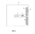
図1は、2つの1/4波長導電性セグメント(第1の長さ)20、30から形成される半波長ダイポールアンテナを示す。各1/4波長導電性セグメント20、30は、無線モジュール4に接続され、この無線モジュール4は、ベースバンドモジュール2に通信可能に接続されている。各導電性セグメントは、はんだボール又は他の相互接続素子40、あるいは集積回路パッケージ10の下に位置する他の導電性素子から形成されてもよい。アンテナが配置される、集積回路パッケージ及び回路基板の領域は、無線周波数エネルギーの送受信を妨害(干渉)し得る導電性素子を減らし、あるいは削減するように構成されてもよい。また、フリースペース内のアンテナの配置を最大限に活用するために、回路基板の端部又は端部近くにアンテナ構造20、30を位置することが望ましい。はんだボール40を、隣接のはんだボールに接触するように配置してもよく、導電性ペースト又ははんだを介して導電的に相互に結合してもよい。連続的な導電長を形成するために、熱の適用を通して、はんだボール40を溶解してもよい。また、回路基板及び/又は集積回路パッケージ内に形成された導電性トレースを通して、はんだボール40を互いに電気的に接続されてもよい。2つの導電性セグメント20、30は、端と端をつなぐ以外の方法で適応してもよい。相互接続素子、ICチップ、及び/又は回路基板のレイアウトにおけるスペース考慮のために、セグメント20、30は、例えば、90°、135°、45°などの角度をなして適応されてもよい。
FIG. 1 shows a half-wave dipole antenna formed from two quarter-wave conductive segments (first lengths) 20, 30. Each quarter-
図2は、集積回路パッケージ下のはんだボール40、50から形成される折り返しダイポールアンテナを示す。2つのはんだボール50は、アンテナ用のフィードポイント(供給ポイント)として用いられてもよい。
FIG. 2 shows a folded dipole antenna formed from
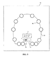
図3は、集積回路パッケージとともに、及び/又は集積回路パッケーが設置された回路基板上若しくはその中に配置され、はんだボール40及び導電性トレース60上に形成されたループアンテナを示す。導電性トレースから形成されているようにフィードポイント70を示している。本発明は、一つのループアンテナに限定されず、2つの(ダブル)ループアンテナ、3つの(トリプル)ループアンテナ、あるいは、1と3/4ループアンテナなどの分数ループアンテナを含む他のタイプのループアンテナで実行されてもよい。
FIG. 3 shows the loop antenna formed with the integrated circuit package and / or on or in the circuit board on which the integrated circuit package is installed and formed on the
図4〜図6Aは、集積回路パッケージ境界10外に広範囲に形成されるダブルアンテナを示す。図4は、2つの螺旋(スパイラル)90、100から形成され、回路基板トレース、入/出力ピンやはんだボールなどの相互接続素子、及び集積回路パッケージトレースの組み合わせから形成され得るトレース80を通して集積回路パッケージ10に結合されるダブルスパイラルアンテナを示す。図5及び図6は、ダブル方形波アンテナを示す。図5は、他のアンテナに近接するますます短い長さを形成するアンテナの内部端を示す。他の変形には、一定の長さと、他のアンテナに近接するますます長い長さとが含まれる。アンテナ形状は、直進する部分と、曲線部分とを交互に含んでもよい。図4及び図5のアンテナの類似部分と同様に、図6のアンテナにおいて、部分140が回路基板トレース又は外部導電性アタッチメントから形成されるのに対し、部分130は、相互接続素子、ICトレース、若しくは回路基板トレース、又はこれらの組み合わせから形成されてもよい。外部導電性アタッチメントは、表面設置のアンテナチップであってもよく、あるいは、粘着性側面若しくは機械的に取付可能な部分を有するキャリア材料によって曲げやすく結合され、十分に絶縁された導電素子であってもよい。機械的に取付可能な部分は、はんだ結合を介して取り付けられてもよい。あるいは、機械的に取付可能な部分は、ネジによって取り付けられてもよい。一つのアンテナは、曲線スパイラルであってもよく、他方のアンテナは、方形スパイラルであってもよい。これらの図面は、本発明の実例となる。アンテナパターンの他の変形は、本発明の精神及び範囲内にある。図6Aは、螺旋状アームを有するスター形状アンテナを示す。このアームは、2つ、3つ、4つ、5つ、あるいはそれ以上であってもよい。複数のアームは、それぞれ、鋭いZ形状、より緩やかなS形状を有していてもよく、あるいは、直線のセグメントでもよい。
4-6A show a double antenna formed extensively outside the integrated
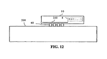
図7〜図12は、相互接続素子40を介して回路基板200上に設置された集積回路パッケージ10の断面図を示す。相互接続手段は、入/出力ピン、はんだボール、あるいは、回路基板200と集積回路10の間で電気信号を搬送する働きをする他の導電材料であってもよい。相互接続素子40は、ICチップパッケージ内のどの回路とも接続していない、ダミーの入/出力ピン、又はダミーのはんだパッドを含んでもよい。図示していないが、相互接続素子は、はんだや電気的導電性ペーストなどにより、選択的に溶解され、あるいは、接合されることによってパターンを形成するために、互いに電気的に結合されてもよい。図7は、互いに溶解され、あるいは、十分に長い連続した導電性パスを形成するためにそれらに適用される導電性接着剤を有する相互接続素子40上に形成されるアンテナを示す。この導電性パスは、送受信の望ましい中心周波数のためのアンテナとしての機能を果たす。図8は、相互接続素子40から形成されるアンテナを示す。この相互接続素子40は、アンテナに取り付けられた集積回路10の境界線を超えて延伸している。図9は、相互接続素子(第1の長さ)40と、回路基板200内に形成される導電性トレース(第2の長さ)250とから形成されるアンテナを示す。図10は、絶縁材料320によって接合される可撓性導電材料(例えば、リール上のテープ)から形成されるアンテナ310を示す。このアンテナは、特別に用意された導電性取付(接着)ポイント300を介して、集積回路10の上部に取り付けられてもよい。取付可能なアンテナは、取付ポイント300に結合する固定した回路基板上に形成されてもよい。その代わりに、導電性取付ポイント300は、回路基板200上に形成されてもよい。また、このアンテナは、回路基板200の延伸する平面に垂直あるいはわずかに垂直な指向性を許容するように、曲げることができる十分に堅い基板上に形成されてもよい。相互接続素子40は、このアンテナの一部を形成するために用いられてもよく、また、用いられなくてもよい。図11は、アンテナを形成するために用いられる、集積回路パッケージ10の導電性トレース(第3又は第2の長さ)350と、相互接続素子40と、導電性トレース(第2又は第3の長さ)250とを示す。図12は、アンテナを形成する、集積回路パッケージ10の導電性トレース350と、相互接続素子40とのみを示す。回路基板又はICパッケージ上に設置されたアンテナは、製造コストを削減し得る。
7 to 12 show cross-sectional views of the
図13A及び図13Bは、集積回路パッケージ10又は回路基板の端部に位置するピボッド可能なアンテナ450を示す。導電性トレースが、アンテナの一部を形成する。図示のように、車軸関節(pivot joint)400は、集積回路パッケージが設置された回路基板に水平な方向に移動することを可能にする。代わりの実施形態では、アンテナ450は、回路基板に対して垂直にピボッド(回転)してもよい。他のアンテナ素子は、相互接続素子を介して、集積回路パッケージ内に、及び/又は回路基板内にあってもよい。ピボッド可能な代わりに、アンテナは、格納式であってもよい。また、アンテナは、スナッピング動作(ポキッと折る動作)を有していてもよい。
13A and 13B show a
パッチ及びマイクロストリップアンテナは、本発明によって実行され得る。図14A及び図14Bは、パッチアンテナ500を示す。パッチアンテナは、低表面性状(形状)を提供し、種々の形状及び大きさに役に立ち得る。図14Aは、回路基板200内の2つの異なる平面に位置し、接地(グラウンド)平面550を挟み込むパッチアンテナ素子500及び510を示す。電気的相互接続520は、接地平面550の開口部を通して、2つの平面レベルのパッチアンテナを接続する。パッチアンテナ500は、集積回路パッケージ10の下に配置されてもよい。パッチアンテナは、回路基板200の領域内に配置されてもよい。この回路基板200は、最小数の他の導電性素子を有し、及び/又は、集積回路パッケージ、若しくは、RF信号送受信を最大限にするためにその上に設置された別々の素子を有しない。また、パッチアンテナは、回路基板、相互接続素子、又はICパッケージの1つの層を用いて具現化されてもよく、一つの素子であってもよい。図15は、スロット又は挿入されたパッチアンテナを示す。図16は、E又はF型マイクロストリップアンテナの変形例を示す。
Patches and microstrip antennas can be implemented with the present invention. 14A and 14B show a
図17A及び図17Bは、ヘリカルアンテナを示す。このヘリカルアンテナ素子は、集積回路パッケージ10か回路基板200のいずれかの中に完全に形成されてもよい。図17Aに示すように、ヘリカルアンテナは、3つの層、すなわち、集積回路パッケージ内の層800と、相互接続素子から形成される層と、回路基板内に形成される層830とを有する。図17Bに示すように、これらの層は、電気的導電性接続素子810、820を通して(あるいは、介して)、隣接する層と相互接続している。図17Bは、真ん中の層(相互接続素子から形成される層)が導電材料840によって層内にそれら自体相互接続される互接続素子40から形成されていることを示す。この導電材料は、導電性ペースト、はんだ、あるいは、回路基板及び/又は集積回路パッケージの表面に形成されるトレースであってもよい。その代わりに、ヘリカルアンテナは、ICチップパッケージ内、あるいは回路基板内に完全に形成されてもよい。
17A and 17B show a helical antenna. The helical antenna element may be completely formed in either the
機械的に埋め込まれたアンテナ、八木アンテナ、チップアンテナなどの他のアンテナを、本発明により実行してもよい。アンテナは、ユーザからRFエネルギーを変更するよう設計されてもよく、あるいは、送信信号の全指向性を提供するよう設計されてもよい。ICパッケージ上又はその近くに多数のアンテナを配置してもよく、これら多数のアンテナが、切換可能に選択され得る構成でもよい。 Other antennas such as mechanically embedded antennas, Yagi antennas, chip antennas may be implemented in accordance with the present invention. The antenna may be designed to change RF energy from the user, or may be designed to provide omnidirectionality of the transmitted signal. Multiple antennas may be arranged on or near the IC package, and the multiple antennas may be configured to be switchably selected.
図18は、相互接続素子40自体がアンテナを形成する実施形態を示す。図18は、送受信の質を向上するアンテナの分配を示す。相互接続素子は、はんだボール、入/出力ピン、拡張はんだボール、拡張入/出力ピン、あるいはその他の導電材料であってもよい。拡張相互接続素子は、実効アンテナ長を増加するために、ソケット又はその他の取付材料からピンを含んでもよい。
FIG. 18 shows an embodiment in which the
代わりの実施形態として、アンテナは、粘着性、プリント可能、パターン化可能、スプレー可能、あるいは溶解可能なはんだ及び/又は他の電気的導電材料から、全体的又は部分的に構成されてもよい。アンテナは、所定のパターン、すなわち、曲がりくねったもの、直線的長さ、分岐したものなどに形作られる、はんだ及び/又は他の電気的導電材料の長さから完全に構成されてもよい。この処理は、その材料を溶解し、あるいは、パターン化の絶縁塗料(防食剤)を用いることを必要としてもよい。導電性表面又は流動可能な材料を収集して接着する表面を有するくぼみは、堅くなる前に、溶解された導電材料を収集して保持するように、回路基板又は他の適当な表面中に配置され、あるいは、その上に選択的に分散されてもよい。溶解時のはんだ及びはんだボールは、表面張力効果を通して、集積回路パッケージ(例えば、BGA)上に、有益な自己センタリング効果をもたらし得る。その代わりに、アンテナは、マスクを通して、粘着性の電気的導電材料をスプレーすることによって形成されてもよい。はんだ及び/又は他の電気的導電材料の長さから形成されるならば、アンテナは、回路基板又はICチップパッケージ上に配置されてもよい。アンテナを形成するために、はんだのような流動性材料を適用することは、うまく制御されるのに必要である。なぜならば、アンテナを形成するためにあまりに多く、若しくはあまりに少なく、又は不規則に流動性材料を適用することは、その放射と、1つの製造されたアンテナから次のアンテナへのピックアップパターンとに影響を与え得るからである。処理の正確な制御は、他の素子と同様に、アンテナを製造するのに重要である。 As an alternative embodiment, the antenna may be constructed in whole or in part from adhesive and printable, patternable, sprayable, or meltable solder and / or other electrically conductive material. The antenna may consist entirely of a length of solder and / or other electrically conductive material that is shaped into a predetermined pattern, i.e., winding, linear length, branched, etc. This treatment may require dissolving the material or using a patterned insulating paint (anticorrosive). Indentations with conductive surfaces or surfaces that collect and adhere flowable material are placed on the circuit board or other suitable surface to collect and hold the dissolved conductive material before it hardens Or may be selectively distributed thereon. Melting solder and solder balls can provide a beneficial self-centering effect on integrated circuit packages (eg, BGA) through surface tension effects. Alternatively, the antenna may be formed by spraying an adhesive electrically conductive material through a mask. If formed from a length of solder and / or other electrically conductive material, the antenna may be placed on a circuit board or IC chip package. Applying a flowable material such as solder to form the antenna is necessary to be well controlled. This is because applying too much, too little, or irregularly flowable material to form an antenna will affect its radiation and pickup pattern from one manufactured antenna to the next. It is because it can give. Accurate control of the process is important for manufacturing the antenna as well as other elements.
アンテナを形成するために、種々の電気的導電材料を用いてもよい。アンテナは、少なくとも部分的に、銅、アルミニウム、ニッケル、蒼鉛、タングステン、銀、パラジウム、白金、亜鉛、クロム、モリブデン、鉛、アンチモン、スズ、若しくは金などの金属、あるいは、ポリシリコンなどの非金属導電材料から形成されてもよい。はんだ材料が用いられるならば、そのはんだ材料は、鉛、蒼鉛、スズ、アンチモン、銅、銀、亜鉛、及びインジウムからなるグループの2以上の材料を含んでもよく、スズ銀はんだ又はスズインジウムはんだなどの無鉛のものであってもよい。アンテナの異なる長さは、異なる材料から形成されてもよい。例えば、アンテナが集積回路内に部分的に形成され、相互接続素子を通して部分的に形成され、集積回路チップが取り付けられる回路基板内に部分的に形成される場合には、アンテナは、装置内のスペース利用を最大限にするために、ポリシリコン断面と、はんだ材料断面と、銅断面とを有してもよい。アンテナ性能を向上するために、材料特性マッチングを適用してもよい。 Various electrically conductive materials may be used to form the antenna. The antenna is at least partially a metal such as copper, aluminum, nickel, lead, tungsten, silver, palladium, platinum, zinc, chromium, molybdenum, lead, antimony, tin, or gold, or a non-metal such as polysilicon. It may be formed from a conductive material. If a solder material is used, the solder material may include two or more members of the group consisting of lead, lead, tin, antimony, copper, silver, zinc, and indium, such as tin silver solder or tin indium solder. It may be lead-free. Different lengths of the antenna may be formed from different materials. For example, if an antenna is partially formed in an integrated circuit, partially formed through interconnect elements, and partially formed in a circuit board to which the integrated circuit chip is attached, the antenna is To maximize space utilization, it may have a polysilicon cross section, a solder material cross section, and a copper cross section. Material property matching may be applied to improve antenna performance.
相互接続素子の周りに液状エポキシ樹脂などの誘電材料を配置し、あるいは、その誘電材料で満たしてもよい。アンテナ素子をより高い誘電率の材料(例えば、誘電体)で被覆することは、アンテナ素子のRFエネルギー捕獲を助けるので、この相互接続素子は、アンテナの全体長を減らすようにアンテナを形成している。アプリケータにより流動可能な形状で誘電材料を適用(塗布)し、その後、熱又は他の放射によりそれを固化してもよい。パターン化され、又はエッチングされる防食剤を通して、誘電材料を形成してもよい。ある誘電率の誘電材料を選択することを考慮すると、誘電率が高ければ高いほど、RFエネルギーは、アンテナ内に反射され、結果として生じるアンテナ性能をより狭い帯域にさせる。その代わりに、セラミックなどの誘電体基板上にアンテナを形成してもよい。 A dielectric material such as a liquid epoxy resin may be disposed around or filled with the interconnect element. Since coating the antenna element with a higher dielectric constant material (eg, a dielectric) helps capture the RF energy of the antenna element, the interconnect element forms the antenna to reduce the overall length of the antenna. Yes. The dielectric material may be applied (applied) in a flowable shape with an applicator and then solidified by heat or other radiation. The dielectric material may be formed through an anticorrosive that is patterned or etched. Considering the choice of a dielectric material with a certain dielectric constant, the higher the dielectric constant, the more RF energy is reflected into the antenna, causing the resulting antenna performance to be in a narrower band. Instead, an antenna may be formed on a dielectric substrate such as ceramic.
携帯電話器、パーソナルデータアシスタント(PDA)、パームトップ、ポケットパーソナルコンピュータ、プリンタ、スキャナ、デジタルカメラ、ゲームコンソール、MP3プレーヤー、無線ネットワークアクセスポイントなどの装置に、本発明のアンテナを用いてもよい。 The antenna of the present invention may be used in devices such as mobile phones, personal data assistants (PDAs), palmtops, pocket personal computers, printers, scanners, digital cameras, game consoles, MP3 players, and wireless network access points.
本発明及びそれに伴う多くの利点が、前述の記述により理解されると考えられる。また、本発明の範囲及び精神から逸脱することなく、あるいは、すべての物理的利点を犠牲にすることなく、構成要素(素子)の形状、構成及び配置における種々の変更がなされ得ることが明白であると考えられる。ここに前述の形状は、単にその実施形態を説明するために記述されただけであり、従って、添付の特許請求の範囲は、そのような変更を包含するように意図している。 The present invention and its many advantages will be understood by the foregoing description. It is also apparent that various changes in the shape, configuration and arrangement of components (elements) can be made without departing from the scope and spirit of the invention or without sacrificing all physical advantages. It is believed that there is. The foregoing shapes are now described merely to illustrate the embodiments, and the appended claims are therefore intended to cover such modifications.
本発明の多くの利点は、添付の図面を参照することにより、当業者により良く理解されるであろう。
Claims (6)
ボールグリッドアレイパッケージのチップに無線モジュールを搭載するステップと、
アンテナを作るのに適した前記ボールグリッドアレイパッケージ上にはんだボールの列を形成するステップと、
前記無線モジュールを前記はんだボールの列に接続するステップと、を含み、
前記無線モジュールが前記はんだボールの列を介して改良された送受信を可能にすることを特徴とする前記方法。A method of manufacturing a wireless module chip package, comprising:
Mounting a wireless module on a ball grid array package chip;
Forming an array of solder balls on the ball grid array package suitable for making an antenna;
Connecting the wireless module to the row of solder balls,
The method, wherein the wireless module enables improved transmission and reception through the solder ball array.
Applications Claiming Priority (2)
| Application Number | Priority Date | Filing Date | Title |
|---|---|---|---|
| US29172101P | 2001-05-17 | 2001-05-17 | |
| PCT/US2002/015402 WO2002093685A1 (en) | 2001-05-17 | 2002-05-17 | Ball grid array antenna |
Related Child Applications (1)
| Application Number | Title | Priority Date | Filing Date |
|---|---|---|---|
| JP2008053475A Division JP2008219897A (en) | 2001-05-17 | 2008-03-04 | Ball grid array antenna |
Publications (2)
| Publication Number | Publication Date |
|---|---|
| JP2004533166A JP2004533166A (en) | 2004-10-28 |
| JP4121860B2 true JP4121860B2 (en) | 2008-07-23 |
Family
ID=23121544
Family Applications (2)
| Application Number | Title | Priority Date | Filing Date |
|---|---|---|---|
| JP2002590451A Expired - Fee Related JP4121860B2 (en) | 2001-05-17 | 2002-05-17 | Ball grid array antenna |
| JP2008053475A Pending JP2008219897A (en) | 2001-05-17 | 2008-03-04 | Ball grid array antenna |
Family Applications After (1)
| Application Number | Title | Priority Date | Filing Date |
|---|---|---|---|
| JP2008053475A Pending JP2008219897A (en) | 2001-05-17 | 2008-03-04 | Ball grid array antenna |
Country Status (5)
| Country | Link |
|---|---|
| US (1) | US6914566B2 (en) |
| EP (1) | EP1413004A4 (en) |
| JP (2) | JP4121860B2 (en) |
| KR (1) | KR20040025680A (en) |
| WO (1) | WO2002093685A1 (en) |
Cited By (4)
| Publication number | Priority date | Publication date | Assignee | Title |
|---|---|---|---|---|
| US9160055B2 (en) | 2012-12-12 | 2015-10-13 | Kabushiki Kaisha Toshiba | Wireless device |
| US9178269B2 (en) | 2011-07-13 | 2015-11-03 | Kabushiki Kaisha Toshiba | Wireless apparatus |
| US9184492B2 (en) | 2010-09-24 | 2015-11-10 | Kabushiki Kaisha Toshiba | Radio device |
| US9543641B2 (en) | 2011-07-13 | 2017-01-10 | Kabushiki Kaisha Toshiba | Wireless apparatus |
Families Citing this family (62)
| Publication number | Priority date | Publication date | Assignee | Title |
|---|---|---|---|---|
| US6951596B2 (en) | 2002-01-18 | 2005-10-04 | Avery Dennison Corporation | RFID label technique |
| JP4121860B2 (en) * | 2001-05-17 | 2008-07-23 | サイプレス セミコンダクター コーポレーション | Ball grid array antenna |
| GB2383470B (en) * | 2001-11-12 | 2004-04-28 | Transense Technologies Plc | Self contained radio apparatus for transmission of data |
| CA2518611A1 (en) | 2002-04-24 | 2003-11-06 | Mineral Lassen Llc | Wireless communication device |
| US6982879B1 (en) * | 2003-07-19 | 2006-01-03 | Intel Corporation | Apparatus to provide connection between a microelectronic device and an antenna |
| US20050133901A1 (en) * | 2003-12-17 | 2005-06-23 | Texas Instruments Incorporated | System and method for delivering power to a semiconductor device |
| KR100584317B1 (en) * | 2004-02-06 | 2006-05-26 | 삼성전자주식회사 | Antenna apparatus for portable terminal |
| US20050203584A1 (en) * | 2004-03-10 | 2005-09-15 | Medtronic, Inc. | Telemetry antenna for an implantable medical device |
| US7317946B2 (en) * | 2004-03-10 | 2008-01-08 | Medtronic, Inc. | Telemetry antenna for an implantable medical device |
| US7202790B2 (en) * | 2004-08-13 | 2007-04-10 | Sensormatic Electronics Corporation | Techniques for tuning an antenna to different operating frequencies |
| US7292198B2 (en) | 2004-08-18 | 2007-11-06 | Ruckus Wireless, Inc. | System and method for an omnidirectional planar antenna apparatus with selectable elements |
| US7193562B2 (en) * | 2004-11-22 | 2007-03-20 | Ruckus Wireless, Inc. | Circuit board having a peripheral antenna apparatus with selectable antenna elements |
| US7500307B2 (en) | 2004-09-22 | 2009-03-10 | Avery Dennison Corporation | High-speed RFID circuit placement method |
| EP1797617A4 (en) | 2004-10-01 | 2009-08-12 | Rochemont L Pierre De | Ceramic antenna module and methods of manufacture thereof |
| KR100632807B1 (en) * | 2004-11-26 | 2006-10-16 | 삼성전자주식회사 | Semiconductor chip and TAB package comprising the same |
| US7358912B1 (en) | 2005-06-24 | 2008-04-15 | Ruckus Wireless, Inc. | Coverage antenna apparatus with selectable horizontal and vertical polarization elements |
| US7893882B2 (en) | 2007-01-08 | 2011-02-22 | Ruckus Wireless, Inc. | Pattern shaping of RF emission patterns |
| DE102005008063B4 (en) * | 2005-02-22 | 2008-05-15 | Fraunhofer-Gesellschaft zur Förderung der angewandten Forschung e.V. | antenna |
| US7607586B2 (en) * | 2005-03-28 | 2009-10-27 | R828 Llc | Semiconductor structure with RF element |
| US7623034B2 (en) | 2005-04-25 | 2009-11-24 | Avery Dennison Corporation | High-speed RFID circuit placement method and device |
| US7492325B1 (en) | 2005-10-03 | 2009-02-17 | Ball Aerospace & Technologies Corp. | Modular electronic architecture |
| US7555826B2 (en) | 2005-12-22 | 2009-07-07 | Avery Dennison Corporation | Method of manufacturing RFID devices |
| WO2007091554A1 (en) * | 2006-02-10 | 2007-08-16 | Matsushita Electric Industrial Co., Ltd. | Antenna device and electronic device using same |
| US7265719B1 (en) | 2006-05-11 | 2007-09-04 | Ball Aerospace & Technologies Corp. | Packaging technique for antenna systems |
| US20080122726A1 (en) * | 2006-11-27 | 2008-05-29 | Gil Levi | Low cost chip package with integrated RFantenna |
| JP4396785B2 (en) * | 2007-06-27 | 2010-01-13 | 株式会社村田製作所 | Wireless IC device |
| TW200933758A (en) * | 2008-01-17 | 2009-08-01 | En-Min Jow | Semiconductor package with antenna and manufacture method thereof |
| JP2009268691A (en) * | 2008-05-07 | 2009-11-19 | Olympus Medical Systems Corp | Antenna for capsule type medical device and capsule type medical device |
| WO2009156489A1 (en) | 2008-06-26 | 2009-12-30 | Thomson Licensing | Frontal block with integrated antenna |
| US7959598B2 (en) | 2008-08-20 | 2011-06-14 | Asante Solutions, Inc. | Infusion pump systems and methods |
| GB0815306D0 (en) * | 2008-08-21 | 2008-09-24 | Sarantel Ltd | An antenna and a method of manufacturing an antenna |
| FR2938982B1 (en) * | 2008-11-25 | 2012-01-13 | Thales Sa | NETWORK OF RADIANT ELEMENTS, AND ANTENNA COMPRISING SUCH A NETWORK. |
| US8466837B2 (en) * | 2008-12-31 | 2013-06-18 | Navcom Technology Inc. | Hooked turnstile antenna for navigation and communication |
| US8952858B2 (en) * | 2009-06-17 | 2015-02-10 | L. Pierre de Rochemont | Frequency-selective dipole antennas |
| US8922347B1 (en) | 2009-06-17 | 2014-12-30 | L. Pierre de Rochemont | R.F. energy collection circuit for wireless devices |
| CN102474535A (en) * | 2010-03-03 | 2012-05-23 | 古河电气工业株式会社 | Wireless transmission module and GSM multiband wireless transmission module |
| US8451618B2 (en) * | 2010-10-28 | 2013-05-28 | Infineon Technologies Ag | Integrated antennas in wafer level package |
| US9634403B2 (en) | 2012-02-14 | 2017-04-25 | Ruckus Wireless, Inc. | Radio frequency emission pattern shaping |
| US10186750B2 (en) | 2012-02-14 | 2019-01-22 | Arris Enterprises Llc | Radio frequency antenna array with spacing element |
| EP2667449A1 (en) * | 2012-05-23 | 2013-11-27 | Nxp B.V. | Integrated circuit package having an integrated antenna |
| TWI528468B (en) | 2012-05-30 | 2016-04-01 | 國立中山大學 | A mimo antenna, antenna unit thereof and a system in package having said antenna |
| US9490526B2 (en) * | 2012-08-14 | 2016-11-08 | Google Inc. | Wireless communication antennas in computer displays |
| KR101412946B1 (en) | 2012-12-20 | 2014-06-26 | 삼성전기주식회사 | Antenna and front end module |
| US9563834B2 (en) * | 2013-04-10 | 2017-02-07 | Honeywell International, Inc. | High temperature tolerant RFID tag |
| KR101466927B1 (en) * | 2013-06-03 | 2014-12-03 | (주)드림텍 | Mobile handset antenna mounting structure and method of mounting the same |
| CN105379007A (en) * | 2013-08-16 | 2016-03-02 | 英特尔公司 | Millimeter wave antenna structures with air-gap layer or cavity |
| KR102185196B1 (en) * | 2014-07-04 | 2020-12-01 | 삼성전자주식회사 | Apparatus for antenna in wireless communication device |
| EP3374905A1 (en) | 2016-01-13 | 2018-09-19 | Bigfoot Biomedical, Inc. | User interface for diabetes management system |
| CN112933333B (en) | 2016-01-14 | 2023-03-28 | 比格福特生物医药公司 | Adjusting insulin delivery rate |
| US9961774B2 (en) * | 2016-01-29 | 2018-05-01 | Peraso Technologies Inc. | Wireless communications assembly |
| US9660345B1 (en) | 2016-05-18 | 2017-05-23 | International Business Machines Corporation | Millimeter-wave communications on a multifunction platform |
| US9912061B2 (en) * | 2016-05-18 | 2018-03-06 | International Business Machines Corporation | Millimeter-wave communications on a multifunction platform |
| USD874471S1 (en) | 2017-06-08 | 2020-02-04 | Insulet Corporation | Display screen with a graphical user interface |
| US10153548B1 (en) * | 2017-08-03 | 2018-12-11 | Peraso Technologies Inc. | Wireless communications assembly with integrated active phased-array antenna |
| US10700410B2 (en) * | 2017-10-27 | 2020-06-30 | Mediatek Inc. | Antenna-in-package with better antenna performance |
| DE102018104662A1 (en) * | 2018-03-01 | 2019-09-05 | Endress+Hauser SE+Co. KG | Electronic circuit for generating, processing and / or processing high-frequency signals |
| USD928199S1 (en) | 2018-04-02 | 2021-08-17 | Bigfoot Biomedical, Inc. | Medication delivery device with icons |
| KR102526400B1 (en) * | 2018-09-06 | 2023-04-28 | 삼성전자주식회사 | An electronic device comprising a 5g antenna module |
| JP7306807B2 (en) | 2018-09-21 | 2023-07-11 | Necネットワーク・センサ株式会社 | Antennas and wireless communication systems |
| JP7129369B2 (en) * | 2019-03-26 | 2022-09-01 | シャープ株式会社 | Antenna device and communication terminal device |
| TW202145640A (en) * | 2020-05-28 | 2021-12-01 | 韋僑科技股份有限公司 | Radio frequency antenna module and method for making the same |
| USD977502S1 (en) | 2020-06-09 | 2023-02-07 | Insulet Corporation | Display screen with graphical user interface |
Family Cites Families (26)
| Publication number | Priority date | Publication date | Assignee | Title |
|---|---|---|---|---|
| GB2252452B (en) * | 1985-09-05 | 1992-12-16 | Plessey Co Plc | Improvements in or relating to hybrid structures |
| JP2621576B2 (en) * | 1990-05-16 | 1997-06-18 | 日本電気株式会社 | Monolithic microwave millimeter wave array antenna module |
| US5115245A (en) * | 1990-09-04 | 1992-05-19 | Hughes Aircraft Company | Single substrate microwave radar transceiver including flip-chip integrated circuits |
| US5621913A (en) * | 1992-05-15 | 1997-04-15 | Micron Technology, Inc. | System with chip to chip communication |
| JPH06140528A (en) * | 1992-10-22 | 1994-05-20 | Rohm Co Ltd | Microwave semiconductor device and manufacture thereof |
| JP3326935B2 (en) * | 1993-12-27 | 2002-09-24 | 株式会社日立製作所 | Small antenna for portable radio |
| GB2288286A (en) * | 1994-03-30 | 1995-10-11 | Plessey Semiconductors Ltd | Ball grid array arrangement |
| US5450090A (en) * | 1994-07-20 | 1995-09-12 | The Charles Stark Draper Laboratory, Inc. | Multilayer miniaturized microstrip antenna |
| JP3141692B2 (en) * | 1994-08-11 | 2001-03-05 | 松下電器産業株式会社 | Millimeter wave detector |
| JPH0969798A (en) * | 1995-09-01 | 1997-03-11 | Toshiba Corp | Portable radio machine and radio communication system using this machine |
| JP3303226B2 (en) * | 1996-02-09 | 2002-07-15 | 日本電信電話株式会社 | Flip chip mounting structure |
| US6805493B2 (en) * | 1996-03-12 | 2004-10-19 | 3M Innovative Properties Company | Optical connector assembly using partial large diameter alignment features |
| FI110394B (en) * | 1996-08-06 | 2003-01-15 | Filtronic Lk Oy | Combination antenna |
| EP0856376B1 (en) * | 1996-12-03 | 2000-02-09 | Lucent Technologies Inc. | Article comprising fine-grained solder compositions with dispersoid particles |
| JP3472430B2 (en) * | 1997-03-21 | 2003-12-02 | シャープ株式会社 | Antenna integrated high frequency circuit |
| US6046707A (en) * | 1997-07-02 | 2000-04-04 | Kyocera America, Inc. | Ceramic multilayer helical antenna for portable radio or microwave communication apparatus |
| JPH1167829A (en) * | 1997-08-22 | 1999-03-09 | Oki Electric Ind Co Ltd | Method for mounting electronic component, and electronic component and wiring board used in the method |
| US6201403B1 (en) * | 1997-09-22 | 2001-03-13 | Nortel Networks Limited | Integrated circuit package shielding characterization method and apparatus |
| US6018299A (en) * | 1998-06-09 | 2000-01-25 | Motorola, Inc. | Radio frequency identification tag having a printed antenna and method |
| JP2000278009A (en) * | 1999-03-24 | 2000-10-06 | Nec Corp | Microwave/millimeter wave circuit device |
| JP2000278037A (en) * | 1999-03-25 | 2000-10-06 | Tdk Corp | Chip antenna |
| JP2001077619A (en) * | 1999-09-01 | 2001-03-23 | Mitsubishi Electric Corp | Active antenna |
| US6297551B1 (en) * | 1999-09-22 | 2001-10-02 | Agere Systems Guardian Corp. | Integrated circuit packages with improved EMI characteristics |
| JP2001211019A (en) * | 2000-01-25 | 2001-08-03 | Hideo Suyama | Antenna equipment in transmission-reception modules and its producing method |
| US6563464B2 (en) * | 2001-03-19 | 2003-05-13 | International Business Machines Corporation | Integrated on-chip half-wave dipole antenna structure |
| JP4121860B2 (en) * | 2001-05-17 | 2008-07-23 | サイプレス セミコンダクター コーポレーション | Ball grid array antenna |
-
2002
- 2002-05-17 JP JP2002590451A patent/JP4121860B2/en not_active Expired - Fee Related
- 2002-05-17 EP EP02731804A patent/EP1413004A4/en not_active Withdrawn
- 2002-05-17 US US10/147,827 patent/US6914566B2/en not_active Expired - Lifetime
- 2002-05-17 WO PCT/US2002/015402 patent/WO2002093685A1/en active Application Filing
- 2002-05-17 KR KR10-2003-7014992A patent/KR20040025680A/en not_active Application Discontinuation
-
2008
- 2008-03-04 JP JP2008053475A patent/JP2008219897A/en active Pending
Cited By (4)
| Publication number | Priority date | Publication date | Assignee | Title |
|---|---|---|---|---|
| US9184492B2 (en) | 2010-09-24 | 2015-11-10 | Kabushiki Kaisha Toshiba | Radio device |
| US9178269B2 (en) | 2011-07-13 | 2015-11-03 | Kabushiki Kaisha Toshiba | Wireless apparatus |
| US9543641B2 (en) | 2011-07-13 | 2017-01-10 | Kabushiki Kaisha Toshiba | Wireless apparatus |
| US9160055B2 (en) | 2012-12-12 | 2015-10-13 | Kabushiki Kaisha Toshiba | Wireless device |
Also Published As
| Publication number | Publication date |
|---|---|
| US6914566B2 (en) | 2005-07-05 |
| EP1413004A4 (en) | 2004-07-21 |
| EP1413004A1 (en) | 2004-04-28 |
| WO2002093685A1 (en) | 2002-11-21 |
| JP2008219897A (en) | 2008-09-18 |
| US20020171591A1 (en) | 2002-11-21 |
| KR20040025680A (en) | 2004-03-24 |
| JP2004533166A (en) | 2004-10-28 |
Similar Documents
| Publication | Publication Date | Title |
|---|---|---|
| JP4121860B2 (en) | Ball grid array antenna | |
| US7924226B2 (en) | Tunable antenna | |
| US8525742B2 (en) | Compact multi-element antenna with phase shift | |
| US8531337B2 (en) | Antenna diversity system and slot antenna component | |
| US8791862B1 (en) | Semiconductor package having integrated antenna pad | |
| KR100638726B1 (en) | Antenna module and electric apparatus using the same | |
| CA2637038C (en) | Apparatus and methods for packaging integrated cirguit chips with antennas formed from package lead wires | |
| JP3990699B2 (en) | ANTENNA MODULE AND ELECTRONIC DEVICE HAVING THE SAME | |
| JP2005176366A (en) | Device and method which constitute antenna by using via formed as radiating element in substrate | |
| US20020135523A1 (en) | Loop antenna radiation and reference loops | |
| CN112397889A (en) | Chip antenna | |
| CN112086723A (en) | Antenna module and electronic device comprising same | |
| JP2003332825A (en) | Antenna module | |
| JP3253255B2 (en) | Antenna for portable wireless device and portable wireless device using the same | |
| JP2006005441A (en) | Thin-plate wideband antenna and information terminal device | |
| JP2001196824A (en) | Antenna device for transmission/reception module | |
| JP2020521403A (en) | Antenna assembly | |
| JP2001196829A (en) | Antenna device for transmission/reception module | |
| JP2001203519A (en) | Antenna system for transmission reception module | |
| KR100362177B1 (en) | Zigzag-shape Microstrip Patch Antenna comprising two patches | |
| JP2004165770A (en) | Inverted f antenna device | |
| JP2005530389A (en) | Metallized multiband antenna | |
| JP2001196827A (en) | Antenna device for transmission/reception module | |
| WO2006018905A1 (en) | Antenna |
Legal Events
| Date | Code | Title | Description |
|---|---|---|---|
| A621 | Written request for application examination |
Free format text: JAPANESE INTERMEDIATE CODE: A621 Effective date: 20050509 |
|
| A977 | Report on retrieval |
Free format text: JAPANESE INTERMEDIATE CODE: A971007 Effective date: 20070118 |
|
| A131 | Notification of reasons for refusal |
Free format text: JAPANESE INTERMEDIATE CODE: A131 Effective date: 20070612 |
|
| A601 | Written request for extension of time |
Free format text: JAPANESE INTERMEDIATE CODE: A601 Effective date: 20070903 |
|
| A602 | Written permission of extension of time |
Free format text: JAPANESE INTERMEDIATE CODE: A602 Effective date: 20070910 |
|
| A521 | Written amendment |
Free format text: JAPANESE INTERMEDIATE CODE: A523 Effective date: 20071012 |
|
| A131 | Notification of reasons for refusal |
Free format text: JAPANESE INTERMEDIATE CODE: A131 Effective date: 20071106 |
|
| A601 | Written request for extension of time |
Free format text: JAPANESE INTERMEDIATE CODE: A601 Effective date: 20080201 |
|
| A602 | Written permission of extension of time |
Free format text: JAPANESE INTERMEDIATE CODE: A602 Effective date: 20080208 |
|
| A521 | Written amendment |
Free format text: JAPANESE INTERMEDIATE CODE: A523 Effective date: 20080304 |
|
| TRDD | Decision of grant or rejection written | ||
| A01 | Written decision to grant a patent or to grant a registration (utility model) |
Free format text: JAPANESE INTERMEDIATE CODE: A01 Effective date: 20080401 |
|
| A61 | First payment of annual fees (during grant procedure) |
Free format text: JAPANESE INTERMEDIATE CODE: A61 Effective date: 20080430 |
|
| FPAY | Renewal fee payment (event date is renewal date of database) |
Free format text: PAYMENT UNTIL: 20110509 Year of fee payment: 3 |
|
| R150 | Certificate of patent or registration of utility model |
Free format text: JAPANESE INTERMEDIATE CODE: R150 |
|
| FPAY | Renewal fee payment (event date is renewal date of database) |
Free format text: PAYMENT UNTIL: 20120509 Year of fee payment: 4 |
|
| LAPS | Cancellation because of no payment of annual fees |