JP4113143B2 - 薄膜圧電体素子、サスペンション、及びハードディスク装置 - Google Patents
薄膜圧電体素子、サスペンション、及びハードディスク装置 Download PDFInfo
- Publication number
- JP4113143B2 JP4113143B2 JP2004072989A JP2004072989A JP4113143B2 JP 4113143 B2 JP4113143 B2 JP 4113143B2 JP 2004072989 A JP2004072989 A JP 2004072989A JP 2004072989 A JP2004072989 A JP 2004072989A JP 4113143 B2 JP4113143 B2 JP 4113143B2
- Authority
- JP
- Japan
- Prior art keywords
- film
- electrode
- region
- thin film
- resin film
- Prior art date
- Legal status (The legal status is an assumption and is not a legal conclusion. Google has not performed a legal analysis and makes no representation as to the accuracy of the status listed.)
- Expired - Lifetime
Links
- 239000010409 thin film Substances 0.000 title claims description 108
- 239000000725 suspension Substances 0.000 title claims description 32
- 239000010408 film Substances 0.000 claims description 168
- 239000011347 resin Substances 0.000 claims description 85
- 229920005989 resin Polymers 0.000 claims description 85
- 238000010586 diagram Methods 0.000 description 21
- 230000005540 biological transmission Effects 0.000 description 16
- 239000000758 substrate Substances 0.000 description 13
- 238000000034 method Methods 0.000 description 12
- 229910052751 metal Inorganic materials 0.000 description 9
- 239000002184 metal Substances 0.000 description 9
- 238000004519 manufacturing process Methods 0.000 description 7
- 239000000463 material Substances 0.000 description 7
- CPLXHLVBOLITMK-UHFFFAOYSA-N Magnesium oxide Chemical compound [Mg]=O CPLXHLVBOLITMK-UHFFFAOYSA-N 0.000 description 6
- NBIIXXVUZAFLBC-UHFFFAOYSA-N Phosphoric acid Chemical compound OP(O)(O)=O NBIIXXVUZAFLBC-UHFFFAOYSA-N 0.000 description 6
- 239000000853 adhesive Substances 0.000 description 6
- 230000001070 adhesive effect Effects 0.000 description 6
- 238000005530 etching Methods 0.000 description 5
- 238000009413 insulation Methods 0.000 description 5
- 238000006073 displacement reaction Methods 0.000 description 4
- 230000004048 modification Effects 0.000 description 4
- 238000012986 modification Methods 0.000 description 4
- 229910000147 aluminium phosphate Inorganic materials 0.000 description 3
- 229910052451 lead zirconate titanate Inorganic materials 0.000 description 3
- 239000000395 magnesium oxide Substances 0.000 description 3
- 239000007864 aqueous solution Substances 0.000 description 2
- 239000013078 crystal Substances 0.000 description 2
- 229920001721 polyimide Polymers 0.000 description 2
- 239000009719 polyimide resin Substances 0.000 description 2
- 229910001220 stainless steel Inorganic materials 0.000 description 2
- 239000010935 stainless steel Substances 0.000 description 2
- 238000003466 welding Methods 0.000 description 2
- 229910002113 barium titanate Inorganic materials 0.000 description 1
- JRPBQTZRNDNNOP-UHFFFAOYSA-N barium titanate Chemical compound [Ba+2].[Ba+2].[O-][Ti]([O-])([O-])[O-] JRPBQTZRNDNNOP-UHFFFAOYSA-N 0.000 description 1
- 238000005229 chemical vapour deposition Methods 0.000 description 1
- 239000004020 conductor Substances 0.000 description 1
- 230000008602 contraction Effects 0.000 description 1
- 230000007797 corrosion Effects 0.000 description 1
- 238000005260 corrosion Methods 0.000 description 1
- 230000006866 deterioration Effects 0.000 description 1
- PCHJSUWPFVWCPO-UHFFFAOYSA-N gold Chemical compound [Au] PCHJSUWPFVWCPO-UHFFFAOYSA-N 0.000 description 1
- 239000010931 gold Substances 0.000 description 1
- 229910052737 gold Inorganic materials 0.000 description 1
- 238000009434 installation Methods 0.000 description 1
- 229910052741 iridium Inorganic materials 0.000 description 1
- 238000000608 laser ablation Methods 0.000 description 1
- HFGPZNIAWCZYJU-UHFFFAOYSA-N lead zirconate titanate Chemical compound [O-2].[O-2].[O-2].[O-2].[O-2].[Ti+4].[Zr+4].[Pb+2] HFGPZNIAWCZYJU-UHFFFAOYSA-N 0.000 description 1
- 238000007747 plating Methods 0.000 description 1
- 229910052697 platinum Inorganic materials 0.000 description 1
- 238000004544 sputter deposition Methods 0.000 description 1
- 238000007740 vapor deposition Methods 0.000 description 1
Images


Classifications
-
- G—PHYSICS
- G11—INFORMATION STORAGE
- G11B—INFORMATION STORAGE BASED ON RELATIVE MOVEMENT BETWEEN RECORD CARRIER AND TRANSDUCER
- G11B5/00—Recording by magnetisation or demagnetisation of a record carrier; Reproducing by magnetic means; Record carriers therefor
- G11B5/48—Disposition or mounting of heads or head supports relative to record carriers ; arrangements of heads, e.g. for scanning the record carrier to increase the relative speed
- G11B5/4806—Disposition or mounting of heads or head supports relative to record carriers ; arrangements of heads, e.g. for scanning the record carrier to increase the relative speed specially adapted for disk drive assemblies, e.g. assembly prior to operation, hard or flexible disk drives
- G11B5/484—Integrated arm assemblies, e.g. formed by material deposition or by etching from single piece of metal or by lamination of materials forming a single arm/suspension/head unit
-
- G—PHYSICS
- G11—INFORMATION STORAGE
- G11B—INFORMATION STORAGE BASED ON RELATIVE MOVEMENT BETWEEN RECORD CARRIER AND TRANSDUCER
- G11B5/00—Recording by magnetisation or demagnetisation of a record carrier; Reproducing by magnetic means; Record carriers therefor
- G11B5/48—Disposition or mounting of heads or head supports relative to record carriers ; arrangements of heads, e.g. for scanning the record carrier to increase the relative speed
- G11B5/4806—Disposition or mounting of heads or head supports relative to record carriers ; arrangements of heads, e.g. for scanning the record carrier to increase the relative speed specially adapted for disk drive assemblies, e.g. assembly prior to operation, hard or flexible disk drives
- G11B5/486—Disposition or mounting of heads or head supports relative to record carriers ; arrangements of heads, e.g. for scanning the record carrier to increase the relative speed specially adapted for disk drive assemblies, e.g. assembly prior to operation, hard or flexible disk drives with provision for mounting or arranging electrical conducting means or circuits on or along the arm assembly
-
- H—ELECTRICITY
- H10—SEMICONDUCTOR DEVICES; ELECTRIC SOLID-STATE DEVICES NOT OTHERWISE PROVIDED FOR
- H10N—ELECTRIC SOLID-STATE DEVICES NOT OTHERWISE PROVIDED FOR
- H10N30/00—Piezoelectric or electrostrictive devices
- H10N30/20—Piezoelectric or electrostrictive devices with electrical input and mechanical output, e.g. functioning as actuators or vibrators
- H10N30/206—Piezoelectric or electrostrictive devices with electrical input and mechanical output, e.g. functioning as actuators or vibrators using only longitudinal or thickness displacement, e.g. d33 or d31 type devices
Description
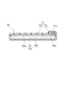
まず、基板Sを用意する。そして、この基板Sの上に、第2の電極膜75bを構成する材料からなる薄膜F1、薄膜圧電体73を構成する材料からなる薄膜F2、及び第1の電極膜75aを構成する材料からなる薄膜F3の順に積層して積層体L1を形成する(図9(a)及び(b)参照)。基板Sには、例えば酸化マグネシア(MgO)を材料とする単結晶基板等を用いることができる。薄膜F1,F3(第1及び第2の電極膜75a,75b)には、例えばPtやIr等の金属の他、導電性酸化物(例えば、IrO等)や導電性樹脂といった導電性材料を用いることができる。薄膜F2には、例えばチタン酸ジルコン酸鉛(PZT)、チタン酸バリウム等の圧電材料を用いることができる。薄膜F1〜F3を形成する方法には、例えばスパッタリング法、CVD法、レーザーアブレーション法等の方法を用いることができる。
次に、積層体L1を所望の形状に加工(パターニング)する(図10(a)及び(b)参照)。この工程(2)では、まず、積層体L1上に、第1領域70a、第2領域70c、及び第2の電極膜75bにおける第1領域70aとの第2領域70bとの間に位置する部分に対応する位置にレジスト膜(図示せず)を形成し、当該レジスト膜をマスク層として薄膜F1〜F3をエッチングにより除去する。続いて、上記レジスト膜を除去する。
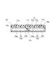
次に、第2の電極膜75b、薄膜圧電体73及び第1の電極膜75aの腐食を回避するために、基板S上において、第1領域70a、第2領域70b、及び第2の電極膜75bにおける第1領域70a及び第2領域70bとの間に位置する部分の表面を覆うように第1の樹脂膜77aを形成する(図11(a)及び(b)参照)。第1の樹脂膜77aは、当該第1の樹脂膜77aを構成する樹脂材料を塗布した後にベークすることにより形成される。
次に、第1の樹脂膜77a上であって、電極71a〜71cが形成される予定領域(薄膜圧電アクチュエータ70の根元領域)に第2の樹脂膜77bを形成する(図12(a)及び(b)参照)。第2の樹脂膜77bは、第1の樹脂膜77aと同じく、第2の樹脂膜77bを構成する樹脂材料を塗布した後にベークすることにより形成される。
次に、コンタクトホール78a〜78cに対応する位置に開口を有するレジスト膜(図示せず)を再度形成する。そして、このレジスト膜をマスク層として、コンタクトホール78a〜78cが形成されることにより露出した第1の電極膜75a及び第2の電極膜75b上に、蒸着とリフトオフ法とにより各電極71a〜71cを形成する(図13(a)及び(b)参照)。
Claims (9)
- 圧電体膜と、当該圧電体膜を挟むように配置される一対の電極膜とを含む積層体と、
前記積層体を覆うように形成される樹脂膜と、
前記樹脂膜上に形成され、前記電極膜に電気的に接続される電極と、を備え、
前記樹脂膜は、前記電極が形成される領域の厚みが前記積層体の変位する部分に対応する領域の厚みよりも厚くなるように形成されていることを特徴とする薄膜圧電体素子。 - 前記樹脂層は、前記積層体を覆うように形成される第1の樹脂膜と、前記電極が形成される前記領域に形成される第2の樹脂膜とを含んでいることを特徴とする請求項1に記載の薄膜圧電体素子。
- 前記積層体の上に接着される新たな積層体を更に備え、
前記新たな積層体は、圧電体膜と、当該圧電体膜を挟むように配置される一対の電極膜とを含むことを特徴とする請求項1に記載の薄膜圧電体素子。 - 薄膜磁気ヘッドを有するヘッドスライダが搭載されるサスペンションであって、
前記ヘッドスライダを当該サスペンションに対して相対的に変位させる薄膜圧電体素子を備え、
前記薄膜圧電体素子は、
圧電体膜と、当該圧電体膜を挟むように配置される一対の電極膜とを含む積層体と、
前記積層体を覆うように形成される樹脂膜と、
前記樹脂膜上に形成され、前記電極膜に電気的に接続される電極と、を有し、
前記樹脂膜は、前記電極が形成される領域の厚みが前記積層体の変位する部分に対応する領域の厚みよりも厚くなるように形成されていることを特徴とするサスペンション。 - 前記樹脂層は、前記積層体を覆うように形成される第1の樹脂膜と、前記電極が形成される前記領域に形成される第2の樹脂膜とを含んでいることを特徴とする請求項4に記載のサスペンション。
- 前記積層体の上に接着される新たな積層体を更に備え、
前記新たな積層体は、圧電体膜と、当該圧電体膜を挟むように配置される一対の電極膜とを含むことを特徴とする請求項4に記載のサスペンション。 - 記録媒体と、この記録媒体に対して記録又は再生の少なくとも一方を行う薄膜磁気ヘッドを有するヘッドスライダと、このヘッドスライダが搭載されるサスペンションとを備え、
前記サスペンションは、前記ヘッドスライダを当該サスペンションに対して相対的に変位させる薄膜圧電体素子を有し、
前記薄膜圧電体素子は、
圧電体膜と、当該圧電体膜を挟むように配置される一対の電極膜とを含む積層体と、
前記積層体を覆うように形成される樹脂膜と、
前記樹脂膜上に形成され、前記電極膜に電気的に接続される電極と、を有し、
前記樹脂膜は、前記電極が形成される領域の厚みが前記積層体の変位する部分に対応する領域の厚みよりも厚くなるように形成されていることを特徴とするハードディスク装置。 - 前記樹脂層は、前記積層体を覆うように形成される第1の樹脂膜と、前記電極が形成される前記領域に形成される第2の樹脂膜とを含んでいることを特徴とする請求項7に記載のハードディスク装置。
- 前記積層体の上に接着される新たな積層体を更に備え、
前記新たな積層体は、圧電体膜と、当該圧電体膜を挟むように配置される一対の電極膜とを含むことを特徴とする請求項7に記載のハードディスク装置。
Priority Applications (2)
| Application Number | Priority Date | Filing Date | Title |
|---|---|---|---|
| JP2004072989A JP4113143B2 (ja) | 2004-03-15 | 2004-03-15 | 薄膜圧電体素子、サスペンション、及びハードディスク装置 |
| US11/054,427 US7183696B2 (en) | 2004-03-15 | 2005-02-10 | Thin film piezoelectric element, suspension assembly, and hard disk drive |
Applications Claiming Priority (1)
| Application Number | Priority Date | Filing Date | Title |
|---|---|---|---|
| JP2004072989A JP4113143B2 (ja) | 2004-03-15 | 2004-03-15 | 薄膜圧電体素子、サスペンション、及びハードディスク装置 |
Publications (2)
| Publication Number | Publication Date |
|---|---|
| JP2005260161A JP2005260161A (ja) | 2005-09-22 |
| JP4113143B2 true JP4113143B2 (ja) | 2008-07-09 |
Family
ID=34918641
Family Applications (1)
| Application Number | Title | Priority Date | Filing Date |
|---|---|---|---|
| JP2004072989A Expired - Lifetime JP4113143B2 (ja) | 2004-03-15 | 2004-03-15 | 薄膜圧電体素子、サスペンション、及びハードディスク装置 |
Country Status (2)
| Country | Link |
|---|---|
| US (1) | US7183696B2 (ja) |
| JP (1) | JP4113143B2 (ja) |
Cited By (3)
| Publication number | Priority date | Publication date | Assignee | Title |
|---|---|---|---|---|
| US8038515B2 (en) | 2004-07-23 | 2011-10-18 | Oy Halton Group Ltd. | Control of exhaust systems |
| US10082299B2 (en) | 2008-12-03 | 2018-09-25 | Oy Halton Group Ltd. | Exhaust flow control system and method |
| JP7333435B1 (ja) | 2022-02-18 | 2023-08-24 | 本田技研工業株式会社 | 注湯装置及びその製造方法 |
Families Citing this family (9)
| Publication number | Priority date | Publication date | Assignee | Title |
|---|---|---|---|---|
| CN1828727A (zh) * | 2005-02-28 | 2006-09-06 | 新科实业有限公司 | 微驱动器及其磁头折片组合和磁盘驱动单元 |
| JP5032949B2 (ja) * | 2007-11-14 | 2012-09-26 | エイチジーエスティーネザーランドビーブイ | マイクロアクチュエータ、ヘッド・ジンバル・アセンブリ及びディスク・ドライブ装置 |
| US8677607B2 (en) | 2008-03-07 | 2014-03-25 | Tdk Corporation | Method of manufacturing magnetoresistive element |
| JP5943590B2 (ja) * | 2011-01-07 | 2016-07-05 | 日本発條株式会社 | 圧電素子の製造方法、圧電素子、圧電アクチュエータ、及びヘッド・サスペンション |
| JP5592289B2 (ja) * | 2011-02-25 | 2014-09-17 | Tdk株式会社 | 圧電素子及びその製造方法並びにその圧電素子を搭載したヘッドジンバルアセンブリ |
| US9875759B1 (en) | 2015-09-10 | 2018-01-23 | Magnecomp Corporation | Dual stage actuated suspension having shear-mode PZT actuators for rotating gimbal tongue |
| CN112520685B (zh) * | 2020-12-04 | 2024-03-01 | 青岛大学 | 一种双层薄膜致动器及其制备方法 |
| US20220415347A1 (en) * | 2021-06-29 | 2022-12-29 | Seagate Technology Llc | Low force actuator with a coupler piece and constrained layer construction |
| JP2023128424A (ja) * | 2022-03-03 | 2023-09-14 | 日本発條株式会社 | ディスク装置用サスペンション |
Family Cites Families (11)
| Publication number | Priority date | Publication date | Assignee | Title |
|---|---|---|---|---|
| US2266768A (en) * | 1941-03-08 | 1941-12-23 | Brush Dev Co | Means and method for protecting piezoelectric units |
| MY128744A (en) * | 2000-02-01 | 2007-02-28 | Matsushita Electric Ind Co Ltd | Head support machanism and thin film piezolectric actuator |
| JP3441429B2 (ja) | 2000-10-20 | 2003-09-02 | 松下電器産業株式会社 | 圧電体アクチュエータ、その製造方法、および圧電体アクチュエータの駆動方法 |
| US6617762B2 (en) * | 2000-08-03 | 2003-09-09 | Nec Tokin Ceramics Corporation | Microactuator device with a countermeasure for particles on a cut face thereof |
| JP4101492B2 (ja) | 2000-10-23 | 2008-06-18 | 松下電器産業株式会社 | ヘッド支持機構 |
| JP2002203998A (ja) * | 2000-12-28 | 2002-07-19 | Denso Corp | 圧電体素子及びその製造方法 |
| US6903491B2 (en) * | 2001-04-26 | 2005-06-07 | Matsushita Electric Industrial Co., Ltd. | Piezoelectric element, actuator, and inkjet head |
| JP2003061371A (ja) * | 2001-08-10 | 2003-02-28 | Fujitsu Ltd | 圧電アクチュエータ |
| SG103367A1 (en) * | 2001-11-02 | 2004-04-29 | Matsushita Electric Ind Co Ltd | Piezoelectric driving device |
| JP3846271B2 (ja) * | 2001-11-05 | 2006-11-15 | 松下電器産業株式会社 | 薄膜圧電体素子およびその製造方法 |
| JP4305016B2 (ja) * | 2002-03-18 | 2009-07-29 | セイコーエプソン株式会社 | 圧電アクチュエータユニット、及び、それを用いた液体噴射ヘッド |
-
2004
- 2004-03-15 JP JP2004072989A patent/JP4113143B2/ja not_active Expired - Lifetime
-
2005
- 2005-02-10 US US11/054,427 patent/US7183696B2/en active Active
Cited By (3)
| Publication number | Priority date | Publication date | Assignee | Title |
|---|---|---|---|---|
| US8038515B2 (en) | 2004-07-23 | 2011-10-18 | Oy Halton Group Ltd. | Control of exhaust systems |
| US10082299B2 (en) | 2008-12-03 | 2018-09-25 | Oy Halton Group Ltd. | Exhaust flow control system and method |
| JP7333435B1 (ja) | 2022-02-18 | 2023-08-24 | 本田技研工業株式会社 | 注湯装置及びその製造方法 |
Also Published As
| Publication number | Publication date |
|---|---|
| US7183696B2 (en) | 2007-02-27 |
| US20050200237A1 (en) | 2005-09-15 |
| JP2005260161A (ja) | 2005-09-22 |
Similar Documents
| Publication | Publication Date | Title |
|---|---|---|
| US7183696B2 (en) | Thin film piezoelectric element, suspension assembly, and hard disk drive | |
| US7420785B2 (en) | Suspension assembly, hard disk drive, and method of manufacturing suspension assembly | |
| JP7145771B2 (ja) | ハードディスクドライブサスペンション用多層マイクロアクチュエータ | |
| US8189301B2 (en) | Wireless microactuator motor assembly for use in a hard disk drive suspension, and mechanical and electrical connections thereto | |
| JP4897767B2 (ja) | 薄膜圧電体素子及びその製造方法並びにそれを用いたヘッドジンバルアセンブリ、及びそのヘッドジンバルアセンブリを用いたハードディスクドライブ | |
| US20090086379A1 (en) | Head suspension and piezoelectric actuator | |
| JP2006244690A (ja) | 回転可能な圧電マイクロアクチュエーター、及びヘッドジンバルアセンブリ、並びにディスクドライブユニット | |
| JP2006244691A (ja) | マイクロアクチュエータ、これを用いたヘッドジンバルアセンブリ及びディスクドライブ | |
| JP6054593B2 (ja) | 圧電素子の電気的接続構造 | |
| US11348609B2 (en) | Head suspension assembly and disk device | |
| US11694715B2 (en) | Head suspension assembly and disk device | |
| JP2001332041A (ja) | ディスク装置用薄膜圧電体アクチュエーターおよびその製造方法 | |
| JP2008034091A (ja) | マイクロアクチュエータ、これを備えたヘッドジンバルアセンブリ及びその製造方法 | |
| JP2007149327A (ja) | マイクロアクチュエータ、これを用いたヘッドジンバルアセンブリ及びディスクドライブ | |
| WO2000030081A1 (fr) | Mecanisme de support de tete d'enregistrement/lecture et appareil d'enregistrement/lecture | |
| JP2014106985A (ja) | ヘッドジンバルアセンブリの製造方法およびそれを構成するフレクシャの製造方法並びにヘッドジンバルアセンブリおよびフレクシャの製造に用いられるフレクシャシート | |
| US7518833B2 (en) | Micro-actuator with electric spark preventing structure, HGA, and disk drive unit with the same, and manufacturing method thereof | |
| JP6096637B2 (ja) | ヘッドジンバルアッセンブリおよびこれを備えたディスク装置 | |
| US20080273272A1 (en) | Micro-Actuator, HGA Equipped with the Micro-Actuator and Method for Manufacturing the HGA | |
| JP4071203B2 (ja) | 薄膜圧電体素子の接着方法 | |
| JP2007095275A (ja) | 電気的スパーク防止構造を備えたマイクロアクチュエータ、これを用いた磁気ヘッドアセンブリ及びディスク装置、マイクロアクチュエータの製造方法 | |
| JP4581447B2 (ja) | 薄膜圧電体素子の製造方法及びサスペンションの製造方法 | |
| JP4167191B2 (ja) | サスペンション、ヘッドジンバルアセンブリ、及びハードディスク装置 | |
| JP5303776B2 (ja) | サスペンション、ヘッドジンバルアセンブリ及びその製造方法及び磁気ディスクドライブユニット | |
| JP4197654B2 (ja) | ヘッドジンバルアセンブリ及びハードディスク装置 |
Legal Events
| Date | Code | Title | Description |
|---|---|---|---|
| A977 | Report on retrieval |
Free format text: JAPANESE INTERMEDIATE CODE: A971007 Effective date: 20060417 |
|
| TRDD | Decision of grant or rejection written | ||
| A01 | Written decision to grant a patent or to grant a registration (utility model) |
Free format text: JAPANESE INTERMEDIATE CODE: A01 Effective date: 20080408 |
|
| A61 | First payment of annual fees (during grant procedure) |
Free format text: JAPANESE INTERMEDIATE CODE: A61 Effective date: 20080410 |
|
| R150 | Certificate of patent or registration of utility model |
Ref document number: 4113143 Country of ref document: JP Free format text: JAPANESE INTERMEDIATE CODE: R150 Free format text: JAPANESE INTERMEDIATE CODE: R150 |
|
| FPAY | Renewal fee payment (event date is renewal date of database) |
Free format text: PAYMENT UNTIL: 20110418 Year of fee payment: 3 |
|
| FPAY | Renewal fee payment (event date is renewal date of database) |
Free format text: PAYMENT UNTIL: 20110418 Year of fee payment: 3 |
|
| FPAY | Renewal fee payment (event date is renewal date of database) |
Free format text: PAYMENT UNTIL: 20120418 Year of fee payment: 4 |
|
| FPAY | Renewal fee payment (event date is renewal date of database) |
Free format text: PAYMENT UNTIL: 20130418 Year of fee payment: 5 |
|
| FPAY | Renewal fee payment (event date is renewal date of database) |
Free format text: PAYMENT UNTIL: 20140418 Year of fee payment: 6 |