JP4113143B2 - Thin film piezoelectric element, suspension, and hard disk device - Google Patents
Thin film piezoelectric element, suspension, and hard disk device Download PDFInfo
- Publication number
- JP4113143B2 JP4113143B2 JP2004072989A JP2004072989A JP4113143B2 JP 4113143 B2 JP4113143 B2 JP 4113143B2 JP 2004072989 A JP2004072989 A JP 2004072989A JP 2004072989 A JP2004072989 A JP 2004072989A JP 4113143 B2 JP4113143 B2 JP 4113143B2
- Authority
- JP
- Japan
- Prior art keywords
- film
- electrode
- region
- thin film
- resin film
- Prior art date
- Legal status (The legal status is an assumption and is not a legal conclusion. Google has not performed a legal analysis and makes no representation as to the accuracy of the status listed.)
- Expired - Lifetime
Links
- 239000010409 thin film Substances 0.000 title claims description 108
- 239000000725 suspension Substances 0.000 title claims description 32
- 239000010408 film Substances 0.000 claims description 168
- 239000011347 resin Substances 0.000 claims description 85
- 229920005989 resin Polymers 0.000 claims description 85
- 238000010586 diagram Methods 0.000 description 21
- 230000005540 biological transmission Effects 0.000 description 16
- 239000000758 substrate Substances 0.000 description 13
- 238000000034 method Methods 0.000 description 12
- 229910052751 metal Inorganic materials 0.000 description 9
- 239000002184 metal Substances 0.000 description 9
- 238000004519 manufacturing process Methods 0.000 description 7
- 239000000463 material Substances 0.000 description 7
- CPLXHLVBOLITMK-UHFFFAOYSA-N Magnesium oxide Chemical compound [Mg]=O CPLXHLVBOLITMK-UHFFFAOYSA-N 0.000 description 6
- NBIIXXVUZAFLBC-UHFFFAOYSA-N Phosphoric acid Chemical compound OP(O)(O)=O NBIIXXVUZAFLBC-UHFFFAOYSA-N 0.000 description 6
- 239000000853 adhesive Substances 0.000 description 6
- 230000001070 adhesive effect Effects 0.000 description 6
- 238000005530 etching Methods 0.000 description 5
- 238000009413 insulation Methods 0.000 description 5
- 238000006073 displacement reaction Methods 0.000 description 4
- 230000004048 modification Effects 0.000 description 4
- 238000012986 modification Methods 0.000 description 4
- 229910000147 aluminium phosphate Inorganic materials 0.000 description 3
- 229910052451 lead zirconate titanate Inorganic materials 0.000 description 3
- 239000000395 magnesium oxide Substances 0.000 description 3
- 239000007864 aqueous solution Substances 0.000 description 2
- 239000013078 crystal Substances 0.000 description 2
- 229920001721 polyimide Polymers 0.000 description 2
- 239000009719 polyimide resin Substances 0.000 description 2
- 229910001220 stainless steel Inorganic materials 0.000 description 2
- 239000010935 stainless steel Substances 0.000 description 2
- 238000003466 welding Methods 0.000 description 2
- 229910002113 barium titanate Inorganic materials 0.000 description 1
- JRPBQTZRNDNNOP-UHFFFAOYSA-N barium titanate Chemical compound [Ba+2].[Ba+2].[O-][Ti]([O-])([O-])[O-] JRPBQTZRNDNNOP-UHFFFAOYSA-N 0.000 description 1
- 238000005229 chemical vapour deposition Methods 0.000 description 1
- 239000004020 conductor Substances 0.000 description 1
- 230000008602 contraction Effects 0.000 description 1
- 230000007797 corrosion Effects 0.000 description 1
- 238000005260 corrosion Methods 0.000 description 1
- 230000006866 deterioration Effects 0.000 description 1
- PCHJSUWPFVWCPO-UHFFFAOYSA-N gold Chemical compound [Au] PCHJSUWPFVWCPO-UHFFFAOYSA-N 0.000 description 1
- 239000010931 gold Substances 0.000 description 1
- 229910052737 gold Inorganic materials 0.000 description 1
- 238000009434 installation Methods 0.000 description 1
- 229910052741 iridium Inorganic materials 0.000 description 1
- 238000000608 laser ablation Methods 0.000 description 1
- HFGPZNIAWCZYJU-UHFFFAOYSA-N lead zirconate titanate Chemical compound [O-2].[O-2].[O-2].[O-2].[O-2].[Ti+4].[Zr+4].[Pb+2] HFGPZNIAWCZYJU-UHFFFAOYSA-N 0.000 description 1
- 238000007747 plating Methods 0.000 description 1
- 229910052697 platinum Inorganic materials 0.000 description 1
- 238000004544 sputter deposition Methods 0.000 description 1
- 238000007740 vapor deposition Methods 0.000 description 1
Images


Classifications
-
- G—PHYSICS
- G11—INFORMATION STORAGE
- G11B—INFORMATION STORAGE BASED ON RELATIVE MOVEMENT BETWEEN RECORD CARRIER AND TRANSDUCER
- G11B5/00—Recording by magnetisation or demagnetisation of a record carrier; Reproducing by magnetic means; Record carriers therefor
- G11B5/48—Disposition or mounting of heads or head supports relative to record carriers ; arrangements of heads, e.g. for scanning the record carrier to increase the relative speed
- G11B5/4806—Disposition or mounting of heads or head supports relative to record carriers ; arrangements of heads, e.g. for scanning the record carrier to increase the relative speed specially adapted for disk drive assemblies, e.g. assembly prior to operation, hard or flexible disk drives
- G11B5/484—Integrated arm assemblies, e.g. formed by material deposition or by etching from single piece of metal or by lamination of materials forming a single arm/suspension/head unit
-
- G—PHYSICS
- G11—INFORMATION STORAGE
- G11B—INFORMATION STORAGE BASED ON RELATIVE MOVEMENT BETWEEN RECORD CARRIER AND TRANSDUCER
- G11B5/00—Recording by magnetisation or demagnetisation of a record carrier; Reproducing by magnetic means; Record carriers therefor
- G11B5/48—Disposition or mounting of heads or head supports relative to record carriers ; arrangements of heads, e.g. for scanning the record carrier to increase the relative speed
- G11B5/4806—Disposition or mounting of heads or head supports relative to record carriers ; arrangements of heads, e.g. for scanning the record carrier to increase the relative speed specially adapted for disk drive assemblies, e.g. assembly prior to operation, hard or flexible disk drives
- G11B5/486—Disposition or mounting of heads or head supports relative to record carriers ; arrangements of heads, e.g. for scanning the record carrier to increase the relative speed specially adapted for disk drive assemblies, e.g. assembly prior to operation, hard or flexible disk drives with provision for mounting or arranging electrical conducting means or circuits on or along the arm assembly
-
- H—ELECTRICITY
- H10—SEMICONDUCTOR DEVICES; ELECTRIC SOLID-STATE DEVICES NOT OTHERWISE PROVIDED FOR
- H10N—ELECTRIC SOLID-STATE DEVICES NOT OTHERWISE PROVIDED FOR
- H10N30/00—Piezoelectric or electrostrictive devices
- H10N30/20—Piezoelectric or electrostrictive devices with electrical input and mechanical output, e.g. functioning as actuators or vibrators
- H10N30/206—Piezoelectric or electrostrictive devices with electrical input and mechanical output, e.g. functioning as actuators or vibrators using only longitudinal or thickness displacement, e.g. d33 or d31 type devices
Description
本発明は、薄膜圧電体素子、サスペンション、及びハードディスク装置に関する。 The present invention relates to a thin film piezoelectric element, a suspension, and a hard disk device.
ハードディスク等の記録媒体に磁気情報を記録及び再生する薄膜磁気ヘッドは、いわゆるヘッドスライダに形成されている。このヘッドスライダを、サスペンションの先端領域に搭載することにより、ヘッドジンバルアセンブリ(HGA)が構成される。一般的に、このサスペンションは、SUS等で形成されたロードビームに可撓性のフレクシャを重ねたものであり、フレクシャには薄膜磁気ヘッドの記録/再生用の配線が施されている。また、このようなサスペンションの基端側は、ボイスコイルモータ(VCM)で駆動されるアクチュエータアームに連結される。そして、サスペンションとアクチュエータアームを連結したものにVCMコイル等を取り付けることにより、所謂ヘッドスタックアセンブリ(HSA)が構成されている。 A thin film magnetic head for recording and reproducing magnetic information on a recording medium such as a hard disk is formed on a so-called head slider. A head gimbal assembly (HGA) is configured by mounting this head slider on the tip end region of the suspension. Generally, this suspension is obtained by superposing a flexible flexure on a load beam formed of SUS or the like, and a wiring for recording / reproducing of a thin film magnetic head is applied to the flexure. Further, the base end side of such a suspension is connected to an actuator arm driven by a voice coil motor (VCM). And what is called a head stack assembly (HSA) is comprised by attaching a VCM coil etc. to what connected the suspension and the actuator arm.
ところで、近年のハードディスクの高記録密度化、特にトラック幅の狭小化に伴い、ヘッドスライダを高精度で微小量駆動させる技術が求められている。そこで従来、下記特許文献1に示すように、上記サスペンションとアクチュエータアームとの連結部分に、圧電素子を利用した薄膜圧電体素子を配置するヘッドジンバルアセンブリが提案されていた。これは所謂2段変動式のアセンブリであり、第1段階として、薄膜磁気ヘッドの比較的大きな移動はボイスコイルモータによるアクチュエータアームの駆動で制御し、第2段階として、トラッキング補正等の微小な移動は薄膜圧電体素子によるサスペンションの駆動により制御しようとするものである。
By the way, with the recent increase in recording density of hard disks, in particular, the narrowing of the track width, a technique for driving a head slider with a minute amount with high accuracy is required. Therefore, conventionally, as shown in
ところが、このような2段変動式のヘッドジンバルアセンブリでは、薄膜圧電体素子によって長尺のサスペンション全体を駆動させる必要があるため、トラッキングの高精度化に限界があった。このため、例えば下記特許文献2に開示されているように、ヘッドスライダとサスペンションの間に薄膜圧電体素子を設ける装置が提案されている。この装置によれば、薄膜圧電体素子は長尺サスペンションそのものを駆動させる必要が無く、直接的にヘッドスライダを駆動させることができるため、より高精度のトラッキングを実現することができる。 However, in such a two-stage fluctuation type head gimbal assembly, it is necessary to drive the entire long suspension by the thin film piezoelectric element, so that there is a limit to the high accuracy of tracking. For this reason, as disclosed in, for example, Patent Document 2 below, an apparatus in which a thin film piezoelectric element is provided between a head slider and a suspension has been proposed. According to this apparatus, it is not necessary for the thin film piezoelectric element to drive the long suspension itself, and the head slider can be directly driven, so that higher-precision tracking can be realized.
特許文献2に開示された薄膜圧電体素子は、圧電体膜と、当該圧電体膜を挟むように配置される一対の電極膜とを含む積層体を備える。更に、この薄膜圧電体素子は、積層体を覆うように形成される樹脂膜と、当該樹脂膜上に形成され、電極膜に電気的に接続される電極とを備える。
しかしながら、上記従来の薄膜圧電体素子には、次のような問題があった。樹脂膜の厚みが厚いと、積層体(圧電体膜)の変位を阻害して圧電性が低下する懼れがあると共に、樹脂膜が硬化する際の応力により積層体が反ってしまう懼れがある。一方、樹脂膜の厚みが薄いと、電極膜と電極との間において絶縁不良が生じてしまう懼れがある。 However, the conventional thin film piezoelectric element has the following problems. If the resin film is thick, the displacement of the laminated body (piezoelectric film) may be hindered and the piezoelectricity may be lowered, and the laminated body may be warped by stress when the resin film is cured. is there. On the other hand, if the thickness of the resin film is thin, there is a possibility that an insulation failure occurs between the electrode film and the electrode.
本発明の目的は、圧電性を損なうことなく、電極膜と電極との間の絶縁不良の発生を抑制することが可能な薄膜圧電体素子、サスペンション、及びハードディスク装置を提供することにある。 An object of the present invention is to provide a thin film piezoelectric element, a suspension, and a hard disk device capable of suppressing the occurrence of insulation failure between an electrode film and an electrode without impairing the piezoelectricity.
本発明に係る薄膜圧電体素子は、圧電体膜と、当該圧電体膜を挟むように配置される一対の電極膜とを含む積層体と、積層体を覆うように形成される樹脂膜と、樹脂膜上に形成され、電極膜に電気的に接続される電極と、を備え、樹脂膜は、電極が形成される領域の厚みが積層体の変位する部分に対応する領域の厚みよりも厚くなるように形成されていることを特徴とする。 A thin film piezoelectric element according to the present invention includes a laminate including a piezoelectric film and a pair of electrode films arranged so as to sandwich the piezoelectric film, a resin film formed so as to cover the laminate, An electrode formed on the resin film and electrically connected to the electrode film, and the resin film is thicker than the region corresponding to the displaced portion of the laminate. It is formed so that it may become.
一方、本発明に係るサスペンションは、薄膜磁気ヘッドを有するヘッドスライダが搭載されるサスペンションであって、ヘッドスライダを当該サスペンションに対して相対的に変位させる薄膜圧電体素子を備え、薄膜圧電体素子は、圧電体膜と、当該圧電体膜を挟むように配置される一対の電極膜とを含む積層体と、積層体を覆うように形成される樹脂膜と、樹脂膜上に形成され、電極膜に電気的に接続される電極と、を有し、樹脂膜は、電極が形成される領域の厚みが積層体の変位する部分に対応する領域の厚みよりも厚くなるように形成されていることを特徴とする。 On the other hand, a suspension according to the present invention is a suspension on which a head slider having a thin film magnetic head is mounted, and includes a thin film piezoelectric element that displaces the head slider relative to the suspension. A laminated body including a piezoelectric film and a pair of electrode films arranged so as to sandwich the piezoelectric film, a resin film formed so as to cover the laminated body, and an electrode film formed on the resin film And the resin film is formed so that the thickness of the region where the electrode is formed is thicker than the thickness of the region corresponding to the displaced portion of the laminate. It is characterized by.
更に、本発明に係るハードディスク装置は、記録媒体と、この記録媒体に対して記録又は再生の少なくとも一方を行う薄膜磁気ヘッドを有するヘッドスライダと、このヘッドスライダが搭載されるサスペンションとを備え、サスペンションは、ヘッドスライダを当該サスペンションに対して相対的に変位させる薄膜圧電体素子を有し、薄膜圧電体素子は、圧電体膜と、当該圧電体膜を挟むように配置される一対の電極膜とを含む積層体と、積層体を覆うように形成される樹脂膜と、樹脂膜上に形成され、電極膜に電気的に接続される電極と、を有し、樹脂膜は、電極が形成される領域の厚みが積層体の変位する部分に対応する領域の厚みよりも厚くなるように形成されていることを特徴とする。 Furthermore, a hard disk device according to the present invention includes a recording medium, a head slider having a thin film magnetic head that performs at least one of recording and reproduction on the recording medium, and a suspension on which the head slider is mounted. Has a thin film piezoelectric element that displaces the head slider relative to the suspension, and the thin film piezoelectric element includes a piezoelectric film and a pair of electrode films arranged so as to sandwich the piezoelectric film. A laminate including: a resin film formed so as to cover the laminate; and an electrode formed on the resin film and electrically connected to the electrode film. The thickness of the region to be formed is formed so as to be thicker than the thickness of the region corresponding to the displaced portion of the laminate.
これら、本発明に係る薄膜圧電体素子、サスペンション、及びハードディスク装置それぞれによれば、樹脂膜における電極が形成される領域の厚みが積層体の変位する部分に対応する領域の厚みよりも厚いので、電極膜と電極との間隔が比較的大きくなり、電極膜と電極との間の絶縁不良の発生を抑制することができる。また、樹脂膜における積層体の変位する部分に対応する領域の厚みは、上記電極が形成される領域の厚みがより薄くなるので、積層体(圧電体膜)の変位が阻害されるようなことはなく、圧電性が低下するのを抑制できる。また、積層体が反ってしまうのも抑制できる。 According to each of these thin film piezoelectric elements, suspensions, and hard disk devices according to the present invention, the thickness of the region where the electrode is formed in the resin film is thicker than the thickness of the region corresponding to the displaced part of the laminate, The distance between the electrode film and the electrode becomes relatively large, and the occurrence of insulation failure between the electrode film and the electrode can be suppressed. In addition, the thickness of the region of the resin film corresponding to the displaced portion of the laminate is such that the thickness of the region where the electrode is formed becomes thinner, so that the displacement of the laminate (piezoelectric film) is hindered. There is no, and it can suppress that piezoelectricity falls. Moreover, it can also suppress that a laminated body warps.
また、上記樹脂層は、積層体を覆うように形成される第1の樹脂膜と、電極が形成される領域に形成される第2の樹脂膜とを含んでいることが好ましい。この場合、電極が形成される領域の厚みが積層体の変位する部分に対応する領域の厚みよりも厚くされた樹脂膜を極めて容易に形成することができる。 Moreover, it is preferable that the said resin layer contains the 1st resin film formed so that a laminated body may be covered, and the 2nd resin film formed in the area | region in which an electrode is formed. In this case, it is possible to very easily form a resin film in which the thickness of the region where the electrode is formed is larger than the thickness of the region corresponding to the displaced portion of the laminate.
本発明によれば、圧電性を損なうことなく、電極膜と電極との間の絶縁不良の発生を抑制することが可能な薄膜圧電体素子、サスペンション、及びハードディスク装置を提供することができる。 According to the present invention, it is possible to provide a thin film piezoelectric element, a suspension, and a hard disk device capable of suppressing the occurrence of insulation failure between an electrode film and an electrode without impairing the piezoelectricity.
以下、添付図面を参照して、本発明に係る薄膜圧電体素子、サスペンション、及びハードディスク装置の好適な実施形態について詳細に説明する。なお、説明において、同一要素又は同一機能を有する要素には、同一符号を用いることとし、重複する説明は省略する。 DESCRIPTION OF EMBODIMENTS Hereinafter, preferred embodiments of a thin film piezoelectric element, a suspension, and a hard disk device according to the present invention will be described in detail with reference to the accompanying drawings. In the description, the same reference numerals are used for the same elements or elements having the same function, and redundant description is omitted.
図1は、本実施形態のハードディスク装置を示す概略構成図である。ハードディスク装置1は、筐体5内に、記録媒体としてのハードディスク10と、これに磁気情報を記録及び再生するヘッドスタックアセンブリ(HSA)20とを備えている。ハードディスク10は、図示を省略するモータによって回転させられる。更に、ハードディスク装置1には、ハードディスク10への情報の記録及び再生等の各種制御を行う制御部15、及び、薄膜磁気ヘッドをハードディスク10の上から退避させておくためのランプ機構16が内蔵されている。
FIG. 1 is a schematic configuration diagram showing the hard disk device of the present embodiment. The
ヘッドスタックアセンブリ20は、ボイスコイルモータ(VCM)により支軸21周りに回転自在に支持されたアクチュエータアーム22と、このアクチュエータアーム22に接続されたヘッドジンバルアセンブリ(以下、「HGA」と称す)30とから構成される組立て体を、図の奥行き方向に複数個積層したものである。HGA30には、ハードディスク10に対向するようにヘッドスライダ32が取り付けられている。
The
HGA30は、薄膜磁気ヘッド31を2段階で変動させる形式を採用しており、この形式を実現するために、薄膜圧電アクチュエータ70が設けられている。薄膜圧電アクチュエータ70は、ヘッドスライダ32を支持ビーム部50に対して相対的に変位させるものである。薄膜磁気ヘッドの比較的大きな移動はボイスコイルモータによるサスペンション40及びアクチュエータアーム22の全体の駆動で制御し、微小な移動は薄膜圧電アクチュエータ70によるヘッドスライダ32の駆動により制御する。
The HGA 30 adopts a format in which the thin film
サスペンション40は、支持ビーム部50、フレクシャ60、薄膜圧電体素子としての薄膜圧電アクチュエータ70、伝達板80を有している。支持ビーム部50は、ベースプレート51と、これに張り付けられた連結板52と、ロードビーム53とを備えている。図3に示すように、連結板52は、ベースプレートよりも薄く且つ柔軟性が高くなっており、側方に突出した長方形状の突出部52aと、互いに離隔して延びる一対の連結片52b,52bとが形成されている。各連結片52b,52bには、ロードビーム53が揺動自在に連結されている。ロードビーム53の先端には、ヘッドスライダ32がランプ機構16に退避している際にスロープに乗り上がるタブ53aが形成されている。尚、ベースプレート51におけるロードビーム53が設けられた側の反対側が、アクチュエータアーム22に接続される側である。また、連結板52とロードビーム53とは一体的に形成してもよい。
The
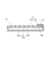
フレクシャ60は、ポリイミド樹脂等で形成された可撓性を有する配線基板61を有しており、この底面にはステンレス鋼等によって形成された薄板状の支持板(図示略)が部分的に張り付けられている。フレクシャ60は、レーザスポット溶接によって支持ビーム部50に接着されている。配線基板61は、その後端側にパッド搭載領域61aを有している。パッド搭載領域61aは、連結板52の突出部52aの上に敷かれる形になる。
The
フレクシャ60のパッド搭載領域61aには、記録用の電極62b,63b、圧電アクチュエータ用の電極64b〜66b、再生用の電極67b,68bが搭載されている。一方、図4の拡大図に示すように、フレクシャ60の先端側には、4つの電極62a,63a,67a,68aが配列されている。また、フレクシャ60の4つの電極62a,63a,67a,68aの後方には、3つの電極64a〜66aが配列されている。電極62a〜68aと電極62b〜68bは、それぞれ配線62c〜68cで電気的に接続されている。各配線62c〜68cは、実際は絶縁膜で覆われている。なお、配線基板61上の配線62c〜68cは、例えばめっき法等の成膜技術によって形成することができる。
In the
電極62a,63aはヘッドスライダ32の記録パッド33,34にそれぞれ接続され、電極67a,68aは再生パッド35,36にそれぞれ接続される。これらの電極同士の接続には、図2に示すようにゴールドボールボンディングが用いられる。
The
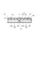
ここで、図4〜図8を参照して、薄膜圧電アクチュエータ70の詳細について説明する。薄膜圧電アクチュエータ70は、伸縮方向が互いに異なるように構成された第1領域70a及び第2領域70bを有している。各領域70a,70bは、PZT等の薄膜の圧電素子で構成されており、その周囲は樹脂膜77によりコーティングされている。尚、薄膜の圧電素子には、厚膜の素子と比較して、軽量、振動に対する周波数特性が良好、設置場所の幅が広い、低電圧で制御可能という様々な利点がある。
Here, the details of the thin
第1領域70aと第2領域70bは、根元付近は樹脂によって一体化されているが、先細りになる先端側は互いに離間している。第1領域70a及び第2領域70bの外側の各辺は並行になっており、対向する内側の辺が外に広がっている。更に、薄膜圧電アクチュエータ70の図中底面側には、それぞれ所定の駆動電圧が印加される電極71a,71b、グランド電位とされる電極71cが設けられている。そして、これらの電極71a,71b,71cは、直接的に、又は、導電部材を介して間接的に、フレクシャ60上の電極66a,64a,65aに電気的に接続される。
The
薄膜圧電アクチュエータ70の電極71a〜71c付近の根元領域は、電極71a,71b,71cと電極66a,64a,65aとが接続されることにより、フレクシャ60の配線基板61に接着される。一方、この根元領域よりも先端側の領域は、フレクシャ60の開口領域に位置するため、ロードビーム53と対面する形になる。
The base regions near the
第1領域70a及び第2領域70bは、図6及び図7に示されるように、薄膜圧電体73と、当該薄膜圧電体73を挟むように配置される第1及び第2の電極膜75a,75bとを含む積層体である。第1領域70aに含まれる第2の電極膜75bと第2領域70bに含まれる第2の電極膜75bとは一体に形成されており、第1領域70aと第2領域70bとの間にも第2の電極膜75bが位置する。この第2の電極膜75bにおける第1領域70aと第2領域70bとの間に位置する部分は、第2の電極膜75bから電極を取り出すための領域となる。なお、第1領域70a及び第2領域70bは、2つの薄膜圧電体が積層配置された2層構造としてもよい。
As shown in FIGS. 6 and 7, the
樹脂膜77は、第1領域70a及び第2領域70b(薄膜圧電体73と第1及び第2の電極膜75a,75bとを含む積層体)を覆うように形成された第1の樹脂膜77aと、電極71a〜71cが形成される領域(薄膜圧電アクチュエータ70の根元領域)に形成される第2の樹脂膜77bとを含んでいる。これにより、樹脂膜77は、電極71a〜71cが形成される領域の厚みが第1領域70a及び第2領域70bの変位する部分に対応する領域の厚みよりも厚くなるように形成されることとなる。樹脂膜77(第1の樹脂膜77a及び第2の樹脂膜77b)の材料には、例えばポリイミド樹脂等を用いることができる。
The
電極71a,71bは、第2の樹脂膜77bの上に形成されると共に、コンタクトホール78a,78bを通して対応する第1電極膜75aに電気的に接続されている。電極71cは、第2の樹脂膜77bの上に形成されると共に、コンタクトホール78cを通して、第2の電極膜75bにおける第1領域70aと第2領域70bとの間に位置する部分に電気的に接続されている。
The
電極71a,71bのそれぞれには、薄膜圧電体73を駆動する駆動電圧が印可される。駆動電圧が印加されると、図8に示されるように、薄膜圧電体73は駆動電圧に対応して矢印A1,A2方向に伸縮する。電極71a,71bにそれぞれ印加される駆動電圧は、例えばバイアス電圧を中心として互いに逆位相となっている。電極71aにバイアス電圧に対しプラスの駆動電圧が印加されると、第1領域70aにおける薄膜圧電体73は矢印A1方向に収縮する。一方、電極71bにバイアス電圧に対しプラスの駆動電圧が印加されると、第2領域70bにおける薄膜圧電体73は矢印A2方向に伸長する。
A driving voltage for driving the thin film
第1領域70a及び第2領域70bは、図14に示されるように、2つの薄膜圧電体が積層配置された2層構造としてもよい。第2の電極膜75bの上には、積層体90が接着剤91により固定されている。積層体90は、薄膜圧電体73と、当該薄膜圧電体73を挟むように配置される第3の電極金属膜75c及び第4の電極金属膜75dとを含んでいる。第2の電極膜75bと第3の電極金属膜75cとが接着剤91で接着されている。
As shown in FIG. 14, the
第1の電極金属膜75a及び第4の電極金属膜75dは、電極71aに電気的に接続されている。第2の電極金属膜75bと第3の電極金属膜75cとは、電極71cに電気的に接続されている。電極71a,71bのそれぞれには、2つの薄膜圧電体73をそれぞれ駆動する駆動電圧が印可される。駆動電圧が印加されると、図14に示されるように、2つの薄膜圧電体73は駆動電圧に対応して矢印A1,A2方向に伸縮する。電極71a,71bにそれぞれ印加される駆動電圧は、例えばバイアス電圧を中心として互いに逆位相となっている。電極71aにバイアス電圧に対しプラスの駆動電圧が印加されると、第1領域70aにおける2つの薄膜圧電体73は矢印A1方向に収縮する。一方、電極71bにバイアス電圧に対しプラスの駆動電圧が印加されると、第2領域70bにおける2つの薄膜圧電体73は矢印A2方向に伸長する。なお、第1領域70a及び第2領域70bは、3つ以上の薄膜圧電体が積層配置された多層構造としてもよい。
The first
伝達板80は、薄膜圧電アクチュエータ70の変位をヘッドスライダ32に伝達する。伝達板80は、一方の面(図4の下面)が薄膜圧電アクチュエータ70に対向し、他方の面がヘッドスライダ32に対向している。伝達板80は、導電性を有する金属、例えばステンレス鋼等によって形成され、図4にも示されるように、幅方向に延びる矩形形状の後部83と、幅細で長尺の連結部84を介して後部83に接続された前部85とを有している。ここで、ヘッドスライダ32、薄膜圧電アクチュエータ70、及び、伝達板80の位置関係を説明する。ヘッドスライダ32は、伝達板80の前部85上に載置されている。薄膜圧電アクチュエータ70は、伝達板80の下に位置しており、電極71a〜71cが位置する根元部分が伝達板80の後部83と重なり、第1領域70a及び第2領域70bの先端部分がそれぞれ前部85と重なるように位置している。
The
次に、図9〜図13を参照して、薄膜圧電アクチュエータ70の製造過程について説明する。図9〜図13の各(a)は、薄膜圧電アクチュエータの製造過程を説明するための模式図である。図9(b)は図9(a)におけるIXb−IXb方向の断面構成を示す模式図である。図10(b)は図10(a)におけるXb−Xb方向の断面構成を示す模式図である。図11(b)は図11(a)におけるXIb−XIb方向の断面構成を示す模式図である。図12(b)は図12(a)におけるXIIb−XIIb方向の断面構成を示す模式図である。図13(b)は図13(a)におけるXIIIb−XIIIb方向の断面構成を示す模式図である。
Next, the manufacturing process of the thin
薄膜圧電アクチュエータ70の形成は、以下の工程(1)〜(5)に従って行う。
The thin
工程(1)
まず、基板Sを用意する。そして、この基板Sの上に、第2の電極膜75bを構成する材料からなる薄膜F1、薄膜圧電体73を構成する材料からなる薄膜F2、及び第1の電極膜75aを構成する材料からなる薄膜F3の順に積層して積層体L1を形成する(図9(a)及び(b)参照)。基板Sには、例えば酸化マグネシア(MgO)を材料とする単結晶基板等を用いることができる。薄膜F1,F3(第1及び第2の電極膜75a,75b)には、例えばPtやIr等の金属の他、導電性酸化物(例えば、IrO等)や導電性樹脂といった導電性材料を用いることができる。薄膜F2には、例えばチタン酸ジルコン酸鉛(PZT)、チタン酸バリウム等の圧電材料を用いることができる。薄膜F1〜F3を形成する方法には、例えばスパッタリング法、CVD法、レーザーアブレーション法等の方法を用いることができる。
Process (1)
First, a substrate S is prepared. On the substrate S, a thin film F1 made of a material constituting the
工程(2)
次に、積層体L1を所望の形状に加工(パターニング)する(図10(a)及び(b)参照)。この工程(2)では、まず、積層体L1上に、第1領域70a、第2領域70c、及び第2の電極膜75bにおける第1領域70aとの第2領域70bとの間に位置する部分に対応する位置にレジスト膜(図示せず)を形成し、当該レジスト膜をマスク層として薄膜F1〜F3をエッチングにより除去する。続いて、上記レジスト膜を除去する。
Process (2)
Next, the laminated body L1 is processed (patterned) into a desired shape (see FIGS. 10A and 10B). In this step (2), first, on the stacked body L1, a portion located between the
次に、第2の電極膜75bにおける第1領域70aとの第2領域70bとの間に位置する部分に対応する開口を有するレジスト膜(図示せず)を再度形成する。そして、このレジスト膜をマスク層として、第2の電極膜75bが露出するまでエッチングする。続いて、上記レジスト膜を除去する。
Next, a resist film (not shown) having an opening corresponding to a portion located between the
以上の工程(1)及び(2)により、基板Sの上に第2の電極膜75b、薄膜圧電体73及び第1の電極膜75aの順に成膜されて、第1領域70a及び第2領域70bが形成されることとなる。
Through the above steps (1) and (2), the
工程(3)
次に、第2の電極膜75b、薄膜圧電体73及び第1の電極膜75aの腐食を回避するために、基板S上において、第1領域70a、第2領域70b、及び第2の電極膜75bにおける第1領域70a及び第2領域70bとの間に位置する部分の表面を覆うように第1の樹脂膜77aを形成する(図11(a)及び(b)参照)。第1の樹脂膜77aは、当該第1の樹脂膜77aを構成する樹脂材料を塗布した後にベークすることにより形成される。
Process (3)
Next, in order to avoid corrosion of the
工程(4)
次に、第1の樹脂膜77a上であって、電極71a〜71cが形成される予定領域(薄膜圧電アクチュエータ70の根元領域)に第2の樹脂膜77bを形成する(図12(a)及び(b)参照)。第2の樹脂膜77bは、第1の樹脂膜77aと同じく、第2の樹脂膜77bを構成する樹脂材料を塗布した後にベークすることにより形成される。
Process (4)
Next, on the
そして、電極71a〜71cに対応する位置に開口を有するレジスト膜(図示せず)を形成する。そして、このレジスト膜をマスク層として樹脂膜77(第1の樹脂膜77a及び第2の樹脂膜77b)をエッチングにより除去し、樹脂膜77にコンタクトホール78a〜78cを形成する(同じく、図12(a)及び(b)参照)。続いて、上記レジスト膜を除去する。
Then, a resist film (not shown) having openings at positions corresponding to the
工程(5)
次に、コンタクトホール78a〜78cに対応する位置に開口を有するレジスト膜(図示せず)を再度形成する。そして、このレジスト膜をマスク層として、コンタクトホール78a〜78cが形成されることにより露出した第1の電極膜75a及び第2の電極膜75b上に、蒸着とリフトオフ法とにより各電極71a〜71cを形成する(図13(a)及び(b)参照)。
Step (5)
Next, a resist film (not shown) having openings at positions corresponding to the contact holes 78a to 78c is formed again. Then, the
その後、基板Sを除去する。これにより、薄膜圧電アクチュエータ70が形成されることとなる。基板Sの除去は、基板SにMgOの単結晶基板を用いる場合、燐酸水溶液(燐酸の濃度が、例えば30%程度である)によりエッチングすることにより行うことができる。なお、エッチング速度を速くするために、燐酸水溶液を予め80℃程度に加熱しておくことが好ましい。
Thereafter, the substrate S is removed. Thereby, the thin
なお、2つの薄膜圧電体が積層配置された2層構造とする場合、積層体L1が形成された基板Sをもう1つ用意し、上記工程(2)の前に、薄膜F3同士が対向するように積層体L1同士を接着剤で接着した後に、一方の基板を除去する工程が追加されることとなる。 In addition, when it is set as the 2 layer structure by which two thin film piezoelectric bodies are laminated | stacked, another board | substrate S with which the laminated body L1 was formed is prepared, and thin film F3 opposes before the said process (2). Thus, after the laminated bodies L1 are bonded to each other with an adhesive, a step of removing one of the substrates is added.
続いて、HGA30の組立て過程の一例を説明する。
Next, an example of the assembly process of the
まず、フレクシャ60をレーザスポット溶接にてロードビーム53に固定する。また、薄膜圧電アクチュエータ70を伝達板80に対して位置決めした後に、これらを接着剤等により固定する。このとき、伝達板80の後部83と薄膜圧電アクチュエータ70の根元部分とを電気絶縁性を有する接着剤等で接着すると共に、第1領域70a及び第2領域70bの先端部分をそれぞれ対応するアーム部86,87に接着剤等で接着する。
First, the
次に、伝達板80が固定された薄膜圧電アクチュエータ70を、電極71a,71b,71cと電極66a,64a,65aとを接続することにより、フレクシャ60に固定する。薄膜圧電アクチュエータ70は電極71a〜71c(電極64a〜66a)の位置でのみフレクシャ60に接続される。したがって、薄膜圧電アクチュエータ70は、ロードビーム53から浮いた状態となっている。次いで、伝達板80の前部85にヘッドスライダ32を接着することにより、本実施形態のHGA30が得られる。
Next, the thin
また、このようにして得られたHGA30にアクチュエータアーム22を連結してヘッドスタックアセンブリ20を構成し、これをハードディスク10上に移動可能に組み立てることで、本実施形態のハードディスク装置1を作製することができる。
Further, the
なお、HGA30の組立て手順は上記のものに限られず、次のような変形例も実施することができる。例えば、薄膜圧電アクチュエータ70をフレクシャ60に接続した後に、伝達板80を薄膜圧電アクチュエータ70に固定するという手順である。また、ヘッドスライダ32、伝達板80、及び薄膜圧電アクチュエータ70を一体に組み立てた後に、これをフレクシャ60上に載せてもよい。
In addition, the assembly procedure of HGA30 is not restricted to the above, The following modifications can also be implemented. For example, the
以上のように、本実施形態によれば、樹脂膜77における電極71a〜71cが形成される領域の厚みが第1領域70a及び第2領域70bの変位する部分に対応する領域の厚みよりも厚いので、第1の電極膜75aと電極71a〜71cとの間隔が比較的大きくなり、第1の電極膜75aと電極71a〜71cとの間の絶縁不良の発生を抑制することができる。また、樹脂膜77における第1領域70a及び第2領域70bの変位する部分に対応する領域の厚みは、上記電極71a〜71cが形成される領域の厚みがより薄くなるので、第1領域70a及び第2領域70b(薄膜圧電体73)の変位が阻害されるようなことはなく、圧電性が低下するのを抑制できる。また、樹脂膜77が硬化する際に生じる応力も小さくなることから、第1領域70a及び第2領域70bが反ってしまうのも抑制できる。
As described above, according to the present embodiment, the thickness of the region of the
また、樹脂層77は、第1領域70a及び第2領域70bを覆うように形成される第1の樹脂膜77aと、電極71a〜71cが形成される領域に形成される第2の樹脂膜77bとを含んでいる。これにより、電極71a〜71cが形成される領域の厚みが第1領域70a及び第2領域70bの変位する部分に対応する領域の厚みよりも厚くされた樹脂膜77を極めて容易に形成することができる。
The
以上、本発明者らによってなされた発明を実施形態に基づき具体的に説明したが、本発明は上記実施形態に限定されるものではない。例えば、薄膜圧電アクチュエータ70の構成は、上述した層構成に限られるものではない。また、記録媒体に対して記録及び再生の双方を行う薄膜磁気ヘッドに代えて、記録又は再生の一方のみを行う薄膜磁気ヘッドを用いてもよい。また、伝達板80を設けることなく、ヘッドスライダ32を薄膜圧電アクチュエータ70に直接搭載するように構成してもよい。また、本発明に係る薄膜圧電体素子は、上述した実施形態のサスペンション及びハードディスク装置以外の電子部品等に適用できる。
As mentioned above, although the invention made by the present inventors has been specifically described based on the embodiment, the present invention is not limited to the above embodiment. For example, the configuration of the thin
また、本実施形態においては、樹脂膜77を第1の樹脂膜77a及び第2の樹脂膜77bで構成することにより、電極71a〜71cが形成される領域の厚みを第1領域70a及び第2領域70bの変位する部分に対応する領域の厚みよりも厚くしているが、樹脂膜77の構成はこれに限られるものではない。例えば、第1領域70a及び第2領域70bの変位する部分に対応する領域を覆うように形成される樹脂膜と、電極71a〜71cが形成される領域に形成される樹脂膜とで構成し、電極71a〜71cが形成される領域に形成される樹脂膜の厚みを第1領域70a及び第2領域70bの変位する部分に対応する領域を覆うように形成される樹脂膜の厚みよりも厚くしてもよい。また、単一の樹脂層77で、電極71a〜71cが形成される領域を厚くするようにしてもよい。更には、第2の樹脂膜77bの上に樹脂膜を更に形成するように構成してもよい。
In the present embodiment, the
1…ハードディスク装置、10…ハードディスク、20…ヘッドスタックアセンブリ、22…アクチュエータアーム、31…薄膜磁気ヘッド、32…ヘッドスライダ、40…サスペンション、50…支持ビーム部、60…フレクシャ、61…配線基板、70…薄膜圧電アクチュエータ(薄膜圧電体素子)、71a〜71c…電極、73…薄膜圧電体、75a…第1の電極膜、75b…第2の電極膜、77…樹脂膜、77a…第1の樹脂膜、77b…第2の樹脂膜、80…伝達板。
DESCRIPTION OF
Claims (9)
前記積層体を覆うように形成される樹脂膜と、
前記樹脂膜上に形成され、前記電極膜に電気的に接続される電極と、を備え、
前記樹脂膜は、前記電極が形成される領域の厚みが前記積層体の変位する部分に対応する領域の厚みよりも厚くなるように形成されていることを特徴とする薄膜圧電体素子。 A laminate including a piezoelectric film and a pair of electrode films disposed so as to sandwich the piezoelectric film;
A resin film formed so as to cover the laminate,
An electrode formed on the resin film and electrically connected to the electrode film,
The thin film piezoelectric element is characterized in that the resin film is formed so that a thickness of a region where the electrode is formed is larger than a thickness of a region corresponding to a portion where the laminate is displaced.
前記新たな積層体は、圧電体膜と、当該圧電体膜を挟むように配置される一対の電極膜とを含むことを特徴とする請求項1に記載の薄膜圧電体素子。 Further comprising a new laminate bonded on the laminate,
2. The thin film piezoelectric element according to claim 1, wherein the new laminate includes a piezoelectric film and a pair of electrode films arranged so as to sandwich the piezoelectric film.
前記ヘッドスライダを当該サスペンションに対して相対的に変位させる薄膜圧電体素子を備え、
前記薄膜圧電体素子は、
圧電体膜と、当該圧電体膜を挟むように配置される一対の電極膜とを含む積層体と、
前記積層体を覆うように形成される樹脂膜と、
前記樹脂膜上に形成され、前記電極膜に電気的に接続される電極と、を有し、
前記樹脂膜は、前記電極が形成される領域の厚みが前記積層体の変位する部分に対応する領域の厚みよりも厚くなるように形成されていることを特徴とするサスペンション。 A suspension on which a head slider having a thin film magnetic head is mounted,
A thin film piezoelectric element for displacing the head slider relative to the suspension;
The thin film piezoelectric element is
A laminate including a piezoelectric film and a pair of electrode films disposed so as to sandwich the piezoelectric film;
A resin film formed so as to cover the laminate,
An electrode formed on the resin film and electrically connected to the electrode film,
The suspension is characterized in that the resin film is formed so that a thickness of a region where the electrode is formed is larger than a thickness of a region corresponding to a portion where the laminate is displaced.
前記新たな積層体は、圧電体膜と、当該圧電体膜を挟むように配置される一対の電極膜とを含むことを特徴とする請求項4に記載のサスペンション。 Further comprising a new laminate bonded on the laminate,
The suspension according to claim 4, wherein the new laminate includes a piezoelectric film and a pair of electrode films arranged so as to sandwich the piezoelectric film.
前記サスペンションは、前記ヘッドスライダを当該サスペンションに対して相対的に変位させる薄膜圧電体素子を有し、
前記薄膜圧電体素子は、
圧電体膜と、当該圧電体膜を挟むように配置される一対の電極膜とを含む積層体と、
前記積層体を覆うように形成される樹脂膜と、
前記樹脂膜上に形成され、前記電極膜に電気的に接続される電極と、を有し、
前記樹脂膜は、前記電極が形成される領域の厚みが前記積層体の変位する部分に対応する領域の厚みよりも厚くなるように形成されていることを特徴とするハードディスク装置。 A recording medium, a head slider having a thin film magnetic head that performs at least one of recording and reproduction with respect to the recording medium, and a suspension on which the head slider is mounted,
The suspension includes a thin film piezoelectric element that displaces the head slider relative to the suspension,
The thin film piezoelectric element is
A laminate including a piezoelectric film and a pair of electrode films disposed so as to sandwich the piezoelectric film;
A resin film formed so as to cover the laminate,
An electrode formed on the resin film and electrically connected to the electrode film,
The hard disk device according to claim 1, wherein the resin film is formed so that a thickness of a region where the electrode is formed is larger than a thickness of a region corresponding to a portion where the stacked body is displaced.
前記新たな積層体は、圧電体膜と、当該圧電体膜を挟むように配置される一対の電極膜とを含むことを特徴とする請求項7に記載のハードディスク装置。
Further comprising a new laminate bonded on the laminate,
8. The hard disk device according to claim 7, wherein the new laminated body includes a piezoelectric film and a pair of electrode films disposed so as to sandwich the piezoelectric film.
Priority Applications (2)
| Application Number | Priority Date | Filing Date | Title |
|---|---|---|---|
| JP2004072989A JP4113143B2 (en) | 2004-03-15 | 2004-03-15 | Thin film piezoelectric element, suspension, and hard disk device |
| US11/054,427 US7183696B2 (en) | 2004-03-15 | 2005-02-10 | Thin film piezoelectric element, suspension assembly, and hard disk drive |
Applications Claiming Priority (1)
| Application Number | Priority Date | Filing Date | Title |
|---|---|---|---|
| JP2004072989A JP4113143B2 (en) | 2004-03-15 | 2004-03-15 | Thin film piezoelectric element, suspension, and hard disk device |
Publications (2)
| Publication Number | Publication Date |
|---|---|
| JP2005260161A JP2005260161A (en) | 2005-09-22 |
| JP4113143B2 true JP4113143B2 (en) | 2008-07-09 |
Family
ID=34918641
Family Applications (1)
| Application Number | Title | Priority Date | Filing Date |
|---|---|---|---|
| JP2004072989A Expired - Lifetime JP4113143B2 (en) | 2004-03-15 | 2004-03-15 | Thin film piezoelectric element, suspension, and hard disk device |
Country Status (2)
| Country | Link |
|---|---|
| US (1) | US7183696B2 (en) |
| JP (1) | JP4113143B2 (en) |
Cited By (3)
| Publication number | Priority date | Publication date | Assignee | Title |
|---|---|---|---|---|
| US8038515B2 (en) | 2004-07-23 | 2011-10-18 | Oy Halton Group Ltd. | Control of exhaust systems |
| US10082299B2 (en) | 2008-12-03 | 2018-09-25 | Oy Halton Group Ltd. | Exhaust flow control system and method |
| JP7333435B1 (en) | 2022-02-18 | 2023-08-24 | 本田技研工業株式会社 | Pouring device and its manufacturing method |
Families Citing this family (9)
| Publication number | Priority date | Publication date | Assignee | Title |
|---|---|---|---|---|
| CN1828727A (en) * | 2005-02-28 | 2006-09-06 | 新科实业有限公司 | Micro driver and its magnetic head tab combination and magnetic disk driving unit |
| JP5032949B2 (en) * | 2007-11-14 | 2012-09-26 | エイチジーエスティーネザーランドビーブイ | Microactuator, head gimbal assembly and disk drive device |
| US8677607B2 (en) | 2008-03-07 | 2014-03-25 | Tdk Corporation | Method of manufacturing magnetoresistive element |
| JP5943590B2 (en) * | 2011-01-07 | 2016-07-05 | 日本発條株式会社 | Piezoelectric element manufacturing method, piezoelectric element, piezoelectric actuator, and head suspension |
| JP5592289B2 (en) * | 2011-02-25 | 2014-09-17 | Tdk株式会社 | Piezoelectric element, manufacturing method thereof, and head gimbal assembly equipped with the piezoelectric element |
| US9875759B1 (en) | 2015-09-10 | 2018-01-23 | Magnecomp Corporation | Dual stage actuated suspension having shear-mode PZT actuators for rotating gimbal tongue |
| CN112520685B (en) * | 2020-12-04 | 2024-03-01 | 青岛大学 | Double-layer film actuator and preparation method thereof |
| US20220415347A1 (en) * | 2021-06-29 | 2022-12-29 | Seagate Technology Llc | Low force actuator with a coupler piece and constrained layer construction |
| JP2023128424A (en) * | 2022-03-03 | 2023-09-14 | 日本発條株式会社 | Suspension for disk device |
Family Cites Families (11)
| Publication number | Priority date | Publication date | Assignee | Title |
|---|---|---|---|---|
| US2266768A (en) * | 1941-03-08 | 1941-12-23 | Brush Dev Co | Means and method for protecting piezoelectric units |
| JP3441429B2 (en) | 2000-10-20 | 2003-09-02 | 松下電器産業株式会社 | Piezoelectric actuator, method of manufacturing the same, and method of driving piezoelectric actuator |
| SG147277A1 (en) | 2000-02-01 | 2008-11-28 | Matsushita Electric Ind Co Ltd | Head support mechanism and thin film piezoelectric actuator |
| US6617762B2 (en) * | 2000-08-03 | 2003-09-09 | Nec Tokin Ceramics Corporation | Microactuator device with a countermeasure for particles on a cut face thereof |
| JP4101492B2 (en) | 2000-10-23 | 2008-06-18 | 松下電器産業株式会社 | Head support mechanism |
| JP2002203998A (en) * | 2000-12-28 | 2002-07-19 | Denso Corp | Piezoelectric-substance element and the manufacturing method thereof |
| US6903491B2 (en) * | 2001-04-26 | 2005-06-07 | Matsushita Electric Industrial Co., Ltd. | Piezoelectric element, actuator, and inkjet head |
| JP2003061371A (en) * | 2001-08-10 | 2003-02-28 | Fujitsu Ltd | Piezoelectric actuator |
| SG103367A1 (en) * | 2001-11-02 | 2004-04-29 | Matsushita Electric Ind Co Ltd | Piezoelectric driving device |
| JP3846271B2 (en) * | 2001-11-05 | 2006-11-15 | 松下電器産業株式会社 | Thin film piezoelectric element and manufacturing method thereof |
| JP4305016B2 (en) * | 2002-03-18 | 2009-07-29 | セイコーエプソン株式会社 | Piezoelectric actuator unit and liquid jet head using the same |
-
2004
- 2004-03-15 JP JP2004072989A patent/JP4113143B2/en not_active Expired - Lifetime
-
2005
- 2005-02-10 US US11/054,427 patent/US7183696B2/en active Active
Cited By (3)
| Publication number | Priority date | Publication date | Assignee | Title |
|---|---|---|---|---|
| US8038515B2 (en) | 2004-07-23 | 2011-10-18 | Oy Halton Group Ltd. | Control of exhaust systems |
| US10082299B2 (en) | 2008-12-03 | 2018-09-25 | Oy Halton Group Ltd. | Exhaust flow control system and method |
| JP7333435B1 (en) | 2022-02-18 | 2023-08-24 | 本田技研工業株式会社 | Pouring device and its manufacturing method |
Also Published As
| Publication number | Publication date |
|---|---|
| JP2005260161A (en) | 2005-09-22 |
| US20050200237A1 (en) | 2005-09-15 |
| US7183696B2 (en) | 2007-02-27 |
Similar Documents
| Publication | Publication Date | Title |
|---|---|---|
| US7183696B2 (en) | Thin film piezoelectric element, suspension assembly, and hard disk drive | |
| US7420785B2 (en) | Suspension assembly, hard disk drive, and method of manufacturing suspension assembly | |
| JP7145771B2 (en) | Multilayer microactuator for hard disk drive suspension | |
| US8189301B2 (en) | Wireless microactuator motor assembly for use in a hard disk drive suspension, and mechanical and electrical connections thereto | |
| JP4897767B2 (en) | Thin-film piezoelectric element, manufacturing method thereof, head gimbal assembly using the same, and hard disk drive using the head gimbal assembly | |
| US20090086379A1 (en) | Head suspension and piezoelectric actuator | |
| JP2006244690A (en) | Rotatable piezoelectric micro actuator, and head gimbal assembly, and disk drive unit | |
| JP2006244691A (en) | Micro-actuator, head gimbal assembly and disk drive using the same | |
| JP6054593B2 (en) | Electrical connection structure of piezoelectric element | |
| US11348609B2 (en) | Head suspension assembly and disk device | |
| US11694715B2 (en) | Head suspension assembly and disk device | |
| JP2001332041A (en) | Thin film piezoelectric body actuator for disk device and its manufacturing method | |
| JP6067347B2 (en) | Manufacturing method of head gimbal assembly, manufacturing method of flexure constituting the same, and flexure sheet used for manufacturing head gimbal assembly and flexure | |
| JP2008034091A (en) | Microactuator, head gimbal assembly with microactuator, and method of manufacturing head gimbal assembly | |
| JP2007149327A (en) | Micro-actuator, head gimbal assembly and disk drive using the same | |
| WO2000030081A1 (en) | Record/reproduce head support mechanism and record/reproduce apparatus | |
| US7518833B2 (en) | Micro-actuator with electric spark preventing structure, HGA, and disk drive unit with the same, and manufacturing method thereof | |
| JP6096637B2 (en) | Head gimbal assembly and disk device provided with the same | |
| US20080273272A1 (en) | Micro-Actuator, HGA Equipped with the Micro-Actuator and Method for Manufacturing the HGA | |
| JP4071203B2 (en) | Method for bonding thin film piezoelectric element | |
| JP2007095275A (en) | Micro-actuator provided with electric spark preventing structure, magnetic head assembly and disk device using it and manufacturing method of micro-actuator | |
| JP4581447B2 (en) | Method for manufacturing thin film piezoelectric element and method for manufacturing suspension | |
| JP4167191B2 (en) | Suspension, head gimbal assembly, and hard disk drive | |
| JP5303776B2 (en) | Suspension, head gimbal assembly, method for manufacturing the same, and magnetic disk drive unit | |
| JP4197654B2 (en) | Head gimbal assembly and hard disk device |
Legal Events
| Date | Code | Title | Description |
|---|---|---|---|
| A977 | Report on retrieval |
Free format text: JAPANESE INTERMEDIATE CODE: A971007 Effective date: 20060417 |
|
| TRDD | Decision of grant or rejection written | ||
| A01 | Written decision to grant a patent or to grant a registration (utility model) |
Free format text: JAPANESE INTERMEDIATE CODE: A01 Effective date: 20080408 |
|
| A61 | First payment of annual fees (during grant procedure) |
Free format text: JAPANESE INTERMEDIATE CODE: A61 Effective date: 20080410 |
|
| R150 | Certificate of patent or registration of utility model |
Ref document number: 4113143 Country of ref document: JP Free format text: JAPANESE INTERMEDIATE CODE: R150 Free format text: JAPANESE INTERMEDIATE CODE: R150 |
|
| FPAY | Renewal fee payment (event date is renewal date of database) |
Free format text: PAYMENT UNTIL: 20110418 Year of fee payment: 3 |
|
| FPAY | Renewal fee payment (event date is renewal date of database) |
Free format text: PAYMENT UNTIL: 20110418 Year of fee payment: 3 |
|
| FPAY | Renewal fee payment (event date is renewal date of database) |
Free format text: PAYMENT UNTIL: 20120418 Year of fee payment: 4 |
|
| FPAY | Renewal fee payment (event date is renewal date of database) |
Free format text: PAYMENT UNTIL: 20130418 Year of fee payment: 5 |
|
| FPAY | Renewal fee payment (event date is renewal date of database) |
Free format text: PAYMENT UNTIL: 20140418 Year of fee payment: 6 |