JP5032949B2 - Microactuator, head gimbal assembly and disk drive device - Google Patents
Microactuator, head gimbal assembly and disk drive device Download PDFInfo
- Publication number
- JP5032949B2 JP5032949B2 JP2007296152A JP2007296152A JP5032949B2 JP 5032949 B2 JP5032949 B2 JP 5032949B2 JP 2007296152 A JP2007296152 A JP 2007296152A JP 2007296152 A JP2007296152 A JP 2007296152A JP 5032949 B2 JP5032949 B2 JP 5032949B2
- Authority
- JP
- Japan
- Prior art keywords
- silicon substrate
- head slider
- fixed
- head
- path
- Prior art date
- Legal status (The legal status is an assumption and is not a legal conclusion. Google has not performed a legal analysis and makes no representation as to the accuracy of the status listed.)
- Active
Links
Images


Classifications
-
- G—PHYSICS
- G11—INFORMATION STORAGE
- G11B—INFORMATION STORAGE BASED ON RELATIVE MOVEMENT BETWEEN RECORD CARRIER AND TRANSDUCER
- G11B5/00—Recording by magnetisation or demagnetisation of a record carrier; Reproducing by magnetic means; Record carriers therefor
- G11B5/48—Disposition or mounting of heads or head supports relative to record carriers ; arrangements of heads, e.g. for scanning the record carrier to increase the relative speed
- G11B5/4806—Disposition or mounting of heads or head supports relative to record carriers ; arrangements of heads, e.g. for scanning the record carrier to increase the relative speed specially adapted for disk drive assemblies, e.g. assembly prior to operation, hard or flexible disk drives
- G11B5/4826—Mounting, aligning or attachment of the transducer head relative to the arm assembly, e.g. slider holding members, gimbals, adhesive
-
- G—PHYSICS
- G11—INFORMATION STORAGE
- G11B—INFORMATION STORAGE BASED ON RELATIVE MOVEMENT BETWEEN RECORD CARRIER AND TRANSDUCER
- G11B5/00—Recording by magnetisation or demagnetisation of a record carrier; Reproducing by magnetic means; Record carriers therefor
- G11B5/48—Disposition or mounting of heads or head supports relative to record carriers ; arrangements of heads, e.g. for scanning the record carrier to increase the relative speed
- G11B5/4806—Disposition or mounting of heads or head supports relative to record carriers ; arrangements of heads, e.g. for scanning the record carrier to increase the relative speed specially adapted for disk drive assemblies, e.g. assembly prior to operation, hard or flexible disk drives
- G11B5/4873—Disposition or mounting of heads or head supports relative to record carriers ; arrangements of heads, e.g. for scanning the record carrier to increase the relative speed specially adapted for disk drive assemblies, e.g. assembly prior to operation, hard or flexible disk drives the arm comprising piezoelectric or other actuators for adjustment of the arm
-
- G—PHYSICS
- G11—INFORMATION STORAGE
- G11B—INFORMATION STORAGE BASED ON RELATIVE MOVEMENT BETWEEN RECORD CARRIER AND TRANSDUCER
- G11B5/00—Recording by magnetisation or demagnetisation of a record carrier; Reproducing by magnetic means; Record carriers therefor
- G11B5/48—Disposition or mounting of heads or head supports relative to record carriers ; arrangements of heads, e.g. for scanning the record carrier to increase the relative speed
- G11B5/54—Disposition or mounting of heads or head supports relative to record carriers ; arrangements of heads, e.g. for scanning the record carrier to increase the relative speed with provision for moving the head into or out of its operative position or across tracks
- G11B5/55—Track change, selection or acquisition by displacement of the head
- G11B5/5521—Track change, selection or acquisition by displacement of the head across disk tracks
- G11B5/5552—Track change, selection or acquisition by displacement of the head across disk tracks using fine positioning means for track acquisition separate from the coarse (e.g. track changing) positioning means
Landscapes
- Supporting Of Heads In Record-Carrier Devices (AREA)
- Moving Of The Head To Find And Align With The Track (AREA)
- Adjustment Of The Magnetic Head Position Track Following On Tapes (AREA)
Description
本発明は、マイクロアクチュエータ、ヘッド・ジンバル・アセンブリ及びディスク・ドライブ装置に関し、特に、マイクロアクチュエータ上に固定されるヘッド・スライダの接地に関する。 The present invention relates to a microactuator, a head gimbal assembly, and a disk drive device, and more particularly to grounding a head slider fixed on the microactuator.
ディスク・ドライブ装置として、光ディスク、光磁気ディスク、あるいはフレキシブル磁気ディスクなどの様々な態様の記録ディスクを使用する装置が知られているが、その中で、ハードディスク・ドライブ(HDD)は、コンピュータの記憶装置として広く普及し、現在のコンピュータ・システムにおいて欠かすことができない記憶装置の一つとなっている。この他、動画像記録再生装置、カーナビゲーション・システム、あるいは携帯電話など、HDDの用途は、その優れた特性により益々拡大している。 As a disk drive device, a device using a recording disk of various modes such as an optical disk, a magneto-optical disk, or a flexible magnetic disk is known. Among them, a hard disk drive (HDD) is a memory of a computer. It has become widespread as a device, and has become one of the storage devices indispensable in current computer systems. In addition, the applications of HDDs such as moving image recording / reproducing devices, car navigation systems, and mobile phones are increasing more and more due to their excellent characteristics.
HDDで使用される磁気ディスクは、同心円状に形成された複数のデータ・トラックと複数のサーボ・トラックとを有している。各データ・トラックには、ユーザ・データを含む複数のデータ・セクタが記録されている。各サーボ・トラックはアドレス情報を有する。サーボ・トラックは、円周方向において離間して配置された複数のサーボ・データによって構成されており、各サーボ・データの間に1もしくは複数のデータ・セクタが記録されている。ヘッド素子部がサーボ・データのアドレス情報に従って所望のデータ・セクタにアクセスすることによって、データ・セクタへのデータ書き込み及びデータ・セクタからのデータ読み出しを行うことができる。 A magnetic disk used in the HDD has a plurality of data tracks and a plurality of servo tracks formed concentrically. Each data track is recorded with a plurality of data sectors including user data. Each servo track has address information. The servo track is composed of a plurality of servo data spaced apart in the circumferential direction, and one or a plurality of data sectors are recorded between each servo data. When the head element unit accesses a desired data sector according to the address information of the servo data, data writing to the data sector and data reading from the data sector can be performed.
ヘッド素子部はスライダ上に形成されており、さらにそのスライダはアクチュエータのサスペンション上に固着されている。アクチュエータとヘッド・スライダのアセンブリを、ヘッド・スタック・アセンブリ(HSA)と呼ぶ。また、サスペンションとヘッド・スライダのアセンブリを、ヘッド・ジンバル・アセンブリ(HGA)と呼ぶ。磁気ディスクに対向するスライダABS(Air Bearing Surface)面と回転している磁気ディスクとの間の空気の粘性による圧力が、サスペンションによって磁気ディスク方向に加えられる圧力とバランスすることによって、ヘッド・スライダは磁気ディスク上を一定のギャップを置いて浮上することができる。アクチュエータが回動軸を中心に回動することによって、ヘッド・スライダを目的のトラックへ移動すると共に、そのトラック上に位置決めする。 The head element portion is formed on a slider, and the slider is fixed on the suspension of the actuator. The assembly of the actuator and the head slider is called a head stack assembly (HSA). The assembly of the suspension and the head slider is called a head gimbal assembly (HGA). The head slider is formed by balancing the pressure due to the viscosity of the air between the slider ABS (Air Bearing Surface) facing the magnetic disk and the rotating magnetic disk with the pressure applied to the magnetic disk by the suspension. It can float on the magnetic disk with a certain gap. As the actuator rotates about the rotation axis, the head slider moves to the target track and is positioned on the track.
磁気ディスクのTPI(Track Per Inch)の増加に従い、ヘッド・スライダの位置決め精度の向上が求められている。しかし、VCM(Voice Coil Motor)によるアクチュエータの駆動は、その位置決め精度に限界が存在する。そのため、アクチュエータの先端に小型のアクチュエータ(マイクロアクチュエータ)を実装し、より精細な位置決めを行う技術が提案されている(例えば特許文献1を参照)。 As the TPI (Track Per Inch) of a magnetic disk increases, improvement in head / slider positioning accuracy is required. However, actuator driving by VCM (Voice Coil Motor) has a limit in positioning accuracy. For this reason, a technique has been proposed in which a small actuator (microactuator) is mounted on the tip of the actuator to perform finer positioning (see, for example, Patent Document 1).
また、磁気ディスクには、外来電磁波やスピンドル・モータが生成するノイズによる電荷が帯電している。磁気ディスクとヘッド・スライダとはキャパシタンスを構成しているため、高い周波数において、ヘッド・スライダに電荷が誘導される。ヘッド・スライダに帯電した電荷の静電放電(ESD)によるヘッド素子部の損傷を避けるため、ヘッド・スライダのスライダ本体は、接地されていることが必要となる。ヘッド・スライダがマイクロアクチュエータ上に固定されている場合、ヘッド・スライダを、マイクロアクチュエータを介して接地することが必要となる(例えば特許文献2を参照)。
様々なマイクロアクチュエータ構造が提案されている中で、上記先行技術文献に開示されているように、マイクロエレクトロメカニカルシステム(MEMS)を有し、ヘッド・スライダを直接微動させるマイクロアクチュエータは、変位量の大きさと共振周波数の高さから、ヘッド・スライダの位置決め性能を高めるのに有利である。また、MEMSの基板は、その加工のためにシリコンで形成されている。シリコンの導電率はおよそ2.52E−4[S/m]であり、ESDを防ぐために必要十分な抵抗値を有している。 Various microactuator structures have been proposed. As disclosed in the prior art document, a microactuator having a microelectromechanical system (MEMS) and finely moving a head slider directly has a displacement amount. From the size and the high resonance frequency, it is advantageous to improve the positioning performance of the head slider. A MEMS substrate is formed of silicon for processing. The conductivity of silicon is approximately 2.52E-4 [S / m], and has a necessary and sufficient resistance value to prevent ESD.
一方、TPI及びBPI(Bit Per Inch)の増加及びヘッド素子部の小型化が進むにつれ、ヘッド素子部の出力信号レベルも小さくなってきている。このため、ヘッド素子部は、ノイズの影響をより受けやすくなってきている。磁気ディスクからヘッド・スライダに誘導されたノイズは、ヘッド素子部の再生系に入り込み、再生信号に大きな影響を及ぼす。このノイズの発生を抑えるためには、ヘッド・スライダのノイズを、接地ラインを通してサスペンションに迅速に逃がすことが効果的である。 On the other hand, as TPI and BPI (Bit Per Inch) increase and the size of the head element portion progresses, the output signal level of the head element portion also decreases. For this reason, the head element section is more susceptible to noise. Noise induced from the magnetic disk to the head slider enters the reproduction system of the head element unit and greatly affects the reproduction signal. In order to suppress the generation of this noise, it is effective to quickly release the head slider noise to the suspension through the ground line.
上述のように、シリコンの導電率は、ESDを防ぐためには十分に高い値である。しかし、その導電率は、ヘッド・スライダに誘導されたノイズを接地レベルに逃がすためには十分ではない。従って、ヘッド・スライダが固定されるシリコン基板を有するマイクロアクチュエータにおいて、ヘッド・スライダの誘導ノイズをサスペンションに逃がして、ヘッド・スライダを常に接地電位に維持するための構造が要求される。 As described above, the conductivity of silicon is sufficiently high to prevent ESD. However, its conductivity is not sufficient to allow the noise induced in the head slider to escape to ground level. Therefore, in a microactuator having a silicon substrate to which the head slider is fixed, a structure is required for allowing the head slider to be always kept at the ground potential by letting the head slider inductive noise escape to the suspension.
本発明の一態様に係るヘッド・ジンバル・アセンブリは、サスペンションと、前記サスペンション上に固定され、可動部と固定部とを有するシリコン基板と、前記シリコン基板上に固定されている圧電素子と、前記可動部上に固定されているヘッド・スライダと、前記シリコン基板上に形成されており、前記シリコン基板よりも導電率が大きく、前記ヘッド・スライダの電荷を伝送する、電導路と、前記サスペンション上に形成され、前記ヘッド・スライダが載置されているヘッド・スライダ載置面の反対面において前記シリコン基板上の前記電導路に接触している導電スタッドを有する。電導路により、マイクロアクチュエータのシリコン基板上に固定されているヘッド・スライダのノイズを、効果的にサスペンションに逃がすことができる。 A head gimbal assembly according to an aspect of the present invention includes a suspension, a silicon substrate fixed on the suspension and having a movable part and a fixed part, a piezoelectric element fixed on the silicon substrate, A head slider fixed on the movable portion; and a conductive path formed on the silicon substrate, having a conductivity higher than that of the silicon substrate and transmitting charges of the head slider; and on the suspension And a conductive stud in contact with the conductive path on the silicon substrate on the opposite surface of the head slider mounting surface on which the head slider is mounted. By the electric conduction path, the noise of the head slider fixed on the silicon substrate of the microactuator can be effectively released to the suspension.
前記電導路は、不純物含有シリコン層を有することが好ましい。これにより、シリコン基板の動きを妨げることなく電導路を形成することができる。さらに、前記電導路は、前記スライダ載置面上で前記可動部から前記固定部まで延在している不純物含有シリコン層を有することが好ましい。 The conductive path preferably has an impurity-containing silicon layer. Thereby, a conductive path can be formed without hindering the movement of the silicon substrate. Further, it is preferable that the conductive path has an impurity-containing silicon layer extending from the movable part to the fixed part on the slider mounting surface.
前記電導路は、前記シリコン基板を貫通して前記ヘッド・スライダ載置面から前記反対面に延びる貫通路を有することが好ましい。これにより、シリコン基板上の配線を避けることができ、マイクロアクチュエータの製造を効率化することができる。前記電導路は、前記スライダ載置面上で延在して前記貫通路とつながっている不純物含有シリコン層を有することが好ましい。これにより、可動部の動きへの影響を小さくすることができる。前記シリコン基板は複数のスルーホールを有し、前記電導路は、前記複数のスルーホールのそれぞれを通る貫通路を有する。これにより、可動部の動きへの影響を小さくすることができる。 The conductive path preferably has a through path that extends through the silicon substrate from the head slider mounting surface to the opposite surface. Thereby, the wiring on the silicon substrate can be avoided, and the production of the microactuator can be made efficient. The conductive path preferably has an impurity-containing silicon layer that extends on the slider mounting surface and is connected to the through path. Thereby, the influence on the motion of the movable part can be reduced. The silicon substrate has a plurality of through holes, and the conductive path has a through path that passes through each of the plurality of through holes. Thereby, the influence on the motion of the movable part can be reduced.
前記シリコン基板は、スルーホールを有し、前記貫通路は、前記スルーホールを貫通していることが好ましい。これにより、スルーホールに導電層を形成することで、容易に電導路の一部を形成することができる。前記貫通路は、前記スルーホール内に付着された金属層を有することで、導電率を大きくすることができる。あるいは、前記貫通路は、前記スルーホールの内面上に形成された不純物含有シリコン層を有することで、製造効率をあげることができる。好ましくは、前記スルーホールは前記固定部に形成されている。これにより、スルーホールが可動部の動きを損なうことを避けることができる。 Preferably, the silicon substrate has a through hole, and the through path passes through the through hole. Thus, a part of the conductive path can be easily formed by forming the conductive layer in the through hole. The through path has a metal layer attached in the through hole, so that the conductivity can be increased. Alternatively, the through path has an impurity-containing silicon layer formed on the inner surface of the through hole, so that the production efficiency can be increased. Preferably, the through hole is formed in the fixed portion. Thereby, it can avoid that a through hole impairs the movement of a movable part.
本発明の他の態様に係る、マイクロアクチュエータは、サスペンションに固定される固定部と、ヘッド・スライダが固定される可動部を有するシリコン基板と、前記シリコン基板上に固定され、前記可動部を動かす圧電素子と、前記シリコン基板上に形成されており、前記シリコン基板よりも導電率が大きく、前記スライダが載置されるスライダ載置面からのその反対面に延びる電導路とを有する。電導路により、マイクロアクチュエータのシリコン基板上に固定されているヘッド・スライダのノイズを、効果的にサスペンションに逃がすことができる。 According to another aspect of the present invention, a microactuator includes a fixed portion fixed to a suspension, a silicon substrate having a movable portion to which a head slider is fixed, and the movable portion fixed on the silicon substrate and moving the movable portion. A piezoelectric element and a conductive path that is formed on the silicon substrate, has a higher conductivity than the silicon substrate, and extends on the opposite surface from the slider mounting surface on which the slider is mounted. By the electric conduction path, the noise of the head slider fixed on the silicon substrate of the microactuator can be effectively released to the suspension.
本発明の他の態様に係る、ディスク・ドライブ装置は、筐体と、前記筐体内に実装され、ディスクを回転するモータと、前記ディスクにアクセスするヘッド・スライダと、前記ヘッド・スライダを保持し、前記ディスク上で前記ヘッド・スライダを半径方向に移動するアクチュエータとを有する。前記アクチュエータは、導電スタッドを有するサスペンションと、前記ヘッド・スライダが載置されているヘッド・スライダ載置面を有し、前記ヘッド・スライダ載置面の反対面において前記導電スタッドと接触して前記サスペンションに固定されている、マイクロアクチュエータとを有する。前記マイクロアクチュエータは、前記ヘッド・スライダが固定されている可動部と、前記導電スタッドと接触して前記サスペンションに固定されている固定部と、を有するシリコン基板と、前記シリコン基板上に固定され、前記可動部を動かす圧電素子と、前記シリコン基板上に形成されており、前記シリコン基板よりも導電率が大きく、前記ヘッド・スライダの電荷を前記導電スタッドに伝送する、電導路とを有する。電導路により、マイクロアクチュエータのシリコン基板上に固定されているヘッド・スライダのノイズを、効果的にサスペンションに逃がすことができる。 According to another aspect of the present invention, a disk drive device includes a housing, a motor mounted in the housing, for rotating the disk, a head slider for accessing the disk, and the head slider. And an actuator for moving the head slider on the disk in a radial direction. The actuator includes a suspension having a conductive stud, and a head slider mounting surface on which the head slider is mounted, and contacts the conductive stud on the opposite surface of the head slider mounting surface. And a microactuator fixed to the suspension. The microactuator is fixed on the silicon substrate, a silicon substrate having a movable part to which the head slider is fixed, a fixed part that is fixed to the suspension in contact with the conductive stud, A piezoelectric element that moves the movable part, and a conductive path that is formed on the silicon substrate, has a higher conductivity than the silicon substrate, and transmits the charge of the head slider to the conductive stud. By the electric conduction path, the noise of the head slider fixed on the silicon substrate of the microactuator can be effectively released to the suspension.
本発明によれば、マイクロアクチュエータのシリコン基板上に固定されているヘッド・スライダのノイズを、効果的にグランドに逃がすことができる。 According to the present invention, the noise of the head slider fixed on the silicon substrate of the microactuator can be effectively released to the ground.
以下に、本発明の好ましい実施の形態を説明する。説明の明確化のため、以下の記載及び図面は、適宜、省略及び簡略化がなされている。又、各図面において、同一要素には同一の符号が付されており、説明の明確化のため、必要に応じて重複説明は省略されている。本実施形態においては、ディスク・ドライブ装置の一例として、ハードディスク・ドライブ(HDD)について説明する。 The preferred embodiments of the present invention will be described below. For clarity of explanation, the following description and drawings are omitted and simplified as appropriate. Moreover, in each drawing, the same code | symbol is attached | subjected to the same element and the duplication description is abbreviate | omitted as needed for clarification of description. In this embodiment, a hard disk drive (HDD) will be described as an example of a disk drive device.
本形態のHDDに実装されるヘッド・ジンバル・アセンブリ(HGA)は、サスペンションとヘッド・スライダに加えて、マイクロアクチュエータを有する。本形態のマイクロアクチュエータはマイクロエレクトロメカニカルシステム(MEMS)を有し、可動部を含むシリコン基板を有している。シリコン基板上に圧電素子が固定され、圧電素子の伸縮に応じてシリコン基板の可動部が動く。ヘッド・スライダは可動部に固定されている。この可動部の動きによってヘッド・スライダが微動し、ヘッド・スライダの精細な位置決めを行うことができる。 A head gimbal assembly (HGA) mounted on the HDD of this embodiment has a microactuator in addition to a suspension and a head slider. The microactuator of this embodiment has a microelectromechanical system (MEMS) and a silicon substrate including a movable part. A piezoelectric element is fixed on the silicon substrate, and the movable part of the silicon substrate moves according to the expansion and contraction of the piezoelectric element. The head slider is fixed to the movable part. The head slider is finely moved by the movement of the movable portion, and the head slider can be precisely positioned.
本形態のマイクロアクチュエータは、シリコン基板上に形成された電導路を有している。この電導路は、ヘッド・スライダの帯電電荷をサスペンションへ伝送する。電導路の導電率はシリコン基板の導電率よりも大きく、ヘッド・スライダのノイズ電荷を迅速にサスペンションに逃がすことができる。これにより、ヘッド素子部の静電放電(ESD)破壊を防止すると共に、再生系へのノイズ混入を効果的に抑えることができる。 The microactuator of this embodiment has a conductive path formed on a silicon substrate. This conductive path transmits the charged electric charge of the head slider to the suspension. The conductivity of the conductive path is larger than that of the silicon substrate, and the noise charge of the head slider can be quickly released to the suspension. Thereby, electrostatic discharge (ESD) destruction of the head element portion can be prevented, and noise mixing in the reproduction system can be effectively suppressed.
本形態のヘッド・ジンバル・アセンブリ(HGA)について説明を行う前に、図1を参照して、HDDの全体構成について説明を行う。HDD1の機構的構成要素は、ベース102内に収容されている。ベース102内の各構成要素の制御は、ベース外に固定された回路基板上の制御回路(不図示)が行う。HDD1は、データを記憶するディスクである磁気ディスク101と、磁気ディスク101にアクセス(リードあるいはライト)するヘッド・スライダ105を有している。ヘッド・スライダ105は、ユーザ・データの磁気ディスク101への書き込み及び/又は読み出しを行うヘッド素子部と、そのヘッド素子部がその面上に形成されているスライダとを備えている。
Before describing the head gimbal assembly (HGA) of this embodiment, the overall configuration of the HDD will be described with reference to FIG. The mechanical components of the HDD 1 are accommodated in the
アクチュエータ106は、ヘッド・スライダ105を保持している。磁気ディスク101へのアクセスのため、アクチュエータ106は回動軸107を中心に回動することで、回転している磁気ディスク101上でヘッド・スライダ105を移動する。駆動機構としてのボイス・コイル・モータ(VCM)109は、アクチュエータ106を駆動する。アクチュエータ106及びVCM109のアセンブリは、ヘッド・スライダ105の移動機構である。アクチュエータ106は、ヘッド・スライダ105が配置された長手方向におけるその先端部から、サスペンション110、アーム111、コイル・サポート112及びVCMコイル113の順で結合された各構成部材を備えている。
The
ベース102に固定されたスピンドル・モータ(SPM)103は、所定の角速度で磁気ディスク101を回転する。磁気ディスク101に対向するスライダのABS(Air Bearing Surface)面と回転している磁気ディスク101との間の空気の粘性による圧力が、サスペンション110によって磁気ディスク101方向に加えられる圧力とバランスすることによって、ヘッド・スライダ105は磁気ディスク101上を浮上する。
A spindle motor (SPM) 103 fixed to the
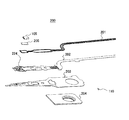
図2は、本形態のHGA200の各構成要素を示す分解斜視図である。HGA200は、サスペンション110、マイクロアクチュエータ205及びヘッド・スライダ105を有している。サスペンション110は、フレックス・ケーブル201、ジンバル202、ロード・ビーム203及びマウント・プレート204を有している。ロード・ビーム203は、精密な薄板バネとして、ステンレス鋼などによって形成される。その剛性はジンバル202よりも高い。ロード・ビーム203は、バネ性を有することによってヘッド・スライダ105への荷重を発生させる。
FIG. 2 is an exploded perspective view showing each component of the
マウント・プレート204及びジンバル202は、例えば、ステンレス鋼で形成する。ジンバル202は、ジンバル・タング224を有しており、マイクロアクチュエータ205とヘッド・スライダ105とは、このジンバル・タング224上に固定される。ジンバル・タング224は弾性的に支持されており、マイクロアクチュエータ205及びヘッド・スライダ105を保持すると共に、自由に傾くことによってヘッド・スライダ105の姿勢制御に寄与する。フレックス・ケーブル201の一端の各端子はマイクロアクチュエータ205及びヘッド・スライダ105に接続され、他端の端子はアクチュエータ106に固定される基板に接続される。フレックス・ケーブル201は、リード信号やライト信号の他、マイクロアクチュエータ205を制御する制御信号を伝送する。
The
図3は、本形態のマイクロアクチュエータ205の構造を模式的に示す分解斜視図である。マイクロアクチュエータ205は、MEMS251と圧電素子252とから構成されている。圧電素子252は、MEMS251上において、ヘッド・スライダ105と同一の面上に固定される。本例においては、圧電素子252は、MEMS251のディスク対抗面上において、ヘッド・スライダ105のリーディング側に固定される。
FIG. 3 is an exploded perspective view schematically showing the structure of the
図4は、MEMS251の構造を模式的に示す分解斜視図である。MEMS251は、シリコン基板253と、シリコン基板253上にメッキあるいはスパッタにより形成される金属層254とを有している。金属層254は、典型的には、金により形成される。また、シリコン基板253と金属層254との間には、下地層255がメッキあるいはスパッタにより形成される。下地層255は、典型的には、金属層254と同様の金属である。金属層254は、複数の部分から構成されている。プラットフォーム540は、主板541上にスタッド542a〜542cを有している。ヘッド・スライダ105はこれらスタッド542a〜542cに接触して、プラットフォーム540上に接着剤で固定される。プラットフォーム540は、ヘッド・スライダ105を接地するための電導路の一部を構成する。この点については後述する。
FIG. 4 is an exploded perspective view schematically showing the structure of the
接続パッド543a〜543fは、ヘッド・スライダ105の接続パッドと電気的に接続され、ヘッド素子部などの素子に信号を伝送する。接続パッド544a〜544iは、フレックス・ケーブル201の接続パッドと電気的に接続される。圧電素子252は、接続パッド545a、545bに固定されると共に、それら接続パッド545a、545bに電気的に接続される。接続パッド545a、545bは、接続パッド544a、544iに電気的に接続されている。フレックス・ケーブル201、接続パッド544a、544iそして接続パッド545a、545b上を伝送される信号が、圧電素子252を伸縮させる。
The
シリコン基板253は、可動部と固定部を有している。可動部は圧電素子252の伸縮に応じて動く。一方、固定部は、圧電素子252が伸縮しても、実質的に動くことはない。シリコン基板253はエッチング加工され、それによって可動部が形成される。プラットフォーム540はシリコン基板253の可動部の一部に固定されており、可動部の動きに従って回動する。プラットフォーム540と共にその上のヘッド・スライダ105も回動し、これによってヘッド素子部のターゲット・トラック(ターゲット位置)への精細な位置決めを行うことができる。回動量はわずかであり、マイクロアクチュエータ205によるヘッド・スライダ105の動きは微動である。
The
次に、図5(a)、(b)を参照して、シリコン基板253の構造について詳細に説明する。図5(a)は、シリコン基板253の底面の形状を模式的に示す平面図である。シリコン基板253の底面は、ジンバル・タング224に固着される面であり、ヘッド・スライダ105の載置面の反対面である。図5(a)においては、反対側に位置するヘッド・スライダ105と圧電素子252とが点線で示されている。図5(b)は、ジンバル・タング224に固着されているマイクロアクチュエータ205及びその上のヘッド・スライダ105を模式的に示す断面図である。
Next, the structure of the
図5(a)に示すように、シリコン基板253は、エッチングにより形成された可動部を有している。シリコン基板253は、圧電素子252の伸縮に応じて変形し、それによりヘッド・スライダ105が回動する。シリコン基板253は、その固定部に貫通孔539a、539bを有している。貫通孔539a、539bは、ヘッド・スライダ105をサスペンション110に接地するための電導路の一部を構成する。この点については、後述する。
As shown in FIG. 5A, the
可動部は、異なる動きを示し異なる機能を有する複数の部分を含んでいる。具体的には、可動部は、駆動部531、第1並進バネ機構532、並進部533、第2並進バネ機構534、変換部535、第1〜第5回動バネ機構536a〜536e、そして回動部537を含む。回動部537は、回動中心538を含む円形部571、T字状部572、2つの羽状部573a、573b、そして2つの扇状部574a、574bを有している。
The movable part includes a plurality of parts that show different movements and have different functions. Specifically, the movable unit includes a
駆動部531は圧電素子252に結合され、圧電素子252の伸縮と同様の動きを示す。駆動部531は第1並進バネ機構532によって並進部533に連結している。第1並進バネ機構532は、駆動部531及び並進部533に直接連結している。並進部533は、第1並進バネ機構532と第2並進バネ機構534との間にあってこれらに直接連結している。並進部533は、さらに、変換部535を介して、回動部537に連結している。回動部537は、第1〜第5回動バネ機構536a〜536eのそれぞれに直接連結している。回動部537は、回動中心538を中心にして回動する。
The
第1〜第5回動バネ機構536a〜536eは、それぞれ回動中心538の回りに円を描くように形成されており、その円周方向において離間している。第1〜第5回動バネ機構536a〜536eのそれぞれの間には、回動部537の一部が存在する。回動部537は、回動中心538を含む円形部571、T字状部572、2つの羽状部573a、573b、そして2つの扇状部574a、574bを有している。これらは連続して形成されており、一体的に回動部537を構成する。T字状部572は円形部571のトレーリング側にあり、2つの羽状部573a、573bは円形部571のリーディング側にある。扇状部574aは第2回動バネ機構536bと第3回動バネ機構536cとの間にあり、扇状部574bは第4回動バネ機構536dと第5回動バネ機構536eとの間にある。可動部以外の部分は、固定部となる。
The first to fifth
図5(b)に示すように、プラットフォーム540の主板541は可動部の一部である回動部537に固定されており、固定部からは離れて浮いている。また、シリコン基板253の固定部における可動部の動きを妨げない部分が、ジンバル・タング224に接着剤582によって固定されている。回動部537は固定部にバネ機構を介して連結されている。回動部537は、固定部及びジンバル・タング224に対して回動する。回動部537に結合されたプラットフォーム540の主板541及びヘッド・スライダ105は、回動部537と同様に回動する。図5(b)における他の符号が示す部分については、後述する。
As shown in FIG. 5B, the
次に、図6を参照して、シリコン基板253の動きについて説明する。図6において、各矢印は、各部分の動きを示している。圧電素子252の接続パッド545a、545bの一方545aは、シリコン基板253の固定部上にあり、もう一方545bは駆動部531上にある。圧電素子252がシリコン基板253の面内においてディスク半径方向(図6の左右方向)に伸縮すると、接続パッド545b及び駆動部531が変位する。接続パッド545aは固定されたままである。典型的には、圧電素子252には所定のバイアス電圧が加えられ、その電圧を中心として印加電圧が増減される。
Next, the movement of the
駆動部531の動きに従って、第1並進バネ機構532が変形する。第1並進バネ機構532は複数の傾斜梁から構成されており、駆動部531の動きを増幅する機能がある。第1並進バネ機構532の動きに応じて、並進部533がディスクの円周方向(図6の上下方向)において前後に並進する。複数の平行梁から構成される第2並進バネ機構534は、並進部533の動きに応じて、第1並進バネ機構532と同じ方向に伸縮する。
The first
並進部533の変位は変換部535に伝わり、変換部535が並進部533の変位を回動部537に伝達する。変換部535は並進と回動を合わせた動きを行い、可動部内の変位は、変換部535において、並進運動から回動運動に変換される。回動部537は、回動中心538を中心に回動する。このとき、第1〜第5回動バネ機構536a〜536eが、回動部537の動きに応じて伸縮する。以上の動作により、圧電素子252の伸縮により、ヘッド・スライダ105をディスク半径方向(トラックに垂直な方向)において双方向に回動させ、ヘッド素子部の精細な位置決めを行う。
The displacement of the
以下において、本形態の特徴である、ヘッド・スライダ105を接地するための構造について説明する。図7に示すように、MEMS251のシリコン基板253上には、不純物含有シリコン層551が形成されている。不純物含有シリコン層551は、典型的には、シリコン基板253の表面に不純物をドープすることで形成する。不純物は、シリコンと価電子数が異なるボロンやリンなどであり、不純物含有シリコン層551の導電率はシリコンよりも高い。図7は、ヘッド・スライダ105が載置される面の表層に形成された不純物含有シリコン層551を示している。本例において、不純物含有シリコン層551は、ヘッド・スライダ105載置面の反対面にも形成されている。不純物含有シリコン層551は、ヘッド・スライダ105をサスペンション110に接地するための電導路の一部を構成する。
The structure for grounding the
図8(a)は、シリコン基板253の底面の形状及びその反対面に形成されている不純物含有シリコン層551を模式的に示す平面図である。図8(b)は、ジンバル・タング224に固着されているマイクロアクチュエータ205及びその上のヘッド・スライダ105を模式的に示す断面図である。これらは、図5(a)、(b)に対応している。図8(b)に示すように、ヘッド・スライダ105は、プラットフォーム540のスタッド542a〜542cと接触している。スタッド542a〜542cにより、ヘッド・スライダ105を接着剤で固定した場合に、ヘッド・スライダ105が傾くことを防ぐことができる。
FIG. 8A is a plan view schematically showing the shape of the bottom surface of the
スタッド542a〜542cはMEMS251の金属層254の一部であり、金属で形成された導電スタッドである。ヘッド・スライダ105のノイズ電荷は、スタッド542a〜542cから、プラットフォーム540内へ流入する。プラットフォーム540は、シリコン基板253の可動部の一部である回動円形部571に接続されている。円形部571の表面には、不純物含有シリコン層551が形成されている。プラットフォーム540と不純物含有シリコン層551とは接触しており、プラットフォーム540のノイズ電荷は、不純物含有シリコン層551へ流れる。不純物含有シリコン層551はノイズ電荷を接地レベルに伝送するために十分に高い導電率を有している。好ましくは、その導電率は1E5[S/m]以上であり、さらに好ましくは、3.00E6[S/m]以上である。
The
図8(a)に示すように、不純物含有シリコン層551は回動部537からその周囲の固定部まで広がっている。回動部537は固定部とバネ機構536a〜536eを介して結合している。不純物含有シリコン層551は、バネ機構536a〜536e上にも形成されている。従って、ノイズ電荷は、回動部537上の不純物含有シリコン層551層から、バネ機構536a〜536e上の不純物含有シリコン層551層を介して、固定部上の不純物含有シリコン層551層へと流れる。不純物含有シリコン層551層は、固定部の貫通孔539a、539bにつながっている。貫通孔539a、539bの内面には導電層が形成されており、ノイズ電荷を伝送することができる。貫通孔539a、539bの詳細については後述する。
As shown in FIG. 8A, the impurity-containing
図8(b)に示すように、不純物含有シリコン層551は、シリコン基板253のジンバル・タング224に対向する面(以下において裏面とも呼ぶ)にも形成されている。典型的には、図8(b)に示すように、ジンバル・タング224に固定される面の全ての表面に不純物含有シリコン層551を形成する。貫通孔539a、539bの導電層は、シリコン基板253の裏面の不純物含有シリコン層551に接続している。従って、ノイズ電荷は、貫通孔539a、539b内金属層から、シリコン基板253の裏面の不純物含有シリコン層551へと流れる。
As shown in FIG. 8B, the impurity-containing
シリコン基板253は、その裏面において、ジンバル・タング224の導電スタッド225a、225bに接触している。導電スタッド225a、225bにより、MEMS251を接着剤でジンバル・タング224に固定した場合に、MEMS251が傾くことを防ぐことができる。導電スタッド225a、225bの表面は金属で形成されている。従って、ノイズ電荷は、シリコン基板253の裏面の不純物含有シリコン層551から導電スタッド225a、225bを介して、サスペンション110全体へと流れる。
The
以上のように、ヘッド・スライダ105は、MEMS251の電導路を介してサスペンション110に接地されている。つまり、ヘッド・スライダ105に誘起されたノイズ電荷は、MEMS221の電導路を介してサスペンション110へと流れる。上記好ましい例においては、プラットフォーム540、不純物含有シリコン層551、貫通孔539a、539b内導電層が、MEMS251上の電導路を構成している。
As described above, the
シリコン基板231の可動部から固定部に延在する電導路を、不純物含有シリコン層551ではなく、金属層を付着することで形成することもできる。金属層の導電率は不純物含有シリコン層551よりも高いので、接地の点では好ましい。しかし、電導路のために形成した金属層、特にバネ機構上に形成された金属層は、バネ機構の動きを阻害する要因となりうる。従って。好ましくは、不純物含有シリコン層551で可動部から固定部へと延在する電導路の一部を構成する。このようにシリコン基板253の物性を変えて電導路を形成することで、シリコン基板253の可動部の動きを阻害することを避けることができる。
The conductive path extending from the movable portion to the fixed portion of the silicon substrate 231 can be formed by attaching a metal layer instead of the impurity-containing
図4を参照して説明したように、シリコン基板253上には金属層254が形成されており、金属層254の構成要素の一部は信号を伝送する。信号伝送を行う構成要素は互いに絶縁されている必要があるため、不純物含有シリコン層551は、それらを避けて接触しないように形成することが必要である。図8(b)は、圧電素子252の接続パッド545a、545bを例示している。これらの下には絶縁層552が形成されており、シリコン基板253及び金属層の他の部分から絶縁されている。絶縁層552は、典型的には酸化シリコンである。なお、図8(b)において金属下地層255は省略しており、以下においても同様である。
As described with reference to FIG. 4, the
絶縁層552は、シリコン基板253を酸化処理することで容易に形成することができる。しかし、不純物をドープしたシリコン層を酸化処理しても絶縁層552を形成することはできない。絶縁層552を新たに付着することもできるが、製造効率の点から望ましくない。一方、ヘッド・スライダ105を接地するための電導路は、ヘッド・スライダ105を載置している面の反対面まで続き、ジンバル・タング224上の導電スタッド225a、225bと接触する。このため、上記例は、シリコン基板253に貫通孔539a、539bを形成し、貫通孔539a、539b内の導電層がノイズ電荷電導路の一部を構成している。これにより、シリコン基板253上に固定されている配線金属層を避けて、電導路を容易に形成することができる。
The insulating
次に、貫通孔539a、539b内の構造について、図9(a)〜図9(c)を参照して説明する。貫通孔539a、539bは同様の構造を有しており、以下においては、貫通孔539aについて説明する。上述のように、貫通孔539a、539b内にはノイズ電荷を伝送するための導電体が存在する。図9(a)は、貫通孔539aの内面に金属層553を形成した例を示している。金属層は、典型的には、銅層あるいは金層であり、メッキあるいはスパッタにより形成することができる。金属層553は、シリコン基板253の両面の不純物含有シリコン層551と接触し、それらを電気的に接続している。
Next, the structure in the through
この他、図9(b)に示すように、貫通孔539aに不純物をドープして不純物含有シリコン層551を形成することで、貫通孔539a内の導電層を形成することができる。これにより、金属層を付着する場合よりも製造効率を上げることができる。図9(c)は、貫通孔539aを金属554で埋める例を示している。金属554は、金属層553と同様に、銅あるいは金を使用することが好ましい。なお、プロセス的に可能であれば、貫通孔539a、539bを形成することなく、シリコン基板253を貫通する不純物含有シリコン層551を形成してもよい。
In addition, as shown in FIG. 9B, the conductive layer in the through
貫通孔539a、539bは、可動部の動きを阻害することを避けるため、固定部に形成することが好ましい。径の大きな貫通孔は、可動部の動きに対して影響を及ぼす可能性が高いため、複数の貫通孔を形成することが好ましい。また、貫通孔の形成位置は、回動中心538を通る飛行方向(図8(a)の上下方向)における中心線について線対称であることが好ましい。
The through
図10(a)〜図10(c)は、不純物含有シリコン層551のいくつかの例を模式的に示す断面図である。図10(a)は、上述の例を示している。ヘッド・スライダ105の載置面(上面)の一部、貫通孔539a、539b内、そして裏面の全てに不純物含有シリコン層551が形成されている。図10(b)、(c)は、貫通孔539a、539bを有していない例を示している。金属層254の下の絶縁層552を付着により形成する、あるいは、圧電素子252に信号を伝送する接続パッド545a、545bの一方が接地電位に維持される場合には、不純物含有シリコン層551をシリコン基板253の側面にも形成して、シリコン基板253の上面と裏面とを不純物含有シリコン層551でつなげることができる。なお、図10(c)のように、裏面の一部の表面のみに不純物含有シリコン層551を形成してもよい。
FIG. 10A to FIG. 10C are cross-sectional views schematically showing some examples of the impurity-containing
次に、図11(a)〜図11(c)を参照して、ジンバル・タング224上の導電スタッドの好ましい態様について説明する。図11(b)は、図11(a)のb−b切断線における断面図、図11(c)は、図11(a)のc−c切断線における断面図である。図11(a)に示すように、導電スタッド600は2重壁構造であることが好ましい。導電スタッド600は、接着剤582を囲む内側の壁601と、内側壁601の外側を囲む外側壁602を有している。
Next, a preferred embodiment of the conductive stud on the
図11(b)に示すように、内側壁601と外側壁602との間には溝603が形成されている。外側壁602が、内側壁601よりも高い。そのため、シリコン基板253は、外側壁602と接触しており、内側壁601とシリコン基板253との間にはギャップが存在している。内側壁601とシリコン基板253との間には接着剤582が侵入する可能性があるため、このような構造が好ましい。
As shown in FIG. 11B, a
導電スタッド600は、下層である銅層604とその上の金層605とを有している。銅層604が導電スタッド600の基台となり、金層606はシリコン基板253との接触抵抗を小さくする。溝603は銅層604に形成されている。図は、溝603内に金層605は形成されていない状態を示しているが、溝603内に金層605を形成してもよい。銅層604に凹凸を形成する、あるいは金層605の凹凸を形成することで、内側壁601、外側壁602及び溝603を形成することができる。
The
製造時において、内側壁601は、接着剤582をせき止める機能を有する。また、内側壁601を越えて流れ出た接着剤は、溝603内に溜まる。このため、外側壁602とシリコン基板253との間に接着剤583が入り込み、シリコン基板253が傾いて固定されること、あるいは外側壁602とシリコン基板253の導通が阻害されることを防ぐことができる。
During manufacturing, the
図11(a)、図11(c)に示すように、外側壁602には、溝603内の空気を抜くための呼吸口607を形成することが好ましい。接着剤582により溝603内に空気が密封されていると、温度変化により空気が膨張し、シリコン基板253をジンバル・タング224から剥がす力が働く。このため、溝603内に空気が溜まらないように、外側壁602に呼吸口607を形成する。好ましくは、複数の呼吸口607を外側壁602に形成する。呼吸口607は、外側壁602の金層605の一部を除去(非形成)することで形成することができる。
As shown in FIGS. 11A and 11C, it is preferable to form a
以上、本発明を好ましい実施形態を例として説明したが、本発明が上記の実施形態に限定されるものではない。当業者であれば、上記の実施形態の各要素を、本発明の範囲において容易に変更、追加、変換することが可能である。例えば、本発明はHDDに特に有用であるが、それ以外のディスク・ドライブ装置に適用してもよい。不純物含有シリコン層において、異なる不純物を使用する、あるいは不純物含有量を変化させてもよい。ジンバル・タング上の二重壁スタッドは、マイクロアクチュエータを有さず、ヘッド・スライダがジンバル・タング上に直接固定されるHGAに使用することもできる。 As mentioned above, although this invention was demonstrated taking preferable embodiment as an example, this invention is not limited to said embodiment. A person skilled in the art can easily change, add, and convert each element of the above-described embodiment within the scope of the present invention. For example, the present invention is particularly useful for HDDs, but may be applied to other disk drive devices. In the impurity-containing silicon layer, different impurities may be used or the impurity content may be changed. The double wall stud on the gimbal tongue can also be used in an HGA that does not have a microactuator and the head slider is fixed directly on the gimbal tongue.
1 ハードディスク・ドライブ、101 磁気ディスク、102 ベース
103 スピンドル・モータ、105 ヘッド・スライダ
106 アクチュエータ、107 回動軸、109 ボイス・コイル・モータ
110 サスペンション、111 アーム、112 コイル・サポート
113 VCMコイル、201 フレックス・ケーブル、202 ジンバル
203 ロード・ビーム、204 マウント・プレート
205 マイクロアクチュエータ、224 ジンバル・タング
225a、225b 導電スタッド、251 マイクロエレクトロメカニカルシステム
252 圧電素子、253 シリコン基板、254 金属層、255 下地層
531 駆動部、532 第1並進バネ機構、533 並進部
534 第2並進バネ機構、535 変換部
536a〜536e 第1〜第5回動バネ機構、537 回動部、538 回動中心
539a、539b 貫通孔、540 プラットフォーム、541 主板
542a、542b スタッド、543a〜543f 接続パッド
544a〜544i 接続パッド、545a、545b 接続パッド
574a、574b 扇状部、551 不純物含有シリコン層、552 絶縁層
571 円形部、572 T字状部、573a、573b 羽状部、582 接着剤
600 導電スタッド、601 内側の壁、602 外側の壁、603 溝
604 銅層、605 金層、呼吸口607
DESCRIPTION OF SYMBOLS 1 Hard disk drive, 101 Magnetic disk, 102
Claims (23)
前記サスペンション上に固定され、可動部と固定部とを有するシリコン基板と、
前記シリコン基板上に固定され、前記可動部を変位させる圧電素子と、
前記シリコン基板上の面であって、前記圧電素子が設けられている面と同一の面側に設けられると共に、前記シリコン基板の前記可動部上に固定されているヘッド・スライダと、
前記シリコン基板上に形成されており、前記シリコン基板よりも導電率が大きく、前記ヘッド・スライダの電荷を伝送する、電導路と、
前記サスペンション上に形成され、前記ヘッド・スライダが載置されているヘッド・スライダ載置面の反対面において前記シリコン基板上の前記電導路に接触している、導電スタッドと、
を有するヘッド・ジンバル・アセンブリ。 Suspension,
A silicon substrate fixed on the suspension and having a movable part and a fixed part;
A piezoelectric element fixed on the silicon substrate and displacing the movable part;
A surface on the silicon substrate, wherein together with the piezoelectric elements are provided on the same side and in which surface is provided, and the head slider is fixed on the movable portion of the silicon substrate,
A conductive path that is formed on the silicon substrate, has a higher conductivity than the silicon substrate, and transmits charges of the head slider;
A conductive stud formed on the suspension and in contact with the conductive path on the silicon substrate on a surface opposite to a head slider mounting surface on which the head slider is mounted;
A head gimbal assembly.
請求項1に記載のヘッド・ジンバル・アセンブリ。 The conductive path has an impurity-containing silicon layer,
The head gimbal assembly according to claim 1.
請求項1に記載のヘッド・ジンバル・アセンブリ。 The conductive path has a through path extending from the head slider mounting surface to the opposite surface through the silicon substrate.
The head gimbal assembly according to claim 1.
前記貫通路は、前記スルーホールを貫通している、
請求項3に記載のヘッド・ジンバル・アセンブリ。 The silicon substrate has a through hole;
The through path passes through the through hole,
The head gimbal assembly according to claim 3.
請求項4に記載のヘッド・ジンバル・アセンブリ。 The through path has a metal layer attached in the through hole,
The head gimbal assembly according to claim 4.
請求項4に記載のヘッド・ジンバル・アセンブリ。 The through path has an impurity-containing silicon layer formed on the inner surface of the through hole.
The head gimbal assembly according to claim 4.
請求項4に記載のヘッド・ジンバル・アセンブリ。 The through hole is formed in the fixed portion,
The head gimbal assembly according to claim 4.
請求項2に記載のヘッド・ジンバル・アセンブリ。 The conductive path has an impurity-containing silicon layer extending from the movable part to the fixed part on the head slider mounting surface.
The head gimbal assembly according to claim 2.
請求項3に記載のヘッド・ジンバル・アセンブリ。 The conductive path has an impurity-containing silicon layer extending on the head slider mounting surface and connected to the through path,
The head gimbal assembly according to claim 3.
前記電導路は、前記複数のスルーホールのそれぞれを通る貫通路を有する、
請求項3に記載のヘッド・ジンバル・アセンブリ。 The silicon substrate has a plurality of through holes,
The conductive path has a through path that passes through each of the plurality of through holes.
The head gimbal assembly according to claim 3.
前記電導路は、前記バネ機構上を含み形成されている、
請求項1に記載のヘッド・ジンバル・アセンブリ。 The silicon substrate includes a spring mechanism that transmits expansion and contraction of the piezoelectric element to the movable part,
The conductive path is formed including the spring mechanism.
The head gimbal assembly according to claim 1.
前記シリコン基板上の面であって、前記ヘッド・スライダが設けられている面と同一の面側に固定され、前記可動部を動かす圧電素子と、
前記シリコン基板上に形成されており、前記シリコン基板よりも導電率が大きく、前記ヘッド・スライダが載置されるヘッド・スライダ載置面からその反対面に延びる電導路と、
を有するマイクロアクチュエータ。 A silicon substrate having a fixed portion fixed to the suspension and a movable portion to which the head slider is fixed;
A surface on the silicon substrate , which is fixed to the same surface as the surface on which the head slider is provided , and a piezoelectric element that moves the movable part;
A conductive path that is formed on the silicon substrate, has a higher conductivity than the silicon substrate, and extends from the head slider mounting surface on which the head slider is mounted to the opposite surface;
A microactuator having
前記電導路は、前記バネ機構上を含み形成されている、
請求項12に記載のマイクロアクチュエータ。 The silicon substrate includes a spring mechanism that transmits expansion and contraction of the piezoelectric element to the movable part,
The conductive path is formed including the spring mechanism.
The microactuator according to claim 12.
前記筐体内に実装され、ディスクを回転するモータと、
前記ディスクにアクセスするヘッド・スライダと、
前記ヘッド・スライダを保持し、前記ディスク上で前記ヘッド・スライダを半径方向に移動するアクチュエータと、を有し、
前記アクチュエータは、
導電スタッドを有するサスペンションと、
前記ヘッド・スライダが載置されているヘッド・スライダ載置面を有し、前記ヘッド・スライダ載置面の反対面において前記導電スタッドと接触して前記サスペンションに固定されている、マイクロアクチュエータと、を有し、
前記マイクロアクチュエータは、
前記ヘッド・スライダが固定されている可動部と、前記導電スタッドと接触して前記サスペンションに固定されている固定部と、を有するシリコン基板と、
前記シリコン基板上の面であって、前記ヘッド・スライダが設けられている面と同一の面側に固定され、前記可動部を動かす圧電素子と、
前記シリコン基板上に形成されており、前記シリコン基板よりも導電率が大きく、前記ヘッド・スライダの電荷を前記導電スタッドに伝送する、電導路と、を有する、
ディスク・ドライブ装置。 A housing,
A motor mounted in the housing and rotating the disk;
A head slider for accessing the disk;
An actuator for holding the head slider and moving the head slider in a radial direction on the disk;
The actuator is
A suspension having conductive studs;
A micro-actuator having a head-slider mounting surface on which the head-slider is mounted, and being fixed to the suspension in contact with the conductive stud on the opposite surface of the head-slider mounting surface; Have
The microactuator is:
A silicon substrate having a movable part to which the head slider is fixed, and a fixed part fixed to the suspension in contact with the conductive stud;
A surface on the silicon substrate , which is fixed to the same surface as the surface on which the head slider is provided , and a piezoelectric element that moves the movable part;
A conductive path that is formed on the silicon substrate, has a higher conductivity than the silicon substrate, and transmits charge of the head slider to the conductive stud.
Disk drive device.
請求項14に記載のディスク・ドライブ装置。 The conductive path has an impurity-containing silicon layer,
The disk drive device according to claim 14.
請求項14に記載のディスク・ドライブ装置。 The conductive path has a through path extending from the head slider mounting surface to the opposite surface through the silicon substrate.
The disk drive device according to claim 14.
前記貫通路は、前記スルーホールを貫通している、
請求項16に記載のディスク・ドライブ装置。 The silicon substrate has a through hole;
The through path passes through the through hole,
The disk drive device according to claim 16.
請求項17に記載のディスク・ドライブ装置。 The through path has a metal layer attached in the through hole,
The disk drive device according to claim 17.
請求項17に記載のディスク・ドライブ装置。 The through path has an impurity-containing silicon layer formed on the inner surface of the through hole.
The disk drive device according to claim 17.
請求項17に記載のディスク・ドライブ装置。 The through hole is formed in the fixed portion,
The disk drive device according to claim 17.
請求項15に記載のディスク・ドライブ装置。 The conductive path has an impurity-containing silicon layer extending from the movable part to the fixed part on the head slider mounting surface.
The disk drive device according to claim 15.
請求項16に記載のディスク・ドライブ装置。 The conductive path has an impurity-containing silicon layer extending on the head slider mounting surface and connected to the through path,
The disk drive device according to claim 16.
前記電導路は、前記バネ機構上を含み形成されている、
請求項14に記載のディスク・ドライブ装置。 The silicon substrate includes a spring mechanism that transmits expansion and contraction of the piezoelectric element to the movable part,
The conductive path is formed including the spring mechanism.
The disk drive device according to claim 14.
Priority Applications (2)
| Application Number | Priority Date | Filing Date | Title |
|---|---|---|---|
| JP2007296152A JP5032949B2 (en) | 2007-11-14 | 2007-11-14 | Microactuator, head gimbal assembly and disk drive device |
| US12/271,820 US8068313B2 (en) | 2007-11-14 | 2008-11-14 | Microactuator, head gimbal assembly, and disk drive device |
Applications Claiming Priority (1)
| Application Number | Priority Date | Filing Date | Title |
|---|---|---|---|
| JP2007296152A JP5032949B2 (en) | 2007-11-14 | 2007-11-14 | Microactuator, head gimbal assembly and disk drive device |
Publications (3)
| Publication Number | Publication Date |
|---|---|
| JP2009123282A JP2009123282A (en) | 2009-06-04 |
| JP2009123282A5 JP2009123282A5 (en) | 2010-11-11 |
| JP5032949B2 true JP5032949B2 (en) | 2012-09-26 |
Family
ID=40669494
Family Applications (1)
| Application Number | Title | Priority Date | Filing Date |
|---|---|---|---|
| JP2007296152A Active JP5032949B2 (en) | 2007-11-14 | 2007-11-14 | Microactuator, head gimbal assembly and disk drive device |
Country Status (2)
| Country | Link |
|---|---|
| US (1) | US8068313B2 (en) |
| JP (1) | JP5032949B2 (en) |
Families Citing this family (24)
| Publication number | Priority date | Publication date | Assignee | Title |
|---|---|---|---|---|
| US8279557B2 (en) * | 2009-08-04 | 2012-10-02 | Seagate Technology Llc | Commonly-poled piezoelectric device |
| JP5453052B2 (en) | 2009-10-27 | 2014-03-26 | 日本発條株式会社 | Suspension for disk unit |
| US8264797B2 (en) * | 2009-12-21 | 2012-09-11 | Western Digital (Fremont), Llc | Head gimbal assembly having a radial rotary piezoelectric microactuator between a read head and a flexure tongue |
| US8542465B2 (en) | 2010-03-17 | 2013-09-24 | Western Digital Technologies, Inc. | Suspension assembly having a microactuator electrically connected to a gold coating on a stainless steel surface |
| US8885299B1 (en) | 2010-05-24 | 2014-11-11 | Hutchinson Technology Incorporated | Low resistance ground joints for dual stage actuation disk drive suspensions |
| US8665567B2 (en) | 2010-06-30 | 2014-03-04 | Western Digital Technologies, Inc. | Suspension assembly having a microactuator grounded to a flexure |
| JP5896846B2 (en) * | 2011-08-22 | 2016-03-30 | 日東電工株式会社 | Suspension board with circuit |
| US9001469B2 (en) | 2012-03-16 | 2015-04-07 | Hutchinson Technology Incorporated | Mid-loadbeam dual stage actuated (DSA) disk drive head suspension |
| JP2015518229A (en) | 2012-03-22 | 2015-06-25 | ハッチンソン テクノロジー インコーポレイテッドHutchinson Technology Incorporated | Grounding form for flexure of disk drive head suspension |
| WO2014043498A2 (en) | 2012-09-14 | 2014-03-20 | Hutchinson Technology Incorporated | Co-located gimbal-based dual stage actuation disk drive suspensions |
| JP6356682B2 (en) | 2012-10-10 | 2018-07-11 | ハッチンソン テクノロジー インコーポレイテッドHutchinson Technology Incorporated | Suspension with two-stage operation structure |
| US8941951B2 (en) | 2012-11-28 | 2015-01-27 | Hutchinson Technology Incorporated | Head suspension flexure with integrated strain sensor and sputtered traces |
| US8891206B2 (en) | 2012-12-17 | 2014-11-18 | Hutchinson Technology Incorporated | Co-located gimbal-based dual stage actuation disk drive suspensions with motor stiffener |
| US8896969B1 (en) | 2013-05-23 | 2014-11-25 | Hutchinson Technology Incorporated | Two-motor co-located gimbal-based dual stage actuation disk drive suspensions with motor stiffeners |
| US8717712B1 (en) | 2013-07-15 | 2014-05-06 | Hutchinson Technology Incorporated | Disk drive suspension assembly having a partially flangeless load point dimple |
| US8896970B1 (en) | 2013-12-31 | 2014-11-25 | Hutchinson Technology Incorporated | Balanced co-located gimbal-based dual stage actuation disk drive suspensions |
| US8867173B1 (en) | 2014-01-03 | 2014-10-21 | Hutchinson Technology Incorporated | Balanced multi-trace transmission in a hard disk drive flexure |
| JP6392085B2 (en) * | 2014-11-10 | 2018-09-19 | 日東電工株式会社 | Suspension board with circuit |
| US9070392B1 (en) | 2014-12-16 | 2015-06-30 | Hutchinson Technology Incorporated | Piezoelectric disk drive suspension motors having plated stiffeners |
| US9318136B1 (en) | 2014-12-22 | 2016-04-19 | Hutchinson Technology Incorporated | Multilayer disk drive motors having out-of-plane bending |
| US9296188B1 (en) | 2015-02-17 | 2016-03-29 | Hutchinson Technology Incorporated | Partial curing of a microactuator mounting adhesive in a disk drive suspension |
| WO2017003782A1 (en) | 2015-06-30 | 2017-01-05 | Hutchinson Technology Incorporated | Disk drive head suspension structures having improved gold-dielectric joint reliability |
| US9646638B1 (en) | 2016-05-12 | 2017-05-09 | Hutchinson Technology Incorporated | Co-located gimbal-based DSA disk drive suspension with traces routed around slider pad |
| CN116524702B (en) * | 2023-06-29 | 2023-09-08 | 广州市科锐达光电技术股份有限公司 | Unmanned aerial vehicle remote controller anti-theft device |
Family Cites Families (38)
| Publication number | Priority date | Publication date | Assignee | Title |
|---|---|---|---|---|
| US4789914A (en) * | 1986-10-28 | 1988-12-06 | International Business Machines Corporation | Thin film magnetic read-write head/arm assemblies |
| JPH08111015A (en) * | 1994-09-01 | 1996-04-30 | Tdk Corp | Supporting device of magnetic head slider and magnetic head device |
| JP3290569B2 (en) * | 1995-09-14 | 2002-06-10 | 富士通株式会社 | Thin-film magnetic head slider |
| TW374211B (en) * | 1995-08-03 | 1999-11-11 | Ibm | Machine structures fabricated of multiple microstructure layers |
| JPH1049849A (en) * | 1996-07-30 | 1998-02-20 | Mitsumi Electric Co Ltd | Magnetic head for magnetic disc and magnetic head apparatus |
| US5856895A (en) * | 1997-07-02 | 1999-01-05 | Seagate Technology, Inc. | Internal accelerometer for improved servo performance and shock sensing on high performance disc drive heads |
| JP3933762B2 (en) * | 1997-08-29 | 2007-06-20 | 富士通株式会社 | Head actuator and disk device |
| US6008969A (en) * | 1997-12-18 | 1999-12-28 | Read-Rite Corporation | Planar recording head having formed yokes |
| US6239947B1 (en) * | 1998-05-11 | 2001-05-29 | International Business Machines Corporation | Milliactuator with integrated sensor and drivers and method of manufacturing the same |
| JP2004047077A (en) * | 1998-11-13 | 2004-02-12 | Tdk Corp | Recording/reproducing head support mechanism and recording/reproducing device |
| JP2000215428A (en) | 1999-01-27 | 2000-08-04 | Tdk Corp | Head slider support and head device and their manufacturing method |
| JP2000348321A (en) * | 1999-06-03 | 2000-12-15 | Nec Corp | Magnetic disk device, magnetic head, manufacture of magnetic head, and manufacture of magnetic disk device |
| JP4072303B2 (en) * | 2000-04-11 | 2008-04-09 | 株式会社日立グローバルストレージテクノロジーズ | Head support mechanism and magnetic disk apparatus |
| US6587314B1 (en) * | 2000-05-16 | 2003-07-01 | International Business Machines Corporation | Enhanced silicon and ceramic magnetoresistive read/write head and a method for producing the same |
| JP4566439B2 (en) * | 2001-03-30 | 2010-10-20 | 日本碍子株式会社 | Piezoelectric / electrostrictive device and manufacturing method thereof |
| US6618220B2 (en) * | 2000-07-04 | 2003-09-09 | Matsushita Electric Industrial Co., Ltd. | Head actuator and hard disc drive including the same |
| JP2002033349A (en) * | 2001-06-07 | 2002-01-31 | Matsushita Electric Ind Co Ltd | Method for mounting semiconductor element and circuit board |
| JP4904656B2 (en) * | 2001-09-27 | 2012-03-28 | パナソニック株式会社 | Thin film piezoelectric element and method for manufacturing the same |
| JP2003123416A (en) * | 2001-10-17 | 2003-04-25 | Fujitsu Ltd | Head assembly and recording medium driver |
| JP3846271B2 (en) * | 2001-11-05 | 2006-11-15 | 松下電器産業株式会社 | Thin film piezoelectric element and manufacturing method thereof |
| WO2003067575A1 (en) * | 2002-02-02 | 2003-08-14 | Sae Magnetics (H. K.) Ltd. | Head gimbal assembly with precise positioning actuator for head element and disk drive apparatus with the head gimbal assembly |
| CN1275230C (en) | 2002-02-02 | 2006-09-13 | 新科实业有限公司 | Head gimbal assembly with precise positioning actuator for head element, disk drive apparatus with head assembly, and manufacturing method for the head gimbal assembly |
| JP2003243823A (en) * | 2002-02-13 | 2003-08-29 | Daiken Kagaku Kogyo Kk | Method of applying photosensitive paste to circuit board in two stages and method of manufacturing circuit board |
| JP4110802B2 (en) | 2002-03-07 | 2008-07-02 | Tdk株式会社 | Head element micropositioning actuator, head gimbal assembly including the actuator, and disk device including the head gimbal assembly |
| JP4191678B2 (en) * | 2002-05-31 | 2008-12-03 | タツタ電線株式会社 | Conductive paste, multilayer substrate using the same, and manufacturing method thereof |
| US6853517B2 (en) | 2003-02-13 | 2005-02-08 | Hitachi Global Storage Technologies Netherlands B.V. | Electrostatic microactuator with electrically isolated movable portion and associated drive circuitry |
| JP3696596B2 (en) * | 2003-02-07 | 2005-09-21 | アルプス電気株式会社 | Magnetic head actuator and manufacturing method thereof |
| US7064401B2 (en) * | 2003-03-06 | 2006-06-20 | Matsushita Electric Industrial Co., Ltd. | Thin film piezoelectric element, method of manufacturing the same, and actuator |
| JP4401965B2 (en) * | 2003-04-16 | 2010-01-20 | 富士通株式会社 | Head assembly using piezoelectric actuator |
| US7239488B2 (en) * | 2004-03-09 | 2007-07-03 | Sae Magnetics (H.K.), Ltd. | MR sensor on an insulating substrate and method of manufacture |
| JP4113143B2 (en) * | 2004-03-15 | 2008-07-09 | Tdk株式会社 | Thin film piezoelectric element, suspension, and hard disk device |
| JP2005297104A (en) * | 2004-04-08 | 2005-10-27 | Ricoh Co Ltd | Electrostatic actuator, ink-jet head equipped with electrostatic actuator, and image forming device |
| US7345851B2 (en) * | 2004-08-26 | 2008-03-18 | Hitachi Global Storage Technologies Netherlands B.V. | Disk drive with rotary piezoelectric microactuator |
| US7382583B2 (en) | 2004-08-26 | 2008-06-03 | Hitachi Global Storage Technologies Netherlands B.V. | Rotary piezoelectric microactuator and disk drive head-suspension assembly |
| JP4126308B2 (en) * | 2005-03-23 | 2008-07-30 | アンリツ株式会社 | Electrostatic drive actuator |
| JP2007043789A (en) | 2005-08-02 | 2007-02-15 | Shinka Jitsugyo Kk | Microactuator, head gimbal assembly using it, hard disc drive, its manufacturing method |
| JP2007287190A (en) * | 2006-04-12 | 2007-11-01 | Hitachi Global Storage Technologies Netherlands Bv | Thin film magnetic head |
| US7830638B1 (en) * | 2007-08-13 | 2010-11-09 | Magnecomp Corporation | Structure and method for localizing solder ball strain on hard disk drive suspension gimbal |
-
2007
- 2007-11-14 JP JP2007296152A patent/JP5032949B2/en active Active
-
2008
- 2008-11-14 US US12/271,820 patent/US8068313B2/en not_active Expired - Fee Related
Also Published As
| Publication number | Publication date |
|---|---|
| US8068313B2 (en) | 2011-11-29 |
| US20090135523A1 (en) | 2009-05-28 |
| JP2009123282A (en) | 2009-06-04 |
Similar Documents
| Publication | Publication Date | Title |
|---|---|---|
| JP5032949B2 (en) | Microactuator, head gimbal assembly and disk drive device | |
| KR101534343B1 (en) | System, method and apparatus for flexure-integrated microactuator | |
| JP5869200B2 (en) | Head gimbal assembly and disk drive | |
| US7411764B2 (en) | Head gimbal assembly with precise positioning actuator for read/write head and disk drive device with the head gimbal assembly | |
| US7345851B2 (en) | Disk drive with rotary piezoelectric microactuator | |
| US7382583B2 (en) | Rotary piezoelectric microactuator and disk drive head-suspension assembly | |
| US7417831B2 (en) | Micro-actuator and head gimbal assembly for a disk drive device | |
| US20080198511A1 (en) | Suspension for a hard disk drive microactuator | |
| JP5979768B2 (en) | Features of a two-stage microactuator flexure to minimize electrical shorts | |
| US11308982B1 (en) | Curved outer gimbal strut | |
| JP2010146631A (en) | Head gimbal assembly and disk drive | |
| WO2000030080A1 (en) | Support mechanism for recording/reproducing head, and recording/reproducing device | |
| JP2010123195A (en) | Head gimbal assembly, micro-actuator, and method for manufacturing micro-actuator | |
| US8018686B2 (en) | Head gimbal assembly for use in disk drive devices and method of making the same | |
| JP5890856B2 (en) | Single plate differential polling piezoelectric microactuator for hard disk drives | |
| US8982513B1 (en) | Disk drive head suspension with dual piezoelectric elements adhered to rotary-actuated and non-actuated portions of a structural layer of a tongue of a laminated flexure | |
| US20030235012A1 (en) | Load torque variation preventing apparatus, magnetic disk apparatus, flat wiring cable and magnetic recording apparatus | |
| JP2008152908A (en) | Head gimbal assembly for disk device, and manufacturing method therefor | |
| JP2009016027A (en) | Head gimbal assembly having weight balancing structure, disk drive unit and its manufacturing method | |
| US11900974B2 (en) | Hard drive flexure including a trace overlapping a base layer feature | |
| US7265945B2 (en) | Head drive device including head support mechanism having support arm rotatable relative to base arm via rotation support part, and disk apparatus including the head drive device | |
| JP2007042262A (en) | Head gimbal assembly and disk driving device | |
| WO2021201899A1 (en) | Piezoelectric-based micro actuator arrangement for mitigating out-of-plane force and phase variation of flexure vibration | |
| JP2009099168A (en) | Head-gimbal assembly, and manufacturing method thereof | |
| JP4806667B2 (en) | Head gimbal assembly and disk drive device |
Legal Events
| Date | Code | Title | Description |
|---|---|---|---|
| RD04 | Notification of resignation of power of attorney |
Free format text: JAPANESE INTERMEDIATE CODE: A7424 Effective date: 20100510 |
|
| A521 | Request for written amendment filed |
Free format text: JAPANESE INTERMEDIATE CODE: A523 Effective date: 20100922 |
|
| A621 | Written request for application examination |
Free format text: JAPANESE INTERMEDIATE CODE: A621 Effective date: 20100922 |
|
| A977 | Report on retrieval |
Free format text: JAPANESE INTERMEDIATE CODE: A971007 Effective date: 20111101 |
|
| A131 | Notification of reasons for refusal |
Free format text: JAPANESE INTERMEDIATE CODE: A131 Effective date: 20111108 |
|
| A521 | Request for written amendment filed |
Free format text: JAPANESE INTERMEDIATE CODE: A523 Effective date: 20120120 |
|
| A131 | Notification of reasons for refusal |
Free format text: JAPANESE INTERMEDIATE CODE: A131 Effective date: 20120306 |
|
| A521 | Request for written amendment filed |
Free format text: JAPANESE INTERMEDIATE CODE: A523 Effective date: 20120516 |
|
| TRDD | Decision of grant or rejection written | ||
| A01 | Written decision to grant a patent or to grant a registration (utility model) |
Free format text: JAPANESE INTERMEDIATE CODE: A01 Effective date: 20120605 |
|
| A01 | Written decision to grant a patent or to grant a registration (utility model) |
Free format text: JAPANESE INTERMEDIATE CODE: A01 |
|
| A61 | First payment of annual fees (during grant procedure) |
Free format text: JAPANESE INTERMEDIATE CODE: A61 Effective date: 20120629 |
|
| R150 | Certificate of patent or registration of utility model |
Ref document number: 5032949 Country of ref document: JP Free format text: JAPANESE INTERMEDIATE CODE: R150 Free format text: JAPANESE INTERMEDIATE CODE: R150 |
|
| FPAY | Renewal fee payment (event date is renewal date of database) |
Free format text: PAYMENT UNTIL: 20150706 Year of fee payment: 3 |
|
| R250 | Receipt of annual fees |
Free format text: JAPANESE INTERMEDIATE CODE: R250 |
|
| R250 | Receipt of annual fees |
Free format text: JAPANESE INTERMEDIATE CODE: R250 |
|
| R250 | Receipt of annual fees |
Free format text: JAPANESE INTERMEDIATE CODE: R250 |
|
| R250 | Receipt of annual fees |
Free format text: JAPANESE INTERMEDIATE CODE: R250 |
|
| R250 | Receipt of annual fees |
Free format text: JAPANESE INTERMEDIATE CODE: R250 |
|
| S111 | Request for change of ownership or part of ownership |
Free format text: JAPANESE INTERMEDIATE CODE: R313113 |
|
| S531 | Written request for registration of change of domicile |
Free format text: JAPANESE INTERMEDIATE CODE: R313531 |
|
| R350 | Written notification of registration of transfer |
Free format text: JAPANESE INTERMEDIATE CODE: R350 |
|
| R250 | Receipt of annual fees |
Free format text: JAPANESE INTERMEDIATE CODE: R250 |
|
| R250 | Receipt of annual fees |
Free format text: JAPANESE INTERMEDIATE CODE: R250 |
|
| R250 | Receipt of annual fees |
Free format text: JAPANESE INTERMEDIATE CODE: R250 |
|
| R250 | Receipt of annual fees |
Free format text: JAPANESE INTERMEDIATE CODE: R250 |