JP5896846B2 - Suspension board with circuit - Google Patents
Suspension board with circuit Download PDFInfo
- Publication number
- JP5896846B2 JP5896846B2 JP2012151724A JP2012151724A JP5896846B2 JP 5896846 B2 JP5896846 B2 JP 5896846B2 JP 2012151724 A JP2012151724 A JP 2012151724A JP 2012151724 A JP2012151724 A JP 2012151724A JP 5896846 B2 JP5896846 B2 JP 5896846B2
- Authority
- JP
- Japan
- Prior art keywords
- insulating layer
- terminal
- base
- metal support
- support substrate
- Prior art date
- Legal status (The legal status is an assumption and is not a legal conclusion. Google has not performed a legal analysis and makes no representation as to the accuracy of the status listed.)
- Expired - Fee Related
Links
Images


Classifications
-
- H—ELECTRICITY
- H05—ELECTRIC TECHNIQUES NOT OTHERWISE PROVIDED FOR
- H05K—PRINTED CIRCUITS; CASINGS OR CONSTRUCTIONAL DETAILS OF ELECTRIC APPARATUS; MANUFACTURE OF ASSEMBLAGES OF ELECTRICAL COMPONENTS
- H05K1/00—Printed circuits
- H05K1/02—Details
- H05K1/03—Use of materials for the substrate
- H05K1/05—Insulated conductive substrates, e.g. insulated metal substrate
- H05K1/056—Insulated conductive substrates, e.g. insulated metal substrate the metal substrate being covered by an organic insulating layer
-
- G—PHYSICS
- G11—INFORMATION STORAGE
- G11B—INFORMATION STORAGE BASED ON RELATIVE MOVEMENT BETWEEN RECORD CARRIER AND TRANSDUCER
- G11B5/00—Recording by magnetisation or demagnetisation of a record carrier; Reproducing by magnetic means; Record carriers therefor
- G11B5/48—Disposition or mounting of heads or head supports relative to record carriers ; arrangements of heads, e.g. for scanning the record carrier to increase the relative speed
- G11B5/4806—Disposition or mounting of heads or head supports relative to record carriers ; arrangements of heads, e.g. for scanning the record carrier to increase the relative speed specially adapted for disk drive assemblies, e.g. assembly prior to operation, hard or flexible disk drives
- G11B5/4833—Structure of the arm assembly, e.g. load beams, flexures, parts of the arm adapted for controlling vertical force on the head
-
- G—PHYSICS
- G11—INFORMATION STORAGE
- G11B—INFORMATION STORAGE BASED ON RELATIVE MOVEMENT BETWEEN RECORD CARRIER AND TRANSDUCER
- G11B5/00—Recording by magnetisation or demagnetisation of a record carrier; Reproducing by magnetic means; Record carriers therefor
- G11B5/48—Disposition or mounting of heads or head supports relative to record carriers ; arrangements of heads, e.g. for scanning the record carrier to increase the relative speed
- G11B5/4806—Disposition or mounting of heads or head supports relative to record carriers ; arrangements of heads, e.g. for scanning the record carrier to increase the relative speed specially adapted for disk drive assemblies, e.g. assembly prior to operation, hard or flexible disk drives
- G11B5/4846—Constructional details of the electrical connection between arm and support
-
- G—PHYSICS
- G11—INFORMATION STORAGE
- G11B—INFORMATION STORAGE BASED ON RELATIVE MOVEMENT BETWEEN RECORD CARRIER AND TRANSDUCER
- G11B5/00—Recording by magnetisation or demagnetisation of a record carrier; Reproducing by magnetic means; Record carriers therefor
- G11B5/48—Disposition or mounting of heads or head supports relative to record carriers ; arrangements of heads, e.g. for scanning the record carrier to increase the relative speed
- G11B5/4806—Disposition or mounting of heads or head supports relative to record carriers ; arrangements of heads, e.g. for scanning the record carrier to increase the relative speed specially adapted for disk drive assemblies, e.g. assembly prior to operation, hard or flexible disk drives
- G11B5/4853—Constructional details of the electrical connection between head and arm
-
- G—PHYSICS
- G11—INFORMATION STORAGE
- G11B—INFORMATION STORAGE BASED ON RELATIVE MOVEMENT BETWEEN RECORD CARRIER AND TRANSDUCER
- G11B5/00—Recording by magnetisation or demagnetisation of a record carrier; Reproducing by magnetic means; Record carriers therefor
- G11B5/48—Disposition or mounting of heads or head supports relative to record carriers ; arrangements of heads, e.g. for scanning the record carrier to increase the relative speed
- G11B5/4806—Disposition or mounting of heads or head supports relative to record carriers ; arrangements of heads, e.g. for scanning the record carrier to increase the relative speed specially adapted for disk drive assemblies, e.g. assembly prior to operation, hard or flexible disk drives
- G11B5/486—Disposition or mounting of heads or head supports relative to record carriers ; arrangements of heads, e.g. for scanning the record carrier to increase the relative speed specially adapted for disk drive assemblies, e.g. assembly prior to operation, hard or flexible disk drives with provision for mounting or arranging electrical conducting means or circuits on or along the arm assembly
-
- H—ELECTRICITY
- H05—ELECTRIC TECHNIQUES NOT OTHERWISE PROVIDED FOR
- H05K—PRINTED CIRCUITS; CASINGS OR CONSTRUCTIONAL DETAILS OF ELECTRIC APPARATUS; MANUFACTURE OF ASSEMBLAGES OF ELECTRICAL COMPONENTS
- H05K1/00—Printed circuits
- H05K1/02—Details
- H05K1/11—Printed elements for providing electric connections to or between printed circuits
- H05K1/111—Pads for surface mounting, e.g. lay-out
-
- H—ELECTRICITY
- H05—ELECTRIC TECHNIQUES NOT OTHERWISE PROVIDED FOR
- H05K—PRINTED CIRCUITS; CASINGS OR CONSTRUCTIONAL DETAILS OF ELECTRIC APPARATUS; MANUFACTURE OF ASSEMBLAGES OF ELECTRICAL COMPONENTS
- H05K3/00—Apparatus or processes for manufacturing printed circuits
- H05K3/40—Forming printed elements for providing electric connections to or between printed circuits
- H05K3/4092—Integral conductive tabs, i.e. conductive parts partly detached from the substrate
-
- Y—GENERAL TAGGING OF NEW TECHNOLOGICAL DEVELOPMENTS; GENERAL TAGGING OF CROSS-SECTIONAL TECHNOLOGIES SPANNING OVER SEVERAL SECTIONS OF THE IPC; TECHNICAL SUBJECTS COVERED BY FORMER USPC CROSS-REFERENCE ART COLLECTIONS [XRACs] AND DIGESTS
- Y02—TECHNOLOGIES OR APPLICATIONS FOR MITIGATION OR ADAPTATION AGAINST CLIMATE CHANGE
- Y02P—CLIMATE CHANGE MITIGATION TECHNOLOGIES IN THE PRODUCTION OR PROCESSING OF GOODS
- Y02P70/00—Climate change mitigation technologies in the production process for final industrial or consumer products
- Y02P70/50—Manufacturing or production processes characterised by the final manufactured product
Description
本発明は、回路付サスペンション基板、詳しくは、ハードディスクドライブに用いられる回路付サスペンション基板に関する。 The present invention relates to a suspension board with circuit, and more particularly to a suspension board with circuit used for a hard disk drive.
回路付サスペンション基板は、金属支持基板と、その上に形成されるベース絶縁層と、その上に形成され、磁気ヘッドと接続するためのヘッド側端子部を有する導体パターンとを備えている。そして、この回路付サスペンション基板では、磁気ヘッドを実装して、磁気ヘッドをヘッド側端子部と接続させて、ハードディスクドライブに用いられる。 The suspension board with circuit includes a metal support board, a base insulating layer formed thereon, and a conductor pattern formed thereon and having a head-side terminal portion for connection to a magnetic head. In this suspension board with circuit, a magnetic head is mounted, and the magnetic head is connected to a head side terminal portion to be used for a hard disk drive.
近年、このような回路付サスペンション基板に、種々の電子素子、具体的には、例えば、ピエゾ素子(圧電素子)を有し、磁気ヘッドの位置および角度を精細に調節するためのマイクロアクチュエータ、例えば、光アシスト法により記録密度の向上を図るための発光素子などを搭載することが提案されている。 In recent years, such a suspension board with circuit has various electronic elements, specifically, for example, a piezo element (piezoelectric element), and a microactuator for finely adjusting the position and angle of a magnetic head, for example, On the other hand, it has been proposed to mount a light emitting element or the like for improving the recording density by an optical assist method.
例えば、光アシスト法を採用すべく、金属支持基板と、金属支持基板の表面に搭載される発光素子およびスライダとを備える回路付サスペンション基板において、発光素子と電気的に接続される素子側端子部と、スライダに搭載される磁気ヘッドと電気的に接続されるヘッド側端子部とを、金属支持基板の同一表面に形成することが知られている。 For example, in a suspension board with circuit including a metal supporting board, a light emitting element and a slider mounted on the surface of the metal supporting board in order to adopt the light assist method, an element side terminal portion electrically connected to the light emitting element In addition, it is known that a head side terminal portion electrically connected to a magnetic head mounted on a slider is formed on the same surface of a metal support substrate.
しかし、そのような構成では、発光素子とスライダとの両方を、金属支持基板の同一表面に実装するので、素子側端子部とヘッド側端子部とを、高い密度で配置しなければならず、回路付サスペンション基板のコンパクト化が困難となる。 However, in such a configuration, since both the light emitting element and the slider are mounted on the same surface of the metal support substrate, the element side terminal portion and the head side terminal portion must be arranged with high density, It becomes difficult to make the suspension board with circuit compact.
そこで、例えば、回路付サスペンション基板の表面に設けられるヘッド側端子と、回路付サスペンション基板の裏面に設けられる素子側端子とを含む導体パターンを備え、ヘッド側端子に電気的に接続される磁気ヘッドを搭載するスライダと、素子側端子に電気的に接続される発光素子とを搭載する回路付サスペンション基板が提案されている(例えば、特許文献1参照。)。 Therefore, for example, a magnetic head that includes a conductor pattern including a head-side terminal provided on the surface of the suspension board with circuit and an element-side terminal provided on the back surface of the suspension board with circuit, and is electrically connected to the head-side terminal. There has been proposed a suspension board with circuit on which a slider for mounting a light emitting element and a light emitting element electrically connected to an element side terminal are mounted (for example, refer to Patent Document 1).
この回路付サスペンション基板は、金属支持基板と、金属支持基板の表面に形成される第1ベース絶縁層と、第1ベース絶縁層の表面に形成される表側電源配線と、金属支持基板の裏面に形成される第2ベース絶縁層と、第2ベース絶縁層の裏面に形成される裏側電源配線とを備え、ヘッド側端子は、表側電源配線に連続され、素子側端子は、裏側電源配線に連続されている。 The suspension board with circuit includes a metal supporting board, a first base insulating layer formed on the surface of the metal supporting board, a front power wiring formed on the surface of the first base insulating layer, and a back surface of the metal supporting board. A second base insulating layer to be formed; and a back-side power wiring formed on the back surface of the second base insulating layer. The head-side terminal is continuous with the front-side power wiring, and the element-side terminal is continuous with the back-side power wiring. Has been.
しかるに、上記した特許文献1に記載の回路付サスペンション基板101では、図11に示されるように、スライダ102が実装される実装部103において、発光素子104が挿通される挿通開口部105が形成されており、挿通開口部105の周端縁において、金属支持基板106の端縁と、第2ベース絶縁層107の端縁とは、厚み方向に沿って略面一に形成されている。また、素子側端子108は、発光素子104に近接するように、第2ベース絶縁層107の端部に形成され、ワイヤ109を介して発光素子104に接続されている。
However, in the suspension board with
なお、ワイヤ109の代わりにはんだボール110(仮想線)を用いて、素子側端子108と発光素子104とを接続することが要求される場合がある。
Note that it may be required to connect the element-
なお、金属支持基板106の端縁は、第1ベース絶縁層111の端縁より、挿通開口部105に近接する方向に配置されている。
Note that the edge of the metal support substrate 106 is disposed in a direction closer to the insertion opening 105 than the edge of the first
その場合には、金属支持基板106の端縁と、第2ベース絶縁層107の端縁とが、厚み方向に沿って略面一に形成されているため、溶融したはんだが厚み方向に流れて容易に第2ベース絶縁層107を超え、金属支持基板106と接触し、素子側端子108と金属支持基板106とがはんだを介して短絡する場合がある。
In that case, since the edge of the metal support substrate 106 and the edge of the second base
さらに、金属支持基板106の端縁が、第1ベース絶縁層111の端縁より、挿通開口部105内に突出しているため、溶融したはんだが挿通開口部105側に流れて容易に第1ベース絶縁層111を超え、金属支持基板106と接触し、ヘッド側端子112と金属支持基板106とがはんだを介して短絡する場合がある。
Furthermore, since the edge of the metal support substrate 106 protrudes into the insertion opening 105 from the edge of the first
本発明の目的は、第2端子と金属支持基板との短絡、および、第1端子と金属支持基板との短絡を防止することのできる回路付サスペンション基板を提供することにある。 The objective of this invention is providing the suspension board | substrate with a circuit which can prevent the short circuit between a 2nd terminal and a metal supporting board, and the short circuit between a 1st terminal and a metal supporting board.
上記目的を達成するために、本発明の回路付サスペンション基板は、磁気ヘッドを搭載する外部のスライダと、前記磁気ヘッドの近傍に設けられる外部の電子素子とを搭載できるように構成される回路付サスペンション基板であって、金属支持基板と、前記金属支持基板の表面に積層される第1絶縁層と、前記第1絶縁層の前記表面側に積層される第1端子を備える第1導体パターンと、前記金属支持基板の裏面に積層される第2絶縁層と、前記第2絶縁層の前記裏面側に積層される第2端子を備える第2導体パターンとを備え、前記回路付サスペンション基板には、表裏方向に連通する連通空間が形成され、前記第1端子は、前記スライダの前記磁気ヘッドが電気的に接続されるように構成され、前記第2端子は、前記電子素子が電気的に接続されるように構成され、前記電子素子が架設されるように前記連通空間を隔てて少なくとも1対設けられ、前記表裏方向に投影したときに、前記第1絶縁層および前記第2絶縁層の端縁は、前記金属支持基板の端縁よりも前記連通空間内に突出していることを特徴としている。 In order to achieve the above object, a suspension board with circuit of the present invention is provided with a circuit configured to be able to mount an external slider on which a magnetic head is mounted and an external electronic element provided in the vicinity of the magnetic head. A suspension substrate, a metal support substrate, a first insulating layer stacked on a surface of the metal support substrate, and a first conductor pattern including a first terminal stacked on the surface side of the first insulating layer; A second insulating layer stacked on the back surface of the metal support substrate, and a second conductor pattern including a second terminal stacked on the back surface side of the second insulating layer, and the suspension board with circuit includes A communication space communicating in the front and back direction is formed, the first terminal is configured to be electrically connected to the magnetic head of the slider, and the second terminal is electrically connected to the electronic element. The first insulating layer and the second insulating layer are configured to be connected to each other, provided at least one pair across the communication space so that the electronic element is installed, and projected in the front-back direction. The end edge protrudes into the communication space from the end edge of the metal support substrate.
また、本発明の回路付サスペンション基板では、前記表裏方向に投影したときに前記電子素子と重複するように、前記スライダを搭載できることが好適である。 In the suspension board with circuit of the present invention, it is preferable that the slider can be mounted so as to overlap the electronic element when projected in the front-back direction.
また、本発明の回路付サスペンション基板では、前記電子素子が、ピエゾ素子であることが好適である。 In the suspension board with circuit of the present invention, it is preferable that the electronic element is a piezo element.
本発明の回路付サスペンション基板によれば、表裏方向に投影したときに、第1絶縁層および第2絶縁層の端縁は、金属支持基板の端縁よりも連通空間内に突出している。 According to the suspension board with circuit of the present invention, when projected in the front-back direction, the edges of the first insulating layer and the second insulating layer protrude into the communication space from the edges of the metal support board.
すなわち、金属支持基板の端縁は、第1ベース絶縁層および第2ベース絶縁層の端縁に対して相対的に、第2ベース絶縁層の突出方向と反対側へ退避されている。 That is, the edge of the metal supporting board is retracted to the opposite side of the protruding direction of the second base insulating layer relative to the edges of the first insulating base layer and the second insulating base layer.
そのため、第2端子と、電子素子とをはんだで接続するときに、溶融したはんだが金属支持基板に向かって流れたとしても、はんだが金属支持基板に接触することを防止することができる。 Therefore, even when the molten solder flows toward the metal support substrate when the second terminal and the electronic element are connected with the solder, the solder can be prevented from coming into contact with the metal support substrate.
また、第1端子と、スライダに搭載される磁気ヘッドとをはんだで接続するときに、溶融したはんだが金属支持基板に向かって流れたとしても、はんだが金属支持基板に接触することを防止することができる。 Further, when the first terminal and the magnetic head mounted on the slider are connected by solder, the solder is prevented from coming into contact with the metal support substrate even if the molten solder flows toward the metal support substrate. be able to.
その結果、第2端子と金属支持基板との短絡、および、第1端子と金属支持基板との短絡を防止することができる。 As a result, a short circuit between the second terminal and the metal support substrate and a short circuit between the first terminal and the metal support substrate can be prevented.
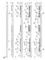
図1は、本発明の回路付サスペンション基板の一実施形態の平面図を、図2は、図1に示す回路付サスペンション基板のジンバル部の平面図、図3は、図1に示す回路付サスペンション基板のジンバル部の底面図、図4は、図2および図3に示すジンバル部のA−A線に沿う断面図、図5は、図2に示すジンバル部の平面図であり、第1ベース絶縁層を明示した平面図、図6は、図3に示すジンバル部の底面図であり、第2ベース絶縁層を明示した底面図、図7〜図9は、回路付サスペンション基板の製造方法を説明するための工程図、図10は、図2に示すジンバル部のステージを揺動させた状態の平面図を示す。 1 is a plan view of an embodiment of a suspension board with circuit of the present invention, FIG. 2 is a plan view of a gimbal portion of the suspension board with circuit shown in FIG. 1, and FIG. 3 is a suspension with circuit shown in FIG. 4 is a bottom view of the gimbal portion of the substrate, FIG. 4 is a cross-sectional view taken along line AA of the gimbal portion shown in FIGS. 2 and 3, and FIG. 5 is a plan view of the gimbal portion shown in FIG. FIG. 6 is a bottom view of the gimbal portion shown in FIG. 3, a bottom view clearly showing the second base insulating layer, and FIGS. 7 to 9 show a method of manufacturing a suspension board with circuit. FIG. 10 is a process diagram for explanation, and FIG. 10 is a plan view showing a state where the stage of the gimbal portion shown in FIG. 2 is swung.
なお、図1、図2および図10において、後述する第1ベース絶縁層21および第1カバー絶縁層23は、後述する第1導体パターン22の相対配置を明確に示すために省略している。
In FIG. 1, FIG. 2, and FIG. 10, the first
また、図3において、後述する第2ベース絶縁層41および第2カバー絶縁層43は、後述する第2導体パターン42の相対配置を明確に示すために、省略している。
In FIG. 3, the second
さらに、図5において、後述する第1カバー絶縁層23は、後述する第1導体パターン22および第1ベース絶縁層21の相対配置を明確に示すために、省略している。
Further, in FIG. 5, the first
さらにまた、図3において、後述する第2カバー絶縁層43は、後述する第2導体パターン42および第2ベース絶縁層41の相対配置を明確に示すために、省略している。
Furthermore, in FIG. 3, the second
図1および図4において、この回路付サスペンション基板1は、磁気ヘッド2を搭載するスライダ3および電子素子としてのピエゾ素子26が搭載されて、ハードディスクドライブ(図示せず)に搭載される。
1 and 4, the suspension board with
回路付サスペンション基板1は、図1に示すように、長手方向に延びる平帯形状に形成されており、長手方向一方側(以下、後側という。)に配置される本体部4と、本体部4の長手方向他方側(以下、先側という。)に配置されるジンバル部5とを一体的に備えている。
As shown in FIG. 1, the suspension board with
本体部4は、長手方向に延びる平面視略矩形状に形成されている。本体部4は、回路付サスペンション基板1がハードディスクドライブに搭載されるときに、ハードディスクドライブのロードビーム(図示せず)に支持されながら、リード・ライト基板などの外部回路基板6(仮想線)、および、電源7(仮想線)に電気的に接続される。
The main body 4 is formed in a substantially rectangular shape in plan view extending in the longitudinal direction. When the suspension board with
ジンバル部5は、本体部4の先端から先側に延びるように形成されている。また、ジンバル部5には、厚み方向(つまり、表裏方向、以下、単に厚み方向という。)を貫通する平面視略矩形状の基板開口部8が形成されている。
The
ジンバル部5は、基板開口部8の幅方向(先後方向に直交する方向)外側に仕切られるアウトリガー部9と、アウトリガー部9に連結されるタング部10とを備えている。
The
アウトリガー部9は、本体部4の幅方向両端部から先側に向かって直線状に延びるように形成されている。
The
図2に示すように、タング部10は、アウトリガー部9の幅方向内側に設けられ、アウトリガー部9の先端部から幅方向内側斜め後方に向かって延びる第1連結部16を介して、アウトリガー部9に連結されている。
As shown in FIG. 2, the
タング部10は、幅方向両側に向かって開く平面視略H字状に形成されている。すなわち、タング部10は、先後方向中央部の幅方向両端部が切り欠かれ(開口され)ている。
The
具体的には、タング部10は、幅方向に長く延びる平面視略矩形状の基部11と、基部11の先側に間隔を隔てて配置され、幅方向に長く延びる平面視略矩形状のステージ12と、基部11およびステージ12の幅方向中央部を連結し、先後方向に長い平面視略矩形状の中央部13とを一体的に備えている。
Specifically, the
タング部10において、切り欠かれた部分には、連通空間14が仕切られている。
In the
連通空間14は、中央部13の幅方向両側に仕切られており、各連通空間14は、回路付サスペンション基板1の厚み方向を貫通するように形成されている。
The
ステージ12には、先後方向中央部分に配線折返部25が区画されている。
In the
配線折返部25は、後述する第1導体パターン22が折り返される領域として、幅方向に長い平面視略矩形状に仕切られている。
The wiring folded
また、ステージ12は、第2連結部17によって、アウトリガー部9に接続されている。
The
第2連結部17は、各アウトリガー部9の先端と、ステージ12の幅方向両端とを湾曲状に連結する湾曲部18と、各アウトリガー部9の先端およびステージ12の先端の幅方向中央を連結するE字部19とを備えている。
The second connecting
湾曲部18は、アウトリガー部9の先端から幅方向内方斜め先側に向かって湾曲状に延び、ステージ12の幅方向両端に至っている。
The
E字部19は、平面視略E字状をなし、具体的には、両アウトリガー部9の先端から先側に向かって延び、その後、幅方向内側に屈曲し、幅方向内側に延びて合一となった後、後側に屈曲して、ステージ12の先端の幅方向中央に至っている。
The
中央部13は、幅方向に湾曲可能な幅狭に形成されている。
The
また、タング部10には、スライダ3を支持するための台座60が設けられている。
The
台座60は、基部11に設けられる第1台座61と、中央部13に設けられる第2台座62とを備えている。
The
第1台座61は、基部11の先側部分に配置され、具体的には、厚み方向に投影したときに、後述する第1導体パターン22と重ならないように、配置されている。第1台座61は、幅方向に互いに間隔を隔てて複数(2つ)設けられている。各第1台座61は、幅方向に長い平面視略矩形状に形成されている。
The
第2台座62は、平面視略円形状をなし、第1台座61の先側に間隔を隔てて設けられ、具体的には、中央部13の先後方向中央部分に配置されている。なお、第2台座62は、厚み方向において、中央部13における第1導体パターン22と重複するように、配置されている。
The
そして、回路付サスペンション基板1は、図4に示すように、金属支持基板20と、金属支持基板20の表面に積層される第1絶縁層としての第1ベース絶縁層21と、第1ベース絶縁層21の表面に積層される第1導体パターン22と、第1ベース絶縁層21の表面に、第1導体パターン22を被覆するように積層される第1カバー絶縁層23とを備えている。
As shown in FIG. 4, the suspension board with
図1に示すように、金属支持基板20は、長手方向に延び、上記した回路付サスペンション基板1の外形形状と実質的に同じ外形形状に形成されている。
As shown in FIG. 1, the
また、図4に示すように、金属支持基板20には、導通開口部29が形成されている。
Further, as shown in FIG. 4, a
導通開口部29は、基部11およびステージ12に、図2が参照されるように、間隔を隔てて複数(4つ)設けられている。具体的には、導通開口部29は、基部11の幅方向両端部およびステージ12の幅方向両端部にそれぞれ形成されている。各導通開口部29は、金属支持基板20を厚み方向に貫通する平面視略円形状に形成されている。
A plurality (four) of
第1ベース絶縁層21は、図4および図5に示すように、第1導体パターン22が形成される部分に対応するように形成されている。
As shown in FIGS. 4 and 5, the first insulating
詳しくは、第1ベース絶縁層21は、本体部4およびジンバル部5の表面全面に形成されるとともに、連通空間14の先端部を被覆するように形成されている。
Specifically, the first insulating
つまり、ステージ12に対応する第1ベース絶縁層21は、その後端縁35が、厚み方向に投影したときに、連通空間14の先端縁よりも後側へ突出している。
That is, the first
なお、基部11に対応する第1ベース絶縁層21は、その先端縁33が、厚み方向に投影したときに、連通空間14の後端縁よりも後側に配置されている。
Note that the first
さらに、第1ベース絶縁層21は、第2連結部17を形成する。
Further, the first
さらにまた、第1ベース絶縁層21は、図4に示すように、金属支持基板20の各導通開口部29の周端縁を円環状に被覆している。これにより、第1ベース絶縁層21には、各導通開口部29に対応する複数(4つ)の第1ベース貫通孔34が、導通開口部29と中心を共有する平面視略円形状に形成されている。
Furthermore, as shown in FIG. 4, the first insulating
第1導体パターン22は、図1および図5に示すように、磁気ヘッド2(図4)に電気的に接続されるヘッド側パターン27と、ピエゾ素子26(図4)に電気的に接続される素子側パターン28とを備えている。
As shown in FIGS. 1 and 5, the
ヘッド側パターン27は、第1端子としてのヘッド側端子30と、外部側端子31と、これらヘッド側端子30および外部側端子31を接続するための信号配線32とを一体的に備えている。
The
ヘッド側端子30は、図2および図5に示すように、ステージ12の幅方向両端部の後端部に複数(4つ)配置されている。具体的には、各ヘッド側端子30は、平面視略矩形状をなし、配線折返部25の後側に配置され、幅方向に互いに間隔を隔てて整列配置されている。また、ヘッド側端子30は、先後方向に投影したときに、中央部13の両側に間隔を隔てて配置されている。
As shown in FIGS. 2 and 5, a plurality (four) of head-
ヘッド側端子30の後端縁57は、図4および図5に示すように、ステージ12における第1ベース絶縁層21の後端縁35よりも先側に退避するように、配置されている。
As shown in FIGS. 4 and 5, the
外部側端子31は、図1に示すように、本体部4の後端部において、幅方向に互いに間隔を隔てて整列配置され、ヘッド側端子30に対応するように、複数(4つ)設けられている。外部側端子31には、仮想線で示す外部回路基板6が接続される。
As shown in FIG. 1, a plurality of (four)
各信号配線32は、対応するヘッド側端子30と外部側端子31とを接続するように、互いに間隔を隔てて、複数(4つ)形成されている。
A plurality (four) of
具体的には、信号配線32の後端は、外部側端子31に連続している。詳しくは、信号配線32は、本体部4の後端部において、外部側端子31から先側に向かって延び、本体部4の先後方向途中において、幅方向両側に向かって2束に分岐状に屈曲する。その後、信号配線32は、本体部4の先後方向途中において、幅方向両端部において先側に屈曲し、本体部4の先端部に向けて、幅方向外端縁に沿って延び、ジンバル部5において、図2および図5に示すように、基板開口部8を通過した後、第1連結部16に至る。
Specifically, the rear end of the
その後、信号配線32は、第1連結部16に沿って後方斜め幅方向内側に延び、基部11の幅方向両端部に至り、幅方向内側に屈曲した後、基部11の幅方向中央において合一する。その後、信号配線32は、中央部13に沿って先側に向かって延び、ステージ12の配線折返部25において、幅方向両側に向かって2束に分岐状に屈曲し、その後、ステージ12の後端縁に沿って幅方向両外側に向かって延び、次いで、後側に折り返された後、ヘッド側端子30の先端部に接続されている。
Thereafter, the
なお、信号配線32は、基部11において、第1台座61の後側に間隔を隔てて配置されている。
In addition, the
素子側パターン28は、図1、図2および図4に示すように、供給側端子36と、表側導通部37と、供給側端子36および表側導通部37を接続するための表側電源配線38とを一体的に備えている。
1, 2, and 4, the element-
供給側端子36は、図1に示すように、本体部4の後端部において、ヘッド側端子30の先側に間隔を隔てて複数(4つ)設けられている。各供給側端子36は、平面視略矩形状をなし、幅方向に間隔を隔てて整列配置されている。供給側端子36には、仮想線で示す電源7が接続される。
As shown in FIG. 1, a plurality (four) of supply-
表側導通部37は、図4に示すように、各第1ベース貫通孔34内にそれぞれ充填されるように、複数(4つ)形成されている。
As shown in FIG. 4, a plurality of (four) front side
表側電源配線38は、図1および図2に示すように、表側導通部37と供給側端子36とに接続されるように、互いに間隔を隔てて、複数(4つ)形成されている。また、表側電源配線38は、本体部4およびジンバル部5にわたって、信号配線32の外側に間隔を隔てて配置されている。
As shown in FIGS. 1 and 2, a plurality of (four) front-side power wirings 38 are formed at intervals from each other so as to be connected to the front-
第1カバー絶縁層23は、図4に示すように、第1導体パターン22が形成される部分に対応して形成されている。
As shown in FIG. 4, the first insulating
具体的には、第1カバー絶縁層23は、ヘッド側パターン27に対応して、外部側端子31(図1参照)およびヘッド側端子30を露出し、信号配線32を被覆するパターンで形成されている。また、第1カバー絶縁層23は、素子側パターン28に対応して、供給側端子36(図1参照)を露出し、表側電源配線38および表側導通部37を被覆するパターンで形成されている。
Specifically, the first
また、上記した第1ベース絶縁層21、第1導体パターン22および第1カバー絶縁層23は、表側支持層63(後述)とともに、各台座60を形成する。
The first
つまり、台座60は、図2および図4に示すように、第1ベース絶縁層21と、その上に順次積層される第1導体パターン22、第1カバー絶縁層23および表側支持層63とを備えている。
That is, as shown in FIGS. 2 and 4, the
各台座60において、第1カバー絶縁層23は、第1導体パターン22を被覆するように形成されている。また、台座60において、表側支持層63は、第1カバー絶縁層23より小さく形成されている。
In each base 60, the first
また、図4に示すように、回路付サスペンション基板1は、金属支持基板20の裏面に積層される第2絶縁層としての第2ベース絶縁層41と、第2ベース絶縁層41の裏面に積層される第2導体パターン42と、第2ベース絶縁層41の裏面に、第2導体パターン42を被覆するように積層される第2カバー絶縁層43とを備えている。
Further, as shown in FIG. 4, the suspension board with
第2ベース絶縁層41は、図4および図6に示すように、次に詳述する第2導体パターン42が形成される部分に対応して形成されている。
As shown in FIGS. 4 and 6, the second insulating
詳しくは、第2ベース絶縁層41は、ジンバル部5の基部11およびステージ12から連通空間14内に臨むように形成されている。具体的には、第2ベース絶縁層41は、4つの導通開口部29に対応して4つ設けられている。各第2ベース絶縁層41は、先後方向および幅方向に互いに間隔を隔てて独立して配置されており、具体的には、基部11およびステージ12の幅方向両端部に配置されている。
Specifically, the second insulating
また、各第2ベース絶縁層41は、底面視において、各導通開口部29を含むように、先後方向に長く延びる略矩形状に形成されている。
In addition, each second
基部11に対応する第2ベース絶縁層41は、基部11の幅方向両端部および連通空間14の後端部にわたって形成されている。
The second
また、基部11に対応する第2ベース絶縁層41の先端縁39は、ジンバル部5において、厚み方向に投影したときに、連通空間14の後端縁よりも先側へ(つまり、連通空間14の先後方向中央に向かって)突出している。すなわち、基部11に対応する第2ベース絶縁層41は、厚み方向に投影したときに、幅方向に沿う金属支持基板20の先端縁54を、先後方向に横切るように形成されている。
Further, the
ステージ12に対応する第2ベース絶縁層41は、ステージ12の幅方向両端部および連通空間14の先端部にわたって形成されている。また、ステージ12に対応する第2ベース絶縁層41は、その後端縁40が、厚み方向に投影したときに第1ベース絶縁層21の後端縁35に重なるように、形成されている。
The second
つまり、第2ベース絶縁層41の後端縁40は、ジンバル部5において、厚み方向に投影したときに、連通空間14の先端縁よりも後側へ(つまり、連通空間14の先後方向中央に向かって)突出している。
That is, the
すなわち、ステージ12に対応する第2ベース絶縁層41は、厚み方向に投影したときに、幅方向に沿う金属支持基板20の後端縁55を、先後方向に横切るように形成されている。
That is, the second insulating
なお、第2ベース絶縁層41は、図4において、基部11およびステージ12において、金属支持基板20の各導通開口部29の周端縁を円環状に被覆している。これにより、第2ベース絶縁層41には、各導通開口部29に対応する複数(4つ)の第2ベース貫通孔47が、導通開口部29と中心を共有する平面視略円形状に形成されている。
In FIG. 4, the second insulating
なお、図6に示すように、第2ベース絶縁層41(図5参照)は、第1ベース絶縁層21とともに、第2連結部17を形成している。
As shown in FIG. 6, the second insulating base layer 41 (see FIG. 5) forms the second connecting
第2導体パターン42は、図3において、裏側導通部44、第2端子としての素子側端子45、および、裏側導通部44と素子側端子45とを接続するための裏側電源配線46を一体的に備えている。
In FIG. 3, the
裏側導通部44は、図4において、各第2ベース貫通孔47内にそれぞれ充填されるように、複数(4つ)形成されている。
In FIG. 4, the back-side
これにより、表側導通部37と裏側導通部44とは、第1ベース貫通孔34内および第2ベース貫通孔47内において、直接接触し、電気的に接続されている。
Thereby, the front side conduction | electrical_connection
素子側端子45は、図3において、基部11に対応する第2ベース絶縁層41の先端部と、ステージ12に対応する第2ベース絶縁層41の後端部とに独立して配置されている。また、各素子側端子45は、連通空間14に臨んでおり、各裏側導通部44に対応するように、幅方向および先後方向に互いに間隔を隔てて複数(4つ)設けられている。各素子側端子45は、底面略矩形状をなし、その幅方向両端縁は、厚み方向に投影したときに、第2ベース絶縁層41(図6)のそれらと同一位置に形成されている。
In FIG. 3, the element-
また、素子側端子45は、連通空間14の後端部に設けられる素子側後端子50と、素子側後端子50の先側に間隔を隔てて設けられる素子側先端子51とを備えている。
The element-
素子側後端子50は、基部11において、幅方向に互いに間隔を隔てて複数(2つ)並列配置されている。
A plurality (two) of element-side
素子側先端子51は、ステージ12において、幅方向に互いに間隔を隔てて複数(2つ)並列配置されている。各素子側先端子51は、図2に示すように、幅方向最外側のヘッド側端子30に対応して設けられており、具体的には、厚み方向に投影したときに、幅方向最外側のヘッド側端子30の後側部分と重複するように、配置されている。
A plurality (two) of element side
幅方向一方側の素子側後端子50および幅方向一方側の素子側先端子51は、中央部13の幅方向一方側の連通空間14を隔てて対をなして設けられている。また、幅方向他方側の素子側後端子50および幅方向他方側の素子側先端子51は、中央部13の幅方向他方側の連通空間14を隔てて対をなして設けられている。
The element-side
素子側後端子50の先端縁48は、図4に示すように、厚み方向に投影したときに、基部11に対応する第2ベース絶縁層41の先端縁39と略面一になるように、配置されている。
As shown in FIG. 4, the leading
素子側先端子51の後端縁49は、厚み方向に投影したときに、ステージ12に対応する第2ベース絶縁層41の後端縁40と略面一になるように、配置されている。
The
また、素子側先端子51の後端縁49は、ヘッド側端子30の後端縁57の後側に微小な間隔を隔てて近接配置されている。
Further, the
裏側電源配線46は、図4および図6に示すように、対応する裏側導通部44と素子側端子45とを接続するように、互いに間隔を隔てて複数(4つ)形成されている。
As shown in FIGS. 4 and 6, a plurality of (four) back side
第2カバー絶縁層43は、図4に示すように、ジンバル部5において、第2導体パターン42に対応するように形成されている。具体的には、第2カバー絶縁層43は、素子側端子45を露出し、裏側電源配線46および裏側導通部44を被覆するように形成されている。
As shown in FIG. 4, the second
そして、この回路付サスペンション基板1には、図2および図4に示すように、スライダ3(図2では仮想線)とピエゾ素子26とが実装される。
Then, as shown in FIGS. 2 and 4, the slider 3 (the phantom line in FIG. 2) and the
スライダ3は、回路付サスペンション基板1とともに、ハードディスクドライブ(図示せず)のロードビーム(図示せず)の先端に実装され、ハードディスクドライブ(図示せず)が駆動されたときには、磁気ディスク(図示せず)に対して、相対的に走行しながら、微小間隔を隔てて浮上される。
The
スライダ3は、平面視略矩形状、かつ、側断面視略矩形状をなし、図2の仮想線で示すように、厚み方向に投影したときに、その先端部が、ステージ12の後端部と重なり、かつ、その後端部が基部11の先端部と重なるように、配置されている。具体的には、スライダ3は、その中央部および後端部が、厚み方向に投影したときに、台座60を含むように、配置されている。
The
また、図4に示すように、スライダ3の先端部には、磁気ヘッド2が、スライダ3の厚み方向全体にわたって搭載されている。磁気ヘッド2は、ヘッド側端子30とはんだボール53によって先後方向に接続される。
As shown in FIG. 4, the
これにより、スライダ3は、その先端部が、ステージ12に固定されるとともに、後端部が、基部11に対して面方向(厚み方向に直交する方向)にスライド可能に支持されている。
As a result, the
また、スライダ3の後端部は、厚み方向に投影したときに、素子側後端子50を含んでいる。
The rear end portion of the
ピエゾ素子26は、図2および図3に示すように、先後方向に伸縮可能であって、先後方向に長い平面視略矩形状に形成されている。また、図4に示すように、ピエゾ素子26は、スライダ3の下側に間隔を隔てて配置されている。
2 and 3, the
詳しくは、図2および図3に示すように、ピエゾ素子26は、連通空間14を先後方向に挟む2組の1対の素子側端子45(素子側先端子51および素子側後端子50)間に架設されるように、搭載されている。
Specifically, as shown in FIGS. 2 and 3, the
より具体的には、図4に示すように、各ピエゾ素子26の先端部の端子が、素子側先端子51の裏面に接合され、それらは、はんだボール53を介して電気的に接続されている。また、各ピエゾ素子26の後端部の端子が、素子側後端子50の裏面に接合され、それらが、はんだボール53を介して電気的に接続されている。
More specifically, as shown in FIG. 4, the terminal at the tip of each
これにより、各ピエゾ素子26は、素子側先端子51および素子側後端子50にそれぞれ固定される。
Thereby, each
また、ピエゾ素子26は、厚み方向に投影したときに、スライダ3と重複しており、具体的には、ピエゾ素子26は、厚み方向に投影したときに、スライダ3にすべて含まれる。
The
また、ピエゾ素子26は、磁気ヘッド2と近接配置されている。
The
そして、ピエゾ素子26は、電源7(図1の仮想線)から素子側パターン28および第2導体パターン42を介して電気が供給され、その電圧が制御されることによって、伸縮する。
The
次に、この回路付サスペンション基板1の製造方法について、図7〜図9を参照して説明する。
Next, a method for manufacturing the suspension board with
この方法では、まず、図7(a)に示すように、金属支持基板20を用意する。
In this method, first, a
金属支持基板20を形成する材料としては、例えば、ステンレス、42アロイ、アルミニウム、銅−ベリリウム、りん青銅などの金属材料が挙げられ、好ましくは、ステンレスが挙げられる。
Examples of the material for forming the
金属支持基板20の厚みは、例えば、15〜50μm、好ましくは、15〜30μmである。
The thickness of the metal support board |
次いで、図7(b)に示すように、金属支持基板20の表面に、感光性の絶縁材料のワニスを塗布して乾燥させた後、露光および現像して、加熱硬化することにより第1ベース絶縁層21を、上記したパターンで形成する。同時に、台座60(図7(d)参照)に対応する第1ベース絶縁層21を形成する。
Next, as shown in FIG. 7B, a photosensitive insulating material varnish is applied to the surface of the
第1ベース絶縁層21を形成する材料としては、例えば、ポリイミド樹脂、ポリアミドイミド樹脂、アクリル樹脂、ポリエーテルニトリル樹脂、ポリエーテルスルホン樹脂、ポリエチレンテレフタレート樹脂、ポリエチレンナフタレート樹脂、ポリ塩化ビニル樹脂などの合成樹脂などの絶縁材料が挙げられる。好ましくは、ポリイミド樹脂が挙げられる。
Examples of the material for forming the first
第1ベース絶縁層21の厚みは、例えば、1〜35μm、好ましくは、3〜15μmである。
The thickness of the 1st
各第1ベース貫通孔34の直径は、例えば、20〜280μm、好ましくは、40〜200μmである。
The diameter of each first base through
次いで、図7(c)に示すように、第1ベース絶縁層21の表面に、第1導体パターン22を、アディティブ法またはサブトラクティブ法などにより形成する。同時に、台座60(図7(d)参照)に対応する第1導体パターン22を、第1ベース絶縁層21の上に形成する。
Next, as shown in FIG. 7C, a
第1導体パターン22を形成する材料は、例えば、銅、ニッケル、金、はんだ、またはそれらの合金などの導体材料などが挙げられ、好ましくは、銅が挙げられる。
Examples of the material forming the
第1導体パターン22の厚みは、例えば、3〜50μm、好ましくは、5〜20μmである。
The thickness of the
各信号配線32および表側電源配線38の幅は、例えば、5〜200μm、好ましくは、8〜100μmである。
The width of each
また、各信号配線32間の間隔(幅方向における間隔、以下同様。)は、例えば、5〜1000μm、好ましくは、8〜100μmである。また、信号配線32と表側電源配線38との間の間隔は、例えば、5〜1000μm、好ましくは、8〜100μmである。
Moreover, the space | interval (space | interval in the width direction, the same hereafter) between each
また、各ヘッド側端子30、各外部側端子31(図1参照)および各供給側端子36(図1参照)の幅は、例えば、15〜1000μm、好ましくは、20〜800μmである。
Moreover, the width of each
また、各ヘッド側端子30間の間隔と、各外部側端子31(図1参照)間の間隔とは、例えば、15〜1000μm、好ましくは、20〜800μmである。
Moreover, the space | interval between each
次いで、図7(d)に示すように、第1ベース絶縁層21の表面に、第1導体パターン22を被覆するように、感光性の絶縁材料のワニスを塗布して乾燥させた後、露光および現像して、加熱硬化することにより第1カバー絶縁層23を上記したパターンで形成する。同時に、台座60に対応する第1カバー絶縁層23を、第1ベース絶縁層21の上に、第1導体パターン22を被覆するように、形成する。
Next, as shown in FIG. 7D, the surface of the first insulating
第1カバー絶縁層23を形成する材料としては、上記した第1ベース絶縁層21の絶縁材料と同様の絶縁材料が挙げられる。第1カバー絶縁層23の厚みは、例えば、1〜40μm、好ましくは、1〜10μmである。
As a material for forming the first insulating
続いて、図7(d)に示すように、台座60に対応する第1カバー絶縁層23の上に、表側支持層63を積層する。表側支持層63は、例えば、上記した絶縁材料または金属材料などから公知の積層方法によって形成する。
Subsequently, as shown in FIG. 7D, the
次いで、図7(e)に示すように、金属支持基板20に、各導通開口部29を形成する。
Next, as shown in FIG. 7E, each
各導通開口部29は、例えば、ドライエッチング(例えば、プラズマエッチング)やウェットエッチング(例えば、化学エッチング)などのエッチング法、例えば、ドリル穿孔、例えば、レーザ加工などにより、形成する。好ましくは、エッチング法により形成する。
Each
これにより、金属支持基板20の導通開口部29から、第1ベース絶縁層21の裏面と、表側導通部37の裏面とを露出させる。
As a result, the back surface of the first insulating
各導通開口部29の内径は、例えば、50〜300μm、好ましくは、100〜250μmである。
The internal diameter of each conduction |
次いで、図8(f)に示すように、金属支持基板20の裏面(各導通開口部29から露出される第1ベース絶縁層21の裏面および表側導通部37の裏面を含む。)に、感光性の絶縁材料のワニスを塗布して乾燥させた後、露光および現像して、加熱硬化することにより第2ベース絶縁層41を、上記したパターンで形成する。
Next, as shown in FIG. 8 (f), the back surface of the metal support substrate 20 (including the back surface of the first
第2ベース絶縁層41を形成する材料としては、上記した第1ベース絶縁層21の絶縁材料と同様の絶縁材料が挙げられる。
Examples of the material for forming the second
第2ベース絶縁層41の厚みは、例えば、1〜35μm、好ましくは、8〜15μmである。
The thickness of the second insulating
各第2ベース貫通孔47の直径は、例えば、20〜280μm、好ましくは、40〜200μmである。
The diameter of each second base through
次いで、図8(g)に示すように、第2ベース絶縁層41の裏面に、第2導体パターン42を、アディティブ法またはサブトラクティブ法などにより形成する。
Next, as shown in FIG. 8G, a
第2導体パターン42を形成する材料としては、第1導体パターン22の導体材料と同様の導体材料が挙げられる。
Examples of the material for forming the
第2導体パターン42の厚みは、例えば、3〜50μm、好ましくは、5〜20μmである。
The thickness of the
各裏側電源配線46の幅は、例えば、5〜200μm、好ましくは、8〜100μmである。
The width of each back side
また、各素子側端子45の幅は、例えば、15〜1000μm、好ましくは、20〜800μmである。
Moreover, the width | variety of each
次いで、図9(h)に示すように、第2ベース絶縁層41の裏面に、裏側の第2導体パターン42を被覆するように、感光性の絶縁材料のワニスを塗布して乾燥させた後、露光および現像して、加熱硬化することにより第2カバー絶縁層43を上記したパターンで形成する。
Next, as shown in FIG. 9 (h), after applying and drying a photosensitive insulating material varnish on the back surface of the second
第2カバー絶縁層43を形成する材料としては、上記した第1ベース絶縁層21の絶縁材料と同様の絶縁材料が挙げられる。第2カバー絶縁層43の厚みは、例えば、1〜40μm、好ましくは、1〜10μmである。
Examples of the material for forming the second
次いで、図9(i)に示すように、金属支持基板20に基板開口部8(図1参照)および連通空間14を形成する。
Next, as shown in FIG. 9I, the substrate opening 8 (see FIG. 1) and the
連通空間14および基板開口部8は、例えば、化学エッチングなどのウェットエッチングにより形成する。
The
このとき、連通空間14を形成するには、エッチング時間を比較的長く設定して、金属支持基板20をオーバーエッチングすることにより、第1ベース絶縁層21と第2ベース絶縁層41との間にあり、ステージ12に対応する金属支持基板20を先側へエッチング(オーバーエッチング)するとともに、第2ベース絶縁層41の表側にあり、基部11に対応する金属支持基板20を後側へエッチング(オーバーエッチング)する。
At this time, in order to form the
これにより、図4に示すように、ステージ12における金属支持基板20の後端縁55が、ステージ12に対応する第1ベース絶縁層21の後端縁35および第2ベース絶縁層41の後端縁49よりも、先側に配置される。
As a result, as shown in FIG. 4, the
すなわち、第1ベース絶縁層21の後端縁35および第2ベース絶縁層41の後端縁49は、金属支持基板20の後端縁55よりも、連通空間14内に突出する。
That is, the
また、基部11に対応する第2ベース絶縁層41の先端縁39が、基部11における金属支持基板20の先端縁54よりも、連通空間14内に突出する。
Further, the leading
次いで、金属支持基板20を外形加工して、回路付サスペンション基板1を得る。
Next, the
その後、回路付サスペンション基板1の表面側において、磁気ヘッド2が設けられたスライダ3を、台座60の上面に載置する。これにより、スライダ3は、台座60に面方向にスライド可能に支持される。
Thereafter, the
続いて、ヘッド側端子30の表面に、はんだボール53を、はんだボール53が磁気ヘッド2の端子(側面端子)に接触するように、設ける。
Subsequently, the
これとともに、回路付サスペンション基板1の裏面側において、ピエゾ素子26の先端部および後端部を、素子側先端子51および素子側後端子50に接合する。つまり、ヘッド側端子30の表面、および、素子側端子45の裏面に、はんだボール53をそれぞれ設ける。
At the same time, the front end portion and the rear end portion of the
これにより、各ピエゾ素子26は、1対の素子側端子45(素子側先端子51および素子側後端子50)間に架設されるように、回路付サスペンション基板1に搭載される。
Thus, each
そして、各はんだボール53を溶融させることにより、ヘッド側端子30を磁気ヘッド2に固定して電気的に接続する。
Then, by melting each
同時に、素子側端子45をピエゾ素子26に固定して電気的に接続させる。
At the same time, the
なお、図1が参照されるように、外部側端子31を外部回路基板6と電気的に接続させるとともに、供給側端子36を電源7と電気的に接続させる。
As shown in FIG. 1, the
これにより、回路付サスペンション基板1にスライダ3およびピエゾ素子26が搭載される。
As a result, the
次に、ピエゾ素子26の伸縮によるスライダ3の揺動について、図10を参照して説明する。
Next, swinging of the
まず、ピエゾ素子26は、電気が電源7(図1)から素子側端子45を介して供給され、電気の電圧が制御されることによって、一方が収縮する。すると、一方のピエゾ素子26を固定する素子側先端子51および素子側後端子50が相対的に近接する。つまり、ステージ12に支持される一方の素子側先端子51が、基部11に支持される一方の素子側後端子50に対して後側に移動する。
First, electricity is supplied to the
これと同時に、電気が電源7(図1)から素子側端子45を介して供給され、電気の電圧が制御されることによって、他方のピエゾ素子26が伸長する。すると、他方のピエゾ素子26を固定する素子側先端子51および素子側後端子50が相対的に離間する。つまり、ステージ12に支持される他方の素子側先端子51が、基部11に支持される他方の素子側後端子50に対して、先側に移動する。
At the same time, electricity is supplied from the power source 7 (FIG. 1) via the element-
これにより、中央部13の先端および先後方向途中が、幅方向一方側に湾曲しながら、ステージ12が、中央部13の後端を支点として、幅方向一方側に向かって揺動する。これとともに、スライダ3の先側部分が幅方向一方側に向かって揺動する。
As a result, the
一方、図示しないが、一方のピエゾ素子26を伸長させ、他方のピエゾ素子26を収縮させれば、スライダ3の先側部分が上記と逆向き(幅方向他方側)に揺動する。
On the other hand, although not shown, when one
そして、この回路付サスペンション基板1によれば、ジンバル部5を厚み方向に投影したときに、第1ベース絶縁層21の後端縁35および第2ベース絶縁層41の後端縁40は、金属支持基板20の後端縁55よりも連通空間14内に突出している。
According to the suspension board with
すなわち、金属支持基板20の後端縁55は、第1ベース絶縁層21の後端縁35および第2ベース絶縁層41の後端縁40に対して、先側へ退避されている。
That is, the
また、ジンバル部5を厚み方向に投影したときに、第2ベース絶縁層41の先端縁39は、金属支持基板20の先端縁54よりも連通空間14内に突出している。
Further, when the
すなわち、金属支持基板20の先端縁54は、第2ベース絶縁層41の先端縁39に対して、後側へ退避されている。
That is, the leading
そのため、素子側先端子51および素子側後端子50と、ピエゾ素子26とをはんだボール53で接続するときに、溶融したはんだが金属支持基板20に向かって流れたとしても、はんだが金属支持基板20に接触することを防止することができる。
Therefore, when the element-
また、ヘッド側端子30と、スライダ3に搭載される磁気ヘッド2とをはんだボール53で接続するときに、溶融したはんだが金属支持基板20に向かって流れたとしても、はんだが金属支持基板20に接触することを防止することができる。
Further, when the head-
具体的には、図4が参照されるように、スライダ3の先端部の下面と、ヘッド側端子30の上面およびヘッド側端子30より後側の第1ベース絶縁層21の上面との隙間に沿って、溶融したはんだが金属支持基板20に向かって流れたとしても、はんだが金属支持基板20に接触することを防止することができる。
Specifically, as shown in FIG. 4, a gap is formed between the lower surface of the tip of the
あるいは、上記した隙間が形成されない場合でも、ヘッド側端子30の上面および第1ベース絶縁層21の上面において、溶融したはんだが、スライダ3(磁気ヘッド2)の先端面に沿って、幅方向外側に流れ、その後、スライダ3の幅方向側端面に回り込んだ後、金属支持基板20に向かって流れたとしても、はんだが金属支持基板20に接触することを防止することができる。
Alternatively, even when the above-described gap is not formed, the melted solder on the upper surface of the head-
その結果、素子側端子45と金属支持基板20との短絡、および、ヘッド側端子30と金属支持基板20との短絡を防止することができる。
As a result, a short circuit between the
しかも、ピエゾ素子26は、スライダ3と重複しているので、基部11およびステージ12の相対的な離間または近接に対して、スライダ3を精度よく揺動させることができる。
(変形例)
図12および図13は、本発明の回路付サスペンション基板の変形例を説明する説明図である。なお、図12および図13において、上記した実施形態と同様の部材については、同一の参照符号を付し、その詳細な説明を省略する。
In addition, since the
(Modification)
12 and 13 are explanatory views for explaining a modification of the suspension board with circuit of the present invention. 12 and 13, members similar to those in the above-described embodiment are given the same reference numerals, and detailed descriptions thereof are omitted.
上記した実施形態において、素子側後端子50に積層される第2ベース絶縁層41の先端縁39、素子側先端子51に積層される第2ベース絶縁層41の後端縁40、および、ヘッド側端子30に積層される第1ベース絶縁層21の後端縁35が、連通空間14内に突出するように形成されていれば、素子側後端子50、素子側先端子51、ヘッド側端子30、第1ベース絶縁層21および第2ベース絶縁層41の形状は、特に限定されない。
In the above-described embodiment, the
例えば、第1の変形例では、図12(a)に示すように、素子側後端子50は、素子側後端子50に積層される第2ベース絶縁層41の先端縁39よりも先側へ突出するように形成することもできる。
For example, in the first modified example, as shown in FIG. 12A, the element-side
詳しくは、素子側後端子50は、第2ベース絶縁層41の裏面に形成され、その後端部において上側へ屈曲されて、第2ベース絶縁層41の先端縁39に沿うように上側へ延び、その上端部において先側へ屈曲されて先側へ延びている。なお、素子側後端子50の突出部分(第2ベース絶縁層41よりも先側に配置される部分)の上面は、素子側後端子50に積層される第2ベース絶縁層41の上面と面一となるように形成されている。
Specifically, the element-side
つまり、素子側後端子50において、第2ベース絶縁層41の裏面に形成される部分と、第2ベース絶縁層41よりも先側に配置される部分とに段差LDがある。
That is, in the element-side
段差LDは、適宜調整することができる。 The level difference LD can be adjusted as appropriate.
段差LDを調整するには、例えば、第2ベース絶縁層41を形成する工程(図8(f)参照)において、階調露光などの方法により、第2ベース絶縁層41に、素子側後端子50の突出部分に対応する段差LDを形成し、その後、金属支持基板20をエッチング(図9(i)参照)した後において、素子側後端子50の突出部分の上面を露出させるように、第2ベース絶縁層41をエッチングする。
In order to adjust the level difference LD, for example, in the step of forming the second base insulating layer 41 (see FIG. 8F), the element-side rear terminal is connected to the second
例えば、第2の変形例では、図12(b)に示すように、第2ベース絶縁層41の裏面に形成される部分と、第2ベース絶縁層41よりも先側に配置される部分との段差LDを、第1の変形例の約半分の長さにする。
For example, in the second modification, as shown in FIG. 12B, a portion formed on the back surface of the second insulating
また、素子側先端子51およびヘッド側端子30の少なくとも一方において、上記した第1の変形例で説明した素子側後端子50と同様に、第2ベース絶縁層41の端縁よりも連通空間14内に突出するように形成することができる。
Further, in at least one of the element-
また、素子側先端子51およびヘッド側端子30の少なくとも一方を第2ベース絶縁層41よりも突出させた場合において、上記した第2の変形例と同様に、段差LDを、適宜調整することができる。
Further, when at least one of the element-
具体的には、第3の変形例では、図13(a)に示すように、素子側先端子51を、素子側先端子51に積層される第2ベース絶縁層41の後端縁40よりも後側へ突出するように形成することができる。
Specifically, in the third modification example, as shown in FIG. 13A, the element-
また、第4の変形例では、図13(b)に示すように、素子側先端子51において、第2ベース絶縁層41の裏面に形成される部分と、第2ベース絶縁層41よりも後側に配置される部分との段差LDを、第3の変形例の約半分の長さにする。
Further, in the fourth modification example, as shown in FIG. 13B, in the element-
また、第5の変形例では、図13(c)に示すように、ヘッド側端子30を、ヘッド側端子30に積層される第1ベース絶縁層21の後端縁35よりも後側へ突出するように形成することができる。
Further, in the fifth modified example, as shown in FIG. 13C, the
また、第6の変形例では、図13(d)に示すように、ヘッド側端子30において、第1ベース絶縁層21の表面に形成される部分と、第1ベース絶縁層21よりも後側に配置される部分との段差LDを、第5の変形例の約半分の長さにする。
Further, in the sixth modification, as shown in FIG. 13D, in the
また、第7の変形例では、図13(e)に示すように、素子側先端子51を、素子側先端子51に積層される第2ベース絶縁層41の後端縁40よりも後側へ突出するように形成するとともに、ヘッド側端子30を、ヘッド側端子30に積層される第1ベース絶縁層21の後端縁35よりも後側へ突出するように形成することができる。
Further, in the seventh modified example, as shown in FIG. 13E, the element-
また、第8の変形例では、図13(f)に示すように、素子側先端子51において、第2ベース絶縁層41の裏面に形成される部分と、第2ベース絶縁層41よりも後側に配置される部分との段差LDを、第7の変形例の約半分の長さにするとともに、ヘッド側端子30において、第1ベース絶縁層21の表面に形成される部分と、第1ベース絶縁層21よりも後側に配置される部分との段差LDを、第7の変形例の約半分の長さにする。
Further, in the eighth modification, as shown in FIG. 13F, in the element-
なお、上記した各変形例は、互いに組み合わせることができる。 Note that the above-described modifications can be combined with each other.
1 回路付サスペンション基板
2 磁気ヘッド
3 スライダ
14 連通空間
20 金属支持基板
21 第1ベース絶縁層
22 第1導体パターン
26 ピエゾ素子
30 ヘッド側端子
33 先端縁(第1ベース絶縁層)
35 後端縁(第1ベース絶縁層)
39 先端縁(第2ベース絶縁層)
40 後端縁(第2ベース絶縁層)
41 第2ベース絶縁層
42 第2導体パターン
45 素子側端子
54 先端縁(金属支持基板)
55 後端縁(金属支持基板)
DESCRIPTION OF
35 Rear edge (first base insulating layer)
39 Tip edge (second base insulating layer)
40 Rear edge (second base insulating layer)
41 Second
55 Rear edge (metal support board)
Claims (3)
金属支持基板と、
前記金属支持基板の表面に積層される第1絶縁層と、
前記第1絶縁層の前記表面側に積層される第1端子を備える第1導体パターンと、
前記金属支持基板の裏面に積層される第2絶縁層と、
前記第2絶縁層の前記裏面側に積層される第2端子を備える第2導体パターンと
を備え、
前記回路付サスペンション基板には、表裏方向に連通する連通空間が形成され、
前記第1端子は、前記スライダの前記磁気ヘッドが電気的に接続されるように構成され、
前記第2端子は、前記電子素子が電気的に接続されるように構成され、前記電子素子が架設されるように前記連通空間を隔てて少なくとも1対設けられ、
前記表裏方向に投影したときに、前記第1絶縁層および前記第2絶縁層の端縁は、前記金属支持基板の端縁よりも前記連通空間内に突出している
ことを特徴とする、回路付サスペンション基板。 A suspension board with circuit configured to be able to mount an external slider for mounting a magnetic head and an external electronic element provided in the vicinity of the magnetic head,
A metal support substrate;
A first insulating layer laminated on a surface of the metal support substrate;
A first conductor pattern comprising a first terminal laminated on the surface side of the first insulating layer;
A second insulating layer laminated on the back surface of the metal support substrate;
A second conductor pattern comprising a second terminal laminated on the back side of the second insulating layer,
The suspension board with circuit is formed with a communication space communicating in the front and back direction,
The first terminal is configured to be electrically connected to the magnetic head of the slider,
The second terminals are configured such that the electronic elements are electrically connected, and at least one pair is provided across the communication space so that the electronic elements are installed,
When projected in the front-back direction, the edges of the first insulating layer and the second insulating layer protrude into the communication space from the edges of the metal support substrate. Suspension board.
Priority Applications (1)
| Application Number | Priority Date | Filing Date | Title |
|---|---|---|---|
| JP2012151724A JP5896846B2 (en) | 2011-08-22 | 2012-07-05 | Suspension board with circuit |
Applications Claiming Priority (3)
| Application Number | Priority Date | Filing Date | Title |
|---|---|---|---|
| JP2011180972 | 2011-08-22 | ||
| JP2011180972 | 2011-08-22 | ||
| JP2012151724A JP5896846B2 (en) | 2011-08-22 | 2012-07-05 | Suspension board with circuit |
Publications (2)
| Publication Number | Publication Date |
|---|---|
| JP2013062013A JP2013062013A (en) | 2013-04-04 |
| JP5896846B2 true JP5896846B2 (en) | 2016-03-30 |
Family
ID=47534425
Family Applications (1)
| Application Number | Title | Priority Date | Filing Date |
|---|---|---|---|
| JP2012151724A Expired - Fee Related JP5896846B2 (en) | 2011-08-22 | 2012-07-05 | Suspension board with circuit |
Country Status (3)
| Country | Link |
|---|---|
| US (1) | US8508888B2 (en) |
| JP (1) | JP5896846B2 (en) |
| CN (1) | CN102890940B (en) |
Families Citing this family (23)
| Publication number | Priority date | Publication date | Assignee | Title |
|---|---|---|---|---|
| JP5603657B2 (en) | 2010-05-20 | 2014-10-08 | 日東電工株式会社 | Suspension board with circuit and manufacturing method thereof |
| US8885299B1 (en) | 2010-05-24 | 2014-11-11 | Hutchinson Technology Incorporated | Low resistance ground joints for dual stage actuation disk drive suspensions |
| US8861142B2 (en) * | 2010-10-13 | 2014-10-14 | Nitto Denko Corporation | Suspension board with circuit and producing method thereof |
| JP5781773B2 (en) * | 2011-01-12 | 2015-09-24 | 日東電工株式会社 | Suspension board with circuit |
| JP6024078B2 (en) * | 2011-08-17 | 2016-11-09 | 大日本印刷株式会社 | Suspension board |
| JP5974824B2 (en) * | 2012-10-25 | 2016-08-23 | 大日本印刷株式会社 | Suspension substrate, suspension, suspension with head, hard disk drive, and method for manufacturing suspension substrate |
| JP6043613B2 (en) * | 2012-12-11 | 2016-12-14 | 日東電工株式会社 | Suspension board with circuit |
| US8982513B1 (en) * | 2013-05-21 | 2015-03-17 | Western Digital Technologies, Inc. | Disk drive head suspension with dual piezoelectric elements adhered to rotary-actuated and non-actuated portions of a structural layer of a tongue of a laminated flexure |
| US8896969B1 (en) | 2013-05-23 | 2014-11-25 | Hutchinson Technology Incorporated | Two-motor co-located gimbal-based dual stage actuation disk drive suspensions with motor stiffeners |
| JP6169960B2 (en) * | 2013-12-04 | 2017-07-26 | 日東電工株式会社 | Method for manufacturing suspension board with circuit |
| JP6370619B2 (en) * | 2014-06-26 | 2018-08-08 | 日東電工株式会社 | Suspension board with circuit and manufacturing method thereof |
| JP6522317B2 (en) * | 2014-11-10 | 2019-05-29 | 日東電工株式会社 | Printed circuit board and method of manufacturing the same, and printed circuit board assembly and method of manufacturing the same |
| US9070392B1 (en) | 2014-12-16 | 2015-06-30 | Hutchinson Technology Incorporated | Piezoelectric disk drive suspension motors having plated stiffeners |
| US9318136B1 (en) * | 2014-12-22 | 2016-04-19 | Hutchinson Technology Incorporated | Multilayer disk drive motors having out-of-plane bending |
| US9296188B1 (en) | 2015-02-17 | 2016-03-29 | Hutchinson Technology Incorporated | Partial curing of a microactuator mounting adhesive in a disk drive suspension |
| CN107735834B (en) | 2015-06-30 | 2019-11-19 | 哈钦森技术股份有限公司 | Disk drive head suspension structure with improved reliability |
| US9646638B1 (en) | 2016-05-12 | 2017-05-09 | Hutchinson Technology Incorporated | Co-located gimbal-based DSA disk drive suspension with traces routed around slider pad |
| JP6687490B2 (en) * | 2016-09-07 | 2020-04-22 | 日東電工株式会社 | Suspension board with circuit and method of manufacturing suspension board with circuit |
| JP6788442B2 (en) * | 2016-09-07 | 2020-11-25 | 日東電工株式会社 | Manufacturing method of suspension board with circuit and suspension board with circuit |
| JP6979287B2 (en) * | 2017-06-09 | 2021-12-08 | 日東電工株式会社 | Suspension board with circuit |
| JP6865643B2 (en) * | 2017-06-09 | 2021-04-28 | 日東電工株式会社 | Suspension board with circuit |
| US10783909B1 (en) * | 2018-05-14 | 2020-09-22 | Seagate Technology | In-plane gimbal tongue microactuator system |
| JP7413237B2 (en) * | 2020-11-16 | 2024-01-15 | 株式会社東芝 | Suspension assembly and disc device |
Family Cites Families (15)
| Publication number | Priority date | Publication date | Assignee | Title |
|---|---|---|---|---|
| US5896247A (en) * | 1997-05-23 | 1999-04-20 | International Business Machines Corporation | Disk file suspension formed flexure |
| US6262868B1 (en) * | 1997-12-30 | 2001-07-17 | International Business Machines Corporation | Method and structures used for connecting recording head signal wires in a microactuator |
| US6195227B1 (en) * | 1997-12-30 | 2001-02-27 | International Business Machines, Inc. | Integrated 3D limiters for microactuators |
| US7612967B2 (en) * | 2001-12-05 | 2009-11-03 | Samsung Electronics Co., Ltd. | Method and apparatus coupling at least one piezoelectric device to a slider in a hard disk drive for microactuation |
| JP2005251262A (en) * | 2004-03-02 | 2005-09-15 | Hitachi Global Storage Technologies Netherlands Bv | Head/slider support structure, and rotary disk-shaped storage device |
| JP4238195B2 (en) * | 2004-10-25 | 2009-03-11 | 日東電工株式会社 | Suspension board with circuit |
| US7518830B1 (en) * | 2006-04-19 | 2009-04-14 | Hutchinson Technology Incorporated | Dual sided electrical traces for disk drive suspension flexures |
| JP5032949B2 (en) * | 2007-11-14 | 2012-09-26 | エイチジーエスティーネザーランドビーブイ | Microactuator, head gimbal assembly and disk drive device |
| JP5147591B2 (en) * | 2008-08-06 | 2013-02-20 | 日東電工株式会社 | Suspension board with circuit, manufacturing method thereof, and positioning method of suspension board with circuit |
| JP5138549B2 (en) | 2008-10-31 | 2013-02-06 | 日東電工株式会社 | Suspension board with circuit |
| JP5027778B2 (en) * | 2008-10-31 | 2012-09-19 | 日東電工株式会社 | Suspension board with circuit |
| JP5002574B2 (en) * | 2008-11-11 | 2012-08-15 | 日東電工株式会社 | Suspension board with circuit and manufacturing method thereof |
| JP2010123195A (en) * | 2008-11-19 | 2010-06-03 | Hitachi Global Storage Technologies Netherlands Bv | Head gimbal assembly, micro-actuator, and method for manufacturing micro-actuator |
| JP5570111B2 (en) * | 2008-12-18 | 2014-08-13 | エイチジーエスティーネザーランドビーブイ | Head gimbal assembly and disk drive |
| US8854826B2 (en) * | 2010-10-07 | 2014-10-07 | Nitto Denko Corporation | Suspension board with circuit |
-
2012
- 2012-07-05 JP JP2012151724A patent/JP5896846B2/en not_active Expired - Fee Related
- 2012-07-19 US US13/553,107 patent/US8508888B2/en not_active Expired - Fee Related
- 2012-07-20 CN CN201210254776.7A patent/CN102890940B/en not_active Expired - Fee Related
Also Published As
| Publication number | Publication date |
|---|---|
| US20130021699A1 (en) | 2013-01-24 |
| CN102890940B (en) | 2016-12-07 |
| JP2013062013A (en) | 2013-04-04 |
| CN102890940A (en) | 2013-01-23 |
| US8508888B2 (en) | 2013-08-13 |
Similar Documents
| Publication | Publication Date | Title |
|---|---|---|
| JP5896846B2 (en) | Suspension board with circuit | |
| JP6029813B2 (en) | Suspension board with circuit | |
| JP5896845B2 (en) | Printed circuit board | |
| JP5138549B2 (en) | Suspension board with circuit | |
| JP6043613B2 (en) | Suspension board with circuit | |
| US8854826B2 (en) | Suspension board with circuit | |
| JP5989370B2 (en) | Printed circuit board | |
| US8208225B2 (en) | Suspension board with circuit and producing method thereof | |
| US8593823B2 (en) | Suspension board with circuit | |
| US20130014976A1 (en) | Wired circuit board and producing method thereof | |
| JP5801085B2 (en) | Suspension board with circuit | |
| US8810970B2 (en) | Suspension substrate, suspension, and manufacturing method of suspension substrate | |
| JP6392085B2 (en) | Suspension board with circuit | |
| JP5752948B2 (en) | Suspension board with circuit | |
| JP6646425B2 (en) | Suspension board with circuit and method of manufacturing the same | |
| JP2012104211A (en) | Suspension board having circuit and method for manufacturing the same | |
| JP6280828B2 (en) | Suspension board with circuit | |
| JP6539194B2 (en) | Suspension board with circuit and method of manufacturing the same | |
| JP6865643B2 (en) | Suspension board with circuit | |
| JP6818169B2 (en) | Suspension board with circuit | |
| JP5240375B1 (en) | Suspension board, suspension, suspension with element, and hard disk drive |
Legal Events
| Date | Code | Title | Description |
|---|---|---|---|
| A621 | Written request for application examination |
Free format text: JAPANESE INTERMEDIATE CODE: A621 Effective date: 20150424 |
|
| A977 | Report on retrieval |
Free format text: JAPANESE INTERMEDIATE CODE: A971007 Effective date: 20151214 |
|
| TRDD | Decision of grant or rejection written | ||
| A01 | Written decision to grant a patent or to grant a registration (utility model) |
Free format text: JAPANESE INTERMEDIATE CODE: A01 Effective date: 20160209 |
|
| A61 | First payment of annual fees (during grant procedure) |
Free format text: JAPANESE INTERMEDIATE CODE: A61 Effective date: 20160301 |
|
| R150 | Certificate of patent or registration of utility model |
Ref document number: 5896846 Country of ref document: JP Free format text: JAPANESE INTERMEDIATE CODE: R150 |
|
| LAPS | Cancellation because of no payment of annual fees |