JP4305016B2 - Piezoelectric actuator unit and liquid jet head using the same - Google Patents
Piezoelectric actuator unit and liquid jet head using the same Download PDFInfo
- Publication number
- JP4305016B2 JP4305016B2 JP2003070545A JP2003070545A JP4305016B2 JP 4305016 B2 JP4305016 B2 JP 4305016B2 JP 2003070545 A JP2003070545 A JP 2003070545A JP 2003070545 A JP2003070545 A JP 2003070545A JP 4305016 B2 JP4305016 B2 JP 4305016B2
- Authority
- JP
- Japan
- Prior art keywords
- electrode
- piezoelectric
- pressure chamber
- actuator unit
- piezoelectric element
- Prior art date
- Legal status (The legal status is an assumption and is not a legal conclusion. Google has not performed a legal analysis and makes no representation as to the accuracy of the status listed.)
- Expired - Fee Related
Links
- 239000007788 liquid Substances 0.000 title claims description 31
- 239000000758 substrate Substances 0.000 claims abstract description 41
- 239000000463 material Substances 0.000 claims description 34
- 238000004891 communication Methods 0.000 claims description 15
- 238000000034 method Methods 0.000 claims description 13
- 230000008859 change Effects 0.000 claims description 5
- 239000004020 conductor Substances 0.000 claims description 4
- 238000010030 laminating Methods 0.000 claims description 2
- 239000010410 layer Substances 0.000 description 122
- 239000007772 electrode material Substances 0.000 description 15
- 238000004519 manufacturing process Methods 0.000 description 11
- 230000015572 biosynthetic process Effects 0.000 description 9
- 230000005684 electric field Effects 0.000 description 9
- 239000000919 ceramic Substances 0.000 description 8
- 239000002356 single layer Substances 0.000 description 8
- 230000004048 modification Effects 0.000 description 6
- 238000012986 modification Methods 0.000 description 6
- 238000007639 printing Methods 0.000 description 6
- 230000000694 effects Effects 0.000 description 5
- 230000007423 decrease Effects 0.000 description 4
- 230000007547 defect Effects 0.000 description 4
- 238000010304 firing Methods 0.000 description 4
- 239000002243 precursor Substances 0.000 description 4
- 230000008569 process Effects 0.000 description 4
- 238000010586 diagram Methods 0.000 description 3
- 239000000853 adhesive Substances 0.000 description 2
- 230000001070 adhesive effect Effects 0.000 description 2
- 230000008602 contraction Effects 0.000 description 2
- 230000002950 deficient Effects 0.000 description 2
- 229910052451 lead zirconate titanate Inorganic materials 0.000 description 2
- 239000004973 liquid crystal related substance Substances 0.000 description 2
- 229910052751 metal Inorganic materials 0.000 description 2
- 239000002184 metal Substances 0.000 description 2
- 150000002739 metals Chemical class 0.000 description 2
- BASFCYQUMIYNBI-UHFFFAOYSA-N platinum Chemical compound [Pt] BASFCYQUMIYNBI-UHFFFAOYSA-N 0.000 description 2
- 230000004043 responsiveness Effects 0.000 description 2
- 229910003781 PbTiO3 Inorganic materials 0.000 description 1
- 229910020698 PbZrO3 Inorganic materials 0.000 description 1
- BQCADISMDOOEFD-UHFFFAOYSA-N Silver Chemical compound [Ag] BQCADISMDOOEFD-UHFFFAOYSA-N 0.000 description 1
- 229910045601 alloy Inorganic materials 0.000 description 1
- 239000000956 alloy Substances 0.000 description 1
- 230000004075 alteration Effects 0.000 description 1
- PNEYBMLMFCGWSK-UHFFFAOYSA-N aluminium oxide Inorganic materials [O-2].[O-2].[O-2].[Al+3].[Al+3] PNEYBMLMFCGWSK-UHFFFAOYSA-N 0.000 description 1
- 229910002113 barium titanate Inorganic materials 0.000 description 1
- 238000005452 bending Methods 0.000 description 1
- 150000001875 compounds Chemical class 0.000 description 1
- 238000005520 cutting process Methods 0.000 description 1
- 238000010292 electrical insulation Methods 0.000 description 1
- PCHJSUWPFVWCPO-UHFFFAOYSA-N gold Chemical compound [Au] PCHJSUWPFVWCPO-UHFFFAOYSA-N 0.000 description 1
- 239000010931 gold Substances 0.000 description 1
- 229910052737 gold Inorganic materials 0.000 description 1
- HFGPZNIAWCZYJU-UHFFFAOYSA-N lead zirconate titanate Chemical compound [O-2].[O-2].[O-2].[O-2].[O-2].[Ti+4].[Zr+4].[Pb+2] HFGPZNIAWCZYJU-UHFFFAOYSA-N 0.000 description 1
- 239000011159 matrix material Substances 0.000 description 1
- 229910044991 metal oxide Inorganic materials 0.000 description 1
- 150000004706 metal oxides Chemical class 0.000 description 1
- 239000000203 mixture Substances 0.000 description 1
- RVTZCBVAJQQJTK-UHFFFAOYSA-N oxygen(2-);zirconium(4+) Chemical compound [O-2].[O-2].[Zr+4] RVTZCBVAJQQJTK-UHFFFAOYSA-N 0.000 description 1
- 238000005192 partition Methods 0.000 description 1
- 229910052697 platinum Inorganic materials 0.000 description 1
- 230000010287 polarization Effects 0.000 description 1
- 229920000642 polymer Polymers 0.000 description 1
- 229920006254 polymer film Polymers 0.000 description 1
- 239000000843 powder Substances 0.000 description 1
- 238000003825 pressing Methods 0.000 description 1
- 230000002265 prevention Effects 0.000 description 1
- 239000011241 protective layer Substances 0.000 description 1
- 238000004080 punching Methods 0.000 description 1
- 230000004044 response Effects 0.000 description 1
- 238000007789 sealing Methods 0.000 description 1
- 229910052709 silver Inorganic materials 0.000 description 1
- 239000004332 silver Substances 0.000 description 1
- 239000011800 void material Substances 0.000 description 1
- 229910001928 zirconium oxide Inorganic materials 0.000 description 1
Images


Classifications
-
- B—PERFORMING OPERATIONS; TRANSPORTING
- B41—PRINTING; LINING MACHINES; TYPEWRITERS; STAMPS
- B41J—TYPEWRITERS; SELECTIVE PRINTING MECHANISMS, i.e. MECHANISMS PRINTING OTHERWISE THAN FROM A FORME; CORRECTION OF TYPOGRAPHICAL ERRORS
- B41J2/00—Typewriters or selective printing mechanisms characterised by the printing or marking process for which they are designed
- B41J2/005—Typewriters or selective printing mechanisms characterised by the printing or marking process for which they are designed characterised by bringing liquid or particles selectively into contact with a printing material
- B41J2/01—Ink jet
- B41J2/135—Nozzles
- B41J2/14—Structure thereof only for on-demand ink jet heads
- B41J2/14201—Structure of print heads with piezoelectric elements
- B41J2/14233—Structure of print heads with piezoelectric elements of film type, deformed by bending and disposed on a diaphragm
-
- B—PERFORMING OPERATIONS; TRANSPORTING
- B41—PRINTING; LINING MACHINES; TYPEWRITERS; STAMPS
- B41J—TYPEWRITERS; SELECTIVE PRINTING MECHANISMS, i.e. MECHANISMS PRINTING OTHERWISE THAN FROM A FORME; CORRECTION OF TYPOGRAPHICAL ERRORS
- B41J2/00—Typewriters or selective printing mechanisms characterised by the printing or marking process for which they are designed
- B41J2/005—Typewriters or selective printing mechanisms characterised by the printing or marking process for which they are designed characterised by bringing liquid or particles selectively into contact with a printing material
- B41J2/01—Ink jet
- B41J2/135—Nozzles
- B41J2/16—Production of nozzles
- B41J2/1607—Production of print heads with piezoelectric elements
- B41J2/161—Production of print heads with piezoelectric elements of film type, deformed by bending and disposed on a diaphragm
-
- B—PERFORMING OPERATIONS; TRANSPORTING
- B41—PRINTING; LINING MACHINES; TYPEWRITERS; STAMPS
- B41J—TYPEWRITERS; SELECTIVE PRINTING MECHANISMS, i.e. MECHANISMS PRINTING OTHERWISE THAN FROM A FORME; CORRECTION OF TYPOGRAPHICAL ERRORS
- B41J2/00—Typewriters or selective printing mechanisms characterised by the printing or marking process for which they are designed
- B41J2/005—Typewriters or selective printing mechanisms characterised by the printing or marking process for which they are designed characterised by bringing liquid or particles selectively into contact with a printing material
- B41J2/01—Ink jet
- B41J2/135—Nozzles
- B41J2/16—Production of nozzles
- B41J2/1621—Manufacturing processes
- B41J2/1623—Manufacturing processes bonding and adhesion
-
- B—PERFORMING OPERATIONS; TRANSPORTING
- B41—PRINTING; LINING MACHINES; TYPEWRITERS; STAMPS
- B41J—TYPEWRITERS; SELECTIVE PRINTING MECHANISMS, i.e. MECHANISMS PRINTING OTHERWISE THAN FROM A FORME; CORRECTION OF TYPOGRAPHICAL ERRORS
- B41J2/00—Typewriters or selective printing mechanisms characterised by the printing or marking process for which they are designed
- B41J2/005—Typewriters or selective printing mechanisms characterised by the printing or marking process for which they are designed characterised by bringing liquid or particles selectively into contact with a printing material
- B41J2/01—Ink jet
- B41J2/135—Nozzles
- B41J2/16—Production of nozzles
- B41J2/1621—Manufacturing processes
- B41J2/1632—Manufacturing processes machining
-
- H—ELECTRICITY
- H10—SEMICONDUCTOR DEVICES; ELECTRIC SOLID-STATE DEVICES NOT OTHERWISE PROVIDED FOR
- H10N—ELECTRIC SOLID-STATE DEVICES NOT OTHERWISE PROVIDED FOR
- H10N30/00—Piezoelectric or electrostrictive devices
- H10N30/01—Manufacture or treatment
- H10N30/08—Shaping or machining of piezoelectric or electrostrictive bodies
- H10N30/081—Shaping or machining of piezoelectric or electrostrictive bodies by coating or depositing using masks, e.g. lift-off
-
- H—ELECTRICITY
- H10—SEMICONDUCTOR DEVICES; ELECTRIC SOLID-STATE DEVICES NOT OTHERWISE PROVIDED FOR
- H10N—ELECTRIC SOLID-STATE DEVICES NOT OTHERWISE PROVIDED FOR
- H10N30/00—Piezoelectric or electrostrictive devices
- H10N30/20—Piezoelectric or electrostrictive devices with electrical input and mechanical output, e.g. functioning as actuators or vibrators
- H10N30/204—Piezoelectric or electrostrictive devices with electrical input and mechanical output, e.g. functioning as actuators or vibrators using bending displacement, e.g. unimorph, bimorph or multimorph cantilever or membrane benders
- H10N30/2047—Membrane type
-
- B—PERFORMING OPERATIONS; TRANSPORTING
- B41—PRINTING; LINING MACHINES; TYPEWRITERS; STAMPS
- B41J—TYPEWRITERS; SELECTIVE PRINTING MECHANISMS, i.e. MECHANISMS PRINTING OTHERWISE THAN FROM A FORME; CORRECTION OF TYPOGRAPHICAL ERRORS
- B41J2/00—Typewriters or selective printing mechanisms characterised by the printing or marking process for which they are designed
- B41J2/005—Typewriters or selective printing mechanisms characterised by the printing or marking process for which they are designed characterised by bringing liquid or particles selectively into contact with a printing material
- B41J2/01—Ink jet
- B41J2/135—Nozzles
- B41J2/14—Structure thereof only for on-demand ink jet heads
- B41J2/14201—Structure of print heads with piezoelectric elements
- B41J2/14233—Structure of print heads with piezoelectric elements of film type, deformed by bending and disposed on a diaphragm
- B41J2002/14258—Multi layer thin film type piezoelectric element
-
- B—PERFORMING OPERATIONS; TRANSPORTING
- B41—PRINTING; LINING MACHINES; TYPEWRITERS; STAMPS
- B41J—TYPEWRITERS; SELECTIVE PRINTING MECHANISMS, i.e. MECHANISMS PRINTING OTHERWISE THAN FROM A FORME; CORRECTION OF TYPOGRAPHICAL ERRORS
- B41J2/00—Typewriters or selective printing mechanisms characterised by the printing or marking process for which they are designed
- B41J2/005—Typewriters or selective printing mechanisms characterised by the printing or marking process for which they are designed characterised by bringing liquid or particles selectively into contact with a printing material
- B41J2/01—Ink jet
- B41J2/135—Nozzles
- B41J2/14—Structure thereof only for on-demand ink jet heads
- B41J2002/14491—Electrical connection
-
- H—ELECTRICITY
- H10—SEMICONDUCTOR DEVICES; ELECTRIC SOLID-STATE DEVICES NOT OTHERWISE PROVIDED FOR
- H10N—ELECTRIC SOLID-STATE DEVICES NOT OTHERWISE PROVIDED FOR
- H10N30/00—Piezoelectric or electrostrictive devices
- H10N30/80—Constructional details
- H10N30/85—Piezoelectric or electrostrictive active materials
- H10N30/853—Ceramic compositions
- H10N30/8548—Lead based oxides
- H10N30/8554—Lead zirconium titanate based
Abstract
Description
【0001】
【発明の属する技術分野】
本発明は、駆動信号の供給によって変形する圧電素子を駆動源とする圧電アクチュエータユニット、及び、この圧電アクチュエータユニットを備えた液体噴射ヘッドに関する。
【0002】
【従来の技術】
圧電アクチュエータユニットは、圧電効果を示す圧電材料である、BaTiO3、PbZrO3、PbTiO3などの金属酸化物の粉末を圧縮焼成した圧電セラミックス、または高分子化合物を利用した圧電性高分子膜などから成る圧電素子を駆動源とし、この圧電素子の変形によって振動板を撓ませて圧力室の容積を変化させる部材であり、例えば、液体噴射ヘッドやマイクロポンプの部品として好適に用いられている。ここで、液体噴射ヘッドは、ノズル開口から液滴を吐出させるものであり、例えば、プリンタ等の画像記録装置に用いられる記録ヘッド、液晶ディスプレーの製造に用いられる液晶噴射ヘッド、カラーフィルタの製造に用いられる色材噴射ヘッド等がある。また、マイクロポンプは、極く微量の液体を扱うことができる超小型のポンプである。
【0003】
上記の振動板は厚さが5〜6μm前後の極く薄い部材であり、圧電素子は実用化されている単層構造のもので15μm程度の厚さである。従って、振動板と圧電素子を合計した厚さは20μm程度である。このため、圧力室における変形部分のコンプライアンス、即ち、振動板及び圧電素子のコンプライアンスが大きく、圧力室内に存在する液体圧力の多少の変化で容積が変化してしまう可能性がある。また、変形部分のコンプライアンスが大きいと、供給された駆動信号に対する圧電素子の応答性(変形の応答性)が悪くなり、高周波駆動が困難になる。
【0004】
ここで、変形部分のコンプライアンスを小さくすべく圧電素子を従来よりも厚くすることが考えられるが、単に厚さを増やしただけではその分だけ駆動電圧を高くする必要があり、高周波駆動に適さなくなってしまう。また、この変形部分が撓み難くなってしまうので、液体の圧力変動量が不足してしまう。
【0005】
そこで、特開平2−289352号公報(特許文献1)や特開平10−34924号公報(特許文献2)に開示されている多層構造の圧電素子を使用することが考えられる。この圧電素子は、圧電体層を上層圧電体と下層圧電体の2層構造とし、上層圧電体と下層圧電体の境界に駆動電極を形成すると共に、上層圧電体の外表面に共通上電極を、下層圧電体の外表面に共通下電極をそれぞれ形成している。
【0006】
この圧電素子では、上層圧電体と下層圧電体の境界に駆動電極が設けられているので、各層の圧電素子には、駆動電極から各共通電極までの距離(各層圧電体の厚さ)と、駆動電極と各共通電極の電位差とによって定まる強さの電場が付与される。このため、共通電極と駆動電極とで単層の圧電体を挟んだ単層構造の圧電素子、即ち、実用化されている圧電素子と比べた場合、圧電素子全体の厚さを多少厚くして剛性を高めても、従来と同じ駆動電圧で大きく変形させることができる。
【0007】
【特許文献1】
特開平2−289352号公報
【特許文献2】
特開平10−34924号公報
【0008】
【発明が解決しようとする課題】
しかしながら、上記各公報に記載された多層構造の圧電素子を単に用いただけでは、所望の特性を得ることが困難であった。例えば、液体の吐出特性や送出特性がばらついたり、圧電素子の高周波駆動と液体の吐出量(送出量)とのバランスがとれなかったりしていた。また、電極に断線等が生じ易いという問題も生じた。このため、現実の製品としては、単層の圧電体を共通電極と駆動電極とで挟んだ単層構造の圧電素子を用いることを余儀なくされている。
【0009】
本発明はこのような事情に鑑みてなされたものであり、その主たる目的は、液体の吐出(送出)特性を安定化することにある。また、本発明の他の目的は、高周波駆動しつつも必要な吐出量(送出量)を得ることにある。また、本発明のさらなる目的は、製造上の信頼性を高めること、並びに、歩留まりを向上させることにある。
【0010】
【課題を解決するための手段】
本発明は、上記目的を達成するために提案されたものであり、請求項1に記載のものは、圧力室となる空部を有する圧力室形成基板の表面に振動板を設け、圧力室形成基板とは反対側の振動板表面であって前記圧力室に対応する位置に圧電素子を形成してなる圧電アクチュエータユニットにおいて、
前記圧電素子は、互いに積層された上層圧電体と下層圧電体とを有し、これらの上層圧電体と下層圧電体の間には前記圧電素子の長手方向一方の端面から所定間隔をあけて第1の電極を形成し、上層圧電体の表面には第2の電極を形成し、下層圧電体と振動板の間には第3の電極を形成した多層構造であり、
前記下層圧電体の長手方向両端部を圧力室両端よりも外側に延出させた状態で形成すると共に、上層圧電体の長手方向両端部も圧力室両端よりも外側に延出させた状態で形成し、
前記第2の電極の前記圧電素子の前記端面を通って伸びる部分と前記第3の電極との導通部分を、前記振動板の圧力室に対向する領域とは異なる領域であって当該振動板上に設けたことを特徴とする圧電アクチュエータユニットである。
【0011】
ここで、「上、下」とあるのは、振動板等の支持基板を基準とした位置関係を示している。即ち、支持基板から近い側を「下」とし、支持基板から遠い側を「上」として示している。また、「圧力室に対応する位置」とは、圧力室形成基板、振動板及び圧電素子の積層方向から見て圧電素子と圧力室とが互いに重畳する位置を意味する。
【0012】
請求項2に記載のものは、前記導通部分は、前記第2の電極の前記圧電素子の前記端面を通って伸びる部分が、前記第3の電極の前記圧電素子の前記端面を通って伸びる部分の上に積層することを特徴とする請求項1に記載の圧電アクチュエータユニットである。
【0013】
請求項3に記載のものは、前記下層圧電体における前記端面と上層圧電体における前記端面とを一連の傾斜面によって構成したことを特徴とする請求項2に記載の圧電アクチュエータユニットである。
【0017】
請求項4に記載のものは、前記第1の電極を素子長手方向の外側に延出し、第1の電極における下層圧電体よりも外側の部分を第2導通部としたことを特徴とする請求項1から請求項3の何れか一項に記載の圧電アクチュエータユニットである。
【0018】
請求項5に記載のものは、前記第2導通部に導通される第4の電極を振動板表面に形成したことを特徴とする請求項4に記載の圧電アクチュエータユニットである。
【0019】
請求項6に記載のものは、前記第4の電極を、外部からの駆動信号を供給するための供給端子に導通させたことを特徴とする請求項5に記載の圧電アクチュエータユニットである。
【0020】
請求項7に記載のものは、前記供給端子とは反対側の第4の電極の一部を下層圧電体と振動板の間に形成したことを特徴とする請求項5又は請求項6に記載の圧電アクチュエータユニットである。
【0021】
請求項8に記載のものは、前記第3の電極と第4の電極とを同一の導電性材料によって作製したことを特徴とする請求項5から請求項7の何れか一項に記載の圧電アクチュエータユニットである。
【0022】
請求項9に記載のものは、前記第2の電極と第3の電極の少なくとも一方の電極と第1の電極とを、前記圧力室がその長手方向に覆われる位置まで一連に形成したことを特徴とする請求項1から請求項8の何れか一項に記載の圧電アクチュエータユニットである。
【0023】
なお、「長手方向に覆われる位置まで」とは、電極積層方向から見て各電極の先端が圧力室の長手方向の端面と略同一の位置まで形成されている状態、及び、圧力室の長手方向の端面を越えて外側まで形成されている状態の両方を含む。
【0024】
請求項10に記載のものは、前記下層圧電体により第3の電極をその全幅を越えて覆うと共に、前記上層圧電体により第1の電極をその全幅を越えて覆い、
上層圧電体と下層圧電体の少なくとも一方について、第1の電極よりも幅方向外側に位置する幅端部領域の厚さを、第1の電極の幅内に位置する幅中央領域の厚さよりも薄くしたことを特徴とする請求項1から請求項9の何れか一項に記載の圧電アクチュエータユニットである。
【0025】
請求項11に記載のものは、前記圧電素子をその幅方向に複数個並べて形成したことを特徴とする請求項1から請求項10の何れか一項に記載の圧電アクチュエータユニットである。
【0026】
請求項12に記載のものは、前記各圧電素子の第1導通部を圧電素子の幅方向に延設された幹電極によって互いに導通したことを特徴とする請求項11に記載の圧電アクチュエータユニットである。
【0027】
請求項13に記載のものは、圧力室となる空部を有する圧力室形成基板の表面に振動板を設け、圧力室形成基板とは反対側の振動板表面であって前記圧力室に対応する位置に圧電素子を形成してなる圧電アクチュエータユニットと、
ノズル連通口を介して圧力室に連通されるノズル開口、及び、液体供給口を介して圧力室に連通される共通液室を少なくとも有する流路ユニットとを備え、
圧電素子の変形によって圧力室内の液体に圧力変化を生じさせ、この圧力変動を利用してノズル開口から液滴を吐出させてなる液体噴射ヘッドであって、
前記圧電アクチュエータユニットを、請求項1から請求項12の何れか一項に記載の圧電アクチュエータユニットによって構成したことを特徴とする液体噴射ヘッドである。
【0031】
【発明の実施の形態】
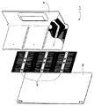
以下、本発明の実施の形態を図面に基づいて説明する。ここでは、圧電素子を用いた記録ヘッド(液体噴射ヘッドの一種)を例に挙げて説明する。図1に示すように、この記録ヘッド1は、流路ユニット2と、複数のアクチュエータユニット3…と、フィルム状の配線基板4とから概略構成されている。そして、流路ユニット2の表面に各アクチュエータユニット3…を横並びに接合し、流路ユニット2とは反対側のアクチュエータユニット3の表面に配線基板4を取り付けている。
【0032】
流路ユニット2は、図2の断面図に示すように、オリフィスとして機能するインク供給口5及びノズル連通口6の一部となる通孔を開設した供給口形成基板7と、共通インク室(共通液室の一種)8となる通孔及びノズル連通口6の一部となる通孔を開設したインク室形成基板9と、複数のノズル開口10…を開設したノズルプレート11から構成されている。これらの供給口形成基板7、インク室形成基板9、及び、ノズルプレート11は、例えば、ステンレス製の板材をプレス加工することで作製されている。なお、本実施形態では1つの流路ユニット2に3つのアクチュエータユニット3…が接合されているので、インク供給口5、ノズル連通口6、供給口形成基板7、共通インク室8等は、アクチュエータユニット3毎に合計3組形成されている。
【0033】
そして、流路ユニット2は、インク室形成基板9の一方の表面(図中下側)にノズルプレート11を、他方の表面(同上側)に供給口形成基板7をそれぞれ配置し、これらの供給口形成基板7、インク室形成基板9、及び、ノズルプレート11を接合することで作製される。例えば、シート状の接着剤によって各部材を接着することで作製される。
【0034】
上記のノズル開口10は、図3に示すように、所定ピッチで複数個列状に開設される。そして、列設された複数のノズル開口10…によってノズル列12が構成される。例えば、92個のノズル開口10…で1つのノズル列12が構成される。また、このノズル列12は、1つのアクチュエータユニット3に対して2列形成される。本実施形態の記録ヘッド1は3つのアクチュエータユニット3…を備えているため、合計6列のノズル列12…が横並びに形成される。
【0035】
アクチュエータユニット3は、ヘッドチップとも呼ばれる部材である。このアクチュエータユニット3は、図2に示すように、圧力室21となる通孔(本発明における空部の一種)を開設した圧力室形成基板22と、圧力室21の一部を区画する振動板23と、供給側連通口24となる通孔及びノズル連通口6の一部となる通孔を開設した蓋部材25と、振動板23の表面に形成されて駆動源として機能する圧電素子26とによって構成される。これら各部材22,23,25の板厚に関し、圧力室形成基板22、及び、蓋部材25は好ましくは50μm以上、より好ましくは100μm以上であり、振動板23は好ましくは3〜12μm程度であり、本実施形態では4〜6μmである。
【0036】
なお、このアクチュエータユニット3において、圧力室形成基板22、振動板23、及び、圧電素子26が本発明の圧電アクチュエータユニットとして機能する。また、振動板23と圧電素子26が圧電アクチュエータを構成し、振動板23が圧電素子26が設けられる支持基板の一種となる。
【0037】
このアクチュエータユニット3を作製するにあたり、まず、圧力室形成基板22の一方の表面に蓋部材25を、他方の表面に振動板23をそれぞれ配置し、これらの各部材22,23,25を一体化する。これらの圧力室形成基板22、振動板23、及び、蓋部材25は、アルミナや酸化ジルコニウム等のセラミックスで作製されている。例えば、グリーンシート(未焼成のシート材)に対して切削や打ち抜き等の加工を施して必要な通孔等を形成し、圧力室形成基板22、振動板23、及び、蓋部材25の各シート状前駆体を形成する。そして、各シート状前駆体を積層及び焼成することにより、各シート状前駆体は一体化されて1枚のシート状部材となる。そして、焼成後のシート状部材に対して圧電素子26等を形成することでセラミックスシートが作製される。
【0038】
この場合において、各シート状前駆体や圧電素子26は焼成により一体化されるので、特別な接着処理が不要である。また、各部材の接合面において高いシール性を得ることもできる。
【0039】
なお、1枚のセラミックスシートには、複数ユニット分の圧力室21…やノズル連通口6…等が形成されている。換言すれば、このセラミックスシートは、各アクチュエータユニット3…に切断される前のアクチュエータユニット母部材となる。例えば、1つのアクチュエータユニット3となるチップ領域を1枚のセラミックスシート内にマトリクス状に複数設定し、圧電素子26等の必要な部材を各チップ領域内に形成した後にこのセラミックスシートをチップ領域毎に切断することで、複数のアクチュエータユニット3…が作製される。
【0040】
上記の圧力室21は、ノズル列12とは直交する方向に細長い空部であり、ノズル開口10…に対応する複数形成されている。即ち、図3に示すように、ノズル列方向に列設されている。そして、各圧力室21…の一端は、供給側連通口24及びインク供給口5を通じて共通インク室8に連通している。また、供給側連通口24とは反対側の圧力室21の他端は、ノズル連通口6を通じて対応するノズル開口10に連通する。さらに、この圧力室21の一部(上側表面)は、振動板23によって区画されている。
【0041】
上記の圧電素子26は、所謂撓み振動モードの素子であり、圧力室21とは反対側の振動板表面に圧力室21毎に形成される。この圧電素子26は、圧力室長手方向に細長いブロック状であり、素子幅方向に複数並べた状態で設けられる。そして、圧電素子26の長手方向一端に近接させて、共通電極の一部を構成する共通幹電極27をノズル列方向に延設している。また、圧電素子26の長手方向他端に近接させて供給端子28…を設けている。この供給端子28は、配線基板4の接点端子(図示せず)が導通される部材であり、圧電素子26毎に設けられる。
【0042】
本実施形態における圧電素子26は、図5に示すように、圧電体層31と共通枝電極32と駆動電極33等によって構成される多層構造であり、駆動電極33と共通枝電極32とによって圧電体層31を挟んでいる。なお、この圧電素子26の構造については、後で詳しく説明する。
【0043】
そして、駆動電極33には供給端子28を通じて駆動信号の供給源(図示せず)が導通され、共通枝電極32は共通幹電極27等を通じて例えば接地電位に調整される。この駆動電極33に駆動信号が供給されると、駆動電極33と共通枝電極32との間には電位差に応じた強さの電場が発生される。この電場を圧電体層31に付与すると、圧電体層31は電場の強さに応じて変形する。即ち、駆動電極33の電位を高くする程、圧電体層31は電場と直交する方向に収縮し、圧力室21の容積を少なくするように振動板23を変形させる。一方、駆動電極33の電位を低くする程、圧電体層31は電界と直交する方向に伸長し、圧力室21の容積を増やすように振動板23を変形させる。
【0044】
このアクチュエータユニット3と上記の流路ユニット2とは、互いに接合される。例えば、供給口形成基板7と蓋部材25との間にシート状接着剤を介在させ、この状態でアクチュエータユニット3を流路ユニット2側に加圧することで接着される。
【0045】
上記構成の記録ヘッド1は、共通インク室8からインク供給口5、供給側連通口24、圧力室21、及び、ノズル連通口6を通じてノズル開口10に至る一連のインク流路がノズル開口10毎に形成されている。使用時においてこのインク流路内はインク(液体状のインクであり、本発明の液体の一種。)で満たされており、圧電素子26を撓ませることで対応する圧力室21が収縮或いは膨張し、圧力室21内のインクに圧力変動が生じる。このインク圧力を制御することで、ノズル開口10からインク滴を吐出させることができる。例えば、定常容積の圧力室21を一旦膨張させた後に急激に収縮させると、圧力室21の膨張に伴ってインクが充填され、その後の急激な収縮によって圧力室21内のインクが加圧されてインク滴が吐出される。
【0046】
ここで、インク滴の吐出量や吐出速度、吐出方向等を安定化するためには、即ち、インク滴の吐出特性を安定化するためには、定常状態における圧力室21の容積(定常容積)を一定に保つ必要がある。この定常容積は、圧力室21の膨張代を規定するので、定常容積が変動してしまうとインク滴の吐出量や吐出速度等も変動してしまう。そして、吐出特性を安定化するためには、圧力室21における変形部分のコンプライアンス(即ち、振動板23及び圧電素子26の全体のコンプライアンス)を小さくし、定常状態におけるインク圧力の変動等の影響を受け難くすることが好ましい。
【0047】
また、インク滴を高い周波数で吐出させるためにも、この変形部分のコンプライアンスを小さくすることが好ましい。これは、コンプライアンスが小さいと圧電素子26の変形に対する応答性が向上するからである。さらに、従来よりも高い周波数での駆動に耐えるため、圧電素子26の剛性を従来よりも高める必要もある。
【0048】
このような観点から、本実施形態では、多層構造の圧電素子26を用いている。以下、この点について説明する。
【0049】
まず、圧電素子26の構造について詳細に説明する。図5に示すように、この圧電素子26は所謂ブロック状であり、その幅W(図7参照)は圧力室21の幅と略等しく、その長さは圧力室21の長さよりも多少長い。上記の圧電体層31は、互いに積層された上層圧電体(外側圧電体)34及び下層圧電体(内側圧電体)35から構成される。また、共通枝電極32は、共通上電極(共通外電極,本発明の第2の電極)36及び共通下電極(共通内電極,本発明の第3の電極)37から構成される。そして、これらの共通枝電極32と駆動電極(本発明の第1の電極)33とが電極層を構成する。
【0050】
なお、ここでいう「上(外)」或いは「下(内)」とは、振動板23を基準とした位置関係を示している。即ち、「上(外)」とあるのは振動板23から遠い側を示し、「下(内)」とあるのは振動板23に近い側を示している。
【0051】
上記の駆動電極33は個別電極として機能し、上層圧電体34と下層圧電体35の境界に形成される。また、共通上電極36及び共通下電極37は、共通幹電極27と共に共通電極を構成する。即ち、この共通電極は、共通幹電極27から複数の共通枝電極32(共通上電極36,共通下電極37)…が延出形成された櫛歯状に形成されている。そして、共通下電極37は駆動電極33とは反対側の下層圧電体35の下部であって振動板23との間に形成され、共通上電極36は駆動電極33とは反対側の上層圧電体34の上部に形成される。即ち、この圧電素子26は、振動板23側から、共通下電極37、下層圧電体35、駆動電極33、上層圧電体34、共通上電極36の順で積層された多層構造である。
【0052】
本実施形態における圧電体層31の厚さは、幅方向の中央部分にて、上層圧電体34と下層圧電体35の2層を合計して約17μmである。そして、共通枝電極32を含めた圧電素子26の全体の厚さは約20μmである。即ち、共通下電極37が約3μmであり、共通上電極36が約0.3μmである。ここで、共通上電極36が極めて薄いのは、圧電素子26の変形時に支障を来さないようにするためである。なお、駆動電極33は、約2μmの厚さを有するが、上層圧電体34と下層圧電体35との間に埋設されている。
【0053】
そして、従来の単層構造の圧電素子は素子全体の厚さが約15μmであるので、本実施形態では圧電素子26の厚さが増した分だけ変形部分のコンプライアンスが小さくなっている。これにより、インク圧力の変動等に起因する圧力室21容積の変動が抑えられると共に、圧電素子26を高い周波数で駆動しても変形部分を追従させることができる。
【0054】
上記の共通上電極36及び共通下電極37は、駆動信号に拘わらず一定の電位、例えば接地電位に調整される。上記の駆動電極33は、供給された駆動信号に応じて電位を変化させる。従って、駆動信号の供給によって、駆動電極33と共通上電極36との間、及び、駆動電極33と共通下電極37との間には、それぞれ向きが反対の電場が生じる。
【0055】
そして、これらの各電極を構成する材料としては、例えば、金属単体、合金、電気絶縁性セラミックスと金属との混合物等の各種導体が選択されるが、焼成温度において変質等の不具合が生じないことが要求される。本実施形態では、共通上電極36に金を用い、共通下電極37及び駆動電極33に白金を用いている。
【0056】
上記の上層圧電体34と下層圧電体35は共に、例えばジルコン酸チタン酸鉛(PZT)を主成分とする圧電材料によって作製されている。そして、上層圧電体34と下層圧電体35とは分極方向が反対である。このため、駆動信号印加時の伸縮方向が上層圧電体34と下層圧電体35とで揃い、支障なく変形することができる。即ち、上層圧電体34及び下層圧電体35は、駆動電極33の電位を高くする程に圧力室21の容積を少なくするように振動板23を撓ませ、駆動電極33の電位を低くする程に圧力室21の容積を増やすように振動板23を撓ませる。
【0057】
この場合において、圧電素子26は多層構造であるので、各圧電体層34,35に付与される電場は駆動電極33から共通上電極36までの距離、或いは、駆動電極33から共通下電極37までの距離によって規定される。このため、駆動電圧が同じであっても、単層構造の圧電素子よりも強い電場を各圧電体層34,35に付与できる。これにより、圧電素子26を効率よく変形させることができ、印加電圧に対する変形量を向上させることができる。
【0058】
また、本実施形態では、定常状態の圧力室容積を一定にするため、圧電素子26の長手方向両端部を、圧力室21の長手方向両端を越えて外側まで形成している。即ち、図5に示すように、下層圧電体35の長手方向両端部を圧力室21の長手方向両端よりも外側に延出させた状態で形成すると共に、上層圧電体34の長手方向両端部も圧力室21の長手方向両端よりも外側に延出させた状態で形成している。そして、圧力室21よりも長手方向外側に位置する圧電素子26の両端部(圧電体層31の両端部。以下、延出部ともいう。)は、圧力室形成基板22や蓋部材25によって支持される振動板23の非変形部で、この振動板23に接合される。詳しくは、共通下電極37等の電極層を介して一体化されている。
【0059】
このように、延出部を振動板23の非変形部で接合しているため、圧力室21の変形部分はその全体が振動板23と圧電素子26の2層構造となる。このため、変形部分のコンプライアンスが一層小さくなり、定常状態におけるインク圧力の変動をより受け難くなる。従って、圧力室21の容積は圧電素子26の撓み量によって規定され、一層精密な容積制御を行うことができる。
【0060】
なお、この構成では、変形部分が振動板23と圧電素子26の2層構造であるので変形し難くなるが、圧電素子26を多層構造としているので必要十分な変形量を得ることができる。
【0061】
また、本実施形態では、圧電素子26の形状、特に、長手方向端部の形状を工夫することにより、電極の断線等が生じ難いように構成している。以下、この点について詳細に説明する。
【0062】
まず、共通上電極36について説明する。図5及び図6に示すように、これらの共通上電極36と共通下電極37は、素子長手方向の外側に延出され、圧電素子26の端部を越えた位置で互いに導通されている。即ち、共通下電極37は振動板23の表面に共通幹電極27の形成位置まで一連に形成され、共通上電極36は上層圧電体34の素子長手方向の端面及び下層圧電体35の素子長手方向の端面を通って共通下電極37に積層される。そして、本実施形態では、この共通上電極36も共通幹電極27の形成位置まで一連に形成されている。
【0063】
従って、共通上電極36と共通下電極37とは、下層圧電体35の端部を越えた位置、即ち、振動板23における非変形部で互いに導通される。このため、これらの共通上電極36と共通下電極37との導通部分には機械的ストレスが掛かり難くなり、導通の信頼性を長期に亘って維持することができる。また、この導通領域において、振動板23の裏側(即ち、圧電素子形成面とは反対側)には圧力室形成基板22が位置し、この振動板23を支持する。このため、振動板23の平面性を圧力室21に対応する部分よりも高くすることができ、両電極36,37を一様に、即ち、欠損部を生じさせることなく形成することができる。その結果、両電極36,37の導通信頼性を高めることができ、歩留まりを向上させることができる。
【0064】
また、これらの共通上電極36と共通下電極37に関し、下層圧電体35よりも外側の部分が共通導通部(本発明の第1導通部)38として機能する。そして、この共通導通部38と共通幹電極27(本発明の幹電極)とが互いに導通される。即ち、この共通導通部38を通じて共通枝電極32(36,37)に共通電位を供給している。この共通導通部38は、振動板23の非変形部に形成されているので、共通幹電極27との導通信頼性を長期に亘って維持することができる。さらに、各圧電素子26…は、上記したように素子幅方向に複数並べて設けられており、各共通導通部38…の形状は同一である。このため、共通幹電極27を直線帯状の導体パターンで構成でき、作製が容易である。また、共通幹電極27には屈曲部が必要無いので断線等の問題も生じ難い。
【0065】
また、本実施形態では、共通導通部38側の圧電体層31の形状に関し、下層圧電体35の端部を上層圧電体34の端部よりも素子長手方向の外側に延出している。これは、共通上電極36の断線を防止するためである。即ち、この共通上電極36は、上層圧電体34の上部に形成されているので、共通下電極37に導通させるためには素子長手方向の端面にも一様に形成する必要がある。
【0066】
ここで、圧電素子26が多層構造であるため、素子全体の厚さが従来の単層構造の圧電素子よりも厚くなっている。また、圧電素子26の変形を効率よく行う観点から共通上電極36が極めて薄いので、上層圧電体34の端面と下層圧電体35の端面とを揃えてしまうと、電極材料の塗布方法を工夫する等しないと端面に共通上電極36を一様に形成することは困難である。
【0067】
そして、本実施形態のように、下層圧電体35の端部を上層圧電体34の端部よりも外側に延出して階段状に設けると、上下方向の厚さ(積層方向の厚さ)が1層分で済み、マスクパターンを振動板23の上方からあてて電極材料を塗布する所謂印刷法(厚膜印刷)であっても、共通上電極36を圧電体層表面に一様に形成できる。従って、簡単な方法で作製できて製造効率を高めることができるし、且つ、導通の信頼性も高めることができる。
【0068】
次に、駆動電極33について説明する。この駆動電極33も素子長手方向の外側(共通導通部38とは反対側の他側)に延出され、下層圧電体35よりも外側の部分を駆動導通部(本発明の第2導通部)39としている。そして、この駆動導通部39は供給端子28の形成位置まで一連に形成され、この供給端子28に導通されている。
【0069】
ここで、本実施形態では、供給端子28に導通される導通電極(本発明の第4の電極)40を振動板23の表面に形成しており、この導通電極40の表面に駆動導通部39を形成している。これは、駆動導通部39と供給端子28との導通信頼性を高めるためである。即ち、下層圧電体35の外側端面と振動板表面とは、倒V字状(図では略直角のL字状)に交差している。このような交差面に対して電極を構成する場合、交差部への電極材料の充填が不足しがちであり、断線となってしまう虞がある。
【0070】
そして、本実施形態のように予め振動板23の表面に導通電極40を形成しておき、この導通電極40の表面に駆動電極33を形成すると、駆動電極33と導通電極40の接触によって駆動電極33と供給端子28とが導通される。このため、導通の信頼性をより高めることができる。
【0071】
また、この導通電極40の素子長手方向についての形成領域、詳しくは、供給端子28とは反対側の先端の形成位置に関し、少なくとも下層圧電体35の先端まで形成されていれば上記した作用効果を奏する。そして、本実施形態では、この先端を、下層圧電体35の端面を越えて共通下電極37の手前に位置させている。なお、導通電極40と下層圧電体35との間には絶縁領域Xが設けられており、互いに電気的に絶縁されている。
【0072】
このように導通電極40の一部を下層圧電体35と振動板23の間に形成しているのは、各圧電素子26の形成位置の公差を考慮したためである。即ち、この圧電素子26の作製は、マスクを用いた印刷法で行われている。例えば、振動板23の表面に共通下電極37となる電極材料を所定のパターンで印刷した後に焼成し、次に下層圧電体35となる圧電材料を共通下電極37の上に積層されるように印刷して焼成する。以後は、同様な手順で、駆動電極33、上層圧電体34、共通上電極36の印刷及び焼成を順次行う。
【0073】
このように、圧電素子26が印刷法で形成されるので、下層圧電体35の端面が形成される位置には多少なりのばらつき(公差)が生じる。そこで、本実施形態では、導通電極40の一部を下層圧電体35と振動板23の間に形成し、下層圧電体35の形成位置が多少ばらついても駆動電極33と導通電極40とが確実に導通されるように構成している。
【0074】
また、この導通電極40は種々の電極材料で形成することができるが、共通下電極37と同一の電極材料を用いることが好ましい。これは、製造効率を向上させるためである。上記したように、この圧電素子26は、電極材料や圧電材料の印刷及び焼成を繰り返すことで作製される。そして、導通電極40を共通下電極37と同一の電極材料で形成すると、共通下電極37の形成と導通電極40の形成とを一度に行うことができる。即ち、1つのマスクパターンに共通下電極37のパターンと導通電極40のパターンとを形成することで、共通下電極37と導通電極40とを同じ工程で纏めて作製できる。従って、製造効率を向上させることができる。
【0075】
また、本実施形態では、共通枝電極32や駆動電極33の形成範囲や圧電素子26における幅方向の形状を工夫することにより、変形効率を高めるように構成している。以下、この点について詳細に説明する。
【0076】
まず、共通枝電極32や駆動電極33の形成範囲について説明する。本実施形態では、駆動電極33、共通上電極36及び共通下電極37の各電極を、圧力室21の長手方向を覆うように一連に形成している。即ち、図5及び図6に示すように、駆動電極33に関しては、その長さを圧力室21よりも長く設定し、供給端子28(駆動導通部39)から遠い側の圧力室端面を越えた位置まで一連に形成している。また、共通上電極36及び共通下電極37に関しても、その長さを圧力室21よりも長く設定し、共通幹電極27(共通導通部38)から遠い側の圧力室端面を越えた位置まで一連に形成している。これにより、これらの各電極の重畳領域、即ち、圧電体層31が変形し得る活性領域LAの内側に圧力室21が位置する。言い換えれば、電極積層方向から見て活性領域LAの範囲内に圧力室21が重畳した状態となる。
【0077】
このように、活性領域LAの範囲内に圧力室21が位置すると、上記した変形部分はその全体(即ち、圧力室21を区画する部分)で撓む。言い換えれば、振動板23の非変形部よりも内側の圧力室21の範囲内で撓む。これにより、圧力室21の容積変化量を可及的に大きくすることができ、インク滴の吐出量増加や高粘度のインクの吐出に寄与する。
【0078】
なお、この例では、共通上電極36と共通下電極37の両方が圧力室21の長手方向を覆うように形成されていたが、少なくとも一方の電極が圧力室21の長手方向を覆うように形成されていればよい。また、各電極は、圧力室21の端面を越えて一連に形成されていたが、電極積層方向から見て圧力室21の端面と面一となる位置まで形成されていれば同様の効果を奏する。
【0079】
次に、圧電素子26における幅方向の形状について説明する。本実施形態では、駆動電極33よりも幅方向外側に位置する幅端部領域の厚さを、駆動電極33の幅内に位置する幅中央領域の厚さよりも薄くしている点に特徴がある。
【0080】
図7は圧電素子26を電極幅方向(短尺方向)に切断した図である。この圧電素子26では、下層圧電体35により共通下電極37をその全幅を越えて覆うと共に、上層圧電体34により駆動電極33をその全幅を越えて覆っている。従って、駆動電極33は、その大部分が両圧電体層34,35内に埋設された状態となる。また、駆動電極33と共通下電極37との間には電気絶縁性を有する下層圧電体35が存在するので、駆動電極33と共通下電極37との短絡を確実に防止することもできる。
【0081】
この圧電素子26では、駆動電極33よりも幅方向外側に位置する幅端部領域WL,WRの厚さを、駆動電極33の幅内に位置する幅中央領域WCの厚さよりも薄く構成している。ここで、幅中央領域WCは、駆動電極33の幅方向両端のそれぞれから上下方向に設定される一対の第1仮想線L1,L1の範囲内の部分である。また、幅端部領域WL,WRは、この第1仮想線L1よりも幅方向外側の部分である。さらに、図7において、幅中央領域WCよりも左側の部分を左幅端部領域WLとし、幅中央領域WCよりも右側の部分を右幅端部領域WRとする。
【0082】
そして、上左端領域34Lの厚さ及び上右端領域34Rの厚さを上幅中央領域34Cの厚さよりも薄く設定し、下左端領域35Lの厚さ及び下右端領域35Rの厚さを下幅中央領域35Cの厚さよりも薄く設定すると、幅端部領域WL,WRにおける各圧電体層34,35の応力が幅中央領域WCにおける各圧電体層34,35の応力よりも小さくなる。このため、幅端部領域WL,WRの部分が幅中央領域WCの部分よりも撓み易くなり、圧電素子26を効率よく変形させることができる。
【0083】
ところで、本発明は、上記実施形態に限定されるものではなく、特許請求の範囲の記載に基づいて種々の変形が可能である。
【0084】
例えば、図8に示す変形例のように、上層圧電体34´の全長を下層圧電体35´の全長よりも長く設定し、上層圧電体34´によって下層圧電体35´の長手方向両端を越えて覆うように構成してもよい。
【0085】
このように、上層圧電体34´で下層圧電体35´を覆うと、共通導通部38側に関しては、上層圧電体34´の端部表面が比較的なだらかな傾斜面(彎曲面)を構成する。即ち、共通上電極36の形成面に段差等が生じ難くなり、滑らかに設けることができる。これにより、共通上電極36を上層圧電体34´の端部表面に一様に設けることができ、欠損部の発生等を防止できて製造上の信頼性を高めることができる。そして、上層圧電体34´の端部表面を滑らかに構成するという観点からすれば、下層圧電体35´における長手方向端部の厚さを、長手方向先端に向かう程薄くすることが好ましい。
【0086】
一方、駆動電極33側に関しては、導通電極40と駆動電極33とが重なる場所、具体的には、下層圧電体35´を越えてすぐの場所で上層圧電体34´が駆動電極33を覆う。これにより、上層圧電体34´の先端部分が駆動電極33の保護層としても機能し、駆動電極33の劣化や剥離を防止し、駆動電極33と導通電極40の導通状態をより確実なものとすることができる。そして、この駆動電極33側に関しても下層圧電体35´における長手方向端部の厚さを、長手方向先端に向かう程薄くすることが好ましい。これは、駆動電極33と導通電極40とを確実に導通させるためである。即ち、下層圧電体35´の端部を漸次薄く構成することで、下層圧電体35´の端面がなだらかな傾斜面となり、駆動電極33を一様に設けることが容易になる。これにより、製造上の信頼性を高めることができる。
【0087】
そして、この変形例の圧電素子26を作製するにあたっては、印刷パターン(即ち、開口部)の形状が異なる2種類のマスクを用いるのが簡便でよい。例えば、図9に示すように、下層圧電体35´に対応する細長い印刷パターンP1を複数設けた第1のマスクM1と、上層圧電体34´に対応する細長い印刷パターンP2を複数設けた第2のマスクM2とを用いる。
【0088】
ここで、印刷パターンP1は、その長さPL1が下層圧電体35´の素子長手方向の長さに設定され、その幅PWが圧電素子26の幅に設定された矩形状(細長い帯状)の開口部であり、その幅方向に複数並べられた状態で設けられている。また、印刷パターンP2は、その長さPL2が上層圧電体34´の素子長手方向の長さに設定され、その幅PWが圧電素子26の幅に設定された矩形状の開口部である。言い換えると、この印刷パターンP2は、その長さPL2が印刷パターンP1の長さPL1よりも長く、その幅PWが印刷パターンP1と同じ幅に設定された矩形状の開口部である。そして、この印刷パターンP2も、印刷パターンP1と同様に、その幅方向に複数並べられた状態で設けられている。
【0089】
次に、これらのマスクM1,M2を用いて変形例の圧電素子26を作製する手順について説明する。
【0090】
この場合、まず、共通下電極形成工程にて共通下電極37を焼成後のシート状部材に形成する。例えば、焼成後のシート状部材における振動板表面に、共通下電極37及び導通電極40用の印刷パターンを設けたマスクを載置し、このマスクを介してペースト状の電極材料を振動板表面に塗布する。電極材料を塗布したならば、この電極材料を焼成して共通下電極37及び導通電極40を形成する。
【0091】
これらの共通下電極37及び導通電極40を形成したならば、下層圧電体形成工程に移行して下層圧電体35を形成する。この下層圧電体形成工程では、これらの電極37,40上に印刷パターンP1が重なるように第1のマスクM1を載置し、このマスクを介してペースト状の圧電材料を塗布する。これらの電極37,40上に圧電材料を塗布したならば、この圧電材料を焼成して下層圧電体35´を形成する。
【0092】
下層圧電体35´を形成したならば、駆動電極形成工程(本発明の第1電極形成工程)に移行して駆動電極33を形成する。この駆動電極形成工程では、下層圧電体35´上に駆動電極用の印刷パターンが重なるようにマスクを載置し、このマスクを介してペースト状の電極材料を塗布する。そして、これらの下層圧電体35´上に電極材料を塗布したならば、この電極材料を焼成して駆動電極33を形成する。
【0093】
駆動電極33を形成したならば、上層圧電体形成工程に移行して上層圧電体34´を形成する。この上層圧電体形成工程では、下層圧電体35´の長手方向両端が印刷パターンP2の長手方向内側に収まるように第2のマスクM2を載置し、このマスクM2を介してペースト状の圧電材料を塗布する。即ち、塗布した圧電材料によって下層圧電体35´の長手方向両端が埋設されるように覆う。そして、圧電材料を塗布したならば、この電極材料を焼成して上層圧電体34´を形成する。
【0094】
以後は、同様な手順で、共通上電極36,共通幹電極27,供給端子28等を形成する。この場合において、上層圧電体34´により下層圧電体35´の長手方向両端を覆っているので、上記したように、上層圧電体34´の両端部表面が比較的滑らかになり、共通上電極36を一様に(必要な所に欠損なく)設けることができる。また、駆動電極33を上方から覆うので、駆動電極33と導通電極40の電気的導通の信頼性を高めることができる。
【0095】
また、図10(a)に示すように、供給端子28を端子基板41上に形成し、導通電極40´の供給端子28側の部分を端子基板41上に形成してもよい。この場合において、端子基板41は導電性を有する焼成材料、例えば、銀ペーストを用いて作製することが好ましい。
【0096】
また、この図に示すように、供給端子28側については、上層圧電体34の端面と下層圧電体35の端面を面一に形成してもよい。
【0097】
また、図10(b)に示すように、共通幹電極27(共通導通部38)側に関し、下層圧電体35における素子長手方向外側の端面と上層圧電体34における素子長手方向外側の端面とを一連の傾斜面Yによって構成してもよい。このように構成すると、断線の要因となり得る凹凸(段差)が生じ難いので、共通上電極36をこの傾斜面Y上に一様に形成し易い。従って、駆動導通部38(共通上電極36)の断線防止に寄与する。
【0098】
なお、以上は、液体噴射ヘッドの一種である記録ヘッド1を例に挙げて説明したが、本発明は、液晶噴射ヘッドや色材噴射ヘッド等といった他の液体噴射ヘッド、或いは、これらの液体噴射ヘッドに用いられる圧電アクチュエータユニット及び圧電素子にも適用できる。また、マイクロポンプ等の各種装置に用いられる圧電アクチュエータユニット及び圧電素子にも適用することができる。
【0099】
【発明の効果】
以上説明したように、本発明によれば以下の効果を奏する。
【0100】
即ち、互いに積層された上層圧電体と下層圧電体とを有し、これらの上層圧電体と下層圧電体の間には圧電素子の長手方向一方の端面から所定間隔をあけて第1の電極を形成し、上層圧電体の表面には第2の電極を形成し、下層圧電体と振動板の間には第3の電極を形成した多層構造の圧電素子を用い、下層圧電体の長手方向両端部を圧力室両端よりも外側に延出させた状態で形成すると共に、上層圧電体の長手方向両端部も圧力室両端よりも外側に延出させた状態で形成したので、振動板と圧電素子とで構成される圧力室の変形部分のコンプライアンスを小さくすることができ、定常状態における圧力室容積の変動を確実に抑えることができる。これにより、液体の吐出特性や送出特性を安定化することができる。また、変形部分のコンプライアンスを小さくすることができることから高周波駆動にも適する。
また、第2の電極の圧電素子の前記端面を通って伸びる部分と前記第3の電極との導通部分を、振動板の圧力室に対向する領域とは異なる領域であって当該振動板上に設けたので、導通部分には機械的ストレスが掛かり難くなり、導通の信頼性を長期に亘って維持することができる。さらに、この導通部分において、振動板の裏側(即ち、圧電素子形成面とは反対側)には圧力室形成基板が位置し、この振動板を支持する。このため、振動板の平面性を圧力室に対応する部分よりも高くすることができ、両電極を一様に、即ち、欠損部を生じさせることなく形成することができる。その結果、両電極の導通信頼性を高めることができ、歩留まりを向上させることができる。
【0101】
さらに、圧電素子が多層構造であるので変形効率を高めることができる。これにより、コンプライアンスの減少に起因する変形部分の変形量減少を補うことができる。従って、高周波駆動しつつも必要量の液体を吐出或いは送液することができる。
【0102】
また、下層圧電体の第1導通部の端部を、同じ側に位置する上層圧電体の端部よりも素子長手方向の外側に延出した場合には、第2の電極の断線防止が図れ、歩留まりの向上が図れる。
【0103】
また、上層圧電体の全長を下層圧電体の全長よりも長く設定し、上層圧電体により下層圧電体の長手方向両端を越えて覆った場合には、上層圧電体における第2の電極形成面に段差等が生じ難くなり、滑らかに設けることができる。これにより、第2の電極を一様に設けることができ、欠損部の発生等を防止できて製造上の信頼性を高めることができる。
【0104】
また、第2の電極と第3の電極を素子長手方向の外側に延出して互いに導通させると共に、これらの電極における下層圧電体よりも外側の部分を第1導通部とし、第1の電極を第1導通部とは反対側となる素子長手方向の外側に延出した場合、及び、第1の電極における下層圧電体よりも外側の部分を第2導通部とした場合には、第1導通部や第2導通部を変形部分から外れた非変形部に形成できる。このため、当該部分に端子や電極を設けて導通させても、その導通部分の接続信頼性を長期間に亘って維持することができる。
【0105】
また、供給端子に導通される第4の電極を振動板表面に形成し、該第4の電極の表面に第2導通部を形成した場合には、第2導通部の断線防止が図れ、歩留まりの向上が図れる。
【0106】
また、第2の電極と第3の電極の少なくとも一方の電極と第1の電極とを、圧力室がその長手方向に覆われる位置まで一連に形成した場合には、圧力室の変形部分全体を変形させることができ、必要な吐出量(送液量)が確保できる。
【0107】
また、下層圧電体により第3の電極をその全幅を越えて覆うと共に、前記上層圧電体により第1の電極をその全幅を越えて覆い、上層圧電体と下層圧電体の少なくとも一方について、第1の電極よりも幅方向外側に位置する幅端部領域の厚さを、第1の電極の幅内に位置する幅中央領域の厚さよりも薄くした場合には、変形部分における変形効率を高めることができ、必要な吐出量(送液量)が確保できる。
【図面の簡単な説明】
【図1】 記録ヘッドの構成を説明する分解斜視図である。
【図2】 アクチュエータユニット及び流路ユニットを説明する断面図である。
【図3】 ノズルプレートを説明する部分拡大図である。
【図4】 アクチュエータユニットを圧電素子側から見た斜視図である。
【図5】 (a)は圧電素子の平面図、(b)は長手方向に切断した圧電素子の断面図である。
【図6】 (a)は供給端子側の圧電素子の端部構造を示す部分拡大断面図、(b)は共通幹電極側の圧電素子の端部構造を示す部分拡大断面図である。
【図7】 (a),(b)は、圧電素子を幅方向に切断した断面図である。
【図8】 変形例を説明する図であり、(a)は供給端子側の圧電素子の端部構造を示す部分拡大断面図、(b)は共通幹電極側の圧電素子の端部構造を示す部分拡大断面図である。
【図9】 (a)及び(b)は、変形例の圧電素子を作製する際に用いるマスクを説明する図である。
【図10】 他の変形例を説明する図であり、(a)は、供給端子側の圧電素子の端部構造を示す部分拡大断面図(b)は、共通幹電極側の圧電素子の端部構造を示す部分拡大断面図である。
【符号の説明】
1 記録ヘッド
2 流路ユニット
3 アクチュエータユニット
4 配線基板
5 インク供給口
6 ノズル連通口
7 供給口形成基板
8 共通インク室
9 インク室形成基板
10 ノズル開口
11 ノズルプレート
12 ノズル列
21 圧力室
22 圧力室形成基板
23 振動板
24 供給側連通口
25 蓋部材
26 圧電素子
27 共通幹電極
28 供給端子
31 圧電体層
32 共通枝電極
33 駆動電極
34,34´ 上層圧電体
35,35´ 下層圧電体
36 共通上電極
37 共通下電極
38 共通導通部
39 駆動導通部
40,40´ 導通電極
41 端子基板[0001]
BACKGROUND OF THE INVENTION
The present invention relates to a piezoelectric actuator unit that uses a piezoelectric element that is deformed by supply of a driving signal as a driving source, and a liquid ejecting head that includes the piezoelectric actuator unit.
[0002]
[Prior art]
Piezoelectric actuator unit is a piezoelectric material consisting of piezoelectric ceramics that compress and fire metal oxide powders such as BaTiO3, PbZrO3, and PbTiO3, or piezoelectric polymer films that use polymer compounds, which are piezoelectric materials that exhibit a piezoelectric effect. Is a member that changes the volume of the pressure chamber by bending the diaphragm by deformation of the piezoelectric element, and is suitably used as, for example, a component of a liquid ejecting head or a micropump. Here, the liquid ejecting head ejects liquid droplets from the nozzle openings. For example, the liquid ejecting head is used for manufacturing a recording head used for an image recording apparatus such as a printer, a liquid crystal ejecting head used for manufacturing a liquid crystal display, and a color filter. There are color material ejection heads used. The micropump is an ultra-compact pump that can handle a very small amount of liquid.
[0003]
The diaphragm is a very thin member having a thickness of about 5 to 6 μm, and the piezoelectric element has a single-layer structure in practical use and has a thickness of about 15 μm. Therefore, the total thickness of the diaphragm and the piezoelectric element is about 20 μm. For this reason, the compliance of the deformed portion in the pressure chamber, that is, the compliance of the vibration plate and the piezoelectric element is large, and the volume may change due to a slight change in the liquid pressure existing in the pressure chamber. Further, when the compliance of the deformed portion is large, the responsiveness (deformation responsiveness) of the piezoelectric element to the supplied drive signal is deteriorated, and high-frequency driving becomes difficult.
[0004]
Here, it is conceivable to make the piezoelectric element thicker than before in order to reduce the compliance of the deformed part, but simply increasing the thickness requires a higher drive voltage, making it unsuitable for high-frequency driving. End up. In addition, since the deformed portion is difficult to bend, the amount of pressure fluctuation of the liquid is insufficient.
[0005]
Therefore, JP-A-2-289352(Patent Document 1)And JP-A-10-34924(Patent Document 2)It is conceivable to use a piezoelectric element having a multilayer structure disclosed in the above. In this piezoelectric element, the piezoelectric layer has a two-layer structure of an upper layer piezoelectric material and a lower layer piezoelectric material, a drive electrode is formed at the boundary between the upper layer piezoelectric material and the lower layer piezoelectric material, and a common upper electrode is formed on the outer surface of the upper layer piezoelectric material. The common lower electrode is formed on the outer surface of the lower piezoelectric body.
[0006]
In this piezoelectric element, since the drive electrode is provided at the boundary between the upper layer piezoelectric body and the lower layer piezoelectric body, the piezoelectric element of each layer includes the distance from the drive electrode to each common electrode (the thickness of each layer piezoelectric body), An electric field having a strength determined by the potential difference between the drive electrode and each common electrode is applied. For this reason, when compared with a piezoelectric element having a single-layer structure in which a single-layer piezoelectric body is sandwiched between a common electrode and a drive electrode, that is, a piezoelectric element that has been put into practical use, the overall thickness of the piezoelectric element is slightly increased. Even if the rigidity is increased, it can be greatly deformed with the same driving voltage as in the prior art.
[0007]
[Patent Document 1]
JP-A-2-289352
[Patent Document 2]
Japanese Patent Laid-Open No. 10-34924
[0008]
[Problems to be solved by the invention]
However, it has been difficult to obtain desired characteristics simply by using the multilayered piezoelectric element described in each of the above publications. For example, liquid ejection characteristics and delivery characteristics vary, and the high-frequency driving of the piezoelectric element and the liquid ejection amount (delivery amount) cannot be balanced. Moreover, the problem that disconnection etc. occur easily in an electrode also arose. For this reason, as an actual product, it is necessary to use a single-layer piezoelectric element in which a single-layer piezoelectric body is sandwiched between a common electrode and a drive electrode.
[0009]
The present invention has been made in view of such circumstances, and its main object is to stabilize the liquid discharge (delivery) characteristics. Another object of the present invention is to obtain a necessary discharge amount (feed amount) while driving at high frequency. A further object of the present invention is to increase manufacturing reliability and improve yield.
[0010]
[Means for Solving the Problems]
The present invention has been proposed in order to achieve the above-mentioned object. According to the first aspect of the present invention, a diaphragm is provided on the surface of a pressure chamber forming substrate having an empty portion serving as a pressure chamber, thereby forming the pressure chamber. In a piezoelectric actuator unit formed by forming a piezoelectric element at a position corresponding to the pressure chamber on the surface of the diaphragm opposite to the substrate,
The piezoelectric element has an upper layer piezoelectric body and a lower layer piezoelectric body that are stacked on each other, and between these upper layer piezoelectric body and lower layer piezoelectric body.At a predetermined interval from one end face in the longitudinal direction of the piezoelectric elementA first electrode is formed, a second electrode is formed on the surface of the upper layer piezoelectric body, and a third electrode is formed between the lower layer piezoelectric body and the diaphragm.
The lower piezoelectric element is formed with both longitudinal ends extending outward from both ends of the pressure chamber, and the upper piezoelectric element is formed with both longitudinal ends extending outward from both ends of the pressure chamber. And
The second electrodeA portion extending through the end face of the piezoelectric elementThe piezoelectric actuator unit is characterized in that a conductive portion between the first electrode and the third electrode is provided on the vibration plate in a region different from a region facing the pressure chamber of the vibration plate.
[0011]
Here, “upper and lower” indicates a positional relationship based on a support substrate such as a diaphragm. That is, the side closer to the support substrate is indicated as “lower”, and the side farther from the support substrate is indicated as “upper”. The “position corresponding to the pressure chamber” means a position where the piezoelectric element and the pressure chamber overlap each other when viewed from the stacking direction of the pressure chamber forming substrate, the vibration plate, and the piezoelectric element.
[0012]
What is claimed in claim 2The conductive portion is laminated on a portion of the second electrode that extends through the end face of the piezoelectric element and a portion of the third electrode that extends through the end face of the piezoelectric element.The piezoelectric actuator unit according to
[0013]
In the third aspect, the lower piezoelectric bodyAboveIn the end face and upper layer piezoelectric materialAbove3. The piezoelectric actuator unit according to
[0017]
According to a fourth aspect of the present invention, the first electrode extends outward in the longitudinal direction of the element, and a portion outside the lower layer piezoelectric body of the first electrode is used as a second conductive portion. The piezoelectric actuator unit according to any one of
[0018]
According to a fifth aspect of the present invention, in the piezoelectric actuator unit according to the fourth aspect of the present invention, a fourth electrode that is electrically connected to the second conductive portion is formed on the surface of the diaphragm.
[0019]
According to a sixth aspect of the present invention, in the piezoelectric actuator unit according to the fifth aspect, the fourth electrode is electrically connected to a supply terminal for supplying an external drive signal.
[0020]
According to a seventh aspect of the present invention, a part of the fourth electrode opposite to the supply terminal is formed between the lower layer piezoelectric body and the diaphragm, and the piezoelectric according to the fifth or sixth aspect Actuator unit.
[0021]
The piezoelectric device according to any one of
[0022]
According to a ninth aspect of the present invention, at least one of the second electrode and the third electrode and the first electrode are formed in series until the position where the pressure chamber is covered in the longitudinal direction. The piezoelectric actuator unit according to any one of
[0023]
Note that “up to the position covered in the longitudinal direction” means that the tip of each electrode is formed to substantially the same position as the end face in the longitudinal direction of the pressure chamber when viewed from the electrode stacking direction, and the length of the pressure chamber It includes both of the state where it is formed beyond the end face in the direction to the outside.
[0024]
According to a tenth aspect of the present invention, the third electrode is covered with the lower piezoelectric body over the entire width thereof, and the first electrode is covered with the upper piezoelectric body over the entire width thereof,
For at least one of the upper layer piezoelectric material and the lower layer piezoelectric material, the thickness of the width end region located outside the first electrode in the width direction is set to be larger than the thickness of the width center region located within the width of the first electrode. The piezoelectric actuator unit according to any one of
[0025]
An eleventh aspect of the present invention is the piezoelectric actuator unit according to any one of the first to tenth aspects, wherein a plurality of the piezoelectric elements are arranged in the width direction.
[0026]
According to a twelfth aspect of the present invention, in the piezoelectric actuator unit according to the eleventh aspect, the first conductive portions of the piezoelectric elements are electrically connected to each other by a trunk electrode extending in the width direction of the piezoelectric elements. is there.
[0027]
According to a thirteenth aspect of the present invention, a vibration plate is provided on the surface of a pressure chamber forming substrate having an empty portion serving as a pressure chamber, and corresponds to the pressure chamber on the surface of the vibration plate opposite to the pressure chamber forming substrate. A piezoelectric actuator unit formed by forming a piezoelectric element at a position;
A nozzle opening communicated with the pressure chamber via the nozzle communication port, and a flow path unit having at least a common liquid chamber communicated with the pressure chamber via the liquid supply port,
A liquid ejecting head in which a pressure change is generated in the liquid in the pressure chamber by deformation of the piezoelectric element, and droplets are ejected from the nozzle opening using the pressure fluctuation,
A liquid ejecting head, wherein the piezoelectric actuator unit includes the piezoelectric actuator unit according to any one of
[0031]
DETAILED DESCRIPTION OF THE INVENTION
Hereinafter, embodiments of the present invention will be described with reference to the drawings. Here, a recording head using a piezoelectric element (a kind of liquid ejecting head) will be described as an example. As shown in FIG. 1, the
[0032]
As shown in the cross-sectional view of FIG. 2, the
[0033]
The
[0034]
As shown in FIG. 3, the
[0035]
The
[0036]
In the
[0037]
In producing the
[0038]
In this case, since each sheet-like precursor and the
[0039]
A single ceramic sheet is formed with a plurality of units of
[0040]
The
[0041]
The
[0042]
As shown in FIG. 5, the
[0043]
A drive signal supply source (not shown) is conducted to the
[0044]
The
[0045]
In the
[0046]
Here, in order to stabilize the ejection amount, ejection speed, ejection direction, and the like of the ink droplets, that is, to stabilize the ejection characteristics of the ink droplets, the volume of the
[0047]
In order to eject ink droplets at a high frequency, it is preferable to reduce the compliance of the deformed portion. This is because the response to deformation of the
[0048]
From such a viewpoint, in the present embodiment, the multilayered
[0049]
First, the structure of the
[0050]
Here, “upper (outer)” or “lower (inner)” indicates a positional relationship with respect to the
[0051]
The
[0052]
The thickness of the
[0053]
Since the conventional single layer structure piezoelectric element has a total thickness of about 15 μm, in this embodiment, the compliance of the deformed portion is reduced by the increase in the thickness of the
[0054]
The common
[0055]
And as materials constituting these electrodes, for example, various conductors such as simple metals, alloys, and mixtures of electrically insulating ceramics and metals are selected, but defects such as alteration are not caused at the firing temperature. Is required. In the present embodiment, gold is used for the common
[0056]
Both the upper layer
[0057]
In this case, since the
[0058]
Further, in the present embodiment, in order to make the pressure chamber volume in a steady state constant, both longitudinal ends of the
[0059]
As described above, since the extending portion is joined by the non-deformed portion of the
[0060]
In this configuration, since the deformed portion has a two-layer structure of the
[0061]
In the present embodiment, the shape of the
[0062]
First, the common
[0063]
Accordingly, the common
[0064]
In addition, regarding the common
[0065]
Further, in the present embodiment, with respect to the shape of the
[0066]
Here, since the
[0067]
Then, as in the present embodiment, when the end portion of the lower
[0068]
Next, the
[0069]
Here, in this embodiment, a conducting electrode that is conducted to the supply terminal 28.(Fourth electrode of the present invention)40 is formed on the surface of the
[0070]
Then, when the
[0071]
In addition, regarding the formation region of the
[0072]
The reason why a part of the
[0073]
As described above, since the
[0074]
The
[0075]
In the present embodiment, the deformation efficiency is improved by devising the formation range of the
[0076]
First, the formation range of the
[0077]
As described above, when the
[0078]
In this example, both the common
[0079]
Next, the shape of the
[0080]
FIG. 7 is a diagram in which the
[0081]
In the
[0082]
Then, the thickness of the upper
[0083]
By the way, the present invention is not limited to the above-described embodiment, and various modifications can be made based on the description of the scope of claims.
[0084]
For example, as in the modification shown in FIG. 8, the total length of the upper layer piezoelectric body 34 'is set longer than the total length of the lower layer piezoelectric body 35', and the upper layer piezoelectric body 34 'crosses both longitudinal ends of the lower layer piezoelectric body 35'. You may comprise so that it may cover.
[0085]
As described above, when the lower
[0086]
On the other hand, with respect to the
[0087]
In producing the
[0088]
Here, the printing pattern P1 has a rectangular (elongated strip-shaped) opening in which the length PL1 is set to the length in the element longitudinal direction of the lower layer piezoelectric body 35 'and the width PW is set to the width of the
[0089]
Next, a procedure for manufacturing the
[0090]
In this case, first, the common
[0091]
If the common
[0092]
Once the lower piezoelectric body 35 'is formed, a drive electrode forming step(First electrode forming step of the present invention)Then, the
[0093]
When the
[0094]
Thereafter, the common
[0095]
10A, the
[0096]
Further, as shown in this figure, on the
[0097]
Further, as shown in FIG. 10B, with respect to the common trunk electrode 27 (common conductive portion 38) side, an end face on the outer side in the element longitudinal direction of the lower
[0098]
In the above, the
[0099]
【The invention's effect】
As described above, the present invention has the following effects.
[0100]
That is, it has an upper layer piezoelectric material and a lower layer piezoelectric material laminated together, and between these upper layer piezoelectric material and lower layer piezoelectric material.At a predetermined interval from one end face in the longitudinal direction of the piezoelectric elementA first electrode is formed, a second electrode is formed on the surface of the upper layer piezoelectric body, and a multilayered piezoelectric element in which a third electrode is formed between the lower layer piezoelectric body and the diaphragm is used. Since both ends in the longitudinal direction are extended outward from both ends of the pressure chamber, and the both ends in the longitudinal direction of the upper piezoelectric body are also extended outward from both ends of the pressure chamber, the diaphragm And the compliance of the deformed portion of the pressure chamber composed of the piezoelectric element can be reduced, and the fluctuation of the pressure chamber volume in the steady state can be surely suppressed. Thereby, the discharge characteristic and delivery characteristic of a liquid can be stabilized. Further, since the compliance of the deformed portion can be reduced, it is also suitable for high frequency driving.
The second electrodeThe portion extending through the end face of the piezoelectric elementAnd the third electrode are provided on the diaphragm in a region different from the region facing the pressure chamber of the diaphragm, so that mechanical stress is less likely to be applied to the conduction portion. Can be maintained over a long period of time. Further, in this conductive portion, a pressure chamber forming substrate is located on the back side of the diaphragm (that is, the side opposite to the piezoelectric element forming surface) and supports the diaphragm. For this reason, the flatness of the diaphragm can be made higher than that of the portion corresponding to the pressure chamber, and both electrodes can be formed uniformly, that is, without causing a defect portion. As a result, the conduction reliability of both electrodes can be increased, and the yield can be improved.
[0101]
Furthermore, since the piezoelectric element has a multilayer structure, the deformation efficiency can be increased. As a result, it is possible to compensate for a decrease in the deformation amount of the deformed portion due to a decrease in compliance. Therefore, a required amount of liquid can be discharged or fed while driving at a high frequency.
[0102]
Also, the lower layer piezoelectric1st conduction partWhen extending the end of the outer side of the element longitudinal direction from the end of the upper layer piezoelectric body located on the same side,Second electrodeCan be prevented and the yield can be improved.
[0103]
In addition, when the upper layer piezoelectric body is set to be longer than the entire length of the lower layer piezoelectric body and is covered by the upper layer piezoelectric body beyond both longitudinal ends of the lower layer piezoelectric body, the upper layer piezoelectric bodySecond electrode inA level difference or the like hardly occurs on the formation surface, and the surface can be provided smoothly. ThisSecond electrodeCan be provided uniformly, and the occurrence of a defective portion or the like can be prevented, and the manufacturing reliability can be improved.
[0104]
Also,Second electrodeWhenThird electrodeAre extended to the outside in the longitudinal direction of the element, and are connected to each other.1st conduction partage,First electrodeThe1st conduction partExtending to the outside in the longitudinal direction of the element on the opposite side, andFirst electrodeThe outer part of the lower piezoelectric body inSecond conduction partIf1st conduction partAndSecond conduction partCan be formed in a non-deformable portion that is out of the deformed portion. For this reason, even if a terminal or an electrode is provided in the part to make it conductive, the connection reliability of the conductive part can be maintained over a long period of time.
[0105]
Also conducted to the supply terminal4th electrodeOn the surface of the diaphragm,4th electrodeOn the surface ofSecond conduction partIf formedSecond conduction partCan be prevented and the yield can be improved.
[0106]
Also,Second electrodeWhenThird electrodeAnd at least one of the electrodesFirst electrodeAre formed in series until the position where the pressure chamber is covered in the longitudinal direction, the entire deformed portion of the pressure chamber can be deformed, and a necessary discharge amount (liquid feeding amount) can be secured.
[0107]
Also, by the lower layer piezoelectric bodyThird electrodeOver the entire width of the upper layer piezoelectric materialFirst electrodeCovering at least one of the upper layer piezoelectric material and the lower layer piezoelectric material,First electrodeThe thickness of the width end region located outside the width direction,First electrodeWhen the thickness is smaller than the thickness of the central region located within the width, the deformation efficiency in the deformed portion can be increased, and a necessary discharge amount (liquid feeding amount) can be ensured.
[Brief description of the drawings]
FIG. 1 is an exploded perspective view illustrating a configuration of a recording head.
FIG. 2 is a cross-sectional view illustrating an actuator unit and a flow path unit.
FIG. 3 is a partially enlarged view illustrating a nozzle plate.
FIG. 4 is a perspective view of an actuator unit as viewed from the piezoelectric element side.
5A is a plan view of the piezoelectric element, and FIG. 5B is a cross-sectional view of the piezoelectric element cut in the longitudinal direction.
6A is a partially enlarged sectional view showing an end structure of a piezoelectric element on the supply terminal side, and FIG. 6B is a partially enlarged sectional view showing an end structure of a piezoelectric element on the common trunk electrode side.
7A and 7B are cross-sectional views of a piezoelectric element cut in the width direction.
FIGS. 8A and 8B are diagrams illustrating a modified example, in which FIG. 8A is a partial enlarged cross-sectional view illustrating an end structure of a piezoelectric element on a supply terminal side, and FIG. 8B illustrates an end structure of a piezoelectric element on a common trunk electrode side; It is a partial expanded sectional view shown.
FIGS. 9A and 9B are views for explaining a mask used when a piezoelectric element according to a modification is manufactured. FIGS.
10A and 10B are diagrams for explaining another modification, in which FIG. 10A is a partially enlarged sectional view showing an end structure of a piezoelectric element on the supply terminal side, and FIG. 10B is an end view of the piezoelectric element on the common trunk electrode side; It is a partial expanded sectional view which shows a partial structure.
[Explanation of symbols]
1 Recording head
2 Channel unit
3 Actuator unit
4 Wiring board
5 Ink supply port
6 Nozzle communication port
7 Supply port forming substrate
8 Common ink chamber
9 Ink chamber forming substrate
10 Nozzle opening
11 Nozzle plate
12 Nozzle rows
21 Pressure chamber
22 Pressure chamber forming substrate
23 Diaphragm
24 Supply side communication port
25 Lid member
26 Piezoelectric elements
27 Common stem electrode
28 Supply terminal
31 Piezoelectric layer
32 Common branch electrode
33 Drive electrode
34, 34 'Upper layer piezoelectric body
35,35 'Lower layer piezoelectric body
36 Common upper electrode
37 Common lower electrode
38 Common conduction part
39 Drive conduction part
40, 40 'conductive electrode
41 Terminal board
Claims (13)
前記圧電素子は、互いに積層された上層圧電体と下層圧電体とを有し、これらの上層圧電体と下層圧電体の間には前記圧電素子の長手方向一方の端面から所定間隔をあけて第1の電極を形成し、上層圧電体の表面には第2の電極を形成し、下層圧電体と振動板の間には第3の電極を形成した多層構造であり、
前記下層圧電体の長手方向両端部を圧力室両端よりも外側に延出させた状態で形成すると共に、上層圧電体の長手方向両端部も圧力室両端よりも外側に延出させた状態で形成し、
前記第2の電極の前記圧電素子の前記端面を通って伸びる部分と前記第3の電極との導通部分を、前記振動板の圧力室に対向する領域とは異なる領域であって当該振動板上に設けたことを特徴とする圧電アクチュエータユニット。A vibration plate is provided on the surface of a pressure chamber forming substrate having an empty space to be a pressure chamber, and a piezoelectric element is formed on the surface of the vibration plate opposite to the pressure chamber forming substrate at a position corresponding to the pressure chamber. In the piezoelectric actuator unit,
The piezoelectric element includes an upper layer piezoelectric body and a lower layer piezoelectric body that are stacked on each other, and a predetermined interval is provided between the upper layer piezoelectric body and the lower layer piezoelectric body from one end surface in the longitudinal direction of the piezoelectric element . 1 is formed, a second electrode is formed on the surface of the upper layer piezoelectric body, and a third electrode is formed between the lower layer piezoelectric body and the diaphragm,
The lower piezoelectric element is formed with both longitudinal ends extending outward from both ends of the pressure chamber, and the upper piezoelectric element is formed with both longitudinal ends extending outward from both ends of the pressure chamber. And
The portion of the second electrode that extends through the end face of the piezoelectric element and the conductive portion of the third electrode are different from the region facing the pressure chamber of the diaphragm, and are on the diaphragm. A piezoelectric actuator unit provided in
上層圧電体と下層圧電体の少なくとも一方について、第1の電極よりも幅方向外側に位置する幅端部領域の厚さを、第1の電極の幅内に位置する幅中央領域の厚さよりも薄くしたことを特徴とする請求項1から請求項9の何れか一項に記載の圧電アクチュエータユニット。Covering the third electrode with its lower layer piezoelectric material over its entire width, and covering the first electrode with its upper layer piezoelectric material with its full width,
For at least one of the upper layer piezoelectric material and the lower layer piezoelectric material, the thickness of the width end region located outside the first electrode in the width direction is set to be larger than the thickness of the width center region located within the width of the first electrode. The piezoelectric actuator unit according to any one of claims 1 to 9, wherein the piezoelectric actuator unit is thinned.
ノズル連通口を介して圧力室に連通されるノズル開口、及び、液体供給口を介して圧力室に連通される共通液室を少なくとも有する流路ユニットとを備え、
圧電素子の変形によって圧力室内の液体に圧力変化を生じさせ、この圧力変動を利用してノズル開口から液滴を吐出させてなる液体噴射ヘッドであって、
前記圧電アクチュエータユニットを、請求項1から請求項12の何れか一項に記載の圧電アクチュエータユニットによって構成したことを特徴とする液体噴射ヘッド。A vibration plate is provided on the surface of a pressure chamber forming substrate having an empty space to be a pressure chamber, and a piezoelectric element is formed on the surface of the vibration plate opposite to the pressure chamber forming substrate at a position corresponding to the pressure chamber. A piezoelectric actuator unit;
A nozzle opening communicated with the pressure chamber via the nozzle communication port, and a flow path unit having at least a common liquid chamber communicated with the pressure chamber via the liquid supply port,
A liquid ejecting head in which a pressure change is generated in the liquid in the pressure chamber by deformation of the piezoelectric element, and droplets are ejected from the nozzle opening using the pressure fluctuation,
A liquid ejecting head, wherein the piezoelectric actuator unit is configured by the piezoelectric actuator unit according to any one of claims 1 to 12.
Priority Applications (7)
| Application Number | Priority Date | Filing Date | Title |
|---|---|---|---|
| JP2003070545A JP4305016B2 (en) | 2002-03-18 | 2003-03-14 | Piezoelectric actuator unit and liquid jet head using the same |
| US10/388,591 US6949869B2 (en) | 2002-03-18 | 2003-03-17 | Piezoelectric actuator, liquid jetting head incorporating the same, piezoelectric element, and method of manufacturing the same |
| EP20030006116 EP1346828B1 (en) | 2002-03-18 | 2003-03-18 | Piezoelectric actuator, liquid jetting head incorporating the same, piezoelectric element, and method of manufacturing the same |
| CNB03120709XA CN1226145C (en) | 2002-03-18 | 2003-03-18 | Piezoelectric actuator, liquid spray nozzle containing it, piezoelectric element and its making method |
| EP20070000031 EP1775130A3 (en) | 2002-03-18 | 2003-03-18 | Piezoelectric actuator, liquid jetting head incorporating the same, piezoelectric element, and method of manufacturing the same |
| AT03006116T ATE393024T1 (en) | 2002-03-18 | 2003-03-18 | PIEZOELECTRIC ACTUATOR, LIQUID DISCHARGE HEAD PROVIDED THEREFROM, PIEZOELECTRIC COMPONENT AND ASSOCIATED PRODUCTION METHOD |
| DE2003620476 DE60320476T2 (en) | 2002-03-18 | 2003-03-18 | Piezoelectric actuator, liquid ejector head provided therewith, piezoelectric device and associated manufacturing method |
Applications Claiming Priority (4)
| Application Number | Priority Date | Filing Date | Title |
|---|---|---|---|
| JP2002075089 | 2002-03-18 | ||
| JP2002075091 | 2002-03-18 | ||
| JP2002156153 | 2002-05-29 | ||
| JP2003070545A JP4305016B2 (en) | 2002-03-18 | 2003-03-14 | Piezoelectric actuator unit and liquid jet head using the same |
Related Child Applications (1)
| Application Number | Title | Priority Date | Filing Date |
|---|---|---|---|
| JP2007089289A Division JP4702316B2 (en) | 2002-03-18 | 2007-03-29 | Piezoelectric actuator unit, piezoelectric element, and manufacturing method thereof |
Publications (2)
| Publication Number | Publication Date |
|---|---|
| JP2004056085A JP2004056085A (en) | 2004-02-19 |
| JP4305016B2 true JP4305016B2 (en) | 2009-07-29 |
Family
ID=27792242
Family Applications (1)
| Application Number | Title | Priority Date | Filing Date |
|---|---|---|---|
| JP2003070545A Expired - Fee Related JP4305016B2 (en) | 2002-03-18 | 2003-03-14 | Piezoelectric actuator unit and liquid jet head using the same |
Country Status (6)
| Country | Link |
|---|---|
| US (1) | US6949869B2 (en) |
| EP (2) | EP1775130A3 (en) |
| JP (1) | JP4305016B2 (en) |
| CN (1) | CN1226145C (en) |
| AT (1) | ATE393024T1 (en) |
| DE (1) | DE60320476T2 (en) |
Families Citing this family (24)
| Publication number | Priority date | Publication date | Assignee | Title |
|---|---|---|---|---|
| JP3555682B2 (en) * | 2002-07-09 | 2004-08-18 | セイコーエプソン株式会社 | Liquid ejection head |
| KR100519764B1 (en) * | 2003-03-20 | 2005-10-07 | 삼성전자주식회사 | Piezoelectric actuator of ink-jet printhead and method for forming threrof |
| JP4113143B2 (en) * | 2004-03-15 | 2008-07-09 | Tdk株式会社 | Thin film piezoelectric element, suspension, and hard disk device |
| US7420317B2 (en) * | 2004-10-15 | 2008-09-02 | Fujifilm Dimatix, Inc. | Forming piezoelectric actuators |
| US7388319B2 (en) * | 2004-10-15 | 2008-06-17 | Fujifilm Dimatix, Inc. | Forming piezoelectric actuators |
| KR100694132B1 (en) * | 2005-06-28 | 2007-03-12 | 삼성전자주식회사 | Ink channel unit and method for manufacturing the same |
| TWI294789B (en) | 2005-11-29 | 2008-03-21 | Ind Tech Res Inst | Droplet ejecting head |
| JP5082337B2 (en) * | 2006-08-23 | 2012-11-28 | ブラザー工業株式会社 | Piezoelectric actuator, inkjet printer, and method of manufacturing piezoelectric actuator |
| JP4300431B2 (en) | 2007-01-15 | 2009-07-22 | セイコーエプソン株式会社 | Actuator device and liquid jet head using the same |
| EP2379330B1 (en) * | 2009-01-20 | 2014-03-12 | Hewlett-Packard Development Company, L.P. | Fluid ejector structure |
| JP5754129B2 (en) * | 2010-03-11 | 2015-07-29 | セイコーエプソン株式会社 | Piezoelectric element, piezoelectric sensor, electronic device, and method of manufacturing piezoelectric element |
| CN102398421B (en) * | 2010-09-09 | 2014-05-21 | 研能科技股份有限公司 | Piezoelectric actuator module and manufacturing method of piezoelectric inkjet head applicable to piezoelectric actuator module |
| US8939556B2 (en) * | 2011-06-09 | 2015-01-27 | Hewlett-Packard Development Company, L.P. | Fluid ejection device |
| JP5957914B2 (en) | 2012-02-01 | 2016-07-27 | セイコーエプソン株式会社 | Liquid ejecting head and liquid ejecting apparatus |
| US8904876B2 (en) * | 2012-09-29 | 2014-12-09 | Stryker Corporation | Flexible piezocapacitive and piezoresistive force and pressure sensors |
| JP6083190B2 (en) * | 2012-10-22 | 2017-02-22 | セイコーエプソン株式会社 | Liquid ejecting head, liquid ejecting apparatus, and actuator device |
| JP2015000560A (en) * | 2013-06-18 | 2015-01-05 | 株式会社リコー | Electromechanical transducer and method of manufacturing the same, droplet discharge head, liquid cartridge, image forming apparatus, droplet discharge device, and pump unit |
| JP6476848B2 (en) * | 2014-12-26 | 2019-03-06 | ブラザー工業株式会社 | Liquid ejection device |
| US10005280B2 (en) * | 2015-03-26 | 2018-06-26 | Seiko Epson Corporation | Liquid ejecting head and liquid ejecting apparatus |
| CN110121422B (en) * | 2017-07-15 | 2022-06-10 | 新科实业有限公司 | Thin film piezoelectric actuator |
| JP7247556B2 (en) * | 2018-11-30 | 2023-03-29 | ブラザー工業株式会社 | Piezoelectric actuator and method for manufacturing piezoelectric actuator |
| CN112439640B (en) * | 2019-08-28 | 2022-08-02 | 若川深度科技有限公司 | Torsion bar type piezoelectric actuating device |
| CN112780532A (en) * | 2019-11-04 | 2021-05-11 | 科际精密股份有限公司 | Actuating device |
| JP2022104353A (en) | 2020-12-28 | 2022-07-08 | ブラザー工業株式会社 | Printing device and head |
Family Cites Families (18)
| Publication number | Priority date | Publication date | Assignee | Title |
|---|---|---|---|---|
| JP2952934B2 (en) | 1989-02-21 | 1999-09-27 | セイコーエプソン株式会社 | Liquid jet head, method of manufacturing the same, and liquid jet recording apparatus |
| JP2842448B2 (en) | 1989-07-11 | 1999-01-06 | 日本碍子株式会社 | Piezoelectric / electrostrictive film type actuator |
| US5706820A (en) * | 1995-06-07 | 1998-01-13 | Acuson Corporation | Ultrasonic transducer with reduced elevation sidelobes and method for the manufacture thereof |
| US6217158B1 (en) | 1996-04-11 | 2001-04-17 | Seiko Epson Corporation | Layered type ink jet recording head with improved piezoelectric actuator unit |
| JP3484889B2 (en) | 1996-05-21 | 2004-01-06 | セイコーエプソン株式会社 | Piezoelectric vibrator unit, manufacturing method thereof, and ink jet recording head |
| JPH09277531A (en) | 1996-04-18 | 1997-10-28 | Ricoh Co Ltd | Ink-jet head |
| JP3666125B2 (en) | 1996-06-05 | 2005-06-29 | 株式会社村田製作所 | Piezoelectric inkjet head |
| JP3666177B2 (en) | 1997-04-14 | 2005-06-29 | 松下電器産業株式会社 | Inkjet recording device |
| JPH115305A (en) | 1997-04-24 | 1999-01-12 | Matsushita Electric Ind Co Ltd | Liquid jet unit and manufacture thereof |
| JP3379479B2 (en) | 1998-07-01 | 2003-02-24 | セイコーエプソン株式会社 | Functional thin film, piezoelectric element, ink jet recording head, printer, method of manufacturing piezoelectric element and method of manufacturing ink jet recording head, |
| JP3451956B2 (en) | 1998-08-31 | 2003-09-29 | 松下電器産業株式会社 | Die collet for chip adsorption, chip bonding apparatus and bonding method |
| JP2000141647A (en) | 1998-11-10 | 2000-05-23 | Matsushita Electric Ind Co Ltd | Ink-jet recording apparatus |
| JP2000332313A (en) | 1999-05-21 | 2000-11-30 | Matsushita Electric Ind Co Ltd | Thin film piezoelectric bimorph element and application thereof |
| JP2001024248A (en) * | 1999-07-07 | 2001-01-26 | Samsung Electro Mech Co Ltd | Multi-layered piezoelectric/electrostrictive ceramic actuator and manufacture thereof by low-temperature baking |
| JP2001077438A (en) | 1999-09-07 | 2001-03-23 | Matsushita Electric Ind Co Ltd | Piezoelectric element, ink-jet recorder head and manufacture thereof |
| WO2001075985A1 (en) * | 2000-03-30 | 2001-10-11 | Fujitsu Limited | Piezoelectric actuator, its manufacturing method, and ink-jet head comprising the same |
| JP3796394B2 (en) | 2000-06-21 | 2006-07-12 | キヤノン株式会社 | Method for manufacturing piezoelectric element and method for manufacturing liquid jet recording head |
| EP1372199B1 (en) | 2001-03-12 | 2010-12-15 | NGK Insulators, Ltd. | Piezoelectric/electrostrictive film type actuator and method of manufacturing the actuator |
-
2003
- 2003-03-14 JP JP2003070545A patent/JP4305016B2/en not_active Expired - Fee Related
- 2003-03-17 US US10/388,591 patent/US6949869B2/en not_active Expired - Fee Related
- 2003-03-18 EP EP20070000031 patent/EP1775130A3/en active Pending
- 2003-03-18 EP EP20030006116 patent/EP1346828B1/en not_active Expired - Lifetime
- 2003-03-18 DE DE2003620476 patent/DE60320476T2/en not_active Expired - Lifetime
- 2003-03-18 CN CNB03120709XA patent/CN1226145C/en not_active Expired - Fee Related
- 2003-03-18 AT AT03006116T patent/ATE393024T1/en not_active IP Right Cessation
Also Published As
| Publication number | Publication date |
|---|---|
| US20040004413A1 (en) | 2004-01-08 |
| EP1775130A2 (en) | 2007-04-18 |
| EP1775130A3 (en) | 2007-11-21 |
| CN1445090A (en) | 2003-10-01 |
| EP1346828B1 (en) | 2008-04-23 |
| ATE393024T1 (en) | 2008-05-15 |
| EP1346828A3 (en) | 2003-11-05 |
| US6949869B2 (en) | 2005-09-27 |
| JP2004056085A (en) | 2004-02-19 |
| DE60320476T2 (en) | 2009-05-14 |
| CN1226145C (en) | 2005-11-09 |
| DE60320476D1 (en) | 2008-06-05 |
| EP1346828A2 (en) | 2003-09-24 |
Similar Documents
| Publication | Publication Date | Title |
|---|---|---|
| JP4305016B2 (en) | Piezoelectric actuator unit and liquid jet head using the same | |
| JP3991894B2 (en) | Piezoelectric actuator manufacturing method, liquid jet head manufacturing method, and actuator base member | |
| JP4702316B2 (en) | Piezoelectric actuator unit, piezoelectric element, and manufacturing method thereof | |
| JP3931823B2 (en) | Piezoelectric actuator and manufacturing method thereof, and liquid jet head and manufacturing method thereof | |
| JP4100202B2 (en) | Piezoelectric actuator and liquid jet head | |
| JP3879685B2 (en) | Piezoelectric element, piezoelectric actuator, and liquid jet head | |
| JP4186494B2 (en) | Liquid jet head | |
| JP3903936B2 (en) | Piezoelectric element, piezoelectric actuator, and liquid jet head | |
| JP4259053B2 (en) | Piezoelectric element manufacturing method and liquid jet head manufacturing method | |
| JP4277477B2 (en) | Liquid jet head | |
| JP2005053144A (en) | Liquid jet head and liquid jet device | |
| JP4207460B2 (en) | Piezoelectric element and electrostrictive actuator | |
| JP4831051B2 (en) | Image recording apparatus, piezoelectric actuator, and liquid jet head | |
| JP4168682B2 (en) | Electrostrictive actuator | |
| JP2003347619A (en) | Piezoelectric element, electrostrictive actuator, and manufacturing method of same | |
| JP4882963B2 (en) | Image recording apparatus, piezoelectric actuator, and liquid jet head | |
| JP2003347615A (en) | Piezoelectric element and electrostrictive actuator | |
| JP2003341076A (en) | Method for manufacturing electrostriction actuator and method for manufacturing liquid ejection head |
Legal Events
| Date | Code | Title | Description |
|---|---|---|---|
| A977 | Report on retrieval |
Free format text: JAPANESE INTERMEDIATE CODE: A971007 Effective date: 20041115 |
|
| A131 | Notification of reasons for refusal |
Free format text: JAPANESE INTERMEDIATE CODE: A131 Effective date: 20070206 |
|
| A521 | Request for written amendment filed |
Free format text: JAPANESE INTERMEDIATE CODE: A523 Effective date: 20070329 |
|
| A521 | Request for written amendment filed |
Free format text: JAPANESE INTERMEDIATE CODE: A523 Effective date: 20070402 |
|
| A131 | Notification of reasons for refusal |
Free format text: JAPANESE INTERMEDIATE CODE: A131 Effective date: 20071211 |
|
| A521 | Request for written amendment filed |
Free format text: JAPANESE INTERMEDIATE CODE: A523 Effective date: 20080212 |
|
| TRDD | Decision of grant or rejection written | ||
| A01 | Written decision to grant a patent or to grant a registration (utility model) |
Free format text: JAPANESE INTERMEDIATE CODE: A01 Effective date: 20090407 |
|
| A01 | Written decision to grant a patent or to grant a registration (utility model) |
Free format text: JAPANESE INTERMEDIATE CODE: A01 |
|
| A61 | First payment of annual fees (during grant procedure) |
Free format text: JAPANESE INTERMEDIATE CODE: A61 Effective date: 20090420 |
|
| R150 | Certificate of patent or registration of utility model |
Free format text: JAPANESE INTERMEDIATE CODE: R150 |
|
| FPAY | Renewal fee payment (event date is renewal date of database) |
Free format text: PAYMENT UNTIL: 20120515 Year of fee payment: 3 |
|
| FPAY | Renewal fee payment (event date is renewal date of database) |
Free format text: PAYMENT UNTIL: 20130515 Year of fee payment: 4 |
|
| FPAY | Renewal fee payment (event date is renewal date of database) |
Free format text: PAYMENT UNTIL: 20140515 Year of fee payment: 5 |
|
| LAPS | Cancellation because of no payment of annual fees |