JP3949941B2 - Semiconductor device manufacturing method and polishing apparatus - Google Patents
Semiconductor device manufacturing method and polishing apparatus Download PDFInfo
- Publication number
- JP3949941B2 JP3949941B2 JP2001359818A JP2001359818A JP3949941B2 JP 3949941 B2 JP3949941 B2 JP 3949941B2 JP 2001359818 A JP2001359818 A JP 2001359818A JP 2001359818 A JP2001359818 A JP 2001359818A JP 3949941 B2 JP3949941 B2 JP 3949941B2
- Authority
- JP
- Japan
- Prior art keywords
- film
- polishing
- substrate
- wafer
- elastic
- Prior art date
- Legal status (The legal status is an assumption and is not a legal conclusion. Google has not performed a legal analysis and makes no representation as to the accuracy of the status listed.)
- Expired - Fee Related
Links
Images


Classifications
-
- H—ELECTRICITY
- H10—SEMICONDUCTOR DEVICES; ELECTRIC SOLID-STATE DEVICES NOT OTHERWISE PROVIDED FOR
- H10P—GENERIC PROCESSES OR APPARATUS FOR THE MANUFACTURE OR TREATMENT OF DEVICES COVERED BY CLASS H10
- H10P52/00—Grinding, lapping or polishing of wafers, substrates or parts of devices
-
- B—PERFORMING OPERATIONS; TRANSPORTING
- B24—GRINDING; POLISHING
- B24B—MACHINES, DEVICES, OR PROCESSES FOR GRINDING OR POLISHING; DRESSING OR CONDITIONING OF ABRADING SURFACES; FEEDING OF GRINDING, POLISHING, OR LAPPING AGENTS
- B24B21/00—Machines or devices using grinding or polishing belts; Accessories therefor
- B24B21/002—Machines or devices using grinding or polishing belts; Accessories therefor for grinding edges or bevels
-
- B—PERFORMING OPERATIONS; TRANSPORTING
- B24—GRINDING; POLISHING
- B24B—MACHINES, DEVICES, OR PROCESSES FOR GRINDING OR POLISHING; DRESSING OR CONDITIONING OF ABRADING SURFACES; FEEDING OF GRINDING, POLISHING, OR LAPPING AGENTS
- B24B21/00—Machines or devices using grinding or polishing belts; Accessories therefor
- B24B21/04—Machines or devices using grinding or polishing belts; Accessories therefor for grinding plane surfaces
- B24B21/06—Machines or devices using grinding or polishing belts; Accessories therefor for grinding plane surfaces involving members with limited contact area pressing the belt against the work, e.g. shoes sweeping across the whole area to be ground
-
- B—PERFORMING OPERATIONS; TRANSPORTING
- B24—GRINDING; POLISHING
- B24B—MACHINES, DEVICES, OR PROCESSES FOR GRINDING OR POLISHING; DRESSING OR CONDITIONING OF ABRADING SURFACES; FEEDING OF GRINDING, POLISHING, OR LAPPING AGENTS
- B24B9/00—Machines or devices designed for grinding edges or bevels on work or for removing burrs; Accessories therefor
- B24B9/02—Machines or devices designed for grinding edges or bevels on work or for removing burrs; Accessories therefor characterised by a special design with respect to properties of materials specific to articles to be ground
- B24B9/06—Machines or devices designed for grinding edges or bevels on work or for removing burrs; Accessories therefor characterised by a special design with respect to properties of materials specific to articles to be ground of non-metallic inorganic material, e.g. stone, ceramics, porcelain
- B24B9/065—Machines or devices designed for grinding edges or bevels on work or for removing burrs; Accessories therefor characterised by a special design with respect to properties of materials specific to articles to be ground of non-metallic inorganic material, e.g. stone, ceramics, porcelain of thin, brittle parts, e.g. semiconductors, wafers
-
- H—ELECTRICITY
- H10—SEMICONDUCTOR DEVICES; ELECTRIC SOLID-STATE DEVICES NOT OTHERWISE PROVIDED FOR
- H10P—GENERIC PROCESSES OR APPARATUS FOR THE MANUFACTURE OR TREATMENT OF DEVICES COVERED BY CLASS H10
- H10P95/00—Generic processes or apparatus for manufacture or treatments not covered by the other groups of this subclass
-
- Y—GENERAL TAGGING OF NEW TECHNOLOGICAL DEVELOPMENTS; GENERAL TAGGING OF CROSS-SECTIONAL TECHNOLOGIES SPANNING OVER SEVERAL SECTIONS OF THE IPC; TECHNICAL SUBJECTS COVERED BY FORMER USPC CROSS-REFERENCE ART COLLECTIONS [XRACs] AND DIGESTS
- Y10—TECHNICAL SUBJECTS COVERED BY FORMER USPC
- Y10S—TECHNICAL SUBJECTS COVERED BY FORMER USPC CROSS-REFERENCE ART COLLECTIONS [XRACs] AND DIGESTS
- Y10S134/00—Cleaning and liquid contact with solids
- Y10S134/902—Semiconductor wafer
Landscapes
- Engineering & Computer Science (AREA)
- Mechanical Engineering (AREA)
- Chemical & Material Sciences (AREA)
- Ceramic Engineering (AREA)
- Inorganic Chemistry (AREA)
- Mechanical Treatment Of Semiconductor (AREA)
- Grinding And Polishing Of Tertiary Curved Surfaces And Surfaces With Complex Shapes (AREA)
- Finish Polishing, Edge Sharpening, And Grinding By Specific Grinding Devices (AREA)
Description
【0001】
【発明の属する技術分野】
本発明は、半導体装置の製造方法および研磨装置に係わり、特に基板の表面荒れや、基板上の付着膜を除去する工程を有する半導体装置の製造方法およびそれを実施するための研磨装置に関する。
【0002】
【従来の技術】
近年、半導体素子の微細化、半導体装置の高集積化に伴い、パーティクルの管理はますます重要になりつつある。パーティクルを管理する上での大きな問題の一つとして、半導体装置の製造工程中にウェハ(基板)の周縁部であるベベル部およびエッジ部に発生する加工起因の表面荒れからの発塵がある。
【0003】
ここで、本明細書では、ウェハ端において断面が曲率を有する部分或いは角断面を有する部分など、ウェハ端においてウェハの平坦性が変化する凸状部分をベベル部と呼び、ベベル部からウェハ内側に向かった数mm程度の表面が平坦な部分をエッジ部と呼ぶことにする。
【0004】
このような加工起因の表面荒れは、例えばトレンチキャパシタのトレンチをSiウェハの表面に形成するRIE(Reactive Ion Etching)工程で起こる。
【0005】
すなわち、図15に示すように、Siウェハ90上にシリコン窒化膜91とSiO2 膜92との積層膜からなるハードマスクを形成し、次に図16に示すように、上記ハードマスクをマスクにしてSiウェハ90をRIE法にてエッチングし、トレンチ93を形成する際に、Siウェハ90のベベル部およびエッジ部には、一般に、針状突起94が発生する。これは、RIEの際に生じる副生成物がSiウェハ90の表面に付着し、エッチングのマスクとして作用するためと言われている。
【0006】
特に、開口径がサブミクロンオーダーで、アスペクト比が数十と非常に高いトレンチ93を精度良く形成するためのRIEプロセス条件では、ベベル部およびエッジ部には針状突起94が必然的に発生してしまう。
【0007】
針状突起94は場所によりまちまちであるが、高さが最大で10μm近くにもなり、Siウェハ90の搬送時あるいはプロセス時に破損し、パーティクルが発生する。これはパーティクル起因の歩留り低下につながる。そのため、針状突起94は除去する必要がある。
【0008】
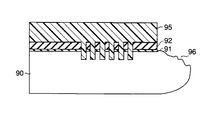
針状突起94の除去は、従来より、CDE(Chemical Dry Etching)法により行われている。まず、Siウェハ90の表面、すなわちデバイス表面全体にレジスト95を塗布し、ベベル部およびエッジ部数mmの領域のレジストを除去する。図17に、この段階の断面図を示す。
【0009】
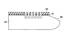
そして、CDE法を用いて、レジスト95で覆われていない部分のSiウェハ90を等方的にエッチングすることにより、ベベル部およびエッジ部の針状突起94を除去する(図18)。その後、デバイス表面を保護していたレジスト95を剥離する(図19)。
【0010】
CDE法では、デバイス表面をレジスト95で保護する必要があるため、レジスト塗布、レジスト剥離という工程が必要となる。また、等方的なエッチングのため、“針”は消滅するが、最初の“針”の高さばらつきに対応する凹凸96が残るため(図18、図19)、表面荒れを除去することは非常に困難である。
【0011】
この種の凹凸96は、次工程以降で行われるCMP等の加工時にダストが溜まり易く、問題になる場合があった。さらに、CDEに要する1枚当たりの処理時間は、通常5分以上と長く、スループットを下げ、原料コストが高くなると言う問題もある。
【0012】
ところで、近年、半導体装置の分野には、配線材料としてのCu、あるいは次世代DRAMやFeRAMのキャパシタ電極材料としてのRuやPt、キャパシタ誘電体材料としてのTaO、PZTなど、新材料が次々と導入されている。そして、量産化に当たり、これらの新材料による装置汚染の問題を真剣に考えるべき時期となった。
【0013】
特に、半導体装置製造工程中においてウェハのベベル部、エッジ部および裏面に付着し汚染源となる新材料膜の除去は、重要な課題である。例えば、キャパシタ電極として用いるRu膜を成膜する際、ベベル部、エッジ部および裏面に付着するRu膜の除去である。
【0014】
このようなRu膜の成膜方法として、現在一般に用いられるのがCVD法である。この場合、装置構成による程度の差こそあれ、ベベル部、エッジ部および裏面へのRu膜の付着は不可避である。
【0015】
また、スパッタ法においてエッジカットリングを用いた場合でも、ベベル部およびエッジ部へのスパッタ粒子(Ru)回り込みによるRu膜の付着をなくすのは困難である。外周チップの歩留りの関係上、エッジカット幅を小さくする場合は、なおさらである。
【0016】
いずれの成膜方法にせよ、Ru成膜後のウェハのベベル部、エッジ部あるいは裏面には、Ru膜が付着している。この種のベベル部等に付着したRu膜は、次工程の装置汚染の原因になるため、除去しなければならない。
【0017】
ベベル部等に付着したRu膜の除去は、従来より、ウェットエッチング法により行われている。Siウェハの裏面を上にして水平に回転しているSiウェハに薬液を滴下する方式が一般的である。ベベル部およびエッジ部に関しては、回転数等を調整して、薬液のデバイス面側への回り込み量を調整することにより対処している。
【0018】
しかし、Ru膜の場合、除去レートが10nm/min程度であるため、1枚当たりの除去時間が通常5分以上と長く、スループットが低いという問題があった。さらに、下地に拡散したRuを除去することができず、これを除去するには下地をエッチングできる別の薬液によるウェットエッチングを付加する必要がある。これはスループットをさらに低くすることになる。また、装置ダメージを与えない適当な薬液が存在しないという問題もある。
【0019】
【発明が解決しようとする課題】
上述の如く、トレンチの形成時に、ウェハのベベル部およびエッジ部にパーティクルの原因となる針状突起が発生する。従来技術では、この種の表面荒れの除去をCDE法により行っている。しかし、“針”は消滅するが、最初の“針”の高さばらつきに対応する凹凸が残るため、表面荒れを除去することが非常に困難であるという問題があった。
【0020】
また、キャパシタ電極としてのRu膜の形成時に、ウェハのベベル部、エッジ部および裏面に汚染原因となるRu膜が付着する。従来技術では、この種の付着膜をウエットエッチングにより行っている。しかし、除去レートが遅く、付着膜の除去に時間がかかるという問題があった。
【0021】
本発明は、上記事情を考慮してなされたもので、その目的とするところは、半導体装置の製造中において、基板の周縁部、裏面上の不要なものを効果的に除去できる半導体装置の製造方法および研磨装置を提供することにある。
【0022】
【課題を解決するための手段】
本願発明において開示される発明のうち、代表的なものの概要を簡単に説明すれば下記の通りである。すなわち、上記目的を達成するために、本発明に係る半導体装置の製造方法は、少なくとも基板の上面に半導体素子を形成する工程と、
少なくとも前記半導体素子の一部が形成された状態で前記基板の周縁部を研磨する工程とを有し、
前記基板の周縁部を研磨する工程は、
前記基板の周縁部に研磨面が接触するように研磨フィルムを配置し、
前記基板の上面と底面とに対して夫々所定の角度で前記研磨フィルムを前記基板の周縁部に押し付けるために、溝型の部品にその両端部が取り付けられた弾性体フィルムを用いて、前記基板の周縁部を前記研磨フィルムと前記弾性体フィルムとともに前記溝型の部品の溝内に押し込み、このときに引き伸ばされた弾性体フィルムを前記基板の周縁部に前記研磨フィルムを介して押し付けて前記弾性体フィルムと前記基板の周縁部との間に前記研磨フィルムが挟持されるように前記弾性体フィルムおよび溝型の部品を配置し、
前記引き伸ばされた弾性体フィルムが前記研磨フィルムを介して前記基板の周縁部に押し付けられたときに前記弾性体フィルムに張力が発生されることを特徴とする。前記基板の周辺部は、例えば、ベベル部およびエッジ部、またはベベル部のみである。
【0023】
また、本発明に係る研磨装置は、基板の周縁部に接触するように配置される研磨面を有する研磨フィルムと、
両端部を有し、この両端部の間で前記基板の上面と底面とに対して夫々所定の角度で前記研磨フィルムを前記基板の周縁部に押し付けるように配置される弾性体フィルムと、
前記弾性体フィルムの両端部が取り付けられる溝型の部品からなり、
前記基板の周縁部が前記研磨フィルムと弾性体フィルムとともに前記溝型の部品における溝内に押し込まれたときに前記基板の周縁部と前記溝の内側面との間に前記研磨フィルムと弾性体フィルムとが挟持されるように配置される押し付け部材と、
を具備し、前記基板の周縁部が前記研磨フィルムと弾性体フィルムとともに前記押し付け部材の溝内に押し込まれたときに前記弾性体フィルムに張力が発生して前記研磨フィルムに押し付けられることを特徴とする。
【0025】
本発明に係る半導体装置の製造方法によれば、半導体装置の製造中において、
基板の周縁部、裏面を研磨することによって、基板の周縁部、裏面上の不要なものを十分に除去できたり、短時間で除去できるようになる。
【0026】
上記研磨は、本発明に係る研磨装置により実施することが望ましい。その理由は、本発明に係る研磨装置によれば、張力を有する押し付け部材を用いて研磨手段を基板に押しつけることによって、研磨手段と基板との接触面積を大きくできるとともに、研磨手段と基板との接触面における圧力のばらつきを改善でき、研磨手段と基板との密着性を改善できるからである。
【0027】
本発明に係る半導体装置の製造方法、研磨装置のより具体的な形態は以下の通りである。
【0028】
(1)研磨の方式は固定砥粒方式である。
【0029】
(2)上記固定砥粒方式は、砥粒をフィルム上に接着剤で結合させた研磨フィルムを用いたものである。
【0030】
(3)上記研磨フィルムは、基板との接触部が研磨により摩耗する前に、研磨していない箇所が接触するように送り出される巻き取り式である。
【0031】
(4)上記研磨フィルムは、基板の周縁部および裏面の一方に対し、張力を有する部材によって押しつけられる。
【0032】
(5)上記研磨フィルムは、該研磨フィルムの裏面から基板の周縁部の曲率および基板の円周の曲率に沿うように変形可能な弾性体により基板に押し当てられ、上記研磨フィルムが基板の周縁部の曲率および基板の円周の曲率に沿うように接触される。
【0033】
(6)上記弾性体の形状は、フィルム状である。
【0034】
(7)上記弾性体は、薄い弾性体からなる袋に流体を入れて密閉したクッションである。
【0035】
(8)上記研磨フィルムのフィルムは、弾性体により形成されている。
【0036】
(9)上記研磨フィルムは、テープ状の形態をしており、該テープの長手方向が基板の表面に対して斜めになるように該基板の周縁部に接触する。
【0037】
(10)上記固定砥粒方式は、薄膜状の砥石を用いたものである。
【0038】
(11)上記固定砥粒方式は、砥粒を紐の表面に接着剤で結合させた研磨紐を用いたものである。
【0039】
(12)上記固定砥粒は、基板(表面に被研磨膜が形成されたものを含む)に対し、メカノケミカル研磨作用を有する。
【0040】
(13)上記研磨の方式は乾式である。
【0041】
(14)研磨の最中に基板上に気流を吹き付ける工程(手段)を有し、研磨屑を基板から排除する。
【0042】
(15)研磨の最中に前記基板上に液体を流す工程(手段)を有し、研磨屑を基板から排除する。
【0043】
(16)研磨時に研磨状態をモニターして研磨動作を制御する工程(手段)を有する。
【0044】
(17)上記モニターは、上記基板の被研磨部表面の凹凸度合いに基づいて行うものであって、例えば基板に光を照射する工程(手段)と、該光の散乱光を検出する工程(手段)と、検出結果に基づいて凹凸度合いを求める工程(手段)により行う。
【0045】
(18)上記モニターは、基板の周縁部および裏面の少なくとも一方に付着する膜(付着膜)の膜厚に基づいて行うものであって、例えば付着膜の膜厚を該付着膜の電気抵抗を測定する工程(手段)と、測定結果に基づいて膜厚を求める工程(手段)により行う。
【0046】
本発明の上記ならびにその他の目的と新規な特徴は、本明細書の記載および添付図面によって明らかになるであろう。
【0047】
【発明の実施の形態】
以下、図面を参照しながら本発明の実施の形態(以下、実施形態という)を説明する。
【0048】
(第1の実施形態)
本実施形態では、トレンチキャパシタのトレンチを、Siウェハ表面にRIE法により形成したときに、Siウェハのベベル部およびエッジ部に発生した表面荒れを除去する方法について説明する。上記トレンチキャパシタは、例えばDRAMのメモリセルに使用するものである。
【0049】
まず、図15および図16に示した従来の工程に従い、Siウェハ90上にハードマスク91、92を形成した後、このマスクを用いてトレンチ93を形成する。ここでは、ハードマスクのシリコン窒化膜91の厚さは200nm、SiO2 膜92の厚さは900nmとし、トレンチ93の開口径を0.25μm、深さを7μmとする。
【0050】
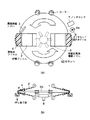
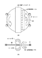
次に、図16のRIE工程で発生した針状突起94の除去工程に進む。本実施形態では、図1に示す研磨装置を用いて針状突起94の除去を行う。図1(a)はSiウェハをセットした状態を真上から見た概略図、図1(b)は真横から見た概略図である。
【0051】
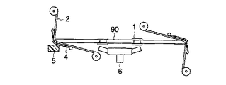
Siウェハ90は、上から落下するパーティクル対策のため、デバイス面が下になるようにセットされており、ローラー1により挟まれ、水平面内で回転できるようになっている。そして、研磨フィルム2が、Siウェハ90のベベル部の表面(ベベル面)に沿って接触するように張られている。ベベル面と研磨フィルム2の接触部には、薬液あるいは純水が薬液供給ノズル3から供給されれる。その量は、上記接触部が湿る程度である。このようにして、ベベル面はSiウェハ90を回転させることにより湿式研磨される。ここでは、簡単のため、2つの研磨フィルム2しか示していないが、実際にはより多くの数(例えば後述するように8)の研磨フィルム2が使用される。ただし、同時に使用されるのは4つである。
【0052】
研磨フィルム2の裏側からは、弾性ゴム等からなる弾性体フィルム4を押し当て、ウェハ円周に沿って研磨フィルム2が接触するようにする。弾性体フィルム4は引っ張れた状態で使用され、張力を有する。
【0053】
もし、弾性体フィルム4がないと、研磨フィルム2は、ウェハ円周に対して、
その中央部でしか接触することができず、接触長さは高々10mm程度になってしまい、接触面積を大きくできない。
【0054】
さらに、研磨フィルム2とSiウェハ90との接触面における圧力のばらつきを改善でき、接触面における研磨量のばらつきを十分に小さくできるようになる。この接触面における研磨量のばらつき低減の効果は、弾性体を単に押しつけるだけでは得られず、張力を有する状態で押しつける必要がある。
【0055】
このように研磨に寄与する部分を拡張して研磨レートを大きくするとともに、
接触面における圧力のばらつきを低減して研磨量を一様にするためには、張力を有する弾性体フィルム4は非常に重要である。
【0056】
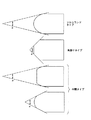
ベベル形状には、大別すると、図20に示すように、フルラウンドタイプと、
角張りタイプと、これらの中間タイプとがある。研磨フィルム2がベベル面全体に接触するように、図1(b)に示す角度θ(Siウェハ90と弾性体フィルムとのなす角度の2倍)は、図20に示す角度α(ベベル部とエッジ部の境界点における、ベベル部に対する両接線が成す角度)以下に設定する。
【0057】
研磨フィルム2とSiウェハ90との接触面における圧力の大きさは、弾性体フィルム4に作用する張力をT、弾性体フィルム4の幅をw、ベベル断面の曲率半径をρとすると、T/(ρw)となる。ただし、研磨フィルム2の厚さは、曲率半径ρに比し、十分小さいとする。よって、曲率半径ρがベベル断面全体に渡りほぼ一定なフルラウンドタイプでは、上記接触面における圧力のばらつきが小さいことがわかる。
【0058】
一方、ベベル断面に直線的部分を有する角張りタイプでは、直線的部分の曲率半径が大きいため、直線的部分での圧力が小さくなり、圧力のばらつきが発生する。
【0059】
この圧力ばらつきを改善するためには、直線的部分に平行な剛体面が弾性体フィルム4の裏面(研磨フィルム2と接触する面を表面とする。)から押し当たるようにすればよい。
【0060】
具体的には、図21に示すような工夫が考えられる。溝型の剛体51に弾性体フィルム4を取り付けた部品52を用意する(図21(a))。
【0061】
Siウェハ90のベベルに向かって、部品52を水平方向に押し込み、角度θが所定の値になるまで弾性体フィルム4を引き伸ばす。この時、溝型の剛体51の内側面に弾性体フィルム4が接触するようにする。ベベル断面の直線的部分に対応する弾性体フィルム4の裏面が、溝型の剛体51の内側面に密着して接触するように、溝型の剛体51の内側面を形成する。この接触による弾性体フィルム4の圧縮応力が、ベベル断面の直線的部分に付加される圧力として作用することになる(図21(b))。
【0062】
この圧縮応力が所望の研磨荷重になるように、溝型の剛体51の内側面を具体的に決定する方法を以下に述べる。
【0063】
まず、弾性体フィルム4を、溝型の剛体52の内側面に接触させることなく、
角度θが所定の値になるまで引き伸ばす。この状態で、溝型の剛体52の仮想的な内側面を、弾性体フィルム4の裏面の直線的部分に沿うように、直線で囲って決める(図21(c)の点線)。
【0064】
この仮想的な内側面から法線方向に後述する距離dだけ弾性体フィルム4側に移動させた面が、溝型の剛体52の実際の内側面である(図21(d)の実線)。距離dは、弾性体フィルム4の厚さをD、ヤング率をEとすると、E・(d/D)=研磨荷重の関係を満足する。厚さD、ヤング率E、必要とする弾性体フィルム4の圧縮応力(上記所望の研磨荷重)は予め分かっているので、これらの値を上式に代入することにより、距離dは求まる。
【0065】
ベベル形状が中間タイプの場合も、同様にして、直線的部分に平行な剛体面が弾性体フィルム4の裏面から押し当たるようにすればよい(図21(e)、図21(f))。
【0066】
このように、研磨フィルム2のベベル面への接触の強さは、フルラウンドタイプの場合は、弾性体フィルム4の張力Tで、また、角張りタイプと中間タイプの場合は、弾性体フィルム4の張力Tと上述した距離dで調整する。
【0067】
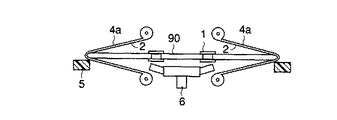
それから、ベベル部とは別に、デバイス面のエッジ部数mmの領域を研磨するために、弾性体からなる押し当て板5の水平面を鉛直方向から押し当て、研磨フィルム2がエッジ部領域に圧力換算で98066.5Pa(=1kg重/cm2 )程度に接触するように調整する。
【0068】
研磨フィルム2は、巻き取り式になっており、Siウェハ90との接触部が摩耗して研磨レートが低下する前に、新しい研磨フィルム部位が接触するように順送りするようになっている。
【0069】
また、研磨時に発生する研磨屑がSiウェハ90のデバイス面を汚すことを防ぐ目的で、放射状気体噴射ノズル6から空気あるいは窒素等の気体をデバイス面上に吹き付けられるようになっている。デバイス面の中心から放射線状に、流速5m/sec以上の気流をデバイス面に対して浅い角度で入射させる。放射状気体噴射ノズル6は、デバイス面側のみならず、Siウェハ90の裏面側にも設置すれば、より効果的である。
【0070】
Siウェハ90のノッチ(不図示)の研磨は、ノッチセンサ7によりノッチの位置合わせをして、Siウェハ90の回転を止め、ノッチおよびベベルの形状に合った図2(a)に示すような#10000程度のダイヤモンド砥石ホイール8により行う。図2(b)は、ダイヤモンド砥石ホイール8をノッチに当てた状態を真上から見た透視図である。ダイヤモンド砥石ホイール8の側面の凹みをノッチのベベル部に合わせ、回転軸8aを左右、上下に動かして、ノッチのベベル部およびエッジ部の全体を研磨する。
【0071】
このような構成の研磨装置において、以下の条件によりベベル部およびエッジ部の研磨を行った。
【0072】
【0073】
次に、粗削り用の研磨フィルム2aを仕上げ用の研磨フィルム2bに切り替え、仕上げ用の研磨フィルム2bによる1分間の研磨を行う。この研磨(仕上げ研磨)により表面に残存する研磨ダメージは十分に除去され、ベベル面は平均粗さRaが数nm以下の鏡面になる。
【0074】
次に、ウェハノッチの研磨を行う。ダイヤモンド砥石ホイール8を1000rpmで回転させて30秒間研磨することにより、ノッチにおける針状突起は十分にに除去される。
【0075】
この後、別のユニットにおいて、ベベル部およびエッジ部を主体にSiウェハ90をPVAスポンジ等で擦り付けながら、純水あるいは界面活性剤水溶液を用いて洗浄し、リンスし、乾燥させることにより、ベベル部およびエッジ部の針状突起の研磨除去が終了する。
【0076】
このように、研磨フィルム2a,2bという固定砥粒を用いることにより、従来のCDE法では不可欠だった、レジストによるデバイス面の保護が不要になる。その結果、保護用のレジスト塗布、針状突起除去後のレジスト剥離という2工程を省けるようになる。
【0077】
また、研磨法によると、ベベル部およびエッジ部の針状突起の除去後の面は平滑面となる(図4)。よって、図18、図19に示した従来のCDE法では問題になった、針状突起の除去後に残存する、最初の“針”の高さばらつきに対応する凹凸96に、次工程以降で行われるCMP等の加工時にダストが溜まり易いという問題は解決される。
【0078】
また、洗浄部をユニットとして組み込んだ、本実施形態の研磨装置により針状突起の除去を行えば、ウェハ1枚当たりの処理時間を上述のように3分程度にすることが可能である。よって、従来のCDE法の5分以上に比べて、処理時間は短縮し、スループットは向上する。
【0079】
さらに、図5に示すように、本研磨装置を研磨フィルム2が連続するようにして縦に積み上げ、共通の軸でローラーを回す構造にすれば、同時に複数枚のSiウェハ90の研磨処理が可能になり、スループットはさらに向上する。
【0080】
さらに、本研磨装置は装置構成が簡単なため、装置単体の価格は安くなる。また、使用原料も純水と微量の薬液だけなので、ランニングコストを大幅に削減できる。このように本実施形態によれば、コスト削減の点で大きな利点がある。
【0081】
本研磨装置には、研磨中に研磨の状態をモニターし、結果を研磨動作にフィードバックさせるIn−situタイプのモニター機構を搭載することが可能である。
【0082】
モニター機構としては、例えばウェハに光を照射する光源と、該光の散乱光を検出する光検出器と、検出結果に基づいて研磨の終点を判定する判定部とで構成された、光学的手法を利用した機構があげられる。
【0083】
研磨初期はベベル面が荒れているため、ウェハに照射した光は乱反射し、反射強度は弱い。しかし、研磨が進行するにつれ、ベベル面は鏡面反射へと移行していき反射強度は強まる。判定部は、光検出器で検出された光の強度(反射強度)と予め決められたあるレベル(しきい値)とを比較し、反射強度がしきい値以上となった時点を研磨の終点として判定する。
【0084】
本研磨装置の構成は、本発明の趣旨を逸脱しない範囲で、変化させることが可能である。特に、研磨フィルム2のウェハ円周に対する接触のさせ方は、いろいろな変形が考えられる。
【0085】
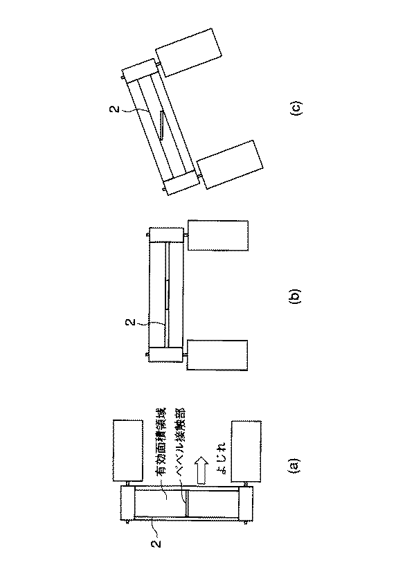
本実施形態では、研磨フィルム2は、その長手方向がウェハ面に直交するように配置されている(図6(a))。この配置の場合、研磨フィルム2がウェハの回転方向に引きずられ、よじれる可能性がある。また、研磨フィルム2の巻き取りの回転軸がウェハ回転軸と直交するため、研磨フィルム2の巻き取り駆動部がウェハ回転駆動部に対し、コンパクトに収まりにくい。
【0086】
これらの点を改善するために、研磨フィルム2の長手方向がウェハ面に平行になるように配置する方法もある(図6(b))。この配置の場合、研磨フィルム2の有効面積が極端に小さくなり、高価な研磨フィルムを用いる場合は、非経済的である。
【0087】
そこで、図6(c)に示すように、研磨フィルム2の長手方向がウェハ面に対して斜めになるようにする方法が考えられる。このようにすれば、研磨フィルム2はよじれにくくなり、かつ、有効面積を大きくすることが可能になる。
【0088】
張力を有する部材を利用した、研磨フィルム2のベベル部およびエッジ部への荷重印加に関しても、別の方法が考えられる。例えば、図7に示すように、研磨フィルム2と引き伸ばした弾性体フィルム4aを重ね合わせて両者を同時に巻き取っていく構成もある。また、研磨フィルム2のフィルムの材質そのものを弾性ゴムのような弾性体にする構成もある。
【0089】
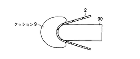
また、弾性体フィルム4を用いる構成の代わりに、図8に示すように、クッション9を研磨フィルム2に当てる構成にしても良い。クッション9は、外側が薄い弾性体膜からなる袋の中に空気などの気体もしくは水などの流体を満たし密閉したもので、パスカルの原理に基づき、ベベル面に均等な圧力をかける効果を期待できる。
【0090】
また、本実施形態のような、1つの研磨フィルム2でウェハ両面側のベベル面に接触させる構成ではなく、例えば図9に示すように、片面側ずつ接触させる構成もある。この構成の方がベベル面の曲率に確実に沿わせられる。
【0091】
さらに、このようなベベル面に片面側ずつ接触させる構成では、研磨フィルム2の曲げが少なくなるので、曲がりにくい厚めの研磨フィルムを用いることも可能になる。研磨フィルム2の代わりに薄膜状の砥石を用いることも可能になる。
【0092】
また、ウェハの回転をローラー1を用いて行ったが、ウェハ裏面を真空吸着チャックし回転駆動させても良い。
【0093】
また、研磨のプロセス条件も、適宜、変更可能である。研磨フィルムの形態、砥粒の種類も、限定されるものではない。例えば、砥粒にBaCO3 等のシリコンに対してメカノケミカル作用を有する材料を使用することもできる。
【0094】
また、湿式研磨の供給液体としては、純水以外に、シリコンをウェットエッチングする薬液、例えばKOH水溶液、アルカリイオン水等も使用可能である。また、界面活性剤水溶液も使用可能である。これらの薬液の使用により、研磨フィルム2の砥粒の材質とサイズによっては、研磨レートあるいは表面平坦度といった研磨特性が向上する効果が期待できる。
【0095】
また、研磨屑排除の目的で、デバイス面上に気体を吹き付ける方式を用いているが、デバイス面上に純水等の液体を流すことも可能である。
【0096】
(第2の実施形態)
図10は、本発明の第2の実施形態に係る研磨装置を示す概略図である。これはSiウェハ90をセットした状態を真上から見た概略図である。なお、図1と対応する部分には図1と同一符号を付してあり、詳細な説明は省略する。
【0097】
本研磨装置が第1の実施形態で説明した研磨装置と異なる点は、研磨フィルムの代わりに紐状の研磨体、すなわち、研磨紐20を用いることである。研磨紐20は、PET、ポリエステル等の高分子樹脂からなる紐の表面に、砥粒を接着剤で結合させたものである。なるべく多くの本数の研磨紐20をウェハ円周に沿って接触するように配置することにより、研磨レートの向上を効果的に図れる。
【0098】
この方式では、研磨フィルム方式では必要であった、接触部をウェハ円周に沿わせるための弾性体フィルム等は、不要になる利点がある。研磨紐20の断面を長方形にして、長辺側をウェハ円周に接触させることが、接触距離が長くなるため、研磨レート向上の観点から好ましい。
【0099】
(第3の実施形態)
図11は、本発明の第3の実施形態に係る研磨装置を示す概略図である。図11(a)はウェハをセットした状態を真上から見た概略図、図11(b)は真横から見た概略図である。なお、図1と対応する部分には図1と同一符号を付してあり、詳細な説明は省略する。
【0100】
本研磨装置が第1の実施形態と異なる点は、湿式研磨ではなく乾式研磨を行うという点である。乾式研磨では、一般に、研磨屑等のパーティクルが静電気的に付着し易い。そして、これらのパーティクルは飛散し、デバイス面を汚す危険がある。
【0101】
そこで、本実施形態では、研磨時に発生する研磨屑を排除する目的で、空気あるいは窒素等の気体を吹き付ける気体噴射ノズルを設ける。具体的には、デバイス面側へ飛散するパーティクルに対しては、Siウェハ90の下方に放射状気体噴射ノズル30を設ける。
【0102】
放射状気体噴射ノズル30は、デバイス面の中心から放射線状に、デバイス面に対して浅い角度で入射するように、流速5m/sec以上の気流をデバイス面に吹き付ける。これにより、研磨屑を効果的に排除することが可能となる。放射状気体噴射ノズル30は、デバイス面側のみならず、ウェハ裏面側にも設置すれば、より効果的である。
【0103】
さらに、研磨直後、静電気的にベベル面に付着したパーティクルは、接線方向気体噴射ノズル31から吹き付ける気流により排除する。具体的には、研磨フィルム2に擦られて出てきた直後のウェハ外周に対して、ウェハ外周接線に沿ってウェハ回転方向に流速10m/sec以上の気流を吹き付けるようにする。
【0104】
乾式研磨を用いると、純水を節約でき、廃液処理が不要になる。また、メカノケミカル作用という固相反応を積極的に利用する研磨の場合、乾式の方が湿式より研磨レートが速いことが一般に知られている。よって、シリコンに対してメカノケミカル作用を有するBaCO3 等の砥粒を研磨フィルム2に使用する際、本実施形態の乾式研磨は有効な手法となる。
【0105】
(第4の実施形態)
本実施形態では、スタックキャパシタのキャパシタ電極(下部電極)として用いるRu膜をデバイス面上にCVD法で成膜した際、Siウェハのベベル部、エッジ部および裏面に付着し、汚染源となるRu膜の研磨法による除去について説明する。
【0106】
図12に示すように、シリコン窒化膜97を成膜したSiウェハ90上に、下部キャパシタ電極として用いるRu膜98をバッチ式のCVD法により30nmだけ成膜した場合、Ru膜98はデバイス面のみならず、ウェハのベベル部、エッジ部および裏面にも30nm程度成膜される。この種のRu膜98を用いるキャパシタは、例えば、シリンダ型、クラウン型などのよく知られた三次元構造の立体キャパシタである。この立体キャパシタは、例えばDRAMまたはFeRAMに使用されるものである。
【0107】
ベベル部、エッジ部および裏面に付着したRu膜98は、次工程の装置汚染をもたらす関係上、除去することが必要になる。ベベル部およびエッジ部のRu膜98の除去を第1の実施形態で説明した図1の研磨装置により行った。研磨条件は以下の通りである。
【0108】
【0109】
次に、ウェハノッチ(不図示)のベベル部およびエッジ部に付着しているRu膜98の除去を、第1の実施形態と同様に、ダイヤモンド砥石ホイール8により行う。同ホイール8を1000rpmで回転させて30秒研磨することにより、上記部分のRu膜98を除去することができた。
【0110】
裏面に付着したRu膜98は、図13に示す研磨装置により除去する。図13(a)はウェハをセットした状態を真上から見た概略図、図13(b)は真横から見た概略図である。
【0111】
Siウェハ90は、デバイス面が下になるようにセットされており、ローラー41により挟まれ、水平面内で回転できるようになっている。そして、シャワーノズルの形態をした薬液供給ノズル42から、薬液がウェハ裏面に滴下される。そこへ、研磨フィルムを弾性体に巻き付けた研磨フィルムロール43が、Siウェハ90の裏面に回転しながら接触し、ウェハ裏面は湿式研磨される。
【0112】
研磨フィルムロール43は、円柱状の弾性ゴム、発砲ウレタン等に研磨フィルムを接着して巻き付けたもので、サイズは、20.32cm(8インチ)ウェハ用としては、直径30mm程度、長さ210mm程度である。
【0113】
また、PVAスポンジからなるロール44が、洗浄液供給ノズル45から供給される洗浄液を介して、Siウェハのデバイス面に回転しながら接触できるようになっている。ロール44の役割は、研磨フィルムロール43の荷重を支えることである。
【0114】
このような研磨装置において、以下の条件により研磨を行った。
【0115】
研磨フィルム:粒度#10000番のダイヤモンドがPETフィルム上にウレタンタイプ接着剤で結合されたもの
研磨フィルムロール押し付け力:1kg重
研磨フィルムロール回転数:100rpm
ウェハ回転数:100rpm
薬液:純水(200ml/min供給)
洗浄液:純水(1000ml/min供給)
2分間の研磨により、裏面のRu膜98も除去された(図14)。
【0116】
この後、別のユニットにおいて、ベベル面も含めウェハ全体をPVAスポンジ等で擦り付けながら、純水あるいは界面活性剤水溶液を用いて洗浄し、リンスし、乾燥させることにより、ベベル部、エッジ部および裏面のRu膜の研磨除去が終了する。
【0117】
Ru膜98が除去されて露出した下地のシリコン窒化膜97上は、ICP分析によるRu汚染が1010atoms/cm2 未満になるまで清浄化されることが確認された。
【0118】
従来のウェットエッチング法では、例えば、薬液に硝酸二アンモニウムセリウム20%水溶液を用いた場合、Ru汚染を1011atoms/cm2 未満にするのでさえ5分以上かかり、1010atoms/cm2 未満にするためには、下地のシリコン窒化膜97を希フッ酸等の別の薬液で2分間程度ウェットエッチングする必要があった。よって、従来法では、ベベル部、エッジ部および裏面のRu膜を除去するのに、1枚当たり、7分以上の時間を要していた。
【0119】
一方、本実施形態の研磨による除去方法では、ベベル部+エッジ部と裏面を分けて行う場合でも、3.5分である。ベベル部+エッジ部用装置(図1)と裏面用装置(図13)は、お互いに干渉しない形で一体化することも可能である。
【0120】
一体化した場合、ベベル部+エッジ部と裏面のRu膜研磨除去を同時に行うことが可能である。これにより、処理時間はさらに短縮され、2.5分になる。よって、大幅なスループット向上につながる。
【0121】
また、本実施形態の研磨法を実施する研磨装置は構成が簡単なため、装置単体の価格が安くなり、また、使用原料も純水と微量の薬液だけなので、ランニングコストも大幅に削減できる。
【0122】
本研磨装置には、研磨中に研磨の状態をモニターし、結果を研磨動作にフィードバックさせる、In−situモニター機構を搭載することが可能である。モニター機構としては、例えばRu膜の膜厚変化に伴う電気抵抗変化を測定する機構のものが好適である。
【0123】
同機構は、例えば回転しているウェハに擦れてもウェハを傷付けない導電性樹脂等からなる端子(2個)と、端子間に電圧を印加するための電圧源と、端子間に流れる電流、すなわちRu膜中を流れる電流を測定(モニター)する電流測定とで構成されたものである。
【0124】
研磨が進行するにつれ、Ru膜の膜厚は薄くなり電気抵抗が上昇するため、電流値は小さくなる。そして、Ru膜が除去され下地のシリコン窒化膜等の絶縁膜が露出した段階で、電流値はゼロになる。この時間に、下地に拡散したRu成分も削り取る時間も加味して終点を決定する。
【0125】
ベベル部のRu膜の研磨モニターに関しては、端子がベベル部に接触するように、裏面のRu膜の研磨モニターに関しては、端子が裏面に接触するように、端子形状あるいは端子位置をそれぞれ設定する。運動している面への接触なので、接触が離れないように、端子をバネ等で押すあるいは端子そのものを弾性体にすることが望ましい。
【0126】
印加する電圧は、ウェハ上のデバイスへの影響を考慮すると、なるべく小さい方が良く、mV以下オーダーの電圧が好ましい。また、直流ではなく、交流あるいは高周波の方が、電流波形の増幅、平滑化等の処理がしやすい利点がある。
【0127】
本実施形態の研磨装置の構成は、発明の趣旨を逸脱しない範囲で、変化させることが可能である。研磨のプロセス条件も、適宜、変更可能である。研磨フィルムの形態、砥粒の種類も、限定されるものではない。
【0128】
また、湿式研磨の供給液体としては、純水以外に、Ru膜をウェットエッチングする薬液、例えば硝酸二アンモニウムセリウム水溶液、過硫酸アンモニウム水溶液等の酸化剤も使用可能である。これらの薬液の使用により、研磨レートが向上する効果が期待できる。
【0129】
研磨法による汚染膜除去の特長は、砥粒のメカニカルな除去作用が加わることである。したがって、化学的に安定な膜の除去に対しても有効であり、また、下地に拡散した上記化学的に安定な膜の成分も、下地の一部を削り取ることにより除去することが可能である。この理由により、本研磨法により除去できる汚染膜は、Ru膜に限らず、Cu膜、PZT膜、BST膜等、今後、半導体装置の製造に導入される新材料膜一般に広げることができる。
【0130】
また、本実施形態では、素子の一部としてスタックキャパシタの下部電極を例にあげたが、プラグもしくは配線、またはこれらの3つうちの2つ以上でも構わない。
【0131】
なお、本発明は、上記実施形態に限定されるものではない。例えば、上記実施形態では、基板としてSiウェハを用いた場合について説明したが、SOIウェハを用いても良い。さらに、SiGeウェハ等の他の半導体ウエハ、あるいはデバイス面がSiGeで形成されたSiウェハを用いても良い。また、ベベル部のみ、または基板の裏面のみを研磨対象としても良い。
【0132】
また、上記実施形態には種々の段階の発明が含まれており、開示される複数の構成要件における適宜な組み合わせにより種々の発明が抽出され得る。例えば、実施形態に示される全構成要件から幾つかの構成要件が削除されても、発明が解決しようとする課題の欄で述べた課題を解決できる場合には、この構成要件が削除された構成が発明として抽出され得る。その他、本発明の要旨を逸脱しない範囲で、種々変形して実施できる。
【0133】
【発明の効果】
以上詳説したように本発明によれば、半導体装置の製造中において、基板の周縁部、裏面上の不要なものを効果的に除去できる半導体装置の製造方法および研磨装置を実現できるようになる。
【図面の簡単な説明】
【図1】本発明の第1の実施形態に係る研磨装置を示す概略図
【図2】Siウェハのノッチの研磨を説明するための図
【図3】本発明の第1の実施形態に係る粗削り研磨および仕上げ研磨に用いた研磨装置を示す概略図
【図4】本発明の第1の実施形態に係る研磨を行ったベベル部およびエッジ部の表面形状を示す断面図
【図5】本発明の第1の実施形態に係る研磨装置の変形例を示す概略図
【図6】本発明の第1の実施形態に係る研磨装置の研磨フィルムの配置例を示す図
【図7】本発明の第1の実施形態に係る研磨装置において張力を有する部材を利用して研磨フィルムをベベル部およびエッジ部に押しつける方法を説明するための図
【図8】本発明の第1の実施形態に係る研磨装置において変形可能な弾性体からなる押し付け部材を利用して研磨フィルムをベベル部およびエッジ部に押しつける他の方法を説明するための図
【図9】本発明の第1の実施形態に係る研磨装置において研磨フィルムをSiウェハの片面側ずつ接触させる構成を示す図
【図10】本発明の第2の実施形態に係る研磨装置を示す概略図
【図11】本発明の第3の実施形態に係る研磨装置を示す概略図
【図12】Ru膜を成膜したSiウェハを示す断面図
【図13】本発明の第4の実施形態に係る研磨装置を示す概略図
【図14】同研磨装置を用いて研磨したSiウェハの表面形状を示す断面図
【図15】トレンチの形成方法を説明するための断面図
【図16】図15に続くトレンチの形成方法を説明するための断面図
【図17】従来のトレンチの形成時に発生した針状突起の除去方法を説明するための断面図
【図18】図17に続く同針状突起の除去方法を説明するための断面図
【図19】図18に続く同針状突起の除去方法を説明するための断面図
【図20】ベベル形状のタイプを説明するための断面図
【図21】Siウェハのベベルに直線的部分がある場合に、研磨フィルムとSiウェハとの接触面における圧力のばらつきを改善する方法を説明するための断面図
【符号の説明】
1…ローラー
2,2a,2b…研磨フィルム
3…薬液供給ノズル
4、4a…弾性体フィルム
5…押し当て板
6…放射状気体噴射ノズル
7…ノッチセンサ
8…ダイヤモンド砥石ホイール
8a…回転軸
9…クッション
20…研磨紐
30…放射状気体噴射ノズル
31…接線方向気体噴射ノズル
41…ローラー
42…薬液供給ノズル
43…研磨フィルムロール
44…ロール
45…洗浄液供給ノズル
51…溝型の剛体
52…部品
90…Siウェハ
91…シリコン窒化膜
92…SiO2 膜
93…トレンチ
94…針状突起
95…レジスト
96…凹凸
97…シリコン窒化膜
98…Ru膜[0001]
BACKGROUND OF THE INVENTION
The present invention relates to a method of manufacturing a semiconductor device and a polishing apparatus, and more particularly to a method of manufacturing a semiconductor device having a step of removing surface roughness of a substrate and an adhesion film on the substrate, and a polishing apparatus for performing the method.
[0002]
[Prior art]
In recent years, with the miniaturization of semiconductor elements and the high integration of semiconductor devices, particle management is becoming increasingly important. One of the major problems in managing particles is dust generation from surface roughness caused by processing that occurs at the bevel and edge portions of the wafer (substrate) during the manufacturing process of the semiconductor device.
[0003]
Here, in this specification, a convex portion where the flatness of the wafer changes at the wafer end, such as a portion having a curvature at the wafer end or a portion having a square cross section, is called a bevel portion, and the bevel portion extends from the bevel portion to the inside of the wafer. A portion having a flat surface of about several millimeters facing is called an edge portion.
[0004]
Such surface roughness due to processing occurs, for example, in an RIE (Reactive Ion Etching) process in which the trench of the trench capacitor is formed on the surface of the Si wafer.
[0005]
That is, as shown in FIG. 15, a
[0006]
In particular, under the RIE process conditions for accurately forming the
[0007]
The needle-
[0008]
The removal of the
[0009]
Then, by using the CDE method, a portion of the
[0010]
In the CDE method, since it is necessary to protect the device surface with a
[0011]
This kind of
[0012]
By the way, in recent years, new materials such as Cu as a wiring material, Ru or Pt as a capacitor electrode material of next generation DRAM or FeRAM, TaO or PZT as a capacitor dielectric material are introduced one after another in the field of semiconductor devices. Has been. It was time to seriously consider the problem of equipment contamination caused by these new materials in mass production.
[0013]
In particular, removal of a new material film that adheres to the bevel portion, edge portion, and back surface of a wafer and becomes a contamination source during the semiconductor device manufacturing process is an important issue. For example, when a Ru film used as a capacitor electrode is formed, the Ru film attached to the bevel portion, the edge portion, and the back surface is removed.
[0014]
As a method for forming such a Ru film, the CVD method is generally used at present. In this case, it is inevitable that the Ru film adheres to the bevel portion, the edge portion, and the back surface, depending on the degree of the apparatus configuration.
[0015]
Further, even when an edge cut ring is used in the sputtering method, it is difficult to eliminate the adhesion of the Ru film due to the sputter particles (Ru) wrapping around the bevel portion and the edge portion. This is especially true when the edge cut width is reduced due to the yield of the peripheral chip.
[0016]
In any film forming method, a Ru film is adhered to the bevel portion, edge portion or back surface of the wafer after Ru film formation. The Ru film adhering to this type of bevel portion or the like causes contamination of the apparatus in the next process and must be removed.
[0017]
The Ru film adhering to the bevel portion and the like has been conventionally removed by a wet etching method. In general, a chemical solution is dropped onto a Si wafer that is rotating horizontally with the back surface of the Si wafer facing up. The bevel portion and the edge portion are dealt with by adjusting the number of rotations and the like, and adjusting the amount of the chemical liquid that wraps around the device surface.
[0018]
However, in the case of a Ru film, since the removal rate is about 10 nm / min, there is a problem that the removal time per sheet is usually as long as 5 minutes or more and the throughput is low. Further, Ru diffused in the base cannot be removed, and in order to remove this, it is necessary to add wet etching with another chemical solution capable of etching the base. This will further reduce the throughput. There is also a problem that there is no appropriate chemical that does not damage the device.
[0019]
[Problems to be solved by the invention]
As described above, when the trench is formed, acicular protrusions that cause particles are generated on the bevel portion and the edge portion of the wafer. In the prior art, this type of surface roughness removal is performed by the CDE method. However, although the “needle” disappears, the unevenness corresponding to the height variation of the first “needle” remains, so that there is a problem that it is very difficult to remove the surface roughness.
[0020]
Further, during the formation of the Ru film as the capacitor electrode, the Ru film that causes contamination adheres to the bevel portion, edge portion, and back surface of the wafer. In the prior art, this kind of adhesion film is performed by wet etching. However, there is a problem that the removal rate is slow and it takes time to remove the adhered film.
[0021]
The present invention has been made in consideration of the above circumstances, and the object of the present invention is to manufacture a semiconductor device capable of effectively removing unnecessary components on the peripheral edge and back surface of the substrate during the manufacture of the semiconductor device. It is to provide a method and a polishing apparatus.
[0022]
[Means for Solving the Problems]
Among the inventions disclosed in the present invention, the outline of typical ones will be briefly described as follows. That is, in order to achieve the above object, a method of manufacturing a semiconductor device according to the present invention includes a step of forming a semiconductor element on at least an upper surface of a substrate,
Polishing a peripheral edge of the substrate in a state where at least a part of the semiconductor element is formed,
The step of polishing the peripheral edge of the substrate includes
Polishing so that the polishing surface is in contact with the peripheral edge of the substrate the film And place
The polishing at a predetermined angle with respect to the top and bottom surfaces of the substrate, respectively. the film Press against the edge of the board For that, both ends were attached to the groove type parts Elastic body the film Using the peripheral edge of the substrate The Polishing The elastic film is pushed into the groove of the groove-shaped component together with the film and the elastic film, and the elastic film stretched at this time is pressed against the peripheral edge of the substrate via the polishing film, and the elastic film and the substrate Peripheral part Between the polishing Film To be pinched The elastic film and the groove-shaped component Place and
Said Stretched Elastic body Film Polishing the film The elastic body when pressed against the peripheral edge of the substrate via the film It is characterized in that tension is generated. The peripheral portion of the substrate is, for example, only a bevel portion and an edge portion, or a bevel portion.
[0023]
Further, the polishing apparatus according to the present invention is a polishing having a polishing surface arranged so as to contact the peripheral edge of the substrate. the film When,
Having both end portions, and polishing between the both end portions at a predetermined angle with respect to the top surface and the bottom surface of the substrate the film Elastic body arranged to press against the peripheral edge of the substrate the film When,
The elastic body the film Consisting of groove-shaped parts to which both ends of
The periphery of the substrate is the polished the film And elastic body the film And polishing between the peripheral edge of the substrate and the inner surface of the groove when pressed into the groove in the groove-shaped component. the film And elastic body the film And a pressing member arranged to be sandwiched between,
And the periphery of the substrate is the polished the film And elastic body the film Together with the elastic body when pushed into the groove of the pressing member the film The tension is generated in the polishing the film It is characterized by being pressed against.
[0025]
According to the method for manufacturing a semiconductor device according to the present invention, during the manufacture of the semiconductor device,
By polishing the peripheral edge and back surface of the substrate, unnecessary parts on the peripheral edge and back surface of the substrate can be sufficiently removed or can be removed in a short time.
[0026]
The polishing is preferably performed by the polishing apparatus according to the present invention. The reason is that according to the polishing apparatus of the present invention, the contact area between the polishing means and the substrate can be increased by pressing the polishing means against the substrate using a pressing member having tension, and the polishing means and the substrate This is because variation in pressure on the contact surface can be improved, and adhesion between the polishing means and the substrate can be improved.
[0027]
More specific embodiments of the semiconductor device manufacturing method and the polishing apparatus according to the present invention are as follows.
[0028]
(1) The polishing method is a fixed abrasive method.
[0029]
(2) The fixed abrasive method uses a polishing film in which abrasive particles are bonded on a film with an adhesive.
[0030]
(3) The polishing film is a take-up type in which a portion not polished is brought into contact before the contact portion with the substrate is worn by polishing.
[0031]
(4) The polishing film is pressed against one of the peripheral edge and the back surface of the substrate by a member having tension.
[0032]
(5) The polishing film is pressed against the substrate by a deformable elastic body along the curvature of the peripheral edge of the substrate and the curvature of the circumference of the substrate from the back surface of the polishing film, and the polishing film is Contact is made along the curvature of the part and the circumference of the substrate.
[0033]
(6) The shape of the elastic body is a film.
[0034]
(7) The elastic body is a cushion sealed by putting a fluid in a bag made of a thin elastic body.
[0035]
(8) The film of the polishing film is formed of an elastic body.
[0036]
(9) The polishing film has a tape-like form, and contacts the peripheral edge of the substrate so that the longitudinal direction of the tape is inclined with respect to the surface of the substrate.
[0037]
(10) The fixed abrasive grain method uses a thin-film-shaped grindstone.
[0038]
(11) The fixed abrasive method uses an abrasive string in which abrasive grains are bonded to the surface of the string with an adhesive.
[0039]
(12) The fixed abrasive has a mechanochemical polishing action on a substrate (including a substrate on which a film to be polished is formed).
[0040]
(13) The polishing method is dry.
[0041]
(14) A step (means) of blowing an airflow onto the substrate during polishing to remove polishing debris from the substrate.
[0042]
(15) A step (means) of flowing a liquid over the substrate during polishing, and removing polishing debris from the substrate.
[0043]
(16) A step (means) for controlling the polishing operation by monitoring the polishing state during polishing.
[0044]
(17) The monitor is based on the degree of unevenness of the surface of the substrate to be polished. For example, a step (means) of irradiating the substrate with light and a step (means) of detecting scattered light of the light ) And a step (means) for obtaining the degree of unevenness based on the detection result.
[0045]
(18) The monitor is based on the film thickness of the film (adhesion film) adhering to at least one of the peripheral edge and the back surface of the substrate. For example, the thickness of the adhesion film is set to the electric resistance of the adhesion film. It is performed by a step (means) for measuring and a step (means) for obtaining a film thickness based on the measurement result.
[0046]
The above and other objects and novel features of the present invention will become apparent from the description of the present specification and the accompanying drawings.
[0047]
DETAILED DESCRIPTION OF THE INVENTION
Hereinafter, embodiments of the present invention (hereinafter referred to as embodiments) will be described with reference to the drawings.
[0048]
(First embodiment)
In the present embodiment, a method for removing surface roughness generated at the bevel portion and the edge portion of the Si wafer when the trench of the trench capacitor is formed on the Si wafer surface by the RIE method will be described. The trench capacitor is used for a DRAM memory cell, for example.
[0049]
First, in accordance with the conventional process shown in FIGS. 15 and 16, after forming hard masks 91 and 92 on the
[0050]
Next, the process proceeds to a process of removing the needle-
[0051]
The
[0052]
From the back side of the polishing
[0053]
If the elastic film 4 is not present, the polishing
The contact can be made only at the center, and the contact length is about 10 mm at most, so that the contact area cannot be increased.
[0054]
Furthermore, the pressure variation at the contact surface between the polishing
[0055]
In this way, the portion that contributes to polishing is expanded to increase the polishing rate,
In order to reduce the variation in pressure on the contact surface and make the polishing amount uniform, the elastic film 4 having tension is very important.
[0056]
The bevel shape is roughly divided into a full round type as shown in FIG.
There are square type and intermediate type. The angle θ shown in FIG. 1B (twice the angle formed between the
[0057]
The magnitude of the pressure at the contact surface between the polishing
[0058]
On the other hand, in the square type having a straight portion in the bevel cross section, the curvature radius of the straight portion is large, so that the pressure in the straight portion is reduced, and the pressure varies.
[0059]
In order to improve the pressure variation, the rigid surface parallel to the linear portion may be pressed from the back surface of the elastic film 4 (the surface contacting the polishing
[0060]
Specifically, a device as shown in FIG. 21 can be considered. A
[0061]
The
[0062]
A method for specifically determining the inner surface of the groove-type
[0063]
First, without bringing the elastic film 4 into contact with the inner surface of the groove-shaped
Stretch until the angle θ reaches a predetermined value. In this state, the virtual inner surface of the groove-shaped
[0064]
It will be described later in the normal direction from this virtual inner surface. Only distance d The surface moved to the elastic film 4 side is the actual inner surface of the groove-shaped rigid body 52 (solid line in FIG. 21 (d)). The distance d satisfies the relationship of E · (d / D) = polishing load, where D is the thickness of the elastic film 4 and E is the Young's modulus. Since the thickness D, Young's modulus E, and the necessary compressive stress (the desired polishing load) of the elastic film 4 are known in advance, the distance d can be obtained by substituting these values into the above equation.
[0065]
Similarly, when the bevel shape is an intermediate type, the rigid surface parallel to the linear portion may be pressed from the back surface of the elastic film 4 (FIGS. 21E and 21F).
[0066]
Thus, the strength of contact of the polishing
[0067]
Then, separately from the bevel part, in order to polish the area of the edge part several mm of the device surface, the horizontal surface of the
[0068]
The polishing
[0069]
In addition, for the purpose of preventing polishing scraps generated during polishing from contaminating the device surface of the
[0070]
The notch (not shown) of the
[0071]
In the polishing apparatus having such a configuration, the bevel portion and the edge portion were polished under the following conditions.
[0072]
[0073]
Next, the polishing
[0074]
Next, the wafer notch is polished. By rotating the
[0075]
Thereafter, in another unit, the bevel portion is cleaned by rinsing, rinsing, and drying the pure wafer or the surfactant aqueous solution while rubbing the
[0076]
Thus, by using the fixed abrasive grains of the polishing
[0077]
Further, according to the polishing method, the surface after the removal of the needle-like protrusions at the bevel portion and the edge portion becomes a smooth surface (FIG. 4). Therefore, the
[0078]
Further, if the needle-like protrusions are removed by the polishing apparatus of this embodiment in which the cleaning unit is incorporated as a unit, the processing time per wafer can be reduced to about 3 minutes as described above. Therefore, the processing time is shortened and the throughput is improved as compared with the conventional CDE method of 5 minutes or more.
[0079]
Furthermore, as shown in FIG. 5, if the polishing apparatus is stacked vertically so that the polishing
[0080]
Furthermore, since the polishing apparatus has a simple apparatus configuration, the price of the apparatus alone is reduced. In addition, since the raw materials used are pure water and a small amount of chemical solution, running costs can be greatly reduced. Thus, according to this embodiment, there is a great advantage in terms of cost reduction.
[0081]
This polishing apparatus can be equipped with an in-situ type monitoring mechanism that monitors the state of polishing during polishing and feeds back the result to the polishing operation.
[0082]
As the monitoring mechanism, for example, an optical method composed of a light source that irradiates light on a wafer, a photodetector that detects scattered light of the light, and a determination unit that determines an end point of polishing based on the detection result The mechanism using
[0083]
Since the bevel surface is rough at the initial stage of polishing, the light irradiated on the wafer is irregularly reflected and the reflection intensity is weak. However, as polishing progresses, the bevel surface shifts to specular reflection and the reflection intensity increases. The determination unit compares the intensity (reflection intensity) of the light detected by the photodetector with a predetermined level (threshold value), and determines when the reflection intensity exceeds the threshold value as the polishing end point. Judge as.
[0084]
The configuration of the polishing apparatus can be changed without departing from the spirit of the present invention. In particular, various modifications are conceivable as to how the polishing
[0085]
In the present embodiment, the polishing
[0086]
In order to improve these points, there is also a method of arranging the polishing
[0087]
Therefore, as shown in FIG. 6C, a method is conceivable in which the longitudinal direction of the polishing
[0088]
Another method is also conceivable for applying a load to the bevel portion and the edge portion of the polishing
[0089]
Further, instead of using the elastic film 4, the cushion 9 may be applied to the
[0090]
Further, instead of the configuration in which the
[0091]
Further, in such a configuration in which the bevel surface is brought into contact with each side, the bending of the polishing
[0092]
Further, the wafer is rotated using the
[0093]
Also, the polishing process conditions can be changed as appropriate. The form of the abrasive film and the type of abrasive grains are not limited. For example, BaCO Three It is also possible to use a material having a mechanochemical action for silicon.
[0094]
In addition to pure water, a chemical liquid that wet-etches silicon, such as a KOH aqueous solution or alkaline ionized water, can be used as a supply liquid for wet polishing. A surfactant aqueous solution can also be used. By using these chemicals, depending on the material and size of the abrasive grains of the polishing
[0095]
Moreover, although the system which sprays gas on a device surface is used for the purpose of grinding | polishing waste removal, it is also possible to flow liquids, such as a pure water, on a device surface.
[0096]
(Second Embodiment)
FIG. 10 is a schematic view showing a polishing apparatus according to the second embodiment of the present invention. This is a schematic view of the state in which the
[0097]
The difference between this polishing apparatus and the polishing apparatus described in the first embodiment is that a string-like polishing body, that is, the polishing string 20 is used instead of the polishing film. The abrasive string 20 is obtained by bonding abrasive grains to the surface of a string made of a polymer resin such as PET or polyester with an adhesive. By arranging as many polishing strings 20 as possible along the circumference of the wafer, it is possible to effectively improve the polishing rate.
[0098]
In this method, there is an advantage that an elastic film or the like for making the contact portion along the circumference of the wafer unnecessary in the polishing film method becomes unnecessary. It is preferable from the viewpoint of improving the polishing rate that the cross section of the polishing string 20 is rectangular and the long side is brought into contact with the wafer circumference because the contact distance becomes long.
[0099]
(Third embodiment)
FIG. 11 is a schematic view showing a polishing apparatus according to the third embodiment of the present invention. FIG. 11A is a schematic view of a state in which a wafer is set as seen from directly above, and FIG. 11B is a schematic view as seen from the side. 1 corresponding to those in FIG. 1 are denoted by the same reference numerals as those in FIG. 1, and detailed description thereof is omitted.
[0100]
This polishing apparatus is different from the first embodiment in that dry polishing is performed instead of wet polishing. In dry polishing, particles such as polishing scraps are generally easily electrostatically attached. These particles are scattered and there is a risk of contaminating the device surface.
[0101]
Therefore, in this embodiment, a gas injection nozzle that blows a gas such as air or nitrogen is provided for the purpose of eliminating polishing dust generated during polishing. Specifically, a radial
[0102]
The radial
[0103]
Further, immediately after polishing, particles electrostatically adhering to the beveled surface are eliminated by an air flow blown from the tangential direction
[0104]
When dry polishing is used, pure water can be saved and waste liquid treatment is not necessary. In addition, it is generally known that in the case of polishing that actively uses a solid phase reaction called mechanochemical action, the dry method has a higher polishing rate than the wet method. Therefore, BaCO has a mechanochemical action on silicon. Three When abrasive grains such as these are used for the polishing
[0105]
(Fourth embodiment)
In this embodiment, when a Ru film used as a capacitor electrode (lower electrode) of a stack capacitor is formed on the device surface by a CVD method, the Ru film adheres to the bevel portion, edge portion and back surface of the Si wafer and becomes a contamination source. The removal by the polishing method will be described.
[0106]
As shown in FIG. 12, when a
[0107]
The
[0108]
[0109]
Next, the
[0110]
The
[0111]
The
[0112]
The polishing film roll 43 is obtained by adhering and winding a polishing film on cylindrical elastic rubber, foaming urethane or the like. The size is about 30 mm in diameter and about 210 mm in length for a wafer of 20.32 cm (8 inches). It is.
[0113]
Further, the roll 44 made of PVA sponge can come into contact with the device surface of the Si wafer while rotating through the cleaning liquid supplied from the cleaning liquid supply nozzle 45. The role of the roll 44 is to support the load of the polishing film roll 43.
[0114]
In such a polishing apparatus, polishing was performed under the following conditions.
[0115]
Abrasive film: Diamonds with a grain size of # 10000 bonded to a PET film with a urethane type adhesive
Abrasive film roll pressing force: 1kg weight
Polishing film roll rotation speed: 100 rpm
Wafer rotation speed: 100 rpm
Chemical solution: Pure water (200ml / min supply)
Cleaning liquid: pure water (1000ml / min supply)
The
[0116]
Thereafter, in another unit, the entire wafer including the bevel surface is rubbed with PVA sponge or the like, washed with pure water or an aqueous surfactant solution, rinsed, and dried to bevel, edge and back surfaces. The polishing removal of the Ru film is completed.
[0117]
On the underlying
[0118]
In the conventional wet etching method, for example, when a 20% aqueous solution of diammonium cerium nitrate is used as a chemical solution, Ru contamination is reduced to 10%. 11 atoms / cm 2 It takes more than 5 minutes to make it less than 10 Ten atoms / cm 2 In order to reduce the thickness, it is necessary to wet-etch the underlying
[0119]
On the other hand, in the removal method by polishing according to the present embodiment, even when the bevel portion + the edge portion and the back surface are separated, it takes 3.5 minutes. The bevel portion + edge portion device (FIG. 1) and the back surface device (FIG. 13) can be integrated without interfering with each other.
[0120]
When integrated, it is possible to simultaneously remove the bevel portion + the edge portion and the Ru film from the back surface. This further reduces the processing time to 2.5 minutes. Therefore, it leads to a significant improvement in throughput.
[0121]
Further, since the polishing apparatus for carrying out the polishing method of the present embodiment has a simple configuration, the price of the apparatus itself is reduced, and since the raw materials used are only pure water and a small amount of chemical liquid, the running cost can be greatly reduced.
[0122]
The present polishing apparatus can be equipped with an in-situ monitoring mechanism that monitors the state of polishing during polishing and feeds the result back to the polishing operation. As the monitoring mechanism, for example, a mechanism for measuring a change in electrical resistance accompanying a change in the film thickness of the Ru film is suitable.
[0123]
The mechanism includes, for example, terminals (two) made of a conductive resin that does not damage the wafer even when rubbed against a rotating wafer, a voltage source for applying a voltage between the terminals, a current flowing between the terminals, That is, it is configured by current measurement for measuring (monitoring) the current flowing in the Ru film.
[0124]
As polishing progresses, the thickness of the Ru film becomes thinner and the electrical resistance increases, so the current value decreases. Then, when the Ru film is removed and the underlying insulating film such as a silicon nitride film is exposed, the current value becomes zero. The end point is determined in consideration of the time for removing the Ru component diffused in the base.
[0125]
Regarding the polishing monitor for the Ru film in the bevel portion, the terminal shape or the terminal position is set so that the terminal contacts the bevel portion, and for the Ru film polishing monitor on the back surface, the terminal contacts the back surface. Since it is in contact with the moving surface, it is desirable to push the terminal with a spring or the like or to make the terminal itself an elastic body so that the contact is not separated.
[0126]
The applied voltage should be as small as possible in consideration of the influence on the device on the wafer, and a voltage of the order of mV or less is preferable. Further, not direct current but alternating current or high frequency has an advantage that current waveform amplification, smoothing, and the like are easy to perform.
[0127]
The configuration of the polishing apparatus of the present embodiment can be changed without departing from the spirit of the invention. The polishing process conditions can also be changed as appropriate. The form of the abrasive film and the type of abrasive grains are not limited.
[0128]
In addition to pure water, a chemical solution that wet-etches the Ru film, for example, an oxidizing agent such as a diammonium cerium nitrate aqueous solution or an aqueous ammonium persulfate solution can be used as the supply liquid for wet polishing. The use of these chemicals can be expected to improve the polishing rate.
[0129]
The feature of removing the contaminated film by the polishing method is that a mechanical removal action of the abrasive grains is added. Therefore, it is effective for the removal of a chemically stable film, and the components of the chemically stable film diffused in the base can also be removed by scraping a part of the base. . For this reason, the contamination film that can be removed by the present polishing method is not limited to the Ru film, but can be expanded to new material films generally introduced in the manufacture of semiconductor devices in the future, such as a Cu film, a PZT film, and a BST film.
[0130]
In this embodiment, the lower electrode of the stack capacitor is taken as an example as a part of the element. However, a plug or wiring, or two or more of these three may be used.
[0131]
The present invention is not limited to the above embodiment. For example, in the above embodiment, the case where a Si wafer is used as the substrate has been described. However, an SOI wafer may be used. Furthermore, another semiconductor wafer such as a SiGe wafer, or a Si wafer having a device surface made of SiGe may be used. Further, only the bevel portion or only the back surface of the substrate may be a polishing target.
[0132]
Further, the above embodiments include inventions at various stages, and various inventions can be extracted by appropriately combining a plurality of disclosed constituent elements. For example, even if some constituent requirements are deleted from all the constituent requirements shown in the embodiment, if the problem described in the column of the problem to be solved by the invention can be solved, the configuration in which this constituent requirement is deleted Can be extracted as an invention. In addition, various modifications can be made without departing from the scope of the present invention.
[0133]
【The invention's effect】
As described above in detail, according to the present invention, it is possible to realize a semiconductor device manufacturing method and a polishing apparatus capable of effectively removing unnecessary parts on the peripheral edge and back surface of a substrate during the manufacture of the semiconductor device.
[Brief description of the drawings]
FIG. 1 is a schematic view showing a polishing apparatus according to a first embodiment of the present invention.
FIG. 2 is a view for explaining polishing of a notch of a Si wafer.
FIG. 3 is a schematic view showing a polishing apparatus used for roughing polishing and finish polishing according to the first embodiment of the present invention.
FIG. 4 is a cross-sectional view showing surface shapes of a bevel portion and an edge portion subjected to polishing according to the first embodiment of the present invention.
FIG. 5 is a schematic view showing a modification of the polishing apparatus according to the first embodiment of the present invention.
FIG. 6 is a view showing an arrangement example of polishing films of the polishing apparatus according to the first embodiment of the present invention.
FIG. 7 is a view for explaining a method of pressing a polishing film against a bevel portion and an edge portion using a member having tension in the polishing apparatus according to the first embodiment of the present invention.
FIG. 8 is a view for explaining another method of pressing the polishing film against the bevel portion and the edge portion using the pressing member made of a deformable elastic body in the polishing apparatus according to the first embodiment of the present invention.
FIG. 9 is a diagram showing a configuration in which a polishing film is brought into contact with each side of a Si wafer in the polishing apparatus according to the first embodiment of the present invention.
FIG. 10 is a schematic view showing a polishing apparatus according to a second embodiment of the present invention.
FIG. 11 is a schematic view showing a polishing apparatus according to a third embodiment of the present invention.
FIG. 12 is a sectional view showing a Si wafer on which a Ru film is formed.
FIG. 13 is a schematic view showing a polishing apparatus according to a fourth embodiment of the present invention.
FIG. 14 is a cross-sectional view showing the surface shape of a Si wafer polished using the polishing apparatus
FIG. 15 is a cross-sectional view for explaining a trench formation method;
16 is a cross-sectional view for explaining a trench formation method following FIG.
FIG. 17 is a cross-sectional view for explaining a method of removing a needle-like protrusion generated when a conventional trench is formed.
18 is a cross-sectional view for explaining a method for removing the needle-like protrusion following FIG. 17;
FIG. 19 is a cross-sectional view for explaining a method of removing the needle-like protrusion following FIG.
FIG. 20 is a cross-sectional view for explaining a bevel-shaped type
FIG. 21 is a cross-sectional view for explaining a method for improving the pressure variation at the contact surface between the polishing film and the Si wafer when the Si wafer bevel has a linear portion;
[Explanation of symbols]
1 ... Roller
2, 2a, 2b ... Polishing film
3 ... Chemical supply nozzle
4, 4a ... elastic film
5 ... Pressing plate
6. Radial gas injection nozzle
7 ... Notch sensor
8 ... Diamond wheel
8a ... Rotating shaft
9 ... Cushion
20 ... Polished string
30 ... Radial gas injection nozzle
31 ... Tangential gas injection nozzle
41 ... Roller
42 ... Chemical supply nozzle
43 ... Polishing film roll
44 ... roll
45 ... Cleaning liquid supply nozzle
51 ... Groove-shaped rigid body
52. Parts
90 ... Si wafer
91 ... Silicon nitride film
92 ... SiO 2 film
93 ... trench
94 ... acicular protrusion
95 ... resist
96 ... irregularities
97 ... Silicon nitride film
98 ... Ru film
Claims (3)
少なくとも前記半導体素子の一部が形成された状態で前記基板の周縁部を研磨する工程とを有し、
前記基板の周縁部を研磨する工程は、
前記基板の周縁部に研磨面が接触するように研磨フィルムを配置し、
前記基板の上面と底面とに対して夫々所定の角度で前記研磨フィルムを前記基板の周縁部に押し付けるために、溝型の部品にその両端部が取り付けられた弾性体フィルムを用いて、前記基板の周縁部を前記研磨フィルムと前記弾性体フィルムとともに前記溝型の部品の溝内に押し込み、このときに引き伸ばされた弾性体フィルムを前記基板の周縁部に前記研磨フィルムを介して押し付けて前記弾性体フィルムと前記基板の周縁部との間に前記研磨フィルムが挟持されるように前記弾性体フィルムおよび溝型の部品を配置し、
前記引き伸ばされた弾性体フィルムが前記研磨フィルムを介して前記基板の周縁部に押し付けられたときに前記弾性体フィルムに張力が発生されることを特徴とする、半導体装置の製造方法。Forming a semiconductor element on at least the upper surface of the substrate;
Polishing a peripheral edge of the substrate in a state where at least a part of the semiconductor element is formed,
The step of polishing the peripheral edge of the substrate includes
Place the polishing film so that the polishing surface is in contact with the peripheral edge of the substrate,
In order to press the polishing film against the peripheral edge of the substrate at a predetermined angle with respect to the upper surface and the bottom surface of the substrate, an elastic film having both ends attached to a groove-shaped component is used. The peripheral portion of the substrate is pushed into the groove of the groove-type component together with the polishing film and the elastic film, and the elastic film stretched at this time is pressed against the peripheral portion of the substrate through the polishing film to thereby form the elastic member. Placing the elastic film and the groove-shaped component so that the polishing film is sandwiched between the body film and the peripheral edge of the substrate ,
A method of manufacturing a semiconductor device, wherein tension is generated in the elastic film when the stretched elastic film is pressed against a peripheral edge of the substrate through the polishing film .
両端部を有し、この両端部の間で前記基板の上面と底面とに対して夫々所定の角度で前記研磨フィルムを前記基板の周縁部に押し付けるように配置される弾性体フィルムと、
前記弾性体フィルムの両端部が取り付けられる溝型の部品からなり、
前記基板の周縁部が前記研磨フィルムと弾性体フィルムとともに前記溝型の部品における溝内に押し込まれたときに前記基板の周縁部と前記溝の内側面との間に前記研磨フィルムと弾性体フィルムとが挟持されるように配置される押し付け部材と、
を具備し、前記基板の周縁部が前記研磨フィルムと弾性体フィルムとともに前記押し付け部材の溝内に押し込まれたときに前記弾性体フィルムに張力が発生して前記研磨フィルムに押し付けられることを特徴とする、研磨装置。A polishing film having a polishing surface arranged to contact the peripheral edge of the substrate;
An elastic film having both end portions and arranged to press the polishing film against the peripheral edge portion of the substrate at a predetermined angle with respect to the top surface and the bottom surface of the substrate between the both end portions;
Consists of groove-shaped parts to which both ends of the elastic film are attached,
The polishing film and the elastic body film between the inner surface of the groove and the peripheral portion of the substrate when the peripheral portion of the substrate is pushed into the groove in the groove-type piece with the polishing film and the elastic body film And a pressing member arranged to be sandwiched between,
Anda wherein said pushed against the polishing film tension is generated in the elastic body film when the peripheral portion of the substrate is pushed into the groove of the pressing member with the polishing film and the elastic body film A polishing device.
Priority Applications (6)
| Application Number | Priority Date | Filing Date | Title |
|---|---|---|---|
| JP2001359818A JP3949941B2 (en) | 2001-11-26 | 2001-11-26 | Semiconductor device manufacturing method and polishing apparatus |
| US10/303,001 US6933234B2 (en) | 2001-11-26 | 2002-11-25 | Method for manufacturing semiconductor device and polishing apparatus |
| KR1020020073371A KR20030043697A (en) | 2001-11-26 | 2002-11-25 | Method of manufacturing semiconductor device and polishing device |
| CNB021535892A CN1222985C (en) | 2001-11-26 | 2002-11-26 | Production method of semiconductor and grinding apparatus |
| TW091134310A TWI225273B (en) | 2001-11-26 | 2002-11-26 | Method for manufacturing semiconductor device and polishing apparatus |
| US11/178,318 US7351131B2 (en) | 2001-11-26 | 2005-07-12 | Method for manufacturing semiconductor device and polishing apparatus |
Applications Claiming Priority (1)
| Application Number | Priority Date | Filing Date | Title |
|---|---|---|---|
| JP2001359818A JP3949941B2 (en) | 2001-11-26 | 2001-11-26 | Semiconductor device manufacturing method and polishing apparatus |
Publications (3)
| Publication Number | Publication Date |
|---|---|
| JP2003163188A JP2003163188A (en) | 2003-06-06 |
| JP2003163188A5 JP2003163188A5 (en) | 2005-07-21 |
| JP3949941B2 true JP3949941B2 (en) | 2007-07-25 |
Family
ID=19170752
Family Applications (1)
| Application Number | Title | Priority Date | Filing Date |
|---|---|---|---|
| JP2001359818A Expired - Fee Related JP3949941B2 (en) | 2001-11-26 | 2001-11-26 | Semiconductor device manufacturing method and polishing apparatus |
Country Status (5)
| Country | Link |
|---|---|
| US (2) | US6933234B2 (en) |
| JP (1) | JP3949941B2 (en) |
| KR (1) | KR20030043697A (en) |
| CN (1) | CN1222985C (en) |
| TW (1) | TWI225273B (en) |
Cited By (2)
| Publication number | Priority date | Publication date | Assignee | Title |
|---|---|---|---|---|
| US9586303B2 (en) | 2014-09-12 | 2017-03-07 | Kabushiki Kaisha Toshiba | Polishing device and method for polishing semiconductor wafer |
| KR20260021764A (en) | 2023-08-18 | 2026-02-13 | 가부시키가이샤 에바라 세이사꾸쇼 | Method for forming a protective film on the outer peripheral portion including the bevel portion of the substrate |
Families Citing this family (73)
| Publication number | Priority date | Publication date | Assignee | Title |
|---|---|---|---|---|
| JP4090247B2 (en) * | 2002-02-12 | 2008-05-28 | 株式会社荏原製作所 | Substrate processing equipment |
| JP4125148B2 (en) | 2003-02-03 | 2008-07-30 | 株式会社荏原製作所 | Substrate processing equipment |
| JP3534115B1 (en) | 2003-04-02 | 2004-06-07 | 住友電気工業株式会社 | Edge-polished nitride semiconductor substrate, edge-polished GaN free-standing substrate, and edge processing method for nitride semiconductor substrate |
| WO2005081301A1 (en) | 2004-02-25 | 2005-09-01 | Ebara Corporation | Polishing apparatus and substrate processing apparatus |
| JP4284215B2 (en) | 2004-03-24 | 2009-06-24 | 株式会社東芝 | Substrate processing method |
| JP4116583B2 (en) * | 2004-03-24 | 2008-07-09 | 株式会社東芝 | Substrate processing method |
| US7273824B2 (en) * | 2004-07-08 | 2007-09-25 | United Microelectronics Corp. | Semiconductor structure and fabrication therefor |
| TWI275451B (en) * | 2005-01-11 | 2007-03-11 | Asia Ic Mic Process Inc | Measurement of thickness profile and elastic modulus profile of polishing pad |
| US7091542B1 (en) * | 2005-01-28 | 2006-08-15 | International Business Machines Corporation | Method of forming a MIM capacitor for Cu BEOL application |
| US8124455B2 (en) * | 2005-04-02 | 2012-02-28 | Stats Chippac Ltd. | Wafer strength reinforcement system for ultra thin wafer thinning |
| US20090017733A1 (en) * | 2005-04-19 | 2009-01-15 | Ebara Corporation | Substrate processing apparatus |
| JP5196709B2 (en) * | 2005-04-19 | 2013-05-15 | 株式会社荏原製作所 | Semiconductor wafer peripheral polishing apparatus and method |
| JP2007158023A (en) * | 2005-12-05 | 2007-06-21 | Nec Electronics Corp | Polisher for semiconductor wafer and method of polishing semiconductor wafer |
| US7993485B2 (en) * | 2005-12-09 | 2011-08-09 | Applied Materials, Inc. | Methods and apparatus for processing a substrate |
| US20070131653A1 (en) * | 2005-12-09 | 2007-06-14 | Ettinger Gary C | Methods and apparatus for processing a substrate |
| US20070238393A1 (en) * | 2006-03-30 | 2007-10-11 | Shin Ho S | Methods and apparatus for polishing an edge of a substrate |
| JP2008036783A (en) | 2006-08-08 | 2008-02-21 | Sony Corp | Polishing method and polishing apparatus |
| JP5019203B2 (en) * | 2006-11-14 | 2012-09-05 | 株式会社東芝 | Semiconductor wafer polishing method and semiconductor wafer polishing apparatus |
| US20080207093A1 (en) * | 2007-02-28 | 2008-08-28 | Applied Materials, Inc. | Methods and apparatus for cleaning a substrate edge using chemical and mechanical polishing |
| TW200908123A (en) * | 2007-05-21 | 2009-02-16 | Applied Materials Inc | Methods and apparatus to control substrate bevel and edge polishing profiles of films |
| US20080293337A1 (en) * | 2007-05-21 | 2008-11-27 | Applied Materials, Inc. | Methods and apparatus for polishing a notch of a substrate by substrate vibration |
| JP2008288600A (en) * | 2007-05-21 | 2008-11-27 | Applied Materials Inc | Method and apparatus for controlling the size of an edge exclusion region of a substrate |
| TW200908122A (en) * | 2007-05-21 | 2009-02-16 | Applied Materials Inc | Methods and apparatus for using a rolling backing pad for substrate polishing |
| US20080293344A1 (en) * | 2007-05-21 | 2008-11-27 | Applied Materials, Inc. | Methods and apparatus for polishing a notch of a substrate using a polishing pad |
| US8142260B2 (en) | 2007-05-21 | 2012-03-27 | Applied Materials, Inc. | Methods and apparatus for removal of films and flakes from the edge of both sides of a substrate using backing pads |
| JP2009018363A (en) * | 2007-07-11 | 2009-01-29 | Ebara Corp | Polishing equipment |
| JP2008042220A (en) * | 2007-09-25 | 2008-02-21 | Ebara Corp | Substrate processing method and apparatus |
| JP5536322B2 (en) * | 2007-10-09 | 2014-07-02 | 新光電気工業株式会社 | Substrate manufacturing method |
| JP2009119537A (en) * | 2007-11-12 | 2009-06-04 | Toshiba Corp | Substrate processing method and substrate processing apparatus |
| JP2009131920A (en) * | 2007-11-29 | 2009-06-18 | Ebara Corp | Polishing apparatus and method |
| US20090142916A1 (en) * | 2007-11-29 | 2009-06-04 | Qimonda Ag | Apparatus and method of manufacturing an integrated circuit |
| JP5274993B2 (en) * | 2007-12-03 | 2013-08-28 | 株式会社荏原製作所 | Polishing equipment |
| JP5211835B2 (en) | 2008-04-30 | 2013-06-12 | ソニー株式会社 | Wafer polishing apparatus and wafer polishing method |
| KR20110031296A (en) * | 2008-05-30 | 2011-03-25 | 쓰리엠 이노베이티브 프로퍼티즈 컴파니 | Suspension optical film |
| JP5160993B2 (en) * | 2008-07-25 | 2013-03-13 | 株式会社荏原製作所 | Substrate processing equipment |
| JP5235555B2 (en) * | 2008-08-06 | 2013-07-10 | 中村留精密工業株式会社 | Substrate end polishing machine |
| US20100105299A1 (en) * | 2008-10-24 | 2010-04-29 | Applied Materials, Inc. | Methods and apparatus for polishing an edge and/or notch of a substrate |
| US20100105291A1 (en) * | 2008-10-24 | 2010-04-29 | Applied Materials, Inc. | Methods and apparatus for polishing a notch of a substrate |
| DE102009011622B4 (en) * | 2009-03-04 | 2018-10-25 | Siltronic Ag | Epitaxial silicon wafer and process for producing an epitaxially coated silicon wafer |
| CN102101257B (en) * | 2009-12-18 | 2014-09-24 | 中村留精密工业株式会社 | Substrate end surface grinding device |
| JP5663295B2 (en) * | 2010-01-15 | 2015-02-04 | 株式会社荏原製作所 | Polishing apparatus, polishing method, and pressing member for pressing a polishing tool |
| JP5819589B2 (en) * | 2010-03-10 | 2015-11-24 | 株式会社フジミインコーポレーテッド | Method using polishing composition |
| US8595921B2 (en) | 2010-11-17 | 2013-12-03 | Rsr Technologies, Inc. | Electrodes made using surfacing technique and method of manufacturing the same |
| JP5649417B2 (en) | 2010-11-26 | 2015-01-07 | 株式会社荏原製作所 | Substrate polishing method using polishing tape having fixed abrasive grains |
| JP5886602B2 (en) * | 2011-03-25 | 2016-03-16 | 株式会社荏原製作所 | Polishing apparatus and polishing method |
| JP5798505B2 (en) * | 2011-04-27 | 2015-10-21 | 株式会社Screenホールディングス | Substrate processing apparatus and substrate processing method |
| CN103107110B (en) * | 2011-11-10 | 2016-04-06 | 北大方正集团有限公司 | A kind of chip observation sample production method and system |
| KR102104430B1 (en) * | 2012-09-24 | 2020-04-24 | 가부시키가이샤 에바라 세이사꾸쇼 | Polishing method |
| US9718164B2 (en) | 2012-12-06 | 2017-08-01 | Taiwan Semiconductor Manufacturing Company, Ltd. | Polishing system and polishing method |
| JP6140439B2 (en) * | 2012-12-27 | 2017-05-31 | 株式会社荏原製作所 | Polishing apparatus and polishing method |
| JP6100002B2 (en) * | 2013-02-01 | 2017-03-22 | 株式会社荏原製作所 | Substrate back surface polishing method and substrate processing apparatus |
| US9287127B2 (en) | 2014-02-17 | 2016-03-15 | Taiwan Semiconductor Manufacturing Co., Ltd. | Wafer back-side polishing system and method for integrated circuit device manufacturing processes |
| JP6223873B2 (en) * | 2014-03-14 | 2017-11-01 | 株式会社荏原製作所 | Polishing apparatus and polishing method |
| US10464184B2 (en) * | 2014-05-07 | 2019-11-05 | Applied Materials, Inc. | Modifying substrate thickness profiles |
| JP6568006B2 (en) * | 2016-04-08 | 2019-08-28 | 株式会社荏原製作所 | Polishing apparatus and polishing method |
| JP2018086690A (en) * | 2016-11-28 | 2018-06-07 | 株式会社荏原製作所 | Polishing film, polishing method, and method of manufacturing polishing film |
| JP2018098247A (en) * | 2016-12-08 | 2018-06-21 | 株式会社村田製作所 | Manufacturing method of multilayer ceramic electronic component |
| JP2018098248A (en) * | 2016-12-08 | 2018-06-21 | 株式会社村田製作所 | Manufacturing method of multilayer ceramic electronic component |
| JP6828405B2 (en) * | 2016-12-08 | 2021-02-10 | 株式会社村田製作所 | Manufacturing method of multilayer ceramic electronic components |
| EP3335832B1 (en) | 2016-12-15 | 2021-02-03 | Ebara Corporation | Polishing apparatus and pressing pad for pressing polishing tool |
| JP6974117B2 (en) * | 2016-12-15 | 2021-12-01 | 株式会社荏原製作所 | Polishing device and pressing pad for pressing the polishing tool |
| JP6920849B2 (en) * | 2017-03-27 | 2021-08-18 | 株式会社荏原製作所 | Substrate processing method and equipment |
| JP6896476B2 (en) * | 2017-03-29 | 2021-06-30 | 株式会社東京精密 | Wafer and wafer thinning method and wafer thinning equipment |
| CN108857862B (en) * | 2018-06-12 | 2020-05-12 | 山东科芯电子有限公司 | Semiconductor silicon wafer grinding processing system |
| KR102855980B1 (en) | 2020-04-09 | 2025-09-05 | 삼성전자주식회사 | Wafer trimming device |
| JP7562994B2 (en) * | 2020-06-08 | 2024-10-08 | 株式会社Sumco | Wafer outer circumference polishing device |
| JP7107589B2 (en) * | 2020-08-28 | 2022-07-27 | 株式会社ヒューモラボラトリー | Equipment with roller electrode contacts for chip electronic component inspection |
| TWI860793B (en) * | 2020-10-13 | 2024-11-01 | 南韓商未來股份有限公司 | Wafer processing method and system |
| CN112917331B (en) * | 2021-01-27 | 2022-02-18 | 青岛融合光电科技有限公司 | Glass spare four corners apparatus for producing that polishes |
| JP7028353B1 (en) * | 2021-04-21 | 2022-03-02 | 信越半導体株式会社 | Manufacturing method of silicon wafer |
| CN114260784A (en) * | 2021-12-24 | 2022-04-01 | 山东有研半导体材料有限公司 | Chamfering and grinding tool and method for processing T-shaped profile of edge of 8-inch silicon polished wafer |
| CN118061040B (en) * | 2024-04-17 | 2024-08-27 | 赣州市顺意门窗工程有限公司 | Edging device is used in processing of aluminum alloy door and window |
| CN118305713B (en) * | 2024-06-07 | 2024-08-20 | 浙江求是半导体设备有限公司 | Polishing device and method |
Family Cites Families (17)
| Publication number | Priority date | Publication date | Assignee | Title |
|---|---|---|---|---|
| US4084356A (en) * | 1976-06-01 | 1978-04-18 | Macmillan Bloedel Limited | Method of finishing a random contoured surface |
| JP2546986B2 (en) * | 1985-11-29 | 1996-10-23 | 九州電子金属 株式会社 | Semiconductor wafer and method of manufacturing the same |
| JP2642538B2 (en) * | 1991-06-29 | 1997-08-20 | 株式会社東芝 | Semiconductor wafer manufacturing equipment |
| JP2857816B2 (en) | 1992-05-29 | 1999-02-17 | 株式会社サンシン | Wafer edge polishing machine |
| DE4325518A1 (en) * | 1993-07-29 | 1995-02-02 | Wacker Chemitronic | Method for smoothing the edge of semiconductor wafers |
| JPH07193030A (en) * | 1993-12-25 | 1995-07-28 | Kyushu Komatsu Denshi Kk | Manufacture of semiconductor wafer |
| JPH081494A (en) | 1994-06-27 | 1996-01-09 | Sanshin:Kk | Wafer material edge end part polishing device |
| JPH0897111A (en) * | 1994-09-26 | 1996-04-12 | Kyushu Komatsu Denshi Kk | Method for manufacturing soi substrate |
| JPH09186234A (en) | 1995-12-27 | 1997-07-15 | Sony Corp | Semiconductor device manufacturing method and its manufacturing apparatus |
| US5868857A (en) * | 1996-12-30 | 1999-02-09 | Intel Corporation | Rotating belt wafer edge cleaning apparatus |
| JPH11625A (en) | 1997-06-13 | 1999-01-06 | Mitsubishi Materials Corp | Wafer cleaning equipment |
| US6267649B1 (en) * | 1999-08-23 | 2001-07-31 | Industrial Technology Research Institute | Edge and bevel CMP of copper wafer |
| JP2001205549A (en) * | 2000-01-25 | 2001-07-31 | Speedfam Co Ltd | One side polishing method and device for substrate edge portion |
| US6629875B2 (en) * | 2000-01-28 | 2003-10-07 | Accretech Usa, Inc. | Machine for grinding-polishing of a water edge |
| JP2001345294A (en) | 2000-05-31 | 2001-12-14 | Toshiba Corp | Method for manufacturing semiconductor device |
| JP2002025952A (en) | 2000-07-07 | 2002-01-25 | Disco Abrasive Syst Ltd | Semiconductor wafer processing method |
| JP4156200B2 (en) | 2001-01-09 | 2008-09-24 | 株式会社荏原製作所 | Polishing apparatus and polishing method |
-
2001
- 2001-11-26 JP JP2001359818A patent/JP3949941B2/en not_active Expired - Fee Related
-
2002
- 2002-11-25 US US10/303,001 patent/US6933234B2/en not_active Expired - Fee Related
- 2002-11-25 KR KR1020020073371A patent/KR20030043697A/en not_active Ceased
- 2002-11-26 CN CNB021535892A patent/CN1222985C/en not_active Expired - Fee Related
- 2002-11-26 TW TW091134310A patent/TWI225273B/en not_active IP Right Cessation
-
2005
- 2005-07-12 US US11/178,318 patent/US7351131B2/en not_active Expired - Fee Related
Cited By (2)
| Publication number | Priority date | Publication date | Assignee | Title |
|---|---|---|---|---|
| US9586303B2 (en) | 2014-09-12 | 2017-03-07 | Kabushiki Kaisha Toshiba | Polishing device and method for polishing semiconductor wafer |
| KR20260021764A (en) | 2023-08-18 | 2026-02-13 | 가부시키가이샤 에바라 세이사꾸쇼 | Method for forming a protective film on the outer peripheral portion including the bevel portion of the substrate |
Also Published As
| Publication number | Publication date |
|---|---|
| KR20030043697A (en) | 2003-06-02 |
| US20050250423A1 (en) | 2005-11-10 |
| US6933234B2 (en) | 2005-08-23 |
| TWI225273B (en) | 2004-12-11 |
| US20030139049A1 (en) | 2003-07-24 |
| CN1421903A (en) | 2003-06-04 |
| JP2003163188A (en) | 2003-06-06 |
| CN1222985C (en) | 2005-10-12 |
| TW200305210A (en) | 2003-10-16 |
| US7351131B2 (en) | 2008-04-01 |
Similar Documents
| Publication | Publication Date | Title |
|---|---|---|
| JP3949941B2 (en) | Semiconductor device manufacturing method and polishing apparatus | |
| JP4090247B2 (en) | Substrate processing equipment | |
| US5308438A (en) | Endpoint detection apparatus and method for chemical/mechanical polishing | |
| US6276997B1 (en) | Use of chemical mechanical polishing and/or poly-vinyl-acetate scrubbing to restore quality of used semiconductor wafers | |
| JP4125148B2 (en) | Substrate processing equipment | |
| JP5455282B2 (en) | Silicon-on-insulator transfer wafer edge removal | |
| US8445360B2 (en) | Method for manufacturing semiconductor device | |
| US6193587B1 (en) | Apparatus and method for cleansing a polishing pad | |
| US6227944B1 (en) | Method for processing a semiconductor wafer | |
| JP4284215B2 (en) | Substrate processing method | |
| US6200908B1 (en) | Process for reducing waviness in semiconductor wafers | |
| WO1998055264A1 (en) | Semiconductor wafer cmp process monitoring and endpoint | |
| JP2008042220A (en) | Substrate processing method and apparatus | |
| US6913525B2 (en) | CMP device and production method for semiconductor device | |
| JP2008091951A (en) | Substrate processing equipment | |
| JP2002052463A (en) | Polishing apparatus and polishing method | |
| JP2003037090A (en) | Method for manufacturing semiconductor integrated circuit device | |
| JP2001088008A (en) | Polishing method and apparatus | |
| Kulawski et al. | A novel CMP process on fixed abrasive pads for the manufacturing of highly planar thick film SOI substrates | |
| JPH10335276A (en) | Surface flattening method and surface flattening device | |
| JPH11179664A (en) | Grinding wheel and grinding device equipped with the grinding wheel |
Legal Events
| Date | Code | Title | Description |
|---|---|---|---|
| A521 | Request for written amendment filed |
Free format text: JAPANESE INTERMEDIATE CODE: A523 Effective date: 20041126 |
|
| A621 | Written request for application examination |
Free format text: JAPANESE INTERMEDIATE CODE: A621 Effective date: 20041126 |
|
| A521 | Request for written amendment filed |
Free format text: JAPANESE INTERMEDIATE CODE: A523 Effective date: 20041126 |
|
| A977 | Report on retrieval |
Free format text: JAPANESE INTERMEDIATE CODE: A971007 Effective date: 20061005 |
|
| A131 | Notification of reasons for refusal |
Free format text: JAPANESE INTERMEDIATE CODE: A131 Effective date: 20061017 |
|
| A521 | Request for written amendment filed |
Free format text: JAPANESE INTERMEDIATE CODE: A523 Effective date: 20061218 |
|
| A131 | Notification of reasons for refusal |
Free format text: JAPANESE INTERMEDIATE CODE: A131 Effective date: 20070116 |
|
| A521 | Request for written amendment filed |
Free format text: JAPANESE INTERMEDIATE CODE: A523 Effective date: 20070319 |
|
| TRDD | Decision of grant or rejection written | ||
| A01 | Written decision to grant a patent or to grant a registration (utility model) |
Free format text: JAPANESE INTERMEDIATE CODE: A01 Effective date: 20070417 |
|
| A61 | First payment of annual fees (during grant procedure) |
Free format text: JAPANESE INTERMEDIATE CODE: A61 Effective date: 20070419 |
|
| FPAY | Renewal fee payment (event date is renewal date of database) |
Free format text: PAYMENT UNTIL: 20100427 Year of fee payment: 3 |
|
| FPAY | Renewal fee payment (event date is renewal date of database) |
Free format text: PAYMENT UNTIL: 20110427 Year of fee payment: 4 |
|
| FPAY | Renewal fee payment (event date is renewal date of database) |
Free format text: PAYMENT UNTIL: 20130427 Year of fee payment: 6 |
|
| FPAY | Renewal fee payment (event date is renewal date of database) |
Free format text: PAYMENT UNTIL: 20140427 Year of fee payment: 7 |
|
| LAPS | Cancellation because of no payment of annual fees |