JP3871486B2 - Semiconductor device - Google Patents
Semiconductor device Download PDFInfo
- Publication number
- JP3871486B2 JP3871486B2 JP37251099A JP37251099A JP3871486B2 JP 3871486 B2 JP3871486 B2 JP 3871486B2 JP 37251099 A JP37251099 A JP 37251099A JP 37251099 A JP37251099 A JP 37251099A JP 3871486 B2 JP3871486 B2 JP 3871486B2
- Authority
- JP
- Japan
- Prior art keywords
- lead
- source
- header
- gate
- mosfet
- Prior art date
- Legal status (The legal status is an assumption and is not a legal conclusion. Google has not performed a legal analysis and makes no representation as to the accuracy of the status listed.)
- Expired - Fee Related
Links
Images


Classifications
-
- H—ELECTRICITY
- H01—ELECTRIC ELEMENTS
- H01L—SEMICONDUCTOR DEVICES NOT COVERED BY CLASS H10
- H01L21/00—Processes or apparatus adapted for the manufacture or treatment of semiconductor or solid state devices or of parts thereof
- H01L21/02—Manufacture or treatment of semiconductor devices or of parts thereof
- H01L21/04—Manufacture or treatment of semiconductor devices or of parts thereof the devices having at least one potential-jump barrier or surface barrier, e.g. PN junction, depletion layer or carrier concentration layer
- H01L21/50—Assembly of semiconductor devices using processes or apparatus not provided for in a single one of the subgroups H01L21/06 - H01L21/326, e.g. sealing of a cap to a base of a container
- H01L21/56—Encapsulations, e.g. encapsulation layers, coatings
- H01L21/561—Batch processing
-
- H—ELECTRICITY
- H01—ELECTRIC ELEMENTS
- H01L—SEMICONDUCTOR DEVICES NOT COVERED BY CLASS H10
- H01L21/00—Processes or apparatus adapted for the manufacture or treatment of semiconductor or solid state devices or of parts thereof
- H01L21/02—Manufacture or treatment of semiconductor devices or of parts thereof
- H01L21/04—Manufacture or treatment of semiconductor devices or of parts thereof the devices having at least one potential-jump barrier or surface barrier, e.g. PN junction, depletion layer or carrier concentration layer
- H01L21/50—Assembly of semiconductor devices using processes or apparatus not provided for in a single one of the subgroups H01L21/06 - H01L21/326, e.g. sealing of a cap to a base of a container
- H01L21/56—Encapsulations, e.g. encapsulation layers, coatings
- H01L21/565—Moulds
-
- H—ELECTRICITY
- H01—ELECTRIC ELEMENTS
- H01L—SEMICONDUCTOR DEVICES NOT COVERED BY CLASS H10
- H01L23/00—Details of semiconductor or other solid state devices
- H01L23/48—Arrangements for conducting electric current to or from the solid state body in operation, e.g. leads, terminal arrangements ; Selection of materials therefor
- H01L23/488—Arrangements for conducting electric current to or from the solid state body in operation, e.g. leads, terminal arrangements ; Selection of materials therefor consisting of soldered or bonded constructions
- H01L23/495—Lead-frames or other flat leads
- H01L23/49503—Lead-frames or other flat leads characterised by the die pad
- H01L23/4951—Chip-on-leads or leads-on-chip techniques, i.e. inner lead fingers being used as die pad
-
- H—ELECTRICITY
- H01—ELECTRIC ELEMENTS
- H01L—SEMICONDUCTOR DEVICES NOT COVERED BY CLASS H10
- H01L23/00—Details of semiconductor or other solid state devices
- H01L23/48—Arrangements for conducting electric current to or from the solid state body in operation, e.g. leads, terminal arrangements ; Selection of materials therefor
- H01L23/488—Arrangements for conducting electric current to or from the solid state body in operation, e.g. leads, terminal arrangements ; Selection of materials therefor consisting of soldered or bonded constructions
- H01L23/495—Lead-frames or other flat leads
- H01L23/49541—Geometry of the lead-frame
- H01L23/49562—Geometry of the lead-frame for devices being provided for in H01L29/00
-
- H—ELECTRICITY
- H01—ELECTRIC ELEMENTS
- H01L—SEMICONDUCTOR DEVICES NOT COVERED BY CLASS H10
- H01L24/00—Arrangements for connecting or disconnecting semiconductor or solid-state bodies; Methods or apparatus related thereto
- H01L24/80—Methods for connecting semiconductor or other solid state bodies using means for bonding being attached to, or being formed on, the surface to be connected
- H01L24/81—Methods for connecting semiconductor or other solid state bodies using means for bonding being attached to, or being formed on, the surface to be connected using a bump connector
-
- H—ELECTRICITY
- H01—ELECTRIC ELEMENTS
- H01L—SEMICONDUCTOR DEVICES NOT COVERED BY CLASS H10
- H01L2224/00—Indexing scheme for arrangements for connecting or disconnecting semiconductor or solid-state bodies and methods related thereto as covered by H01L24/00
- H01L2224/01—Means for bonding being attached to, or being formed on, the surface to be connected, e.g. chip-to-package, die-attach, "first-level" interconnects; Manufacturing methods related thereto
- H01L2224/02—Bonding areas; Manufacturing methods related thereto
- H01L2224/04—Structure, shape, material or disposition of the bonding areas prior to the connecting process
- H01L2224/05—Structure, shape, material or disposition of the bonding areas prior to the connecting process of an individual bonding area
- H01L2224/05001—Internal layers
- H01L2224/0502—Disposition
- H01L2224/05022—Disposition the internal layer being at least partially embedded in the surface
-
- H—ELECTRICITY
- H01—ELECTRIC ELEMENTS
- H01L—SEMICONDUCTOR DEVICES NOT COVERED BY CLASS H10
- H01L2224/00—Indexing scheme for arrangements for connecting or disconnecting semiconductor or solid-state bodies and methods related thereto as covered by H01L24/00
- H01L2224/01—Means for bonding being attached to, or being formed on, the surface to be connected, e.g. chip-to-package, die-attach, "first-level" interconnects; Manufacturing methods related thereto
- H01L2224/02—Bonding areas; Manufacturing methods related thereto
- H01L2224/04—Structure, shape, material or disposition of the bonding areas prior to the connecting process
- H01L2224/05—Structure, shape, material or disposition of the bonding areas prior to the connecting process of an individual bonding area
- H01L2224/0554—External layer
- H01L2224/0556—Disposition
- H01L2224/05571—Disposition the external layer being disposed in a recess of the surface
- H01L2224/05572—Disposition the external layer being disposed in a recess of the surface the external layer extending out of an opening
-
- H—ELECTRICITY
- H01—ELECTRIC ELEMENTS
- H01L—SEMICONDUCTOR DEVICES NOT COVERED BY CLASS H10
- H01L2224/00—Indexing scheme for arrangements for connecting or disconnecting semiconductor or solid-state bodies and methods related thereto as covered by H01L24/00
- H01L2224/01—Means for bonding being attached to, or being formed on, the surface to be connected, e.g. chip-to-package, die-attach, "first-level" interconnects; Manufacturing methods related thereto
- H01L2224/02—Bonding areas; Manufacturing methods related thereto
- H01L2224/04—Structure, shape, material or disposition of the bonding areas prior to the connecting process
- H01L2224/06—Structure, shape, material or disposition of the bonding areas prior to the connecting process of a plurality of bonding areas
- H01L2224/061—Disposition
- H01L2224/0612—Layout
- H01L2224/0615—Mirror array, i.e. array having only a reflection symmetry, i.e. bilateral symmetry
-
- H—ELECTRICITY
- H01—ELECTRIC ELEMENTS
- H01L—SEMICONDUCTOR DEVICES NOT COVERED BY CLASS H10
- H01L2224/00—Indexing scheme for arrangements for connecting or disconnecting semiconductor or solid-state bodies and methods related thereto as covered by H01L24/00
- H01L2224/01—Means for bonding being attached to, or being formed on, the surface to be connected, e.g. chip-to-package, die-attach, "first-level" interconnects; Manufacturing methods related thereto
- H01L2224/10—Bump connectors; Manufacturing methods related thereto
- H01L2224/15—Structure, shape, material or disposition of the bump connectors after the connecting process
- H01L2224/16—Structure, shape, material or disposition of the bump connectors after the connecting process of an individual bump connector
- H01L2224/161—Disposition
- H01L2224/16151—Disposition the bump connector connecting between a semiconductor or solid-state body and an item not being a semiconductor or solid-state body, e.g. chip-to-substrate, chip-to-passive
- H01L2224/16221—Disposition the bump connector connecting between a semiconductor or solid-state body and an item not being a semiconductor or solid-state body, e.g. chip-to-substrate, chip-to-passive the body and the item being stacked
- H01L2224/16245—Disposition the bump connector connecting between a semiconductor or solid-state body and an item not being a semiconductor or solid-state body, e.g. chip-to-substrate, chip-to-passive the body and the item being stacked the item being metallic
-
- H—ELECTRICITY
- H01—ELECTRIC ELEMENTS
- H01L—SEMICONDUCTOR DEVICES NOT COVERED BY CLASS H10
- H01L2224/00—Indexing scheme for arrangements for connecting or disconnecting semiconductor or solid-state bodies and methods related thereto as covered by H01L24/00
- H01L2224/01—Means for bonding being attached to, or being formed on, the surface to be connected, e.g. chip-to-package, die-attach, "first-level" interconnects; Manufacturing methods related thereto
- H01L2224/26—Layer connectors, e.g. plate connectors, solder or adhesive layers; Manufacturing methods related thereto
- H01L2224/31—Structure, shape, material or disposition of the layer connectors after the connecting process
- H01L2224/32—Structure, shape, material or disposition of the layer connectors after the connecting process of an individual layer connector
- H01L2224/321—Disposition
- H01L2224/32151—Disposition the layer connector connecting between a semiconductor or solid-state body and an item not being a semiconductor or solid-state body, e.g. chip-to-substrate, chip-to-passive
- H01L2224/32221—Disposition the layer connector connecting between a semiconductor or solid-state body and an item not being a semiconductor or solid-state body, e.g. chip-to-substrate, chip-to-passive the body and the item being stacked
- H01L2224/32245—Disposition the layer connector connecting between a semiconductor or solid-state body and an item not being a semiconductor or solid-state body, e.g. chip-to-substrate, chip-to-passive the body and the item being stacked the item being metallic
-
- H—ELECTRICITY
- H01—ELECTRIC ELEMENTS
- H01L—SEMICONDUCTOR DEVICES NOT COVERED BY CLASS H10
- H01L2224/00—Indexing scheme for arrangements for connecting or disconnecting semiconductor or solid-state bodies and methods related thereto as covered by H01L24/00
- H01L2224/73—Means for bonding being of different types provided for in two or more of groups H01L2224/10, H01L2224/18, H01L2224/26, H01L2224/34, H01L2224/42, H01L2224/50, H01L2224/63, H01L2224/71
- H01L2224/732—Location after the connecting process
- H01L2224/73251—Location after the connecting process on different surfaces
- H01L2224/73253—Bump and layer connectors
-
- H—ELECTRICITY
- H01—ELECTRIC ELEMENTS
- H01L—SEMICONDUCTOR DEVICES NOT COVERED BY CLASS H10
- H01L2224/00—Indexing scheme for arrangements for connecting or disconnecting semiconductor or solid-state bodies and methods related thereto as covered by H01L24/00
- H01L2224/80—Methods for connecting semiconductor or other solid state bodies using means for bonding being attached to, or being formed on, the surface to be connected
- H01L2224/81—Methods for connecting semiconductor or other solid state bodies using means for bonding being attached to, or being formed on, the surface to be connected using a bump connector
- H01L2224/818—Bonding techniques
- H01L2224/81801—Soldering or alloying
-
- H—ELECTRICITY
- H01—ELECTRIC ELEMENTS
- H01L—SEMICONDUCTOR DEVICES NOT COVERED BY CLASS H10
- H01L2924/00—Indexing scheme for arrangements or methods for connecting or disconnecting semiconductor or solid-state bodies as covered by H01L24/00
- H01L2924/0001—Technical content checked by a classifier
- H01L2924/00014—Technical content checked by a classifier the subject-matter covered by the group, the symbol of which is combined with the symbol of this group, being disclosed without further technical details
-
- H—ELECTRICITY
- H01—ELECTRIC ELEMENTS
- H01L—SEMICONDUCTOR DEVICES NOT COVERED BY CLASS H10
- H01L2924/00—Indexing scheme for arrangements or methods for connecting or disconnecting semiconductor or solid-state bodies as covered by H01L24/00
- H01L2924/01—Chemical elements
- H01L2924/01004—Beryllium [Be]
-
- H—ELECTRICITY
- H01—ELECTRIC ELEMENTS
- H01L—SEMICONDUCTOR DEVICES NOT COVERED BY CLASS H10
- H01L2924/00—Indexing scheme for arrangements or methods for connecting or disconnecting semiconductor or solid-state bodies as covered by H01L24/00
- H01L2924/01—Chemical elements
- H01L2924/01005—Boron [B]
-
- H—ELECTRICITY
- H01—ELECTRIC ELEMENTS
- H01L—SEMICONDUCTOR DEVICES NOT COVERED BY CLASS H10
- H01L2924/00—Indexing scheme for arrangements or methods for connecting or disconnecting semiconductor or solid-state bodies as covered by H01L24/00
- H01L2924/01—Chemical elements
- H01L2924/01006—Carbon [C]
-
- H—ELECTRICITY
- H01—ELECTRIC ELEMENTS
- H01L—SEMICONDUCTOR DEVICES NOT COVERED BY CLASS H10
- H01L2924/00—Indexing scheme for arrangements or methods for connecting or disconnecting semiconductor or solid-state bodies as covered by H01L24/00
- H01L2924/01—Chemical elements
- H01L2924/01013—Aluminum [Al]
-
- H—ELECTRICITY
- H01—ELECTRIC ELEMENTS
- H01L—SEMICONDUCTOR DEVICES NOT COVERED BY CLASS H10
- H01L2924/00—Indexing scheme for arrangements or methods for connecting or disconnecting semiconductor or solid-state bodies as covered by H01L24/00
- H01L2924/01—Chemical elements
- H01L2924/01019—Potassium [K]
-
- H—ELECTRICITY
- H01—ELECTRIC ELEMENTS
- H01L—SEMICONDUCTOR DEVICES NOT COVERED BY CLASS H10
- H01L2924/00—Indexing scheme for arrangements or methods for connecting or disconnecting semiconductor or solid-state bodies as covered by H01L24/00
- H01L2924/01—Chemical elements
- H01L2924/01023—Vanadium [V]
-
- H—ELECTRICITY
- H01—ELECTRIC ELEMENTS
- H01L—SEMICONDUCTOR DEVICES NOT COVERED BY CLASS H10
- H01L2924/00—Indexing scheme for arrangements or methods for connecting or disconnecting semiconductor or solid-state bodies as covered by H01L24/00
- H01L2924/01—Chemical elements
- H01L2924/01029—Copper [Cu]
-
- H—ELECTRICITY
- H01—ELECTRIC ELEMENTS
- H01L—SEMICONDUCTOR DEVICES NOT COVERED BY CLASS H10
- H01L2924/00—Indexing scheme for arrangements or methods for connecting or disconnecting semiconductor or solid-state bodies as covered by H01L24/00
- H01L2924/01—Chemical elements
- H01L2924/01033—Arsenic [As]
-
- H—ELECTRICITY
- H01—ELECTRIC ELEMENTS
- H01L—SEMICONDUCTOR DEVICES NOT COVERED BY CLASS H10
- H01L2924/00—Indexing scheme for arrangements or methods for connecting or disconnecting semiconductor or solid-state bodies as covered by H01L24/00
- H01L2924/01—Chemical elements
- H01L2924/01047—Silver [Ag]
-
- H—ELECTRICITY
- H01—ELECTRIC ELEMENTS
- H01L—SEMICONDUCTOR DEVICES NOT COVERED BY CLASS H10
- H01L2924/00—Indexing scheme for arrangements or methods for connecting or disconnecting semiconductor or solid-state bodies as covered by H01L24/00
- H01L2924/01—Chemical elements
- H01L2924/0105—Tin [Sn]
-
- H—ELECTRICITY
- H01—ELECTRIC ELEMENTS
- H01L—SEMICONDUCTOR DEVICES NOT COVERED BY CLASS H10
- H01L2924/00—Indexing scheme for arrangements or methods for connecting or disconnecting semiconductor or solid-state bodies as covered by H01L24/00
- H01L2924/01—Chemical elements
- H01L2924/01074—Tungsten [W]
-
- H—ELECTRICITY
- H01—ELECTRIC ELEMENTS
- H01L—SEMICONDUCTOR DEVICES NOT COVERED BY CLASS H10
- H01L2924/00—Indexing scheme for arrangements or methods for connecting or disconnecting semiconductor or solid-state bodies as covered by H01L24/00
- H01L2924/01—Chemical elements
- H01L2924/01078—Platinum [Pt]
-
- H—ELECTRICITY
- H01—ELECTRIC ELEMENTS
- H01L—SEMICONDUCTOR DEVICES NOT COVERED BY CLASS H10
- H01L2924/00—Indexing scheme for arrangements or methods for connecting or disconnecting semiconductor or solid-state bodies as covered by H01L24/00
- H01L2924/01—Chemical elements
- H01L2924/01079—Gold [Au]
-
- H—ELECTRICITY
- H01—ELECTRIC ELEMENTS
- H01L—SEMICONDUCTOR DEVICES NOT COVERED BY CLASS H10
- H01L2924/00—Indexing scheme for arrangements or methods for connecting or disconnecting semiconductor or solid-state bodies as covered by H01L24/00
- H01L2924/01—Chemical elements
- H01L2924/01082—Lead [Pb]
-
- H—ELECTRICITY
- H01—ELECTRIC ELEMENTS
- H01L—SEMICONDUCTOR DEVICES NOT COVERED BY CLASS H10
- H01L2924/00—Indexing scheme for arrangements or methods for connecting or disconnecting semiconductor or solid-state bodies as covered by H01L24/00
- H01L2924/013—Alloys
- H01L2924/0132—Binary Alloys
- H01L2924/01322—Eutectic Alloys, i.e. obtained by a liquid transforming into two solid phases
-
- H—ELECTRICITY
- H01—ELECTRIC ELEMENTS
- H01L—SEMICONDUCTOR DEVICES NOT COVERED BY CLASS H10
- H01L2924/00—Indexing scheme for arrangements or methods for connecting or disconnecting semiconductor or solid-state bodies as covered by H01L24/00
- H01L2924/013—Alloys
- H01L2924/014—Solder alloys
-
- H—ELECTRICITY
- H01—ELECTRIC ELEMENTS
- H01L—SEMICONDUCTOR DEVICES NOT COVERED BY CLASS H10
- H01L2924/00—Indexing scheme for arrangements or methods for connecting or disconnecting semiconductor or solid-state bodies as covered by H01L24/00
- H01L2924/10—Details of semiconductor or other solid state devices to be connected
- H01L2924/11—Device type
- H01L2924/13—Discrete devices, e.g. 3 terminal devices
- H01L2924/1304—Transistor
- H01L2924/1305—Bipolar Junction Transistor [BJT]
- H01L2924/13055—Insulated gate bipolar transistor [IGBT]
-
- H—ELECTRICITY
- H01—ELECTRIC ELEMENTS
- H01L—SEMICONDUCTOR DEVICES NOT COVERED BY CLASS H10
- H01L2924/00—Indexing scheme for arrangements or methods for connecting or disconnecting semiconductor or solid-state bodies as covered by H01L24/00
- H01L2924/10—Details of semiconductor or other solid state devices to be connected
- H01L2924/11—Device type
- H01L2924/13—Discrete devices, e.g. 3 terminal devices
- H01L2924/1304—Transistor
- H01L2924/1306—Field-effect transistor [FET]
- H01L2924/13091—Metal-Oxide-Semiconductor Field-Effect Transistor [MOSFET]
-
- H—ELECTRICITY
- H01—ELECTRIC ELEMENTS
- H01L—SEMICONDUCTOR DEVICES NOT COVERED BY CLASS H10
- H01L2924/00—Indexing scheme for arrangements or methods for connecting or disconnecting semiconductor or solid-state bodies as covered by H01L24/00
- H01L2924/15—Details of package parts other than the semiconductor or other solid state devices to be connected
- H01L2924/181—Encapsulation
Description
【0001】
【発明の属する技術分野】
本発明は、半導体製造技術に関し、特に、高出力のMOSFET(金属酸化膜半導体電界効果トランジスタ)に適用して有効な技術に関する。
【0002】
【従来の技術】
発明者が検討したところによれば、高出力で高発熱の半導体装置の一例として、MOSFETと呼ばれるトランジスタがあり、このMOSFETは、電池駆動装置の電源やスイッチ、自動車電装品、モータ駆動用制御装置等の電子機器や電気機器のあらゆる分野に使用されている。このような高出力で高発熱のMOSFETを述べてある例として、特開平8−64634号公報がある。このMOSFETは、電界効果トランジスタ(MOSFET要素)が形成され、かつ、小形の平板形状に形成された半導体ペレットと、この半導体ペレットの表面電極と電気的に接続され、かつ、MOSFET要素を電気的に外部に引き出すための複数のインナリードと、放熱性能を高めるためのヘッダと、半導体ペレット、インナリード群およびヘッダの一部を樹脂封止して形成された樹脂封止体とを備えており、半導体ペレットの回路形成面である主面には各インナリードが突起状端子を介して機械的かつ電気的に接続されているとともに、この半導体ペレットの主面と反対側の面である裏面にはヘッダが接合されている。
【0003】
このMOSFETにおいては、各インナリードが半導体ペレットの表面電極に突起状端子を介して電気的に接続されているため、ボンディングワイヤによる電気的接続に比べて外部抵抗分を低減させることができる。また、ヘッダはインナリード群とは別体になっているため、インナリードの材質に無関係に放熱性能の良好な材質を用いてヘッダを形成することができ、それによってヘッダの放熱性能を高めることができる。
【0004】
【発明が解決しようとする課題】
ところで、前記MOSFETにおいては、ボンディングワイヤの電気抵抗分および半導体ペレットのアルミニウム配線の電気抵抗分(以下、外部抵抗分という。)と、半導体ペレット内部の抵抗分(以下、内部抵抗分という。)との合計がMOSFET全体のオン抵抗になる。ここで、内部抵抗分が大きい段階においては外部抵抗分が問題になることは殆どなかった。ところが、技術革新が進展し、内部抵抗分が小さくなるように改善されて外部抵抗分の大きさが全体の50%程度を越える段階になると、外部抵抗分を無視することができない状況になる。
【0005】
前記MOSFETにおいては各インナリードが半導体ペレットの表面電極に突起状端子を介して電気的に接続されているため、ボンディングワイヤによる電気的接続に比べて外部抵抗分を低減させることができるが、インナリードのそれぞれに接続されたアウタリードが長くなるため、その分、外部抵抗分の低減効果が減少することが問題とされる。
【0006】
本発明の目的は、外部抵抗分を大幅に低減させることができる半導体装置およびその製造方法を提供することにある。
【0007】
本発明のその他の目的は、低熱抵抗化および実装高さの低減化を図る半導体装置およびその製造方法を提供することにある。
【0008】
本発明の前記ならびにその他の目的と新規な特徴は、本明細書の記述および添付図面から明らかになるであろう。
【0009】
【課題を解決するための手段】
本発明の半導体装置は、主面に電界効果トランジスタ要素が作り込まれて小形の平板形状に形成された半導体ペレットと、
前記電界効果トランジスタ要素を電気的に外部に引き出すための複数のインナリードと、
前記インナリードにそれぞれ接続された各アウタリードと、
放熱性能を高めるためのヘッダと、
前記インナリード群および前記ヘッダの一部を樹脂封止した樹脂封止体とを有し、
前記半導体ペレットの前記主面には前記インナリードのそれぞれが突起状端子から形成された接続部によって機械的および電気的に接続され、前記半導体ペレットの前記主面と反対側の面には前記樹脂封止体から露出した前記ヘッダが機械的および電気的に接続されており、前記アウタリードのそれぞれがガル・ウイング形状に屈曲されているものである。
【0010】
これにより、各インナリードを支持するインナリード連結部が各接続部によって半導体ペレットに直接的に接続されているため、ボンディングワイヤによる電気的接続に比べて外部抵抗分を低減することができる。また、ガル・ウイング状に形成されたアウタリードと、半導体ペレットに機械的かつ電気的に接続されたヘッダとをプリント配線基板に表面実装することができるため、外部抵抗分をさらに低減することができる。
【0011】
なお、ヘッダはインナリード群とは別体になっているため、インナリードの材質に無関係に放熱性能の良好な材質を用いてヘッダを形成することにより、ヘッダの放熱性能を高めることができる。さらに、ヘッダをプリント配線基板に表面実装することにより、半導体ペレットからの熱を熱伝導によってプリント配線基板に効果的に放出することができ、その結果、放熱性能をより一層高めることができる。
【0012】
また、本発明の半導体装置は、主面に電界効果トランジスタが形成された半導体ペレットの表面電極に電気的に接続された複数のインナリードと、前記半導体ペレットの前記表面電極と前記インナリードとを電気的に接続する接続部と、前記半導体ペレットおよび前記インナリードを樹脂封止して形成された樹脂封止体と、前記インナリードに接続され、前記樹脂封止体の同一側面から並んで突出した複数のアウタリードと、前記半導体ペレットの前記主面と反対側の面に接合し、前記樹脂封止体の前記アウタリードの突出側の側面と反対側の側面に突出するヘッダ突出部を備えたヘッダとを有し、前記ヘッダの前記半導体ペレットとの接合面と反対側の面が前記樹脂封止体から露出し、前記アウタリードが屈曲されているものである。
【0013】
これにより、ヘッダにヘッダ突出部が設けられたため、ヘッダの面積を大幅に増加させることができ、したがって、半導体ペレットから発生する熱をヘッダ突出部を有したヘッダから大幅に逃がすことが可能になる。その結果、半導体装置の低熱抵抗化をさらに図ることができる。
【0014】
また、本発明の半導体装置は、主面に電界効果トランジスタが形成された半導体ペレットの表面電極に電気的に接続された複数のインナリードと、前記半導体ペレットの前記表面電極と前記インナリードとを電気的に接続する接続部と、前記半導体ペレットおよび前記インナリードを樹脂封止して形成された樹脂封止体と、前記インナリードに接続され、前記樹脂封止体の同一側面から並んで突出した複数のアウタリードと、前記半導体ペレットの前記主面と反対側の面に接合し、前記樹脂封止体の前記アウタリードの突出側の側面と反対側の側面に突出するヘッダ突出部を備えたヘッダとを有し、前記ヘッダの前記半導体ペレットとの接合面と反対側の面が前記樹脂封止体から露出する露出面であり、前記アウタリードが屈曲され、前記ヘッダの前記露出面と前記アウタリードの被実装面とがほぼ同一の高さに設けられているものである。
【0015】
また、本発明の半導体装置の製造方法は、主面に電界効果トランジスタが作り込まれて小形の平板形状に形成された半導体ペレットを準備する工程と、複数のインナリードとこれらインナリードにそれぞれ接続された各アウタリードとが連結されているリードフレームを準備する工程と、導電性および熱伝導性の良好な材料を用いて平板形状に形成されたヘッダを準備する工程と、前記各インナリードを前記半導体ペレットにインナリード側または半導体ペレット側の突起状端子によって形成された接続部により機械的および電気的に接続する工程と、前記ヘッダに前記半導体ペレットの前記主面に対する反対側の面を機械的および電気的に接続する工程と、前記半導体ペレット、前記インナリード群および前記ヘッダの一部を樹脂封止して樹脂封止体を成形する工程と、複数の前記アウタリードをガル・ウイング形状に屈曲する工程とを有するものである。
【0016】
さらに、本発明の半導体装置の製造方法は、主面に電界効果トランジスタが形成された半導体ペレットを準備する工程と、複数のインナリードとこれらインナリードにそれぞれ電気的に接続された複数のアウタリードとが連結されてなるリードフレームを準備する工程と、平板形状に形成されたヘッダを準備する工程と、前記インナリードと前記半導体ペレットの表面電極とをインナリード側または半導体ペレット側の突起状端子によって形成された接続部を介して電気的に接続する工程と、前記ヘッダと前記半導体ペレットの前記主面に対する反対側の面とを接合する工程と、前記半導体ペレット、前記インナリード群および前記ヘッダの一部を樹脂封止して前記ヘッダの前記半導体ペレットとの接合面と反対側の面を露出させ、前記アウタリードの突出方向と反対の方向にヘッダ突出部を突出させて樹脂封止体を形成する工程と、複数の前記アウタリードを屈曲する工程とを有するものである。
【0017】
【発明の実施の形態】
以下の実施の形態では特に必要なとき以外は同一または同様な部分の説明を原則として繰り返さない。さらに、以下の実施の形態では便宜上その必要があるときは、複数のセクションまたは実施の形態に分割して説明するが、特に明示した場合を除き、それらはお互いに無関係なものではなく、一方は他方の一部または全部の変形例、詳細、補足説明などの関係にある。また、以下の実施の形態において、要素の数など(個数、数値、量、範囲などを含む)に言及する場合、特に明示した場合および原理的に明らかに特定の数に限定される場合などを除き、その特定の数に限定されるものではなく、特定の数以上でも以下でもよいものとする。
【0018】
以下、本発明の実施の形態を図面に基づいて詳細に説明する。なお、実施の形態を説明するための全図において、同一の機能を有する部材には同一の符号を付し、その繰り返しの説明は省略する。
【0019】
本発明の参考例を、図1のMOSFETの構造を示す図、図2〜図8のMOSFETの製造方法を示す図を用いて説明する。
【0020】
図1に示す半導体装置は、MOSFET(Metal-Oxide-Semiconductor Field Effect Transistor)と呼ばれる電界効果トランジスタであり、前記MOSFET1は、高出力で、かつ高発熱のパワーMOSトランジスタとも呼ばれるものである。
【0021】
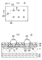
図1に示すMOSFET1の概略構成について説明する。MOSFET1は、主面10aに電界効果トランジスタが作り込まれて小形の平板形状に形成された半導体ペレット10と、前記電界効果トランジスタ要素を電気的に外部に引き出すための複数のインナリード35、36と、2つのインナリード35を支持するゲート用接続部片35a(インナリード連結部)と、ゲート用接続部片35aと半導体ペレット10とを電気的に接続する突起状端子(バンプ)から形成されたゲート用接続部(接続部)25と、6つのインナリード36を支持するソース用接続部片36a(インナリード連結部)と、ソース用接続部片36aと半導体ペレット10とを電気的に接続する突起状端子(バンプ)から形成されたソース用接続部(接続部)26と、インナリード35、36にそれぞれ接続された各アウタリード37、38と、放熱性能を高めるためのヘッダ28と、前記インナリード群およびヘッダ28の一部を樹脂封止した樹脂封止体29とからなる。
【0022】
したがって、図1のMOSFET1では、半導体ペレット10の主面10aには、インナリード35、36がそれぞれゲート用接続部片35a、ソース用接続部片36aを介してバンプから形成されたゲート用接続部25、ソース用接続部26によって機械的および電気的に接続されている。
【0023】
さらに、半導体ペレット10の主面10aと反対側の面(以降、この面を裏面10bと呼ぶ)には樹脂封止体29から露出するヘッダ28が機械的および電気的に接続され、一方、アウタリード37、38のそれぞれガル・ウイング形状に屈曲されている。
【0024】
なお、樹脂封止体29の内部において、半導体ペレット10の表面電極であるゲート用電極パッド19はゲート用のインナリード35にゲート用接続部25によって、半導体ペレット10の表面電極であるソース用電極パッド20はソース用のインナリード36にソース用接続部26によって、半導体ペレット10の裏面10b(下面)に形成されたドレイン用電極パッド21はヘッダ28にドレイン用接続部27によってそれぞれ機械的かつ電気的に接続されている。さらに、ヘッダ28の下面すなわち半導体ペレット10との接合面28aに対する反対側の面は、樹脂封止体29の下面において露出する露出面28bである。
【0025】
以上のMOSFETは、以下に述べるような製造方法によって製造されている。
【0026】
以下、MOSFETの製造方法を説明する。この説明によって前記MOSFETについての構成の詳細が明らかにされる。
【0027】
このMOSFETの製造方法においては、図2に示されている半導体ペレット10、図3に示されている多連リードフレーム30および図5に示されているヘッダ28が、半導体ペレット準備工程、リードフレーム準備工程およびヘッダ準備工程においてそれぞれ準備される。
【0028】
図2に示されている半導体ペレット10は、MOSFET1の製造工程の所謂前工程においてウエハ状態にてMOSFET要素を適宜作り込んだ後に、小さい正方形の薄板形状に分断(ダイシング)することにより製造したものである。この半導体ペレット10はサブストレート11を備えており、サブストレート11の上にはポリシリコンによってゲート12が下敷きシリコン酸化膜13を介して形成されている。サブストレート11におけるゲート12の外側に対応するサブストレート11の内部には半導体拡散層部としてのソース14が形成されており、サブストレート11の下部にはドレイン15が形成されている。
【0029】
サブストレート11の上にはCVD酸化膜等からなる絶縁膜16がゲート12およびソース14を被覆するように形成されており、この絶縁膜16におけるゲート12に対向する位置にはゲート用コンタクトホール17が一個、ゲート12に貫通するように開設されている。絶縁膜16におけるソース14に対向する領域にはソース用コンタクトホール18が複数個、ゲート用コンタクトホール17の片脇においてソース14にそれぞれ貫通するように開設されている。
【0030】
さらに、ゲート用コンタクトホール17の内部にはゲート用電極パッド19が形成され、各ソース用コンタクトホール18の内部にはソース用電極パッド20がそれぞれ形成されている。これら電極パッド19、20はアルミニウム系材料(アルミニウムまたはその合金)がスパッタリング蒸着等の手段により絶縁膜16の上に被着された後に、写真食刻法によってパターンニングされて形成されたものである。
すなわち、絶縁膜16の上に被着されたアルミニウム系材料は各コンタクトホール17、18の内部にそれぞれ充填されるため、この充填部によってそれぞれ形成された電極パッド19、20はゲート12およびソース14とにそれぞれ電気的に接続された状態になっている。他方、サブストレート11の下面にはドレイン用電極パッド21がアルミニウム系材料を被着されて形成されている。
【0031】
ゲート用電極パッド19および複数個のソース用電極パッド20の上には、リンシリケートガラスやポリイミド系樹脂等の絶縁材料からなる保護膜24が被着されており、保護膜24のゲート用電極パッド19およびソース用電極パッド20にそれぞれ対向する位置にはゲート用バンプ22および各ソース用バンプ23がそれぞれ突設されている。これらバンプ22、23は金(Au)線が使用されたスタッドバンプボンディング(SBB)法によって形成されたものである。すなわち、ネイルヘッド(熱圧着)式ワイヤボンディング装置またはネイルヘッド超音波(熱圧着)式ワイヤボンディング装置によって、パッドの上にワイヤ先端のボールが圧着(第一ボンディング)された後に、ボールとワイヤとの接続部位においてワイヤが引き千切られることによって形成されたバンプである。
【0032】
図3に示されている多連リードフレーム30は、鉄−ニッケル合金や燐青銅またはヘッダ28と同じ材質の銅合金等の導電性が良好な材料からなる薄板が用いられて、打抜きプレス加工またはエッチング加工等の手段により一体成形されている。この多連リードフレーム30には複数の単位リードフレーム31が一方向に一列に並設されている。但し、図3では、一つのMOSFET分(一単位分)のみを図示している。
【0033】
単位リードフレーム31は位置決め孔32aが開設されている外枠32を一対備えており、両外枠32、32は所定の間隔で平行になるように配されて一連にそれぞれ延設されている。隣合う単位リードフレーム31、31間には一対のセクション枠33、33が両外枠32、32の間に互いに平行に配されて一体的に架設されている。これら外枠、セクション枠によって形成される略長方形の枠体(フレーム)内に単位リードフレーム31が構成されている。
【0034】
単位リードフレーム31において、両セクション枠33、33の間には一対のダム部材34、34が互いに離間されてセクション枠33に直交するように一体的に架設されている。両ダム部材34、34の内側端辺における一端部にはゲート用インナリード35が一対、それぞれダム部材34と直角に一体的に突設されており、両ゲート用インナリード35、35間には矩形の平板形状のゲート用接続部片35aが一体的に形成されている。両ダム部材34、34の内側端辺における残りの部分にはソース用インナリード36が複数本(図示例では六本)、同数本(同じく三本)ずつ分配されて長さ方向に等ピッチをもってそれぞれ突設されており、対向するソース用インナリード36群間には長方形平板形状のソース用接続部片36aが一体的に形成されている。図示しないが、ゲート用接続部片35aとソース用接続部片36aの一主面の表面には錫(Sn)や金(Au)等を用いたメッキ処理が、半導体ペレット10に突設されたバンプ22、23による機械的かつ電気的接続作用が適正に実施されるように被着されている。
【0035】
両ダム部材34、34の外側端辺における両ゲート用インナリード35、35と対向する位置には、一対のゲート用アウタリード37、37が両ゲート用インナリード35、35の延長になるように突設されている。両ダム部材34、34の外側端辺における各ソース用インナリード36と対向する位置のそれぞれには、各ソース用アウタリード38が各ソース用インナリード36の延長になるようにそれぞれ突設されている。そして、隣合うアウタリード同士および両セクション枠33、33との間には、後述する樹脂封止体29の成形に際して図6に示すレジン(モールド用樹脂)60の流れを堰き止めるためのダム34aがそれぞれ形成されている。
【0036】
以上のように構成されたリードフレームには半導体ペレット10が、インナリードボンディング工程において図4に示されているようにボンディングされる。この際、多連リードフレーム30はボンディング装置(図示せず)によって一方向に歩進送りされる。そして、歩進送りされる多連リードフレーム30の途中に配設されているインナリードボンディングステージにおいて、半導体ペレット10は単位リードフレーム31に下方から対向されるとともに、各バンプ22および23が各インナリード35および36の接続部片35a、36aにそれぞれ整合されてボンディング工具により熱圧着されることにより、多連リードフレーム30に組み付けられる。
【0037】
すなわち、各バンプ22、23が各接続部片35a、36aに加熱下で押接されると、バンプ22、23が各接続部片35a、36aに熱圧着によって接続する。そして、半導体ペレット10のゲート用電極パッド19および各ソース用電極パッド20と、ゲート用インナリード35のゲート用接続部片35aおよびソース用インナリード36のソース用接続部片36aとの間には、ゲート用接続部25およびソース用接続部26がそれぞれ形成される。したがって、ゲート用接続部25によってゲート用電極パッド19とゲート用インナリード35とが機械的かつ電気的に接続され、一方、ソース用接続部26によってソース用電極パッド20とソース用インナリード36とが機械的かつ電気的に接続された状態になるとともに、これらの機械的接続によって半導体ペレット10が単位リードフレーム31に機械的に接続された状態すなわち固定的に組み付けられた状態になる。
【0038】
以上のようにして多連リードフレーム30にインナリードボンディングされた半導体ペレット10の反対側主面(以下、裏面10bという。)には、銅系材料(銅または銅合金)等の導電性および熱伝導性の良好な材料が用いられて図5に示されているように半導体ペレット10よりも若干大きめの長方形の平板形状に形成されたヘッダ28が機械的かつ電気的に接続される。すなわち、ヘッダ28の上面(半導体ペレット側の接合面28a)にAgペースト等の導電性および熱伝導性の良好な接着材が塗布された後に、半導体ペレット10の裏面10bが当接されて接着される。これにより、半導体ペレット10のドレイン用電極パッド21とヘッダ28とを機械的かつ電気的に接続するドレイン用接続部27が、この接着材層によって形成された状態になる。
【0039】
以上のようにして組み立てられたヘッダ付き半導体ペレット10と多連リードフレーム30との組立体には、樹脂封止体成形工程においてエポキシ樹脂等の絶縁性樹脂からなる樹脂封止体29が、図6に示されているトランスファ成形装置50を使用されて各単位リードフレーム31について同時成形される。
【0040】
図6に示されているトランスファ成形装置50は、シリンダ装置等(図示せず)によって互いに型締めされる一対の上型51と下型52とを備えており、上型51と下型52との合わせ面61には上型キャビティー凹部53aと、下型キャビティー凹部53bとが互いに協働してキャビティー53を形成するように複数組(一組のみが図示されている。)没設されている。
【0041】
上型51の合わせ面61にはポット54が開設されており、ポット54にはシリンダ装置(図示せず)により進退されるプランジャ55が成形材料としてのモールド樹脂すなわちレジン60を送給し得るように挿入されている。下型52の合わせ面61にはカル56がポット54との対向位置に配されて没設されている。カル56にはレジン60をキャビティー53に注入するためのゲート57の一端部が接続されており、ゲート57の他端部は下型キャビティー凹部53bに接続されている。下型キャビティー凹部53bのゲート57と対向する対辺にはスルーゲート58が接続されており、スルーゲート58は隣接した下型キャビティー凹部53bの対向辺に接続されている。スルーゲート58は上流側のキャビティー53に充填されたレジン60を流通(スルー)させて下流側のキャビティー53に充填して行くように構成されている。下型52の合わせ面61には逃げ凹所59が単位リードフレーム31の厚みを逃げ得るように、多連リードフレーム30の外形よりも若干大きめの長方形で、その厚さと略等しい寸法の一定深さに没設されている。
【0042】
以上のように構成されたトランスファ成形装置50による樹脂封止体29の成形作業に際して、前記構成にかかる組立体は下型52に没設された逃げ凹所59内に、半導体ペレット10が下型キャビティー凹部53b内にそれぞれ収容されるように配されてセットされる。
【0043】
続いて、上型51と下型52とが型締めされると、単位リードフレーム31における両セクション枠33、33および両ダム部材34、34が上型51と下型52との合わせ面61によって強く押さえられた状態になるため、図6に示されているように、ヘッダ28の下面(露出面28b)は下型キャビティー凹部53bの底面上に密着される。すなわち、両セクション枠33、33および両ダム部材34、34が押さえられることによって全周が保持された状態になるため、ヘッダ28の下面はインナリード35、36群の弾性力によって下型キャビティー凹部53bの底面に強く押接された状態になる。
【0044】
その後、ポット54からプランジャ55によってレジン60がゲート57およびスルーゲート58を通じて各キャビティー53に順次送給されて充填されて行く。この際、ヘッダ28の下面は下型キャビティー凹部53bの底面に密着された状態になっていることにより、レジン60がヘッダ28の下面に漏洩することが防止されるため、ヘッダ28の下面の外周縁に薄いレジンばり(レジンフラッシュ)が発生するのを防止することができる。
【0045】
充填後、レジン60が熱硬化されて樹脂封止体29が成形されると、上型51および下型52は型開きされるとともに、エジェクタ・ピン(図示せず)により樹脂封止体29が離型される。
【0046】
図7は樹脂封止体成形後の多連リードフレーム30と樹脂封止体29との組立体を示している。この組立体の樹脂封止体29の内部には、半導体ペレット10、インナリード35、36群と共に、半導体ペレット10の裏面10bに結合されたヘッダ28の一部(側面)も樹脂封止された状態になっている。この状態において、ヘッダ28はその半導体ペレット側の接合面28aと反対側の端面が樹脂封止体29の表面から露出した状態になっている。すなわち、ヘッダ28の半導体ペレット側の接合面28aと反対側には樹脂封止体29から露出した露出面28bが形成され、さらに、アウタリード37、38群は樹脂封止体29の長辺側の両側側面から直角に突出した状態になっている。
【0047】
以上のようにして樹脂封止体29を成形された組立体は、半田メッキ処理が施された後に、リードフレーム切断成形工程において、外枠32、セクション枠33、ダム34aを切り落とされるとともに、アウタリード37、38がガル・ウイング形状に屈曲される。これにより、図1に示されているMOSFET1が製造されたことになる。
【0048】
すなわち、図1に示されているMOSFET1のパッケージ2は、半導体ペレット10と複数本のインナリード35、36とヘッダ28の一部を樹脂封止した樹脂封止体29および複数本のアウタリード37、38を備えており、樹脂封止体29は長方形の平盤形状に形成されている。アウタリード37、38は樹脂封止体29の長辺側の二つの側面に等間隔に並べられてガル・ウイング形状に屈曲されている。樹脂封止体29の内部において、半導体ペレット10のゲート用電極パッド19はゲート用インナリード35にゲート用接続部25によって、半導体ペレット10のソース用電極パッド20はソース用インナリード36にソース用接続部26によって、半導体ペレット10の裏面10bに形成されたドレイン用電極パッド21はヘッダ28にドレイン用接続部27によってそれぞれ機械的かつ電気的に接続されている。ヘッダ28の下面は樹脂封止体29の下面において露出した状態で露出面28bとなっており、ヘッダ28のこの露出面28bの外周縁にはレジンばりは発生していない。
【0049】
以上のように製造され構成されたMOSFET1は、プリント配線基板3に図8に示されているように表面実装される。すなわち、MOSFET1のゲート用アウタリード37はプリント配線基板3の本体4に形成されたゲート用ランド5に、ソース用アウタリード38はソース用ランド6に、ドレイン用電極パッド21が接続されたヘッダ28はドレイン用ランド7にそれぞれ整合されてリフロー半田付けされる。このようにMOSFET1はプリント配線基板3に表面実装されるため、外部抵抗分は大幅に低減されることになる。また、ヘッダ28がプリント配線基板3のドレイン用ランド7に半田付けされるため、外部抵抗分が大幅に低減されるばかりでなく、半導体ペレット10の発熱が熱伝導によってプリント配線基板3に放出されることにより、放熱性能が大幅に向上される。
【0050】
前記MOSFETによれば、次の効果が得られる。
【0051】
1) 各インナリード35、36を半導体ペレット10に各接続部25、26によって機械的かつ電気的に接続することにより、ボンディングワイヤによる電気的接続を廃止することができるため、ボンディングワイヤによる電気的接続に比べて外部抵抗分を低減することができ、その結果、MOSFET1の性能を高めることができる。
【0052】
2) また、ボンディングワイヤによる接続を廃止することにより、MOSFET1のパッケージ2を小形軽量化することができるため、前記外部抵抗分を低減する効果とあいまって、MOSFET1の性能を高めることができる。
【0053】
3) ヘッダ28がインナリード群とは別体になっているため、インナリード35、36の材質に無関係に放熱性能の良好な材質を用いてヘッダ28を形成することにより、ヘッダ28の放熱性能を高めることができる。また、インナリード35、36はヘッダ28の材質に無関係にインナリード特性に最適の材質を選定することができるため、MOSFET1の品質および信頼性をより一層高めることができる。
【0054】
4) ソース用電極パッド20およびソース用インナリード36のソース用接続部26を複数個設けることにより、ソースに大電流を流すことができるため、MOSFET1の性能をより一層高めることができる。
【0055】
5) ガル・ウイング形状に形成したアウタリード37、38および半導体ペレット10を機械的かつ電気的に接続したヘッダ28をプリント配線基板3に表面実装することにより、外部抵抗分をさらに低減することができるとともに、ヘッダ28の放熱性能をさらに向上することができる。
【0056】
6) アウタリード37、38を樹脂封止体29の対向する二つの側面に分配して配置することにより、樹脂封止体29のトランスファ成形に際してアウタリード37、38を成形型(上型51と下型52)の合わせ面61によって両持ちして樹脂モールドすることができ、これにより、ヘッダ28を成形型の底面に密着させることができるため、樹脂封止体29から露出したヘッダ28の露出面28bの外周縁にレジンばりが発生するのを防止することができる。
【0057】
また、ヘッダ28が曲げ加工されることなく平板形状に形成され、かつ、ヘッダ28の露出面28bとアウタリード37、38の被実装面37a、38aとがほぼ同一高さの面であることにより、MOSFET1の実装高さを低くすることができる。これにより、高い出力で、かつ、高発熱のMOSFET1においてその実装高さに制限がある場合などにおいても、実装高さを抑えることが可能になる。
【0058】
次に、本発明の実施の形態を、図9〜図12のMOSFETの構造を示す図、図13〜図22のMOSFETの製造方法を示す図、図23〜図25のMOSFETによる作用効果を説明する図、図27の比較例のMOSFETのヘッダフレームとヘッダフレーム搭載図を用いて説明する。
【0059】
なお、図11(a)、図12、図23および図24(a)のそれぞれの平面図では、同一の部材を同一のハッチングによって示している。
【0060】
本実施の形態の半導体装置であるMOSFET70は、前記のMOSFET1と同様に、高出力かつ高発熱のパワーMOSトランジスタである。
【0061】
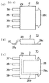
なお、MOSFET70は、樹脂封止体29の対向する二つの側面のうち、図9(b)に示すように、一方の側面からはガル・ウイング形状に屈曲された三つのソース用のアウタリード38と一つのゲート用のアウタリード37が突出し、かつ、この側面に対向する他方の側面からは、図9(a)に示すように平板形状の略四角形のヘッダ突出部28cが突出している。
【0062】
すなわち、本実施の形態のMOSFET70の図1のMOSFET1との外観構造の差は、図1のMOSFET1では樹脂封止体29の対向する両側面にガル・ウイング形状のアウタリード37、38を配置したのに対し、本実施の形態のMOSFET70では樹脂封止体29の片方の側面にはガル・ウイング形状のアウタリード37、38は配置せず、その代わりとして、図10(a)、(b)に示すように、前記片方の側面に平板形状のヘッダ突出部28cを配置したことである。
【0063】
なお、MOSFET70においても、ヘッダ28の下面すなわちヘッダ28の半導体ペレット10に接合する面と反対側の面には、図10(c)に示すような樹脂封止体29から露出する露出面28bが形成されている。
【0064】
続いて、本実施の形態のMOSFET70の詳細構造について説明する。
【0065】
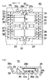
図9〜図12に示すように、MOSFET70は主面10aに電界効果トランジスタが形成された半導体ペレット10の図2に示すゲート用電極パッド19(表面電極)に電気的に接続されたゲート用のインナリード35および図2に示すソース用電極パッド20(表面電極)に電気的に接続されたソース用のインナリード36と、半導体ペレット10のゲート用電極パッド19とインナリード35を支持するゲート用接続部片35aとを電気的に接続するバンプからなる突起状端子であるゲート用接続部25と、半導体ペレット10のソース用電極パッド20とインナリード36を支持するソース用接続部片36aとを電気的に接続するバンプからなる突起状端子であるソース用接続部26と、半導体ペレット10およびインナリード35、36を樹脂封止して形成された樹脂封止体29と、インナリード35に接続され、かつ樹脂封止体29の一方の側面から突出したアウタリード37と、インナリード36に接続され、かつ樹脂封止体29の前記側面と同一側面からアウタリード37と並んで突出したアウタリード38と、半導体ペレット10の主面10aと反対側の面(裏面10b)にヘッダ接合材である銀ペースト39(図1のMOSFET1では、ドレイン用接続部27のこと)を介して接合し、かつ、樹脂封止体29のアウタリード37、38の突出側の側面と反対側の側面(他方の側面)に突出するヘッダ突出部28cを備えたヘッダ28とからなる。
【0066】
つまり、本実施の形態のMOSFET70は、平板形状のヘッダ28にヘッダ突出部28cが設けられているため、ヘッダ28の面積を大幅に増加させることができ、これにより、半導体ペレット10から発生する熱をヘッダ突出部28cを有したヘッダ28から大幅に逃がすことが可能になる。その結果、MOSFET70の低熱抵抗化をさらに図ることができる。
【0067】
なお、ヘッダ28の面積を大幅に増加させることができるため、電気的抵抗値を下げることができ、これにより、前記低熱抵抗化の効果と合わせてMOSFET70の電気的特性を向上できる。
【0068】
また、インナリード35、36のうち、ソース用のインナリード36は、半導体ペレット10の主面10aと対向して配置されたソース用の接続部片36a(インナリード連結部)から三本に分割されて設けられている。つまり、図11(a)に示すように、それぞれのインナリード35、36は、それぞれゲート用接続部片35a(インナリード連結部)、ソース用接続部片36a(インナリード連結部)に連結され、かつ支持されている。
【0069】
これにより、モールド後、インナリード36に繋がったアウタリード38を切断・成形する際に、インナリード36が分割されているため、これらインナリード36を支持しているソース用接続部片36aに掛かる応力を分散させて緩和させることができる。その結果、インナリード連結部であるソース用接続部片36aから突起状端子であるソース用接続部26が剥がれて接続不良を引き起こすことを防げる。さらに、インナリード36が分割されて支持されていることにより、インナリード36と樹脂封止体29との接触面積が増え、これにより、パッケージ2の内部への吸湿もしにくくなり、その結果、MOSFET70の耐湿性を向上できる。
【0070】
なお、ソース用のインナリード36が半導体ペレット10の主面10aと対向して配置されたソース用のソース用接続部片36a(インナリード連結部)から三つに分割されて設けられている場合であっても、前記分割による電気的抵抗増加値は僅かであり、この電気的抵抗増加値は前記電界効果トランジスタのオン抵抗値より小さいため、本実施の形態のMOSFET70のようにアウタリード38を複数(三本)に分割して配置できる。
【0071】
また、MOSFET70はヘッダ28の半導体ペレット10との接合面28aと反対側の面が樹脂封止体29から露出する露出面28bであり、かつ、アウタリード37、38が屈曲されるとともに、ヘッダ28の露出面28bとアウタリード37、38の被実装面37a、38aとがほぼ同一の高さ(アウタリード厚さ以下)に設けられた面実装形のものである。したがって、MOSFET70をプリント配線基板3(図8参照)等に実装する際には、アウタリード差し込み形の半導体装置とは異なり、MOSFET70を吸着保持等によって移し換えるだけであり、実装を容易にできる。
【0072】
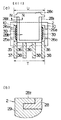
また、本実施の形態のMOSFET70では複数のアウタリード37、38のうち、図24(a)に示すように、両端部に配置された二つのアウタリード37、38の外側側部間の距離(T)と、ヘッダ28におけるヘッダ突出部28cのアウタリード配列方向の幅(U)とがほぼ同じ長さで形成されている。これは、前記プリント配線基板3に形成されている従来のフットパターン(基板端子)との共有化を図るものであり、これにより、MOSFET70をプリント配線基板3上に実装する際に、従来のフットパターンを変えることなく、そのまま実装することができる。
【0073】
また、図24(a)、(b)に示すように、ヘッダ28およびヘッダ突出部28cの外周の一部(側面を含む少なくとも樹脂封止体29と接合する箇所)には、段差部28fが設けられている。これにより、樹脂封止体29とヘッダ28との接合面積を増加させることができ、その結果、両者の密着性を向上できる。したがって、樹脂封止体29へのクラックの形成を防止でき、これにより、MOSFET70の品質を向上することができる。
【0074】
また、本実施の形態のMOSFET70では、三本のソース用のインナリード36を支持するソース用接続部片36a(インナリード連結部)が半導体ペレット10の主面10aの上にこれに対向して配置され、かつ、それぞれのインナリード35、36の基端部35b、36bが半導体ペレット10の主面10aにおける内側領域上に配置されている。これは、MOSFET70の製造工程においてモールドを行う前の段階で、ヘッダ接合材である銀ペースト39の外観検査を行う際に、図23(a)に示すように、隣合ったインナリード間の隙間から銀ペースト39の有無を検査することを可能にするものである。
【0075】
さらに、それぞれのインナリード35、36の基端部35b、36bを半導体ペレット10の主面10aにおける内側領域上に配置することにより、図25に示すようにアウタリード37、38の長さ(W)を長く形成することができる。これにより、アウタリード37、38の曲げ成形時のストレスを緩和することができるとともに、MOSFET70の耐湿テストなどにおける水分の半導体ペレット10までの侵入到達時間を長くすることができ、その結果、MOSFET70の吸湿性を向上できる。
【0076】
本実施の形態の半導体装置(MOSFET70)のその他の構造と、MOSFET70によって得られるその他の作用効果については、前記MOSFET1で説明したものと同様であるため、その重複説明は省略する。
【0077】
次に、本実施の形態のMOSFET70の製造方法を、図13に示す製造プロセスフロー図にしたがって説明する。
【0078】
まず、それぞれの半導体ペレット領域に電界効果トランジスタが形成された半導体ウエハ(図示せず)を準備する。
【0079】
続いて、図13のステップS1により、スタッドバンプ等のバンプ形成方法を用いて、ウエハ状態で各半導体ペレット10の図2に示すゲート用電極パッド19、ソース用電極パッド20にそれぞれゲート用バンプ22、ソース用バンプ23を形成する。なお、ゲート用バンプ22およびソース用バンプ23は、例えば、Auや半田等によって形成されるものである。
【0080】
その後、ステップS2に示すダイシングを行って前記半導体ウエハを切断・分離し、これにより、図14に示すようなバンプ付け済みの個々の半導体ペレット10を取得する。
【0081】
続いて、主面10aに電界効果トランジスタが形成された半導体ペレット10を準備する。
【0082】
また、複数のインナリード35、36とこれらインナリード35、36にそれぞれ電気的に接続された複数のアウタリード37、38とが連結されてなるリードフレームを準備する。
【0083】
なお、本実施の形態で用いる前記リードフレームは、単一の半導体装置用領域である単位リードフレーム31が複数連なって設けられた多連リードフレーム30であり、さらに、本実施の形態においては、前記多連リードフレーム30として、前記単一の半導体装置用領域が、図16に示すような2行×2列のマトリクス配置による群を一つの纏まりとするマトリクスフレーム40の場合を説明する。つまり、図16に示すマトリクスフレーム40は、4個分のMOSFET70を一つの群とするものである。ただし、マトリクスフレーム40における前記一つの群内のマトリクスの数は、2行×2列に限定されるものではなく、これ以外の数であってもよい。
【0084】
なお、図16に示すマトリクスフレーム40では、四個分のMOSFET70を一つの群としたため、区画窓40aの両側で半導体ペレット10の向きを変える必要があり、半導体ペレット10の向きをQ点で点対称となるような配置にしている。
【0085】
また、平板形状に形成されたヘッダ28を準備する。
【0086】
本実施の形態のMOSFET70の製造方法では、四個のMOSFET70を一つの群として製造するため、四個分のMOSFET70に対応する四つのヘッダ28が2行×2列配置で一体に設けられた図15に示すようなヘッダフレーム41を用い、これにより、各ヘッダ28を半導体ペレット10に接合する際には、一体となった四つのヘッダ28を四つの半導体ペレット10のそれぞれに一緒に接合する(図15では、E部に示すヘッダ28が一つのMOSFET70に使用されるヘッダ28である)。
【0087】
さらに、一つのヘッダフレーム41には、ヘッダ付け時のヘッダ付け装置(図示せず)のガイドとの位置決め用の丸孔28dが四つ設けられ、そのうち、2つの丸孔28dがスリット28eと連通している。
【0088】
なお、MOSFET70の製造手順によれば、マトリクスフレーム40上に半導体ペレット10が存在しないとヘッダ28を配置することはできず、さらに、ヘッダ28を配置できないと、モールド工程におけるモールド装置の上型51および下型52の構造上レジン漏れが発生し、モールドのショット毎に上型51および下型52のクリーニングが必要になる。
【0089】
したがって、単品構造のヘッダ28や二つのヘッダ28を一体とした構造等のものを用いてMOSFET70を製造するのは好ましくなく、本実施の形態のように四つのヘッダ28を一体としたヘッダフレーム41を用いてMOSFET70を製造する方が好ましい。さらに、四つのヘッダ28を一体としたヘッダフレーム41を用いることにより、単品構造のヘッダ28や二つのヘッダ28を一体とした構造のものを用いる場合と比べてスループットを向上できる。
【0090】
また、ヘッダフレーム41を、図27(a)の比較例のヘッダフレーム42のように一列に三つのヘッダ28を連結させた構造のフレームも考えられるが、この場合、半導体ペレットのサイズが小さくなると、ヘッダ28の重さにより、図27(b)に示すように、ヘッダ28が傾く可能性があるため、このような三つのヘッダ28を一列に配置したヘッダフレーム42も好ましくない。
【0091】
その後、ステップS3に示すフリップチップにより、半導体ペレット10とマトリクスフレーム40とを接合するペレットボンディングを行う。
【0092】
ここでは、図17(a)、(b)に示すように、四つの半導体ペレット10の裏面10bをそれぞれ上方に向け、四つの半導体ペレット10をマトリクスフレーム40のそれぞれの半導体装置領域のゲート用接続部片35aおよびソース用接続部片36a上に配置し、熱圧着によってペレットボンディングを行う。
【0093】
すなわち、インナリード35を支持するゲート用接続部片35aと半導体ペレット10のゲート用電極パッド19(図2参照)とを、ゲート用電極パッド19に取り付けられたゲート用バンプ22(突起状端子)を熱圧着してゲート用接続部25によって接合し、これにより、ゲート用バンプ22およびゲート用接続部片35aを介してゲート用電極パッド19とインナリード35とを電気的に接続する。
【0094】
同様に、インナリード36を支持するソース用接続部片36aは半導体ペレット10のソース用電極パッド20(図2参照)とを、ソース用電極パッド20に取り付けられたソース用バンプ23(突起状端子)を熱圧着してソース用接続部26によって接合し、これにより、ソース用バンプ23およびソース用接続部片36aを介してソース用電極パッド20とインナリード36とを電気的に接続する。
【0095】
なお、図17に示す状態は、熱圧着直前の構造を示すものであり、これを熱圧着すると図17に示すソース用バンプ23が図18(b)に示すソース用接続部26となる。
【0096】
その際、ゲート用バンプ22およびソース用バンプ23は、それぞれインナリード35、36に取り付けられていてもよい。また、フリップチップ実装後の半導体ペレット10の主面10aとゲート用接続部片35aおよびソース用接続部片36aとの位置関係は、図17(c)に示すものと同様になる。
【0097】
つまり、本実施の形態のMOSFET70では、3本のソース用のインナリード36を支持するソース用接続部片36a(インナリード連結部)が半導体ペレット10の主面10aの上にこれに対向して配置され、かつ、各インナリード36の基端部36bが半導体ペレット10の主面10aにおける内側領域上に配置されている。さらに、1本のゲート用のインナリード35を支持するゲート用接続部片35aも半導体ペレット10の主面10a上にソース用接続部片36aと絶縁されてかつ並んで配置され、インナリード35の基端部35bも半導体ペレット10の主面10aにおける内側領域上に配置されている。
【0098】
続いて、ヘッダ28の半導体ペレット10への取り付けであるヘッダ付けを行う(ステップS4)。
【0099】
ここで、図18(a)、(b)に示すように、まず、各半導体ペレット10の裏面10bに、ヘッダ接合材である銀ペースト39を塗布する。続いて、図19(a)、(b)に示すように、4つの半導体ペレット10の各裏面10bにヘッダフレーム41の各ヘッダ28を載置する。さらに、半導体ペレット10を加圧するとともに、スクラブなどを行って、これにより、各ヘッダ28と各半導体ペレット10の裏面10bとをそれぞれ銀ペースト39を介して接合する。
【0100】
その後、この段階で、図23(a)に示すように、隣あったインナリード間の隙間から、およびソース用接続部片36aのインナリード配置側と反対の辺側からヘッダ接合材である銀ペースト39の有無を外観検査し、これにより、銀ペースト39の濡れ性を検査する。これは、図23(a)に示すソース用接続部片36aの幅寸法Sが、半導体ペレット10の前記幅Sと対応する幅より小さく形成されているため、銀ペースト39が半導体ペレット10よりはみ出ているかどうかを確認するものであり、はみ出ている場合に合格とするものである。
【0101】
さらに、マトリクスフレーム40の表裏を反転させることにより、図23(b)に示すように、ヘッダ28のアウタリード配列方向と同方向の両側部から銀ペースト39を外観検査する。これにより、ヘッダ28の前記両側部から銀ペースト39を外観検査し、銀ペースト39が見える場合には、銀ペースト39の濡れ性を合格とする。これは、図23(b)に示すように、ヘッダ28において前記アウタリード配列方向と同方向の幅(V)が半導体ペレット10の同方向の長さより狭く形成されていることにより、銀ペースト39がヘッダ28よりはみ出ているかどうかを確認するものである。
【0102】
なお、ソース用接続部片36aとゲート用接続部片35aとを半導体ペレット10より小さくすることにより、MOSFET70のプリント配線基板3(図8参照)へのリフロー実装時などに半導体ペレット10にかかる応力を緩和できる。
【0103】
その後、図13に示すステップS5のモールドを行う。ここでは、図20(a)、(b)、(c)に示すように、半導体ペレット10、インナリード群およびヘッダ28を上型51および下型52のキャビティー53に配置し、この状態で型締めを行った後、キャビティー53にレジン60を注入して樹脂封止(モールド)する。
【0104】
この際、ヘッダフレーム41がキャビティー53に対応して2×2配列であるため、フリップチップ実装後に脱落した半導体ペレット10があっても、キャビティー53からのレジン漏れの発生を防止できる。また、図21に示すように、ヘッダ28の露出面28bが上型51のキャビティー底面に密着した状態でレジン注入が行われるため、レジン硬化後に、ヘッダ28の半導体ペレット10との接合面28aと反対側の面すなわち露出面28bを樹脂封止体29から露出させることができ、さらに、アウタリード37、38の突出方向と反対の方向にヘッダ突出部28cを突出させて樹脂封止体29を形成できる。
【0105】
その後、図22(a)に示すように、複数のアウタリード37、38をマトリクスフレーム40から切断して屈曲する切断・成形を行う(ステップS6)。
【0106】
これと同時に、一体化されていたヘッダフレーム41を4つのそれぞれの丸孔28dで切断し、スリット28eを介して4つのヘッダ28に分離する。また、この切断・成形工程では、アウタリード37、38を図22(b)に示すように、ガル・ウイング形状に屈曲する。
【0107】
なお、半導体ペレット10の主面10a上にソース用接続部片36aおよびゲート用接続部片35aが配置され、これらに支持されたインナリード35、36のそれぞれの基端部35b、36bも主面10a上に配置されていることにより、アウタリード曲げ成形の際にバンプ接合部であるゲート用接続部25およひソース用接続部26に掛かる応力を低減できる。
【0108】
さらに、図25に示すP部のように、ゲート用接続部片35aおよびソース用接続部片36aにそれぞれ細いリード25a、26aが設けられていることにより、アウタリード切断時に細リード25a、26aが伸びるため、前記バンプ接合部であるゲート用接続部25およびソース用接続部26に掛かる応力を緩和できる。
【0109】
その結果、アウタリード切断・成形時に前記バンプ接合部にかかる曲げ応力を緩和できる。
【0110】
これにより、MOSFET70の製造を終了する。なお、MOSFET70の製造工程において、ステップS3のフリップチップからステップS6の切断・成形までは、ヘッダ28の露出面28b側を上方に向けて工程間移動させる。
【0111】
ここで、本実施の形態の半導体装置(MOSFET70)のその他の製造方法については、前記参考例のMOSFET1の製造方法と同様であり、その重複説明は省略する。
【0112】
さらに、本実施の形態のMOSFET70の製造方法によって得られるその他の作用効果については、前記参考例で説明したものと同様であるため、その重複説明は省略する。
【0113】
以上、本発明者によってなされた発明を実施の形態に基づき具体的に説明したが、本発明は前記実施の形態に限定されるものではなく、その要旨を逸脱しない範囲で種々変更可能であることはいうまでもない。
【0114】
例えば、前記実施の形態では、ソース用のアウタリード38が複数に分離されてそれぞれがゲート用のアウタリード37とほぼ同様の幅で形成されている場合を説明したが、図26の変形例のMOSFET80のように、樹脂封止体29の両側に配置されるソース用のアウタリード38が一体となってゲート用のアウタリード37より幅広に形成されていてもよい。これにより、電気的抵抗値を低減(例えば、約0.1mΩ程度)することができ、その結果、MOSFET80の電気的特性を向上できるとともに、放熱性も向上できる。
【0115】
また、バンプ(ゲート用バンプ22やソース用バンプ23)は半導体ペレット側に配設するに限らず、インナリード側に配設してもよい。その際、前記バンプはSSB法によって形成するに限らず、メッキ法等によって形成してもよい。さらに、前記バンプは金によって形成するに限らず、半田等によって形成してもよい。
【0116】
半導体ペレット10とヘッダ28とは、銀ペースト等の導電性接着材によって接続するに限らず、半田付けによって接続してもよいし、金−錫共晶層等によって接続してもよい。但し、半導体ペレット10のヘッダ28への導電性および放熱性を配慮して、導電性および熱伝導性の良好な材料を選定することが望ましい。
【0117】
ヘッダ28にはドレイン用電極パッド21を接続するに限らず、ソース用電極パッド20を接続してもよい。
【0118】
ヘッダ28は半導体ペレット10にインナリードボンディング後に接続するに限らず、インナリードボンディング前またはインナリードボンディングと同時に半導体ペレット10に接続してもよい。
【0119】
ヘッダ28の形状、大きさ、構造等は、要求される放熱性能、半導体ペレット10の性能、大きさ、形状、構造等々の諸条件に対応して選定することが望ましい。
【0120】
また、ヘッダ28を形成する材料としては銅系材料を使用するに限らず、アルミニウム系等の熱伝導性の良好な他の金属材料を使用することができる。
また、本発明は、IGBT(Insulating Gate Bipolar Transistor)や、高出力のバイポーラトランジスタのような3端子のトランジスタ用パッケージにも適用できる。
【図面の簡単な説明】
【図1】 本発明の参考例であるMOSFETを示しており、(a)は一部切断平面図、(b)は一部切断正面図、(c)は一部切断側面図である。
【図2】 そのMOSFETの製造方法に使用される半導体ペレットを示しており、(a)は平面図、(b)は(a)のb−b線に沿う拡大断面図である。
【図3】同じく多連リードフレームを示しており、(a)は一部省略平面図、(b)は正面断面図である。
【図4】インナリードボンディング後を示しており、(a)は一部省略平面図、(b)は正面断面図である。
【図5】ペレットボンディング後を示しており、(a)は一部省略平面図、(b)は正面断面図である。
【図6】樹脂封止体成形工程を示しており、(a)は一部省略正面断面図、(b)は(a)のb−b線に沿う断面図である。
【図7】樹脂封止体成形後を示しており、(a)は一部省略平面図、(b)は正面断面図である。
【図8】 図1に示すMOSFETの実装後を示しており、(a)は平面図、(b)は一部切断正面図である。
【図9】 本発明の実施の形態の半導体装置であるMOSFETの構造の一例を示す図であり、(a)はヘッダ突出部側から眺めた外観斜視図、(b)はアウタリード側から眺めた外観斜視図である。
【図10】図9に示すMOSFETの構造を示す図であり、(a)は平面図、(b)は正面図、(c)は底面図である。
【図11】図9に示すMOSFETの構造を示す図であり、(a)は樹脂封止体(パッケージ)を透過してその内部構造を示す平面図、(b)は(a)のC−C線に沿う断面図、(c)は(a)のD−D線に沿う断面図である。
【図12】図9に示すMOSFETの樹脂封止体(パッケージ)を透過してその内部構造を示す底面図である。
【図13】図9に示すMOSFET製造工程の一例を示すプロセスフロー図である。
【図14】図9に示すMOSFETに用いられる半導体ペレットの構造の一例を示す平面図である。
【図15】図9に示すMOSFETの組み立てに用いられるヘッダフレームの構造の一例を示す平面図である。
【図16】図9に示すMOSFETの組み立てに用いられるマトリクスフレームの構造の一例を示す部分平面図である。
【図17】図9に示すMOSFETの製造工程におけるフリップチップ実装時の構造の一例を示す図であり、(a)は部分平面図、(b)は(a)のF−F線に沿う断面図、(c)は(a)のG部をリード側から眺めた部分底面図である。
【図18】図9に示すMOSFETの製造工程における銀ペースト付け時の構造の一例を示す図であり、(a)は部分平面図、(b)は(a)のH−H線に沿う断面図である。
【図19】図9に示すMOSFETの製造工程におけるヘッダ付け時の構造の一例を示す図であり、(a)は部分平面図、(b)は(a)のI−I線に沿う断面図である。
【図20】図9に示すMOSFETの製造工程におけるモールド時の構造の一例を示す図であり、(a)は成形金型内の状態を成形金型を透過して示す部分平面図、(b)は成形金型を型締めした際の(a)のJ−J線に沿う部分断面図、(c)は成形金型を型締めした際の(a)のK−K線に沿う部分断面図である。
【図21】成形金型を型締めした際の図20(a)のL−L線に沿う拡大部分断面図である。
【図22】図9に示すMOSFETの製造工程における切断・成形時の構造の一例を示す図であり、(a)は部分平面図、(b)は(a)のM−M線に沿う断面図である。
【図23】(a)、(b)は図9に示すMOSFETの製造工程における銀ペースト塗布の検査方法の一例を示す部分平面図である。
【図24】図9に示すMOSFETにおけるヘッダの段差部の構造の一例を示す図であり、(a)は樹脂封止体を透過して示す平面図、(b)は(a)のN−N線に沿う部分拡大断面図である。
【図25】図9に示すMOSFETに用いられるインナリードの細リードの構造の一例を示す平面図である。
【図26】本発明の図9MOSFETの変形例の構造を示す一部切断平面図である。
【図27】本発明の半導体装置であるMOSFETに対する比較例のMOSFETに用いられるヘッダフレームとそのヘッダ付け状態を示す図であり、(a)はヘッダフレームの平面図、(b)は(a)のヘッダフレームを用いてヘッダ付けを行った際の部分断面図である。
【符号の説明】
1…MOSFET、2…パッケージ、3…プリント配線基板、4…本体、5…ゲート用ランド、6…ソース用ランド、7…ドレイン用ランド、10…半導体ペレット、10a…主面、10b…裏面、11…サブストレート、12…ゲート、13…シリコン酸化膜、14…ソース、15…ドレイン、16…絶縁膜、17…ゲート用コンタクトホール、18…ソース用コンタクトホール、19…ゲート用電極パッド、20…ソース用電極パッド、21…ドレイン用電極パッド、22…ゲート用バンプ、23…ソース用バンプ、24…保護膜、25…ゲート用接続部、26…ソース用接続部、25a、26a…細リード、27…ドレイン用接続部、28…ヘッダ、28a…接合面、28b…露出面、28c…ヘッダ突出部、28d…丸孔、28e…スリット、28f…段差部、29…樹脂封止体、30…多連リードフレーム、31…単位リードフレーム、32…外枠、32a…位置決め孔、33…セクション枠、34…ダム部材、34a…ダム、35、36…インナリード、35a…ゲート用接続部片、36a…ソース用接続部片、35b、36b…基端部、37、38…アウタリード、37a、38a…被実装面、39…銀ペースト、40…マトリクスフレーム、40a…区画窓、41…ヘッダフレーム、42…ヘッダフレーム、50…トランスファ成形装置、51…上型、52…下型、53…キャビティー、53a…上型キャビティー、53b…下型キャビティー、54…ポット、55…プランジャ、56…カル、57…ゲート、58…スルーゲート、59…凹所、60…レジン、61…合わせ面、70…MOSFET、80…MOSFET。[0001]
BACKGROUND OF THE INVENTION
The present invention relates to a semiconductor manufacturing technique, and more particularly to a technique effective when applied to a high-power MOSFET (metal oxide semiconductor field effect transistor).
[0002]
[Prior art]
According to a study by the inventors, as an example of a semiconductor device with high output and high heat generation, there is a transistor called MOSFET, which is a power source or switch of a battery drive device, an automobile electrical component, a motor drive control device. It is used in all fields of electronic equipment and electrical equipment. Japanese Patent Laid-Open No. 8-64634 discloses an example of such a high output and high heat generation MOSFET. In this MOSFET, a field effect transistor (MOSFET element) is formed and a semiconductor pellet formed in a small flat plate shape is electrically connected to a surface electrode of the semiconductor pellet, and the MOSFET element is electrically connected It has a plurality of inner leads for pulling out to the outside, a header for improving heat dissipation performance, a resin pellet, an inner lead group, and a resin sealing body formed by resin sealing a part of the header, Each inner lead is mechanically and electrically connected to the main surface, which is the circuit forming surface of the semiconductor pellet, via a protruding terminal, and on the back surface, which is the surface opposite to the main surface of the semiconductor pellet. The header is joined.
[0003]
In this MOSFET, since each inner lead is electrically connected to the surface electrode of the semiconductor pellet via the protruding terminal, the external resistance can be reduced as compared with the electrical connection by the bonding wire. In addition, since the header is separate from the inner lead group, the header can be formed using a material with good heat dissipation performance regardless of the material of the inner lead, thereby improving the heat dissipation performance of the header. Can do.
[0004]
[Problems to be solved by the invention]
By the way, in the MOSFET, the electrical resistance of the bonding wire and the electrical resistance of the aluminum wiring of the semiconductor pellet (hereinafter referred to as external resistance), and the resistance inside the semiconductor pellet (hereinafter referred to as internal resistance). Is the on-resistance of the entire MOSFET. Here, the external resistance component hardly poses a problem at the stage where the internal resistance component is large. However, when technological innovation progresses and the internal resistance component is improved so that the external resistance component becomes smaller and the external resistance component exceeds about 50% of the total, the external resistance component cannot be ignored.
[0005]
In the MOSFET, each inner lead is electrically connected to the surface electrode of the semiconductor pellet through a protruding terminal, so that the external resistance can be reduced as compared with the electrical connection using a bonding wire. Since the outer lead connected to each of the leads becomes long, there is a problem that the effect of reducing the external resistance is reduced accordingly.
[0006]
An object of the present invention is to provide a semiconductor device and a method for manufacturing the same that can greatly reduce the external resistance.
[0007]
Another object of the present invention is to provide a semiconductor device and a method for manufacturing the same that can reduce thermal resistance and mounting height.
[0008]
The above and other objects and novel features of the present invention will be apparent from the description of this specification and the accompanying drawings.
[0009]
[Means for Solving the Problems]
The semiconductor device of the present invention is a semiconductor pellet formed in a small flat plate shape with a field effect transistor element formed on the main surface,
A plurality of inner leads for electrically pulling out the field effect transistor element to the outside;
Each outer lead connected to the inner lead,
A header to improve heat dissipation performance,
A resin sealing body in which a part of the inner lead group and the header is resin-sealed,
Each of the inner leads is mechanically and electrically connected to the main surface of the semiconductor pellet by a connecting portion formed from a projecting terminal, and the resin on the surface opposite to the main surface of the semiconductor pellet. The header exposed from the sealing body is mechanically and electrically connected, and each of the outer leads is bent into a gull wing shape.
[0010]
Thereby, since the inner lead connection part which supports each inner lead is directly connected to the semiconductor pellet by each connection part, an external resistance component can be reduced compared with the electrical connection by a bonding wire. Further, since the outer lead formed in a gull wing shape and the header mechanically and electrically connected to the semiconductor pellet can be surface-mounted on the printed circuit board, the external resistance can be further reduced. .
[0011]
In addition, since the header is separate from the inner lead group, the heat dissipation performance of the header can be enhanced by forming the header using a material having good heat dissipation performance regardless of the material of the inner lead. Furthermore, by surface mounting the header on the printed wiring board, the heat from the semiconductor pellet can be effectively released to the printed wiring board by heat conduction, and as a result, the heat dissipation performance can be further enhanced.
[0012]
The semiconductor device of the present invention includes a plurality of inner leads electrically connected to a surface electrode of a semiconductor pellet having a field effect transistor formed on a main surface, and the surface electrode and the inner lead of the semiconductor pellet. A connecting portion for electrical connection, a resin sealing body formed by resin-sealing the semiconductor pellet and the inner lead, and connected to the inner lead and protruding side by side from the same side surface of the resin sealing body A header including a plurality of outer leads and a header protruding portion that is bonded to a surface opposite to the main surface of the semiconductor pellet and protrudes to a side surface opposite to the protruding side surface of the outer lead of the resin sealing body. The surface of the header opposite to the bonding surface with the semiconductor pellet is exposed from the resin sealing body, and the outer lead is bent.
[0013]
Thereby, since the header protrusion is provided in the header, the area of the header can be greatly increased, and thus heat generated from the semiconductor pellet can be greatly released from the header having the header protrusion. . As a result, it is possible to further reduce the thermal resistance of the semiconductor device.
[0014]
The semiconductor device of the present invention includes a plurality of inner leads electrically connected to a surface electrode of a semiconductor pellet having a field effect transistor formed on a main surface, and the surface electrode and the inner lead of the semiconductor pellet. A connecting portion for electrical connection, a resin sealing body formed by resin-sealing the semiconductor pellet and the inner lead, and connected to the inner lead and protruding side by side from the same side surface of the resin sealing body A header including a plurality of outer leads and a header protruding portion that is bonded to a surface opposite to the main surface of the semiconductor pellet and protrudes to a side surface opposite to the protruding side surface of the outer lead of the resin sealing body. A surface of the header opposite to the joint surface with the semiconductor pellet is an exposed surface exposed from the resin sealing body, the outer lead is bent, and the And the exposed surface and the mounting surface of the outer lead Da are those provided at substantially the same height.
[0015]
The method for manufacturing a semiconductor device of the present invention includes a step of preparing a semiconductor pellet formed in a small flat plate shape with a field effect transistor formed on a main surface, a plurality of inner leads, and a connection to each of the inner leads. A step of preparing a lead frame connected to each of the outer leads, a step of preparing a header formed in a flat plate shape using a material having good conductivity and heat conductivity, and Mechanically and electrically connecting to the semiconductor pellet by a connecting portion formed by a projecting terminal on the inner lead side or the semiconductor pellet side, and mechanically connecting the surface opposite to the main surface of the semiconductor pellet to the header And electrically connecting the semiconductor pellet, the inner lead group and a part of the header with resin sealing A step of forming a Aburafutometai, and a step of bending a plurality of the outer leads to the gull-wing shape.
[0016]
Furthermore, the semiconductor device manufacturing method of the present invention includes a step of preparing a semiconductor pellet having a field effect transistor formed on a main surface, a plurality of inner leads, and a plurality of outer leads electrically connected to the inner leads, respectively. A step of preparing a lead frame connected to each other, a step of preparing a header formed in a flat plate shape, and the inner lead and the surface electrode of the semiconductor pellet by a projecting terminal on the inner lead side or the semiconductor pellet side Electrically connecting through the formed connecting portion, joining the header and the surface opposite to the main surface of the semiconductor pellet, the semiconductor pellet, the inner lead group, and the header A portion of the header is sealed with resin to expose the surface of the header opposite to the bonding surface with the semiconductor pellet. Those with a step by projecting a header projecting portion in a direction opposite to the projecting direction of the lead to form a resin sealing body, and a step of bending a plurality of outer leads.
[0017]
DETAILED DESCRIPTION OF THE INVENTION
In the following embodiments, the description of the same or similar parts will not be repeated in principle unless particularly necessary. Further, in the following embodiment, when it is necessary for the sake of convenience, the description will be divided into a plurality of sections or embodiments, but they are not irrelevant to each other unless otherwise specified. The other part or all of the modifications, details, supplementary explanations, and the like are related. Also, in the following embodiments, when referring to the number of elements (including the number, numerical value, quantity, range, etc.), particularly when clearly indicated and when clearly limited to a specific number in principle, etc. Except, it is not limited to the specific number, and may be a specific number or more.
[0018]
Hereinafter, embodiments of the present invention will be described in detail with reference to the drawings. It should be noted that all the drawings for explaining the embodiment areAndThe members having the same function are denoted by the same reference numerals, and repeated description thereof is omitted.
[0019]
Of the present inventionReference exampleWill be described with reference to the drawing showing the structure of the MOSFET in FIG. 1 and the drawings showing the method for manufacturing the MOSFET in FIGS.
[0020]
As shown in FIG.The semiconductor device is a field effect transistor called MOSFET (Metal-Oxide-Semiconductor Field Effect Transistor), and the MOSFET 1 is also called a power MOS transistor with high output and high heat generation.
[0021]
A schematic configuration of MOSFET 1 shown in FIG. 1 will be described. MOSFET 1 includes a
[0022]
Therefore,FIG.In the MOSFET 1, the
[0023]
Furthermore, a
[0024]
Note that, inside the
[0025]
More thanThe MOSFET is manufactured by a manufacturing method as described below.
[0026]
Less than, MA method for manufacturing the OSFET will be described. This description will clarify the details of the structure of the MOSFET.
[0027]
In this MOSFET manufacturing method, the
[0028]
The
[0029]
An insulating
[0030]
Further, a
That is, since the aluminum-based material deposited on the insulating
[0031]
A
[0032]
The multiple
[0033]
The
[0034]
In the
[0035]
A pair of gate outer leads 37, 37 project from the inner leads 35, 35 of both gates at positions opposite to the inner leads 35, 35 on the outer end sides of both
[0036]
The
[0037]
In other words, when the
[0038]
As described above, the opposite main surface (hereinafter referred to as the
[0039]
In the assembly of the
[0040]
The
[0041]
A
[0042]
In the molding operation of the
[0043]
Subsequently, when the
[0044]
Thereafter, the
[0045]
After filling, when the
[0046]
FIG. 7 shows an assembly of the multiple
[0047]
The assembly in which the
[0048]
That is, the
[0049]
The MOSFET 1 manufactured and configured as described above is surface-mounted on the printed
[0050]
SaidMOSFETThe following effects can be obtained.
[0051]
1) Since each
[0052]
2) Further, since the
[0053]
3) Since the
[0054]
4) Since a plurality of
[0055]
5) The external resistance can be further reduced by mounting the outer leads 37 and 38 formed in a gull wing shape and the
[0056]
6) The outer leads 37 and 38 are distributed and arranged on the two opposing side surfaces of the
[0057]
Further, the
[0058]
Next, an embodiment of the present inventionStateFIG. 9 is a diagram illustrating the structure of the MOSFET of FIG. 9 to FIG. 12, FIG. 13 is a diagram illustrating the method of manufacturing the MOSFET of FIG. This will be described with reference to the header frame and the header frame mounting diagram.
[0059]
In addition, in each top view of Fig.11 (a), FIG.12, FIG.23, and FIG.24 (a), the same member is shown by the same hatching.
[0060]
Form of this implementationStateMOSFET 70 which is a semiconductor deviceAboveLike the MOSFET 1, the power MOS transistor has high output and high heat generation.
[0061]
The
[0062]
That is, this formStateMOSFET 70FIG.The difference in the external structure of the MOSFET 1 isFIG.In the MOSFET 1 of this embodiment, the gull-wing shaped outer leads 37 and 38 are arranged on the opposite side surfaces of the
[0063]
Also in the
[0064]
Next, the form of this implementationStateA detailed structure of the
[0065]
As shown in FIG. 9 to FIG. 12, the
[0066]
In other words, the form of this implementationStateIn the
[0067]
In addition, since the area of the
[0068]
Of the inner leads 35, 36, the source
[0069]
Thus, after the molding, when the
[0070]
When the
[0071]
Further, the
[0072]
In addition, this formStateIn the
[0073]
Further, as shown in FIGS. 24A and 24B, a stepped portion 28f is formed on a part of the outer periphery of the
[0074]
In addition, this formStateIn the
[0075]
Further, by arranging the
[0076]
Form of this implementationStateRegarding other structures of the semiconductor device (MOSFET 70) and other functions and effects obtained by the
[0077]
Next, this formStateA method for manufacturing
[0078]
First, a semiconductor wafer (not shown) having a field effect transistor formed in each semiconductor pellet region is prepared.
[0079]
Subsequently, in step S1 of FIG. 13, by using a bump forming method such as a stud bump, the
[0080]
After that, dicing shown in step S2 is performed to cut and separate the semiconductor wafer, thereby obtaining
[0081]
Subsequently, a
[0082]
In addition, a lead frame is prepared in which a plurality of
[0083]
The form of this implementationIn stateThe lead frame to be used is a multiple
[0084]
In the
[0085]
Moreover, the
[0086]
Form of this implementationStateIn the manufacturing method of the
[0087]
Furthermore, one
[0088]
According to the manufacturing procedure of the
[0089]
Therefore, it is not preferable to manufacture the
[0090]
In addition, the
[0091]
Thereafter, pellet bonding for bonding the
[0092]
Here, as shown in FIGS. 17A and 17B, the back surfaces 10b of the four
[0093]
That is, the
[0094]
Similarly, the
[0095]
The state shown in FIG. 17 shows the structure immediately before thermocompression bonding, and when this is thermocompression bonded, the
[0096]
At that time, the
[0097]
In other words, the form of this implementationStateIn the
[0098]
Then, header attachment which is attachment to the
[0099]
Here, as shown in FIGS. 18A and 18B, first, a
[0100]
Thereafter, at this stage, as shown in FIG. 23 (a), from the gap between the adjacent inner leads and from the side opposite to the inner lead arrangement side of the
[0101]
Further, by reversing the front and back of the
[0102]
Note that the stress applied to the
[0103]
Thereafter, the molding in step S5 shown in FIG. 13 is performed. Here, as shown in FIGS. 20A, 20 </ b> B, and 20 </ b> C, the
[0104]
At this time, since the
[0105]
Thereafter, as shown in FIG. 22A, cutting and molding are performed in which the plurality of
[0106]
At the same time, the
[0107]
Note that the
[0108]
Further, as shown by P portion in FIG. 25, the
[0109]
As a result, it is possible to relieve the bending stress applied to the bump joint portion during outer lead cutting and molding.
[0110]
This completes the manufacture of
[0111]
Here, the form of this implementationStateRegarding other manufacturing methods of the semiconductor device (MOSFET 70),Reference exampleThe method for manufacturing the MOSFET 1 is the same as that in FIG.
[0112]
Furthermore, this form of implementationStateRegarding other effects obtained by the manufacturing method of the
[0113]
As mentioned above, the invention made by the present inventor has been specifically described based on the embodiment. However, the present invention is not limited to the embodiment, and various modifications can be made without departing from the scope of the invention. Needless to say.
[0114]
For example, the above embodimentIn stateThe case where the
[0115]
Further, the bumps (gate bumps 22 and source bumps 23) are not limited to be disposed on the semiconductor pellet side, but may be disposed on the inner lead side. At this time, the bumps are not limited to be formed by the SSB method, but may be formed by a plating method or the like. Further, the bumps are not limited to gold, but may be formed of solder or the like.
[0116]
The
[0117]
The
[0118]
The
[0119]
The shape, size, structure, etc. of the
[0120]
Further, the material forming the
The present invention can also be applied to a three-terminal transistor package such as an IGBT (Insulating Gate Bipolar Transistor) or a high-power bipolar transistor.
[Brief description of the drawings]
FIG. 1 of the present inventionReference example(A) is a partially cut plan view, (b) is a partially cut front view, and (c) is a partially cut side view.
[Figure 2]ThatThe semiconductor pellet used for the manufacturing method of MOSFET is shown, (a) is a top view, (b) is an expanded sectional view which follows the bb line of (a).
3 shows a multiple lead frame in the same manner, (a) is a partially omitted plan view, and (b) is a front sectional view. FIG.
4A and 4B show a state after inner lead bonding, in which FIG. 4A is a partially omitted plan view, and FIG. 4B is a front cross-sectional view.
FIG. 5 shows a state after pellet bonding, in which (a) is a partially omitted plan view and (b) is a front cross-sectional view.
6A and 6B show a resin sealing body molding step, in which FIG. 6A is a partially omitted front sectional view, and FIG. 6B is a sectional view taken along line bb in FIG.
FIGS. 7A and 7B show a state after molding of a resin sealing body, in which FIG. 7A is a partially omitted plan view, and FIG. 7B is a front sectional view;
[Fig. 8]As shown in FIG.FIG. 2 shows a state after the MOSFET is mounted, in which (a) is a plan view and (b) is a partially cut front view.
FIG. 9 shows an embodiment of the present invention.StateIt is a figure which shows an example of the structure of MOSFET which is a semiconductor device, (a) is the external appearance perspective view seen from the header protrusion part side, (b) is the external appearance perspective view seen from the outer lead side.
10 is a diagram showing the structure of the MOSFET shown in FIG. 9, wherein (a) is a plan view, (b) is a front view, and (c) is a bottom view. FIG.
11A and 11B are views showing the structure of the MOSFET shown in FIG. 9, wherein FIG. 11A is a plan view showing the internal structure through a resin sealing body (package), and FIG. Sectional drawing which follows C line, (c) is sectional drawing which follows the DD line | wire of (a).
12 is a bottom view showing the internal structure of the MOSFET shown in FIG. 9 through the resin sealing body (package). FIG.
13 is a process flow diagram showing an example of a MOSFET manufacturing process shown in FIG. 9. FIG.
14 is a plan view showing an example of the structure of a semiconductor pellet used in the MOSFET shown in FIG. 9. FIG.
15 is a plan view showing an example of the structure of a header frame used for assembling the MOSFET shown in FIG. 9. FIG.
16 is a partial plan view showing an example of the structure of a matrix frame used for assembling the MOSFET shown in FIG. 9. FIG.
17 is a diagram showing an example of a structure at the time of flip chip mounting in the manufacturing process of the MOSFET shown in FIG. 9, wherein (a) is a partial plan view, and (b) is a cross section taken along line FF of (a). FIG. 4C is a partial bottom view of the portion G in FIG.
18 is a view showing an example of a structure when silver paste is applied in the manufacturing process of the MOSFET shown in FIG. 9, wherein (a) is a partial plan view, and (b) is a cross section taken along line HH in (a). FIG.
19A and 19B are diagrams showing an example of a structure when a header is attached in the manufacturing process of the MOSFET shown in FIG. 9, wherein FIG. 19A is a partial plan view, and FIG. 19B is a sectional view taken along line II in FIG. It is.
20 is a view showing an example of a structure at the time of molding in the manufacturing process of the MOSFET shown in FIG. 9, (a) is a partial plan view showing the state in the molding die through the molding die; ) Is a partial cross-sectional view along line JJ in (a) when the mold is clamped, and (c) is a partial cross section along line KK in (a) when the mold is clamped. FIG.
FIG. 21 is an enlarged partial sectional view taken along line LL in FIG. 20A when the molding die is clamped.
22 is a view showing an example of a structure at the time of cutting and forming in the manufacturing process of the MOSFET shown in FIG. 9, wherein (a) is a partial plan view, and (b) is a cross section taken along line MM of (a). FIG.
23 (a) and 23 (b) are partial plan views showing an example of an inspection method for silver paste application in the manufacturing process of the MOSFET shown in FIG.
24 is a diagram showing an example of the structure of the stepped portion of the header in the MOSFET shown in FIG. 9, wherein (a) is a plan view showing the resin sealing body and (b) is an N- It is a partial expanded sectional view which follows the N line.
25 is a plan view showing an example of the structure of a thin lead of the inner lead used in the MOSFET shown in FIG. 9. FIG.
FIG. 26 is a partially cut plan view showing the structure of a modification of the MOSFET of FIG. 9 of the present invention.
FIGS. 27A and 27B are views showing a header frame used in a MOSFET of a comparative example with respect to a MOSFET which is a semiconductor device of the present invention, and a state of attaching the header, wherein FIG. 27A is a plan view of the header frame, and FIG. It is a fragmentary sectional view at the time of performing header attachment using the header frame of.
[Explanation of symbols]
DESCRIPTION OF SYMBOLS 1 ... MOSFET, 2 ... Package, 3 ... Printed wiring board, 4 ... Main body, 5 ... Gate land, 6 ... Source land, 7 ... Drain land, 10 ... Semiconductor pellet, 10a ... Main surface, 10b ... Back surface, DESCRIPTION OF SYMBOLS 11 ... Substrate, 12 ... Gate, 13 ... Silicon oxide film, 14 ... Source, 15 ... Drain, 16 ... Insulating film, 17 ... Contact hole for gate, 18 ... Contact hole for source, 19 ... Electrode pad for gate, 20 ... Electrode pad for source, 21 ... Electrode pad for drain, 22 ... Bump for gate, 23 ... Bump for source, 24 ... Protective film, 25 ... Connection for gate, 26 ... Connection for source, 25a, 26a ...
Claims (4)
(b)前記半導体基板の第1主面上に形成された前記MOSFETのソース電極およびゲート電極と、
(c)前記半導体基板の第1主面と対向する第2主面上に形成された前記MOSFETのドレイン電極と、
(d)それぞれ前記ソース電極およびゲート電極上に形成されたソース用バンプ電極およびゲート用バンプ電極と、
(e)前記第1主面の上方に設けられ、前記ソース用バンプ電極を介し前記ソース電極と電気的に接続されたソース用リードと、
(f)前記第1主面の上方に設けられ、前記ゲート用バンプ電極を介し前記ゲート電極と電気的に接続されたゲート用リードと、
(g)前記第2主面の下方に設けられ、前記ドレイン電極と電気的に接続されたドレイン用リードと、
(h)前記ソース用リード、ゲート用リード、ドレイン用リードの一部および前記半導体基板を覆う封止体を有する半導体装置であって、
(i)前記ドレイン用リードの底面は前記封止体から露出し、
(j)前記ソース用リードおよびゲート用リードは前記封止体の内部に位置するインナリード部と外部に位置するアウタリード部からなり、
(k)前記ソース用リードは複数の前記アウタリード部を有し、
(l)前記ソース用リードおよびゲート用リードのアウタリード部は、前記インナリード部から前記封止体の外へ向かう第1方向に沿って設けられ、
(m)前記ソース用リードのインナリードのうち前記ソース用バンプ電極と接続される部分の前記第1方向と直交する第2方向の幅は、複数の前記アウタリード部の前記第2方向の幅の合計よりも広く、
(n)前記ソース用リードおよびゲート用リードのアウタリード部の先端部が前記ドレイン用リードと同一平面に位置するように、前記ソース用リードおよびゲート用リードのアウタリード部に屈曲部が設けられていることを特徴とする半導体装置。(A) a semiconductor substrate on which a MOSFET is formed;
(B) a source electrode and a gate electrode of the MOSFET formed on the first main surface of the semiconductor substrate;
(C) the drain electrode of the MOSFET formed on the second main surface facing the first main surface of the semiconductor substrate;
(D) a source bump electrode and a gate bump electrode formed on the source electrode and the gate electrode, respectively;
(E) a source lead provided above the first main surface and electrically connected to the source electrode via the source bump electrode;
(F) a gate lead provided above the first main surface and electrically connected to the gate electrode via the gate bump electrode;
(G) a drain lead provided below the second main surface and electrically connected to the drain electrode;
(H) a semiconductor device having a sealing body covering the source lead, the gate lead, a part of the drain lead, and the semiconductor substrate,
(I) The bottom surface of the drain lead is exposed from the sealing body,
(J) The source lead and the gate lead are composed of an inner lead portion located inside the sealing body and an outer lead portion located outside.
(K) The source lead has a plurality of the outer lead portions,
(L) Outer lead portions of the source lead and the gate lead are provided along a first direction from the inner lead portion to the outside of the sealing body,
(M) a second width substantially perpendicular to the first direction of the portion to be connected to the bump electrode for the source of the source lead inner lead, the second width of the outer lead portions of the multiple Wider than the sum of
(N) A bent portion is provided in the outer lead portion of the source lead and the gate lead so that the distal end portion of the outer lead portion of the source lead and the gate lead is located in the same plane as the drain lead. A semiconductor device.
前記ソース用リードおよびゲート用リードは前記封止体の一辺から突出し、
前記ドレイン用リードは前記封止体の他の一辺から突出し、
前記ソース用リードおよびゲート用リードが突出する前記封止体の一辺と前記ドレイン用リードが突出する前記封止体の他の一辺は対向していることを特徴とする半導体装置。A semiconductor device according to claim 1, wherein the sealing body has four rectangular planar shape,
The source lead and the gate lead protrude from one side of the sealing body,
The drain lead protrudes from the other side of the sealing body,
The semiconductor device according to claim 1, wherein one side of the sealing body from which the source lead and the gate lead protrude and the other side of the sealing body from which the drain lead protrudes face each other.
Priority Applications (6)
| Application Number | Priority Date | Filing Date | Title |
|---|---|---|---|
| JP37251099A JP3871486B2 (en) | 1999-02-17 | 1999-12-28 | Semiconductor device |
| US09/502,826 US6479888B1 (en) | 1999-02-17 | 2000-02-11 | Semiconductor device and a method of manufacturing the same |
| US10/265,324 US6812554B2 (en) | 1999-02-17 | 2002-10-07 | Semiconductor device and a method of manufacturing the same |
| US10/932,074 US7160760B2 (en) | 1999-02-17 | 2004-09-02 | Semiconductor device and a method of manufacturing the same |
| US11/642,523 US7385279B2 (en) | 1999-02-17 | 2006-12-21 | Semiconductor device and a method of manufacturing the same |
| US12/149,183 US7812464B2 (en) | 1999-02-17 | 2008-04-29 | Semiconductor device and a method of manufacturing for high output MOSFET |
Applications Claiming Priority (3)
| Application Number | Priority Date | Filing Date | Title |
|---|---|---|---|
| JP11-38124 | 1999-02-17 | ||
| JP3812499 | 1999-02-17 | ||
| JP37251099A JP3871486B2 (en) | 1999-02-17 | 1999-12-28 | Semiconductor device |
Related Child Applications (1)
| Application Number | Title | Priority Date | Filing Date |
|---|---|---|---|
| JP2006065662A Division JP4450800B2 (en) | 1999-02-17 | 2006-03-10 | Manufacturing method of semiconductor device |
Publications (3)
| Publication Number | Publication Date |
|---|---|
| JP2000307017A JP2000307017A (en) | 2000-11-02 |
| JP2000307017A5 JP2000307017A5 (en) | 2005-01-20 |
| JP3871486B2 true JP3871486B2 (en) | 2007-01-24 |
Family
ID=26377320
Family Applications (1)
| Application Number | Title | Priority Date | Filing Date |
|---|---|---|---|
| JP37251099A Expired - Fee Related JP3871486B2 (en) | 1999-02-17 | 1999-12-28 | Semiconductor device |
Country Status (2)
| Country | Link |
|---|---|
| US (5) | US6479888B1 (en) |
| JP (1) | JP3871486B2 (en) |
Families Citing this family (57)
| Publication number | Priority date | Publication date | Assignee | Title |
|---|---|---|---|---|
| WO2000049656A1 (en) * | 1999-02-17 | 2000-08-24 | Hitachi, Ltd. | Semiconductor device and method of manufacture thereof |
| US6740969B1 (en) * | 1999-08-25 | 2004-05-25 | Renesas Technology Corp. | Electronic device |
| JP3864029B2 (en) * | 2000-03-24 | 2006-12-27 | 松下電器産業株式会社 | Semiconductor package and semiconductor package manufacturing method |
| US6897567B2 (en) * | 2000-07-31 | 2005-05-24 | Romh Co., Ltd. | Method of making wireless semiconductor device, and leadframe used therefor |
| US6469398B1 (en) * | 2001-03-29 | 2002-10-22 | Kabushiki Kaisha Toshiba | Semiconductor package and manufacturing method thereof |
| US6791172B2 (en) | 2001-04-25 | 2004-09-14 | General Semiconductor Of Taiwan, Ltd. | Power semiconductor device manufactured using a chip-size package |
| US7323361B2 (en) | 2002-03-29 | 2008-01-29 | Fairchild Semiconductor Corporation | Packaging system for semiconductor devices |
| EP1357594A1 (en) * | 2002-04-23 | 2003-10-29 | General Semiconductor of Taiwan, Ltd. | Power semiconductor device manufactured using a chip-size package |
| JP3780230B2 (en) * | 2002-07-03 | 2006-05-31 | 株式会社日立製作所 | Semiconductor module and power conversion device |
| US8884361B2 (en) | 2002-07-19 | 2014-11-11 | Renesas Electronics Corporation | Semiconductor device |
| JP2004055812A (en) * | 2002-07-19 | 2004-02-19 | Renesas Technology Corp | Semiconductor device |
| US7061077B2 (en) * | 2002-08-30 | 2006-06-13 | Fairchild Semiconductor Corporation | Substrate based unmolded package including lead frame structure and semiconductor die |
| EP1552559A1 (en) * | 2002-10-07 | 2005-07-13 | Koninklijke Philips Electronics N.V. | Semiconductor device and method of manufacturing thereof |
| JP2004349347A (en) * | 2003-05-20 | 2004-12-09 | Rohm Co Ltd | Semiconductor device |
| JP4819320B2 (en) * | 2003-05-28 | 2011-11-24 | 株式会社オクテック | Manufacturing method of semiconductor device |
| DE10329101A1 (en) * | 2003-06-27 | 2005-01-27 | eupec Europäische Gesellschaft für Leistungshalbleiter mbH | Semiconductor components containing substrate and power semiconductor chip with source terminal fitted on substrate with rear contacting, while source terminal and forwarding conductor |
| JP4294405B2 (en) * | 2003-07-31 | 2009-07-15 | 株式会社ルネサステクノロジ | Semiconductor device |
| JP4628687B2 (en) * | 2004-03-09 | 2011-02-09 | ルネサスエレクトロニクス株式会社 | Semiconductor device |
| US7196313B2 (en) * | 2004-04-02 | 2007-03-27 | Fairchild Semiconductor Corporation | Surface mount multi-channel optocoupler |
| DE102004041088B4 (en) * | 2004-08-24 | 2009-07-02 | Infineon Technologies Ag | Semiconductor component in flat conductor technology with a semiconductor chip and method for its production |
| JP4498170B2 (en) * | 2005-03-02 | 2010-07-07 | 三菱電機株式会社 | Semiconductor device and manufacturing method thereof |
| US7557432B2 (en) * | 2005-03-30 | 2009-07-07 | Stats Chippac Ltd. | Thermally enhanced power semiconductor package system |
| US7230333B2 (en) | 2005-04-21 | 2007-06-12 | International Rectifier Corporation | Semiconductor package |
| JP2006324320A (en) * | 2005-05-17 | 2006-11-30 | Renesas Technology Corp | Semiconductor device |
| JP2008545274A (en) * | 2005-06-30 | 2008-12-11 | フェアチャイルド セミコンダクター コーポレイション | Semiconductor die package and manufacturing method thereof |
| US7622796B2 (en) * | 2005-09-13 | 2009-11-24 | Alpha And Omega Semiconductor Limited | Semiconductor package having a bridged plate interconnection |
| US20070075406A1 (en) * | 2005-09-30 | 2007-04-05 | Yueh-Se Ho | Wafer-level method for metallizing source, gate and drain contact areas of semiconductor die |
| TWI320594B (en) * | 2006-05-04 | 2010-02-11 | Cyntec Co Ltd | Package structure |
| TW200836315A (en) * | 2007-02-16 | 2008-09-01 | Richtek Techohnology Corp | Electronic package structure and method thereof |
| JP4871171B2 (en) * | 2007-02-28 | 2012-02-08 | オンセミコンダクター・トレーディング・リミテッド | Semiconductor device and manufacturing method thereof |
| US20080237814A1 (en) * | 2007-03-26 | 2008-10-02 | National Semiconductor Corporation | Isolated solder pads |
| GB2451077A (en) * | 2007-07-17 | 2009-01-21 | Zetex Semiconductors Plc | Semiconductor chip package |
| JP2009043820A (en) | 2007-08-07 | 2009-02-26 | Rohm Co Ltd | High-efficiency module |
| US7705476B2 (en) * | 2007-11-06 | 2010-04-27 | National Semiconductor Corporation | Integrated circuit package |
| US20090160039A1 (en) * | 2007-12-20 | 2009-06-25 | National Semiconductor Corporation | Method and leadframe for packaging integrated circuits |
| US7962631B2 (en) * | 2007-12-21 | 2011-06-14 | Yahoo! Inc. | Method for determining network proximity for global traffic load balancing using passive TCP performance instrumentation |
| US20090245114A1 (en) * | 2008-04-01 | 2009-10-01 | Jayanth Vijayaraghavan | Methods for collecting and analyzing network performance data |
| US8680658B2 (en) * | 2008-05-30 | 2014-03-25 | Alpha And Omega Semiconductor Incorporated | Conductive clip for semiconductor device package |
| US7960800B2 (en) * | 2008-12-12 | 2011-06-14 | Fairchild Semiconductor Corporation | Semiconductor dice with backside trenches filled with elastic material for improved attachment, packages using the same, and methods of making the same |
| US7973393B2 (en) | 2009-02-04 | 2011-07-05 | Fairchild Semiconductor Corporation | Stacked micro optocouplers and methods of making the same |
| US9093391B2 (en) * | 2009-09-17 | 2015-07-28 | Stats Chippac Ltd. | Integrated circuit packaging system with fan-in package and method of manufacture thereof |
| US20110075392A1 (en) * | 2009-09-29 | 2011-03-31 | Astec International Limited | Assemblies and Methods for Directly Connecting Integrated Circuits to Electrically Conductive Sheets |
| JP5271861B2 (en) * | 2009-10-07 | 2013-08-21 | ルネサスエレクトロニクス株式会社 | Manufacturing method of semiconductor device |
| JP2012054449A (en) * | 2010-09-02 | 2012-03-15 | Aisin Aw Co Ltd | Electric connection device |
| JP5822468B2 (en) * | 2011-01-11 | 2015-11-24 | ローム株式会社 | Semiconductor device |
| US8304871B2 (en) * | 2011-04-05 | 2012-11-06 | Texas Instruments Incorporated | Exposed die package for direct surface mounting |
| US9000576B2 (en) * | 2011-04-22 | 2015-04-07 | Cyntec Co., Ltd. | Package structure and manufacturing method thereof |
| US8269330B1 (en) * | 2011-04-22 | 2012-09-18 | Cyntec Co., Ltd. | MOSFET pair with stack capacitor and manufacturing method thereof |
| US20130075891A1 (en) * | 2011-09-23 | 2013-03-28 | Formosa Microsemi Co., Ltd. | Flip chip type full wave rectification semiconductor device and its manufacturing method |
| JP2013149779A (en) * | 2012-01-19 | 2013-08-01 | Semiconductor Components Industries Llc | Semiconductor device |
| EP2677540A1 (en) * | 2012-06-19 | 2013-12-25 | Nxp B.V. | Electronic device and method of manufacturing the same |
| US8921986B2 (en) * | 2013-03-15 | 2014-12-30 | Microchip Technology Incorporated | Insulated bump bonding |
| JP6394489B2 (en) * | 2015-05-11 | 2018-09-26 | 株式会社デンソー | Semiconductor device |
| JP6677616B2 (en) * | 2016-09-29 | 2020-04-08 | ルネサスエレクトロニクス株式会社 | Method for manufacturing semiconductor device |
| US10431538B2 (en) * | 2017-06-30 | 2019-10-01 | Hamilton Sundstrand Corporation | Transistor packages |
| JP6808849B2 (en) * | 2017-10-26 | 2021-01-06 | 新電元工業株式会社 | Semiconductor device |
| MX2022006313A (en) * | 2019-11-27 | 2022-06-22 | Noco Co | Semiconductor device, printed circuit board (pcb), and method of interfacing control pin (gate pin) of a power semiconductor device (mosfet) to a printed circuit board (pcb) in a battery management system (bms). |
Family Cites Families (24)
| Publication number | Priority date | Publication date | Assignee | Title |
|---|---|---|---|---|
| JPH0773122B2 (en) | 1983-12-27 | 1995-08-02 | 株式会社東芝 | Sealed semiconductor device |
| JPH01122143A (en) | 1987-11-05 | 1989-05-15 | Mitsubishi Electric Corp | Semiconductor device |
| JPH02133951A (en) | 1988-11-15 | 1990-05-23 | Oki Electric Ind Co Ltd | Resin-sealed type semiconductor device |
| US4996583A (en) * | 1989-02-15 | 1991-02-26 | Matsushita Electric Industrial Co., Ltd. | Stack type semiconductor package |
| US5103290A (en) * | 1989-06-16 | 1992-04-07 | General Electric Company | Hermetic package having a lead extending through an aperture in the package lid and packaged semiconductor chip |
| US5105536A (en) * | 1989-07-03 | 1992-04-21 | General Electric Company | Method of packaging a semiconductor chip in a low inductance package |
| JP2901091B2 (en) * | 1990-09-27 | 1999-06-02 | 株式会社日立製作所 | Semiconductor device |
| JP2941523B2 (en) | 1991-10-25 | 1999-08-25 | ローム株式会社 | Semiconductor device |
| US5455442A (en) * | 1993-11-17 | 1995-10-03 | Harris Corporation | COMFET switch and method |
| JP3027512B2 (en) | 1994-08-23 | 2000-04-04 | 株式会社日立製作所 | Power MOSFET |
| US5625226A (en) * | 1994-09-19 | 1997-04-29 | International Rectifier Corporation | Surface mount package with improved heat transfer |
| JPH08116016A (en) * | 1994-10-15 | 1996-05-07 | Toshiba Corp | Lead frame and semiconductor device |
| JPH09129798A (en) | 1995-10-27 | 1997-05-16 | Rohm Co Ltd | Electronic component and fabrication thereof |
| SE516207C2 (en) * | 1996-11-26 | 2001-12-03 | Ericsson Telefon Ab L M | Method and apparatus for surface mounting a component standing on a carrier |
| US6507116B1 (en) * | 1997-04-24 | 2003-01-14 | International Business Machines Corporation | Electronic package and method of forming |
| US6249041B1 (en) * | 1998-06-02 | 2001-06-19 | Siliconix Incorporated | IC chip package with directly connected leads |
| US6396127B1 (en) * | 1998-09-25 | 2002-05-28 | International Rectifier Corporation | Semiconductor package |
| TW463346B (en) * | 1999-05-04 | 2001-11-11 | Sitron Prec Co Ltd | Dual-leadframe package structure and its manufacturing method |
| US6256200B1 (en) * | 1999-05-27 | 2001-07-03 | Allen K. Lam | Symmetrical package for semiconductor die |
| US6307755B1 (en) * | 1999-05-27 | 2001-10-23 | Richard K. Williams | Surface mount semiconductor package, die-leadframe combination and leadframe therefor and method of mounting leadframes to surfaces of semiconductor die |
| JP3685659B2 (en) * | 1999-09-10 | 2005-08-24 | 株式会社ルネサステクノロジ | Manufacturing method of semiconductor device |
| JP4651153B2 (en) * | 1999-10-28 | 2011-03-16 | ローム株式会社 | Semiconductor device |
| US6521982B1 (en) * | 2000-06-02 | 2003-02-18 | Amkor Technology, Inc. | Packaging high power integrated circuit devices |
| US6566164B1 (en) * | 2000-12-07 | 2003-05-20 | Amkor Technology, Inc. | Exposed copper strap in a semiconductor package |
-
1999
- 1999-12-28 JP JP37251099A patent/JP3871486B2/en not_active Expired - Fee Related
-
2000
- 2000-02-11 US US09/502,826 patent/US6479888B1/en not_active Expired - Lifetime
-
2002
- 2002-10-07 US US10/265,324 patent/US6812554B2/en not_active Expired - Fee Related
-
2004
- 2004-09-02 US US10/932,074 patent/US7160760B2/en not_active Expired - Fee Related
-
2006
- 2006-12-21 US US11/642,523 patent/US7385279B2/en not_active Expired - Fee Related
-
2008
- 2008-04-29 US US12/149,183 patent/US7812464B2/en not_active Expired - Fee Related
Also Published As
| Publication number | Publication date |
|---|---|
| JP2000307017A (en) | 2000-11-02 |
| US7812464B2 (en) | 2010-10-12 |
| US20080211082A1 (en) | 2008-09-04 |
| US20070158819A1 (en) | 2007-07-12 |
| US6812554B2 (en) | 2004-11-02 |
| US20030038360A1 (en) | 2003-02-27 |
| US7385279B2 (en) | 2008-06-10 |
| US20050023671A1 (en) | 2005-02-03 |
| US7160760B2 (en) | 2007-01-09 |
| US6479888B1 (en) | 2002-11-12 |
Similar Documents
| Publication | Publication Date | Title |
|---|---|---|
| JP3871486B2 (en) | Semiconductor device | |
| JP5078930B2 (en) | Semiconductor device | |
| US6492739B2 (en) | Semiconductor device having bumper portions integral with a heat sink | |
| US6756658B1 (en) | Making two lead surface mounting high power microleadframe semiconductor packages | |
| JP3027512B2 (en) | Power MOSFET | |
| US20080036056A1 (en) | Flip chip in leaded molded package and method of manufacture thereof | |
| US20070045785A1 (en) | Reversible-multiple footprint package and method of manufacturing | |
| JP2009140962A (en) | Semiconductor device and manufacturing method thereof | |
| US5299091A (en) | Packaged semiconductor device having heat dissipation/electrical connection bumps and method of manufacturing same | |
| US20230402350A1 (en) | Concealed gate terminal semiconductor packages and related methods | |
| JP4190250B2 (en) | Semiconductor device | |
| JP3685659B2 (en) | Manufacturing method of semiconductor device | |
| JP4450800B2 (en) | Manufacturing method of semiconductor device | |
| JP4084984B2 (en) | Manufacturing method of semiconductor device | |
| JP2004172448A (en) | Semiconductor device | |
| JP3688440B2 (en) | Semiconductor device | |
| JP3614386B2 (en) | Power MOSFET | |
| JP2007251218A (en) | Manufacturing method of power mosfet and power mosfet | |
| JP3995661B2 (en) | Method for manufacturing power MOSFET | |
| JP3747991B2 (en) | Manufacturing method of semiconductor device | |
| JP3938525B2 (en) | Manufacturing method of semiconductor device | |
| JPH11340400A (en) | Semiconductor device, manufacture thereof, and lead frame used therefor | |
| US9040356B2 (en) | Semiconductor including cup-shaped leadframe packaging techniques | |
| JPH11260975A (en) | Semiconductor device and its manufacture |
Legal Events
| Date | Code | Title | Description |
|---|---|---|---|
| A521 | Written amendment |
Free format text: JAPANESE INTERMEDIATE CODE: A523 Effective date: 20040223 |
|
| A621 | Written request for application examination |
Free format text: JAPANESE INTERMEDIATE CODE: A621 Effective date: 20040223 |
|
| A977 | Report on retrieval |
Free format text: JAPANESE INTERMEDIATE CODE: A971007 Effective date: 20051222 |
|
| A131 | Notification of reasons for refusal |
Free format text: JAPANESE INTERMEDIATE CODE: A131 Effective date: 20060110 |
|
| A521 | Written amendment |
Free format text: JAPANESE INTERMEDIATE CODE: A523 Effective date: 20060310 |
|
| A131 | Notification of reasons for refusal |
Free format text: JAPANESE INTERMEDIATE CODE: A131 Effective date: 20060404 |
|
| A521 | Written amendment |
Free format text: JAPANESE INTERMEDIATE CODE: A523 Effective date: 20060602 |
|
| A131 | Notification of reasons for refusal |
Free format text: JAPANESE INTERMEDIATE CODE: A131 Effective date: 20060711 |
|
| A521 | Written amendment |
Free format text: JAPANESE INTERMEDIATE CODE: A523 Effective date: 20060810 |
|
| TRDD | Decision of grant or rejection written | ||
| A01 | Written decision to grant a patent or to grant a registration (utility model) |
Free format text: JAPANESE INTERMEDIATE CODE: A01 Effective date: 20061017 |
|
| A61 | First payment of annual fees (during grant procedure) |
Free format text: JAPANESE INTERMEDIATE CODE: A61 Effective date: 20061017 |
|
| R150 | Certificate of patent or registration of utility model |
Free format text: JAPANESE INTERMEDIATE CODE: R150 |
|
| FPAY | Renewal fee payment (event date is renewal date of database) |
Free format text: PAYMENT UNTIL: 20091027 Year of fee payment: 3 |
|
| FPAY | Renewal fee payment (event date is renewal date of database) |
Free format text: PAYMENT UNTIL: 20101027 Year of fee payment: 4 |
|
| FPAY | Renewal fee payment (event date is renewal date of database) |
Free format text: PAYMENT UNTIL: 20111027 Year of fee payment: 5 |
|
| FPAY | Renewal fee payment (event date is renewal date of database) |
Free format text: PAYMENT UNTIL: 20111027 Year of fee payment: 5 |
|
| S111 | Request for change of ownership or part of ownership |
Free format text: JAPANESE INTERMEDIATE CODE: R313111 |
|
| FPAY | Renewal fee payment (event date is renewal date of database) |
Free format text: PAYMENT UNTIL: 20111027 Year of fee payment: 5 |
|
| R350 | Written notification of registration of transfer |
Free format text: JAPANESE INTERMEDIATE CODE: R350 |
|
| FPAY | Renewal fee payment (event date is renewal date of database) |
Free format text: PAYMENT UNTIL: 20111027 Year of fee payment: 5 |
|
| FPAY | Renewal fee payment (event date is renewal date of database) |
Free format text: PAYMENT UNTIL: 20121027 Year of fee payment: 6 |
|
| FPAY | Renewal fee payment (event date is renewal date of database) |
Free format text: PAYMENT UNTIL: 20121027 Year of fee payment: 6 |
|
| FPAY | Renewal fee payment (event date is renewal date of database) |
Free format text: PAYMENT UNTIL: 20131027 Year of fee payment: 7 |
|
| S531 | Written request for registration of change of domicile |
Free format text: JAPANESE INTERMEDIATE CODE: R313531 |
|
| R350 | Written notification of registration of transfer |
Free format text: JAPANESE INTERMEDIATE CODE: R350 |
|
| LAPS | Cancellation because of no payment of annual fees |