JP3858043B2 - Plasma processing equipment - Google Patents
Plasma processing equipment Download PDFInfo
- Publication number
- JP3858043B2 JP3858043B2 JP2005240542A JP2005240542A JP3858043B2 JP 3858043 B2 JP3858043 B2 JP 3858043B2 JP 2005240542 A JP2005240542 A JP 2005240542A JP 2005240542 A JP2005240542 A JP 2005240542A JP 3858043 B2 JP3858043 B2 JP 3858043B2
- Authority
- JP
- Japan
- Prior art keywords
- electrode
- metal member
- solid dielectric
- dielectric plate
- plasma processing
- Prior art date
- Legal status (The legal status is an assumption and is not a legal conclusion. Google has not performed a legal analysis and makes no representation as to the accuracy of the status listed.)
- Expired - Fee Related
Links
Images


Landscapes
- Plasma Technology (AREA)
- Drying Of Semiconductors (AREA)
Description
この発明は、プロセスガスを放電空間に導入し基板のプラズマ処理を行なうプラズマ処理装置に関する。 The present invention relates to a plasma processing apparatus for introducing a process gas into a discharge space and performing plasma processing on a substrate.
電源に接続された電極と接地された電極を例えば上下に対向配置し、これら電極間に常圧のプラズマ放電空間を形成し、この放電空間に基板を配置してプラズマ処理を行なう装置は、公知である(例えば特許文献1等)。電極の放電空間形成面には、安定放電のために固体誘電体からなる溶射膜や板が設けられている。通常、電極は、装置本体にガタツキが無いようにしっかり固定されて収容されている。
プラズマ処理の実行時には、電極が熱を持って伸びようとする。しかし、装置本体により伸び変形を拘束されるので、電極内部に熱応力が生じ、撓みが起きてしまう。また、電極に固体誘電体が溶射等で一体になっていると、両者の線膨張係数の違い(熱膨張差)によっても撓みが起きる。
一方、固体誘電体が板状になっており電極と一体でない場合には、両者の熱膨張差はあまり問題にならないが、何れにせよ電極が装置本体の拘束を受けて撓むおそれがある。そうすると、電極と固体誘電体の板との間に隙間が形成され、この隙間でアーキングが起きるおそれがある。
When performing plasma treatment, the electrode tends to stretch with heat. However, since the expansion deformation is constrained by the apparatus main body, thermal stress is generated inside the electrode, and bending occurs. In addition, when the solid dielectric is integrated with the electrode by thermal spraying or the like, bending also occurs due to the difference in thermal expansion coefficient between them (thermal expansion difference).
On the other hand, when the solid dielectric is plate-shaped and not integral with the electrode, the difference in thermal expansion between the two is not a problem, but in any case, the electrode may be bent due to the restraint of the apparatus body. Then, a gap is formed between the electrode and the solid dielectric plate, and arcing may occur in this gap.
本発明は、上記課題を解決するためになされたものであり、下方に基板が配置され、この基板との間にプロセスガスが導入されるべきプラズマ処理部(処理ユニット)を有するプラズマ処理装置において、
前記プラズマ処理部が、底部が開放された筐体と、この筐体の底部を塞ぐように筐体に支持された固体誘電体の板と、筐体の内部に水平方向の少なくとも第1方向へフリーになるようにして収容された電極とを備え、
前記固体誘電体板が、単独で前記電極の自重を支持可能な強度を有し、前記電極が、前記固体誘電体板の上面に非固定状態で載置(接着やネジ止め等の固定手段を使わずに単に載置され、固体誘電体板の上面に沿って変位可能な状態)され、自重のほぼ全てを固体誘電体板に掛けていることを特徴とする。
これによって、電極が固体誘電体板から独立して自由熱膨張でき、固体誘電体板との熱膨張差や筐体の拘束によって撓み変形を来たすのを防止できるとともに、電極を自重による押し当て力で固体誘電体板に常時接触させることができる。これによって、電極と固体誘電体板との間にアーキングが発生するのを防止することができる。また、固体誘電体板には、電極との熱膨張差による熱応力が生じるのを防止でき、破損を防止することができる。
The present invention has been made to solve the above-described problems. In a plasma processing apparatus having a plasma processing section (processing unit) in which a substrate is disposed below and a process gas is to be introduced between the substrate and the substrate. ,
The plasma processing unit includes a housing whose bottom is open, a solid dielectric plate supported by the housing so as to close the bottom of the housing, and at least a first horizontal direction inside the housing. With electrodes housed so as to be free,
The solid dielectric plate has a strength capable of supporting the weight of the electrode alone, and the electrode is placed in an unfixed state on the upper surface of the solid dielectric plate (fixing means such as adhesion and screwing). It is characterized in that it is simply placed without being used and is displaceable along the upper surface of the solid dielectric plate), and almost all of its own weight is hung on the solid dielectric plate.
As a result, the electrode can be freely thermally expanded independently of the solid dielectric plate, and it can be prevented from being deformed due to a difference in thermal expansion from the solid dielectric plate or the restraint of the casing, and the electrode can be pressed by its own weight. Thus, it is possible to always contact the solid dielectric plate. This can prevent arcing from occurring between the electrode and the solid dielectric plate. In addition, the solid dielectric plate can be prevented from being subjected to thermal stress due to a difference in thermal expansion from the electrode, and can be prevented from being damaged.
本発明は、前記電極が、前記第1方向に延びる長尺状をなしている場合に特に効果的である。この場合、前記筐体に前記電極を少なくとも長手方向へフリー(変位可能)になるようにして収容する。
これによって、電極の長手方向への熱膨張による撓みを確実に防止でき、固体誘電体板との接触状態を確実に維持でき、アーキングの発生及び固体誘電体板の破損を確実に防止することができる。
The present invention is particularly effective when the electrode has a long shape extending in the first direction. In this case, the electrode is accommodated in the casing so as to be free (displaceable) at least in the longitudinal direction.
As a result, it is possible to reliably prevent the electrode from bending due to thermal expansion in the longitudinal direction, to reliably maintain the contact state with the solid dielectric plate, and to reliably prevent arcing and damage to the solid dielectric plate. it can.
前記筐体には、前記電極の長手方向と直交する幅方向の位置を、遊びを持って規制する電極規制部が設けられていることが望ましい。
これによって、電極を幅方向にある程度位置決めできるとともに、幅方向への自由熱膨張をも許容でき、撓み変形を一層確実に防止することができる。
It is desirable that the housing is provided with an electrode restricting portion that restricts the position in the width direction perpendicular to the longitudinal direction of the electrode with play.
Accordingly, the electrode can be positioned to some extent in the width direction, free thermal expansion in the width direction can be allowed, and bending deformation can be more reliably prevented.
前記固体誘電体板が、前記電極と同方向に延びており、前記筐体には、固体誘電体板の幅方向の両端部を長手方向に変位可能に支持する一対の板支持部が設けられていることが望ましい。これによって、固体誘電体板についても長手方向への自由熱膨張を許容でき、破損を一層確実に防止することができる。
前記固体誘電体板が、前記電極と同方向に延び、その幅方向の両端面が、下向きの斜面になっており、
前記筐体には、前記固体誘電体板の幅方向の両端部を支持する一対の板支持部が設けられ、各板支持部が、上向きの斜面をなして前記固体誘電体板の下向き斜面と当接する板支持面を有していてもよい。
The solid dielectric plate extends in the same direction as the electrode, and the housing is provided with a pair of plate support portions that support both ends of the solid dielectric plate in the longitudinal direction so as to be displaceable in the longitudinal direction. It is desirable that As a result, free thermal expansion in the longitudinal direction can be allowed for the solid dielectric plate, and damage can be prevented more reliably.
The solid dielectric plate extends in the same direction as the electrode, and both end faces in the width direction are downward slopes,
The casing is provided with a pair of plate support portions that support both ends in the width direction of the solid dielectric plate, and each plate support portion forms an upward slope and a downward slope of the solid dielectric plate. You may have the board support surface which contact | abuts.
前記一対の板支持部のうち少なくとも一方が、前記固体誘電体板より軟質であることが望ましい。
これによって、固体誘電体板への支持応力を緩和して破損を確実に防止することができる。
前記固体誘電体板が、セラミックにて構成され、前記一対の板支持部のうち一方が、樹脂にて構成され、他方の板支持部が、金属にて構成されていることが望ましい。
これによって、固体誘電体板を確実に位置決めし支持できるとともに、セラミックからなる固体誘電体板への支持応力を緩和して破損を確実に防止することができる。
It is desirable that at least one of the pair of plate support portions is softer than the solid dielectric plate.
As a result, the supporting stress on the solid dielectric plate can be relaxed and damage can be reliably prevented.
It is desirable that the solid dielectric plate is made of ceramic, one of the pair of plate support portions is made of resin, and the other plate support portion is made of metal.
Accordingly, the solid dielectric plate can be reliably positioned and supported, and the supporting stress to the solid dielectric plate made of ceramic can be relaxed to prevent damage.
前記電極が、第1金属部材と第2金属部材とに分かれ、第1金属部材は第2金属部材より重く、第2金属部材は薄板状をなしており、前記固体誘電体板の上に前記第2金属部材が非固定状態で載置され、この第2金属部材の上に前記第1金属部材が非固定状態で載置されていてもよい。この場合、第2金属部材の上面と下面のプラズマ放電時の温度差が所定以下になるように、第2金属部材の材料及び厚さが設定されていることが望ましい。 The electrode is divided into a first metal member and a second metal member, the first metal member is heavier than the second metal member, the second metal member has a thin plate shape, and the electrode is formed on the solid dielectric plate. The second metal member may be placed in an unfixed state, and the first metal member may be placed in an unfixed state on the second metal member. In this case, it is desirable that the material and thickness of the second metal member are set so that the temperature difference during plasma discharge between the upper surface and the lower surface of the second metal member becomes a predetermined value or less.
ここで、前記所定の温度差は、第2金属部材がプラズマ放電時に撓み変形をほとんど来たさない上限の温度差とし、略1℃であることが好ましい。
第2金属部材となる材料の熱伝導度が高いほど厚さを大きく設定でき、逆に熱伝導度が低いほど厚さを小さくする必要がある。
第2金属部材は、アルミニウムからなる薄い平板であるのが好ましい。第2金属部材の材料としてアルミニウムを用いる場合、厚さは2mm程度にするのが好ましい。第2金属部材の材料としてアルミニウム合金を用いてもよい。第2金属部材の材料としてステンレスを用いてもよく、その場合、厚さは0.3〜0.5mm程度が好ましい。前記第2金属部材は、最低限、平板形状を維持可能な厚さを有しているのが好ましい。
Here, the predetermined temperature difference is an upper limit temperature difference at which the second metal member hardly bends and deforms during plasma discharge, and is preferably about 1 ° C.
The higher the thermal conductivity of the material to be the second metal member, the larger the thickness can be set. Conversely, the lower the thermal conductivity, the smaller the thickness.
The second metal member is preferably a thin flat plate made of aluminum. When aluminum is used as the material of the second metal member, the thickness is preferably about 2 mm. An aluminum alloy may be used as the material of the second metal member. Stainless steel may be used as the material of the second metal member, and in that case, the thickness is preferably about 0.3 to 0.5 mm. It is preferable that the second metal member has a thickness capable of maintaining a flat plate shape at a minimum.
上記の第1金属部材と第2金属部材の2部材分割構造によれば、プラズマ放電により第2金属部材が加熱膨張する際、第2金属部材の厚さ方向の温度勾配を極めて小さくでき、撓み変形を防止することができる。これによって、第2金属部材と固体誘電体板の間に隙間が形成されるのを確実に防止でき、両者間にアーキングが発生するのを確実に防止することができる。一方、第1金属部材が第2金属部材からの熱伝達により撓んだとしても、どこか一箇所で第2金属部材と接触していれば、これら第1、第2金属部材間の電気的導通状態を維持することができる。 According to the two-member split structure of the first metal member and the second metal member, when the second metal member is heated and expanded by plasma discharge, the temperature gradient in the thickness direction of the second metal member can be extremely reduced, and the second metal member is bent. Deformation can be prevented. Accordingly, it is possible to reliably prevent a gap from being formed between the second metal member and the solid dielectric plate, and it is possible to reliably prevent arcing from occurring between them. On the other hand, even if the first metal member is bent due to heat transfer from the second metal member, if the first metal member is in contact with the second metal member at one place, the electrical connection between the first and second metal members A conduction state can be maintained.
前記第1金属部材は、第2金属部材より十分大きな重量を有しているのが好ましい。これにより、第1金属部材の自重で第2金属部材を固体誘電体板にしっかり押し付けることができ、第2金属部材と固体誘電体板との間に隙間が形成されるのを一層確実に防止することができる。
第1金属部材は、温調構造(冷媒・温調媒体の通路等)を有しているのが好ましい。これによって、第2金属部材の熱膨張の抑制などを行なうことができる。
The first metal member preferably has a sufficiently larger weight than the second metal member. As a result, the second metal member can be firmly pressed against the solid dielectric plate by the weight of the first metal member, and the formation of a gap between the second metal member and the solid dielectric plate is more reliably prevented. can do.
The first metal member preferably has a temperature control structure (such as a refrigerant / temperature control medium passage). Thereby, the thermal expansion of the second metal member can be suppressed.
本発明は、略常圧(大気圧近傍)の圧力環境での常圧プラズマ処理に特に効果的である。ここで、略常圧とは、1.013×10⁴〜50.663×10⁴Paの範囲を言い、圧力調整の容易化や装置構成の簡便化を考慮すると、1.333×10⁴〜10.664×10⁴Paが好ましく、9.331×10⁴〜10.397×10⁴Paがより好ましい。 The present invention is particularly effective for atmospheric pressure plasma treatment in a pressure environment of substantially normal pressure (near atmospheric pressure). Here, “substantially normal pressure” refers to a range of 1.013 × 10 4 to 50.663 × 10 4 Pa, and considering the ease of pressure adjustment and the simplification of the apparatus configuration, 1.333 × 10 4 to 10.664 × 10 4 Pa is preferable, and 9.331 × 10 4 to 10.9797 × 10 4 Pa is more preferable.
本発明によれば、電極が他の部材からほぼ独立して自由熱膨張することができ、固体誘電体板との熱膨張差や筐体の拘束によって撓み変形を来たすのを防止できるとともに、電極を自重による押し当て力で固体誘電体板に常時接触させることができる。これによって、電極と固体誘電体板との間にアーキングが発生するのを防止することができる。また、固体誘電体板には、電極との熱膨張差による熱応力が生じるのを防止でき、破損を防止することができる。 According to the present invention, the electrode can be subjected to free thermal expansion almost independently of other members, and can be prevented from being bent and deformed due to the difference in thermal expansion from the solid dielectric plate or the restraint of the casing. Can always be brought into contact with the solid dielectric plate by the pressing force due to its own weight. This can prevent arcing from occurring between the electrode and the solid dielectric plate. In addition, the solid dielectric plate can be prevented from being subjected to thermal stress due to a difference in thermal expansion from the electrode, and can be prevented from being damaged.
以下、本発明の第1実施形態を図面にしたがって説明する。
図1に示すように、常圧プラズマ処理装置Mは、左右2つ(複数)のプラズマ処理部(処理ユニット)10L,10Rからなる処理ヘッド10を有している。2つのプラズマ処理部10L,10Rの間には、狭い隙間11が形成されている。隙間11の厚さは、例えば1mm程度である。この隙間11の上端部にプロセスガス源2が接続されている。隙間11は、プロセスガスの導入路として提供されている。隙間11の下端開口11aは、プロセスガスを後記処理通路12へ導入する導入口として提供されている。プロセスガスは、処理内容に応じたガス種が用いられる。例えば、エッチング処理では、CF4等のフッ素系ガスを主成分とし、これに微量の水等を添加した混合ガス等が用いられる。
Hereinafter, a first embodiment of the present invention will be described with reference to the drawings.
As shown in FIG. 1, the atmospheric pressure plasma processing apparatus M has a
処理ヘッド10の左右両側には排気筒120がそれぞれ設けられている。排気筒120の下面は、処理ヘッド10の下面と面一になっている。排気筒120の下面にはスリット状の排気口120aが形成されている。図示は省略するが、排気筒120の上端部は、吸引ポンプ等の排気手段に接続されている。
処理ヘッド10の下方には、ステージ100が設けられている。ステージ100は、電気的に接地され、後記印加電極30に対する接地電極を構成している。ステージ100には、搬送機構110(図3)が接続されている。この搬送機構110によって、ステージ100が左右方向に移動されるようになっている。
A stage 100 is provided below the
ステージ100の上面に、処理すべき基板Wが配置されるようになっている。これによって、処理ヘッド10と基板Wとの間に、中央部から左右方向へ向かう処理通路12が形成されるようになっている。処理通路12の厚さ(ワーキングディスタンス)は、例えば1mm〜2mmである。
基板Wが、直接的に電気的に接地されていてもよい。
A substrate W to be processed is arranged on the upper surface of the stage 100. As a result, a
The substrate W may be directly electrically grounded.
2つのプラズマ処理部10L,10Rは、左右対称状をなしている。以下、特に断らない限り、左側のプラズマ処理部10Lについて説明する。
図1及び図2に示すように、プラズマ処理部10Lは、本体としての筐体20と、この筐体20の内部に収容された電極30とを備え、前後方向(図1の紙面と直交する方向、図2の左右方向)に長く延びている。
The two
As shown in FIGS. 1 and 2, the
筐体20は、図示しない架台に支持された筐体本体21と、この筐体本体21の内周面に設けられた内張り部材40とを有している。
筐体本体21は、左右の壁22と、前後の壁23と、上板25とを有し、底部が開放されている。この筐体本体21の各構成部材22,23,25は、ステンレス等の金属にて構成されている。筐体本体21の左右方向の外幅は、例えば100m程度であり、前後方向の長さは、例えば2m以上である。
The
The
内張り部材40は、筐体本体21の左右の壁22の内側面に設けられた内壁部42と、前後の壁23の内側面に設けられた内壁部43,44と、上板25の下面に設けられた天井部45とを含んでいる。この内壁部材40の各構成部材42,43,44,45は、樹脂などの絶縁性の材料にて構成されている。
The lining
筐体本体21の下部には、アルミナや石英等のセラミックからなる固体誘電体の板50が設けられている。固体誘電体板50は、前後方向に長く延びる薄い平板状をなしており、その厚さは、例えば2mm程度であり、幅は、例えば60mm程度であり、長さは、上記筐体20とほぼ同じで2m以上に及んでいる。この固体誘電体板50によって筐体本体21の底部が塞がれている。
A
固体誘電体板50は、次のようにして支持されている。
図1及び図3に示すように、固体誘電体板50の幅方向の両端面は、下向きの斜面になっている。一方、筐体本体21の左右の壁22の下端部には、一対の板支持部材61,62がボルト締めにて固定されている。これら板支持部材61,62の下端部には、互いに向き合う方向に突出する板支持部61a,62aがそれぞれ設けられている。板支持部61a,62aの端面は、上向きの斜面になっている。これら板支持部61a,62aの上向き斜端面(板支持面)の上に、固体誘電体板50の下向き斜端面がそれぞれ当接されている。これによって、固体誘電体板50が、両側の板支持部材61,62間に架け渡されるようにして水平に支持されている。固体誘電体板50は、この被支持状態で長手方向に変位可能になっている。固体誘電体板50の前端部又は後端部と筐体20の内壁部43又は44との間には変位を許容するクリアランスが形成されている。
The
As shown in FIGS. 1 and 3, both end faces in the width direction of the
固体誘電体板50の上面の左右両側部は、筐体本体21の左右の壁22の下端面に当接されている。図示は省略するが、この固体誘電体50と壁22の下端面の間には、シール部材(図示せず)が介在されている。
The left and right side portions of the upper surface of the
プラズマ処理部10Lの右側(処理通路12の上流側部)の板支持部材61は、筐体本体21と同じ金属(例えばステンレス)にて構成されている。プラズマ処理部10Lの左側(処理通路12の下流側部)の板支持部材62は、樹脂にて構成されている。この板支持部材62を構成する樹脂材料は、オゾンやHF系ガス等の腐食性物質に対する耐腐食性の良好なものが望ましい。そのような樹脂として、テフロン(登録商標)系の樹脂が好適であり、PVDF(ポリ弗化ビニリデン)がより好適である。PET(ポリエチレンテレフタレート)でもよい。樹脂製の板支持部材62は、金属製の板支持部材61より軟質であることは勿論、セラミック製の固体誘電体板50よりも軟質になっている。
The
図3に示すように、固体誘電体板50の右側部の下面と、金属製の板支持部材61の下面とは、基板Wと協働して、処理通路12における後記放電空間12aより上流側の通路部12bを画成している。上流側通路部12bは、プロセスガス導入口11aから放電空間12aの上流端までの間の処理通路12を占めている。
As shown in FIG. 3, the lower surface of the right side portion of the
固体誘電体板50の左側部の下面と、耐腐食性樹脂製の板支持部材62の下面とは、基板Wと協働して、処理通路12における後記放電空間12aより下流側の通路部12cを画成している。下流側通路部12cは、放電空間12aの下流端から排気口120aまでの間の処理通路12を占めている。
The lower surface of the left side portion of the
次に、プラズマ処理部10L内の電極30について説明する。
図1及び図2に示すように、電極30は、アルミやステンレス等の金属にて構成され、断面四角形状をなして前後水平方向に長く延びている。この電極30の長さは、約2mである。電極30の上部には、リブ33が設けられている。リブ33の電極30への固定手段は、ボルト(図示せず)等が用いられている。リブ33は、電極30と同方向に延び、電極30を補強し、電極30の撓みを防止している。リブ33は、電極30と同様に金属(ステンレス等)にて構成され、電極30と電気的に一体になっている。図示は省略するが、リブ33に給電ピンが突出され、この給電ピンから給電線が延び、電源に接続されている。これによって、電極30への給電がなされるようになっている。この給電によって、電極30とその下方の接地電極としての基板W等との間(処理通路12の中央部分12a)に常圧グロー放電プラズマが立ち、処理通路12の中央部分12aが放電空間となるようになっている。電極30の下面は、「放電空間形成面」となる。
Next, the
As shown in FIGS. 1 and 2, the
電極30(リブ33を含む)の単位長さあたりの重さは、例えば30〜60g/cmである。この電極30が、筐体20内に収容されるとともに、固体誘電体板50の上面に非固定状態で単に載置されている。これにより、電極30(リブ33を含む)の全自重が、固体誘電体板50に掛かっている。この電極30の自重による押し当て力により、電極30の平らな下面の全体が、固体誘電体板50の平らな上面にぴったり押し当てられている。2mm厚のセラミック製の固体誘電体板50は、この電極荷重に十分耐え得る強度を有している。
The weight per unit length of the electrode 30 (including the rib 33) is, for example, 30 to 60 g / cm. The
電極30の前端部は、筐体20の前側の内壁部43で位置決めされている。一方、電極30の後端部と筐体20の後側の内壁部44との間にはクリアランスが形成されている。これによって、電極30は、長手方向にフリーになり熱膨張・収縮自在になっている。
The front end portion of the
筐体20の天井部45には、絶縁樹脂からなる電極規制部材46が垂設されている。電極規制部材46の下面には、左右一対の電極規制部46aが下に突出するように設けられている。これら左右の電極規制部46aの間に、リブ33の上端部が差し入れられている。これら電極規制部46aとリブ33との間には、ある程度(例えば0.5mm程度)の遊びが設けられている。左右の電極規制部46aは、この遊びを許容しつつ、電極30の左右方向の位置を規制している。
An
電極30の内部には、2条の通路31,32が形成されている。これら電極内通路31,32は、互いに左右に並べられ、電極30の全長にわたって前後に延びている。一方の電極内通路31の前側(図2において左側)の端部は、前側の内壁部43と上板25に形成された窒素導入路71a及び窒素導入コネクタ71cを介して、窒素供給管71に接続されている。窒素供給管71は、図示しない窒素ガス源に接続されている。窒素ガス源には、実質的に純正(不可避的不純物を含む)の窒素ガスが圧縮されて蓄えられている。電極内通路31の後側の端部は、後側の内壁部44に形成された連通路44aを介して、もう1つの電極内通路32の後側の端部に連なっている。この電極内通路32の前側の端部は、前側の内壁部43と上板25に形成された窒素導出路72a及び窒素導出コネクタ72cを介して、窒素回収路72に接続されている。
Two
筐体20の内張り部材40と電極30との間には、2つの電極外空間13,14が画成されている。2つの電極外空間13,14は、電極30(リブ33を含む)及び電極規制部材46を挟んで左右両側に分かれている。一方の電極外空間13の前側の端部は、前側の内壁部43と上板25に形成された窒素導入路73a及び窒素導入コネクタ73cを介して、窒素供給管73に接続されている。窒素供給管73は、上記窒素ガス源に接続されている。電極外空間13の後側の端部は、後側の内壁部44に形成された連通路44bを介して、もう1つの電極外空間14の後側の端部に連なっている。この電極外空間14の前側の端部は、前側の内壁部43と上板25に形成された窒素導出路74a及び窒素導出コネクタ74cを介して、窒素回収路74に接続されている。
Two electrode
上記構成のプラズマ処理装置Mによって基板Wをプラズマ処理する際は、プラズマ処理部10L,10Rの下方に基板Wを配置するとともに、プロセスガス源2のCF4等を含むプロセスガスをガス導入路11に送り込む。このプロセスガスは、ガス導入路11を通って左右の処理通路12に分流し、該処理通路12の上流側部分12bを経て、中央部分12aへ入ってくる。併行して、電源から電極30に電圧供給する。これにより、処理通路12の中央部分12aが、常圧のプラズマ放電空間になり、プロセスガスをプラズマ化できる。このプラズマ化されたプロセスガスが基板Wの表面に当たることにより、エッチング等のプラズマ処理を常圧下で行なうことができる。
When plasma processing is performed on the substrate W by the plasma processing apparatus M having the above-described configuration, the substrate W is disposed below the
この処理反応によってオゾンやHF系ガス等の腐食性物質が発生する。この腐食性物質を含む処理済みのガスは、放電空間12aより下流側の通路部12cを通り、排気口120aから排気筒120内に吸い込まれ、排気される。ここで、下流側の通路部12cを画成する板支持部材62は、耐腐食性であるので、上記腐食性物質に曝されても腐食を来たさないようにすることができる。これによって、コンタミネーションの発生を防止することができる。
This processing reaction generates corrosive substances such as ozone and HF gas. The treated gas containing the corrosive substance passes through the
電極30は、上記の放電によって熱を持ち、主に長手方向に膨張しようとする。この電極30は、長手方向にフリーになっており、長手方向に自由熱膨張できるので、内部に筐体20の拘束による熱応力が発生することがない。同様に、固体誘電体板50も、長手方向に自由熱膨張でき、筐体20による熱応力が生じることがない。しかも、電極30が固体誘電体板50の上に非固定状態で単に載せられているだけであるので、電極30と固体誘電体板50は互いに独立して熱膨張でき、互いの熱膨張差による熱応力を及ぼし合うことがない。したがって、電極30は、長手方向にまっすぐ伸び変形するだけで撓み変形を来たすことがなく、固体誘電体板50も撓まないようにすることができる。しかも、電極30が自重で固体誘電体板50に押し当てられているので、電極30の下面と固体誘電体板50の上面との接触状態を常に維持することができる。これによって、電極30と固体誘電体板50の間に隙間が形成されるのを確実に防止することができる。この結果、電極30と固体誘電体板50の間にアーキングが発生するのを防止することができる。
The
上述のように、固体誘電体板50は、電極30との熱膨張差による熱応力を受けることがないのに加えて、左右両端部の支持機構と前後端面のクリアランスによって長手方向の変位を許容されているので、筐体20等の拘束による熱応力を受けることもない。これによって、固体誘電体板50が熱応力で割れるのを防止することができる。
As described above, the
上記プロセスガスの流通と併行して、上記窒素ガス源の純正窒素ガスを流通させる。この窒素ガスの一部は、窒素供給管71、窒素導入コネクタ71c、窒素導入路71aを順次経て、電極30内の一方の通路31の前端部に導入される。そして、電極内通路31を前端部から後端部へ流れる。次いで、連通路44aを経て、他方の電極内通路32を後端部から前端部へ流れる。そして、窒素導出路72aから窒素導出コネクタ72cを経て、窒素回収路72へ送出される。これによって、電極30を内部から冷却・温調することができる。しかも、電極30の長手方向に沿って窒素が往復することになるので、電極30の全体を偏り無く均一に冷却・温調でき、温度分布が形成されるのを防止できる。冷媒(温調媒体)として窒素を用いているので、漏電等を起こす心配が無い。
In parallel with the circulation of the process gas, pure nitrogen gas from the nitrogen gas source is circulated. Part of this nitrogen gas is introduced into the front end portion of one passage 31 in the
更に、上記窒素ガス源の窒素ガスの他の一部は、窒素供給管73、窒素導入コネクタ73c、窒素導入路73aを順次経て、電極30の外側の通路13の前端部に導入される。そして、電極外通路13を前端部から後端部へ流れる。次いで、連通路44bを経て、他方の電極外通路14を後端部から前端部へ流れる。そして、窒素導出路74aから窒素導出コネクタ74cを経て、窒素回収路74へ送出される。これによって、電極30を外側からも冷却・温調することができる。しかも、内部と同様に偏り無く均一に冷却・温調できる。これによって、電極30の冷却・温調効率を向上できるとともに、電極30の長さ方向は勿論、厚さ方向にも温度分布が形成されるのを防止することができる。
Further, another part of the nitrogen gas of the nitrogen gas source is introduced into the front end portion of the
金属製の筐体本体21の内側には樹脂製の内張り部材40が設けられているだけでなく、この内張り部材40と電極30との間に電極外空間13,14が形成されているので、電極30と筐体本体21との絶縁を確保することができる。加えて、空間13,14内は、純正の窒素ガスで満たされるようになっているので、絶縁性を一層高めることができる。これによって、電極30と筐体本体21の間で異常放電が起きるのを確実に防止することができる。
更には、電極30と固体誘電体板50の間に、万が一、隙間が形成されたとしても、そこに窒素ガスが入り込むことになって、アーキングの発生を防止することができる。
Since not only the
Furthermore, even if a gap is formed between the
しかも、上記窒素ガスに圧を与えることによって、電極外空間13,14をプロセスガス導入路11及び処理通路12より高圧にでき、プロセスガスが電極外空間13,14内に浸み込むのを確実に防止できる。これによって、電極30と筐体本体21の間の絶縁性を確実に維持でき、異常放電を一層確実に防止することができる。更に、窒素ガスは、上述した通り、一方の電極外空間13を往路とし、他方の電極外空間14を復路として流通しているので、たとえプロセスガスが電極外空間13,14内に浸み込んで来たとしても、上記の窒素ガスと一緒に速やかに排出することができる。これによって、電極30と筐体本体21の間の絶縁性を一層確実に維持でき、異常放電をより一層確実に防止することができる。
In addition, by applying pressure to the nitrogen gas, the electrode
筐体本体21は、金属にて構成され、断面門型をなしているので、撓みに対する剛性を確実に発揮することができ、長尺化が可能となる。
固体誘電体板50は、平板状であり、形状が単純であるので、製造が容易であり、2m以上にわたる長尺寸法にも容易に対応することができる。
固体誘電体板50の下向き斜面をなす一端部に対する支持部材61は、金属にて構成される一方、他端部に対する支持部材62は、樹脂にて構成されているので、固体誘電体板50や支持部材61,62等の寸法誤差があっても、固体誘電体板50の下向き斜面部に無理な力が掛からないようにすることができる。これによって、セラミック製の固体誘電体板50を装置Mに組み付け等する際、その下向き斜面部が破損するのを防止することができる。
Since the
Since the
Since the
図4は、電極の変形態様を示したものである。
この電極80は、断面四角形状をなす2本の金属製角パイプ81,82を平行に並べ、これら角パイプ81,82を金属製平板83,84にて上下から挟むことによって構成され、前後方向に長く延びている。上側の平板83の上面には、金属製リブ85が長手方向に沿って設けられている。この電極80が、固体誘電体板50(図示省略)上に単に載置され、下側の平板84の放電空間形成面としての下面が、固体誘電体板50の上面に当接される。
FIG. 4 shows a modification of the electrode.
The
角パイプ81,82は、市販のものを使用することができる。角パイプ81,82の内部空間は、窒素ガスを通す電極内通路として提供される。したがって、前述した実施形態の電極30のように、2mに及ぶ電極内通路をざぐり加工等で開穿する必要がなく、コストの低廉化を図ることができる。
Commercially available
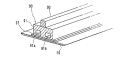
図5は、電極の他の変形態様を示したものである。
この電極90は、上側の第1金属部材91と、下側の第2金属部材92とに分かれている。第1金属部材91と第2金属部材92は、単に上下に重ねられているだけであり、ボルトや溶接等の固定手段で接合、固定されてはいない。
FIG. 5 shows another modification of the electrode.
The
第1金属部材91は、第1実施形態の電極30と同様の構造になっている。概説すると、第1金属部材91は、アルミやステンレス等の金属にて構成され、厚肉の平板状(断面四角形)をなして前後に長く延びている。第1金属部材91は、第2金属部材92より十分に大きな重量を有している。第1金属部材91の上面には金属リブ93が設けられている。第1金属部材91の内部には、冷却・温調構造として2条の通路91a,91bが形成されている。純正窒素ガス(冷却・温調媒体)が通路91aを往路とし、通路91bを復路として流通されることにより、第1金属部材91が内部から冷却・温調されるようになっている。
第1金属部材91の冷却・温調構造は、上記通路91a,91bに代えて、図4に示すような2本のパイプ81,82で構成されていてもよい。
The
The cooling / temperature adjustment structure of the
第2金属部材92は、第1金属部材91より少し幅広で、第1金属部材91より十分に薄い平板状をなし、前後に延びている。
第2金属部材92は、アルミニウムにて構成され、その厚さは、約2mmに設定されている。
The
The
この第2金属部材92が、固体誘電体板50の上に非固定状態で単に載置されている。この第2金属部材92の上に第1金属部材91が非固定状態で単に載置されている。
したがって、第2金属部材92が、自らの自重だけでなく第1金属部材91の重みによっても固体誘電体板50に押し当てられている。これにより、第2金属部材92の平らな下面全体を固体誘電体板50と面接触させることができる。第1金属部材91は、厚肉平板状であり、荷重を第2金属部材92のほぼ全体に均一にかけることができる。
The
Therefore, the
プラズマ放電時には第2金属部材92の下面(固体誘電体板50との当接面)が最も高温になる。第2金属部材92の材料であるアルミニウムは熱伝導が良好であるので、第2金属部材92の下面の熱は厚さ方向にすばやく伝わる。しかも、第2金属部材92の厚さは2mm程度であり極めて小さい。これにより、熱が第2金属部材92の上面に簡単に達することができる。したがって、プラズマ放電時には第2金属部材92の全体がほぼ均一に温度上昇することになり、第2金属部材92の厚さ方向の温度勾配が極めて小さく、第2金属部材92の上面と下面の温度差は僅か1℃程度以内にとどまる。しかも第2金属部材92は固体誘電体板50上に非固定状態で単に載置されているだけであり、固体誘電体板50から独立して単独で固体誘電体板50の上面に沿う水平方向に変位自在になっている。これによって、第2金属部材92は、主に長手方向にまっすぐ伸び変形することになり、撓み変形を来たさないようにでき、平らな形状を維持することができる。よって、第2金属部材92と固体誘電体板50の間に隙間が形成されるのを確実に防止でき、両者間にアーキングが発生するのを確実に防止することができる。
During plasma discharge, the lower surface of the second metal member 92 (the contact surface with the solid dielectric plate 50) is at the highest temperature. Since aluminum, which is the material of the
熱は第2金属部材92から第1金属部材91に伝達され、第1金属部材91も温度上昇することになる。このとき、第1金属部材91の内部に厚さ方向に温度勾配が形成され、第1金属部材91が撓む場合がある。しかし、第1金属部材91が固体誘電体板50と直接接しているわけではなく、しかも第1金属部材91は第2金属部材92から独立して撓み変形可能であるので、第2金属部材92に熱応力が伝達されることはない。したがって、電極90の第1金属部材91が撓み変形を来たしても、固体誘電体板50と電極90の間に隙間が形成されることはなく、両者間にアーキングが発生することはなく、何ら問題が無い。
The heat is transmitted from the
一方、第1金属部材91が撓んでも、第1金属部材91のどこか一箇所は必ず第2金属部材91と接触している。これによって、第1金属部材91と第2金属部材92の電気的導通状態を維持でき、第1金属部材91を介して第2金属部材92に確実に給電することができる。
On the other hand, even if the
第2金属部材92が第1金属部材91より少し幅方向に突出されるようになっているため、第1金属部材91の幅方向の端部からアークが飛ぶのを防止することができる。
プラズマ放電と併行して、通路91a,91bに純正窒素ガス(冷却・温調媒体)を通すことにより、第1金属部材91ひいては第2金属部材92を冷却・温調することができ、これら金属部材91,92の熱変形を抑制することができる。
Since the
In parallel with the plasma discharge, by passing pure nitrogen gas (cooling / temperature control medium) through the
第2金属部材92は、アルミニウムに限られずステンレス等の他の金属材料で構成してもよい。第2金属部材92の厚さは、材料の熱伝導度に応じて設定し、プラズマ放電時の加熱による上面と下面の温度差が略1℃以下になるような大きさにする。したがって、第2金属部材92としてアルミニウムより熱伝導度が小さい材料を用いる場合、厚さをより小さくする。例えばステンレスの場合、第2金属部材92の厚さはほぼ0.3〜0.5mmとする。
The
本発明は、上記実施形態に限定されるものではなく、種々の改変をなすことができる。
筐体本体21における処理通路12の下流側の外側面に、テフロン(登録商標)等からなる耐腐食性のコーティングを施すことにしてもよい。
セラミック製の固体誘電体50の破損を防止するとの観点からは、処理通路12の下流側の板支持部材62を金属にする一方、上流側の板支持部材61を固体誘電体50より軟質の樹脂等で構成してもよく、2つの部材61,62を共に固体誘電体50より軟質の樹脂等で構成してもよい。
金属製の板支持部材61は、筐体本体21と一体になっていてもよい。
電極の冷却・温調媒体として窒素以外の物質(例えば水、空気等)を用いることにしてもよい。
本発明は、エッチング、成膜、表面改質等の種々のプラズマ処理に適用でき、常圧プロセスに限らず、減圧プロセスにも適用できる。
The present invention is not limited to the above embodiment, and various modifications can be made.
A corrosion-resistant coating made of Teflon (registered trademark) or the like may be applied to the outer surface of the
From the viewpoint of preventing breakage of the ceramic
The metal
Substances other than nitrogen (for example, water, air, etc.) may be used as the electrode cooling / temperature control medium.
The present invention can be applied to various plasma treatments such as etching, film formation, and surface modification, and can be applied not only to a normal pressure process but also to a pressure reduction process.
本発明は、例えば半導体製造における基板のプラズマ表面処理に利用可能である。 The present invention can be used, for example, for plasma surface treatment of a substrate in semiconductor manufacturing.
M プラズマ処理装置
W 基板
10 処理ヘッド
10L,10R プラズマ処理部(処理ユニット)
11 プロセスガス導入路
12 処理通路
12a 放電空間
12b 処理通路における放電空間の上流側に連なる空間(処理通路の上流側部)
12c 処理通路における放電空間の下流側に連なる空間(処理通路の下流側部)
13,14 電極外空間
20 筐体
30 電極
31,32 電極内通路
46a 電極規制部
50 固体誘電体板
61 上流側の金属製板支持部材(上流部材)
61a 上流側の板支持部
62 下流側の樹脂製板支持部材(下流部材)
62a 下流側の板支持部
73a 窒素導入路
74a 窒素導出路
80 電極
81,82 電極内通路
90 電極
91 第1金属部材
91a,91b 電極内通路
92 第2金属部材
M Plasma processing
11 Process
12c Space connecting to the downstream side of the discharge space in the processing passage (downstream portion of the processing passage)
13, 14 Electrode
61a
62a Downstream
Claims (10)
前記プラズマ処理部が、底部が開放された筐体と、この筐体の底部を塞ぐように筐体に支持された固体誘電体の板と、前記筐体の内部に水平方向の少なくとも一方向へフリーになるようにして収容された電極とを備え、
前記固体誘電体板が、単独で前記電極の自重を支持可能な強度を有し、
前記電極が、前記固体誘電体板の上面に非固定状態で載置され、自重のほぼ全てを固体誘電体板に掛けていることを特徴とするプラズマ処理装置。 In a plasma processing apparatus having a plasma processing unit in which a substrate is disposed below and a process gas is to be introduced between the substrate and the substrate,
The plasma processing unit includes a casing whose bottom is open, a solid dielectric plate supported by the casing so as to close the bottom of the casing, and at least one horizontal direction inside the casing. With electrodes housed so as to be free,
The solid dielectric plate has a strength capable of supporting the weight of the electrode by itself;
The plasma processing apparatus, wherein the electrode is mounted in an unfixed state on the upper surface of the solid dielectric plate, and substantially all of its own weight is hung on the solid dielectric plate.
前記筐体には、固体誘電体板の幅方向の両端部を長手方向に変位可能に支持する一対の板支持部が設けられていることを特徴とする請求項2又は3に記載のプラズマ処理装置。 The solid dielectric plate extends in the same direction as the electrode;
4. The plasma processing according to claim 2, wherein the casing is provided with a pair of plate support portions that support both ends in the width direction of the solid dielectric plate so as to be displaceable in the longitudinal direction. 5. apparatus.
前記筐体には、前記固体誘電体板の幅方向の両端部を支持する一対の板支持部が設けられ、各板支持部が、上向きの斜面をなして前記固体誘電体板の下向き斜面と当接する板支持面を有していることを特徴とする請求項2又は3に記載のプラズマ処理装置。 The solid dielectric plate extends in the same direction as the electrode, and both end faces in the width direction are downward slopes,
The casing is provided with a pair of plate support portions that support both ends in the width direction of the solid dielectric plate, and each plate support portion forms an upward slope and a downward slope of the solid dielectric plate. The plasma processing apparatus according to claim 2, further comprising a plate support surface that abuts.
前記一対の板支持部のうち一方が、樹脂にて構成され、他方の板支持部が、金属にて構成されていることを特徴とする請求項4又は5に記載のプラズマ処理装置。 The solid dielectric plate is made of ceramic;
6. The plasma processing apparatus according to claim 4, wherein one of the pair of plate support portions is made of a resin, and the other plate support portion is made of a metal.
前記固体誘電体板の上に前記第2金属部材が非固定状態で載置され、この第2金属部材の上に前記第1金属部材が非固定状態で載置されており、
第2金属部材の上面と下面のプラズマ放電時の温度差が所定以下になるように、第2金属部材の材料及び厚さが設定されていることを特徴とする請求項1に記載のプラズマ処理装置。 The electrode is divided into a first metal member and a second metal member, the first metal member is heavier than the second metal member, and the second metal member has a thin plate shape,
The second metal member is placed in an unfixed state on the solid dielectric plate, and the first metal member is placed in an unfixed state on the second metal member,
2. The plasma processing according to claim 1, wherein the material and thickness of the second metal member are set so that a temperature difference during plasma discharge between the upper surface and the lower surface of the second metal member becomes a predetermined value or less. apparatus.
Priority Applications (13)
| Application Number | Priority Date | Filing Date | Title |
|---|---|---|---|
| JP2005240542A JP3858043B2 (en) | 2004-09-29 | 2005-08-23 | Plasma processing equipment |
| PCT/JP2005/017251 WO2006035628A1 (en) | 2004-09-29 | 2005-09-20 | Plasma processing system |
| EP05785311A EP1796442B1 (en) | 2004-09-29 | 2005-09-20 | Plasma processing system |
| KR1020077009447A KR101020411B1 (en) | 2004-09-29 | 2005-09-20 | Plasma processing system |
| US11/664,133 US7886689B2 (en) | 2004-09-29 | 2005-09-20 | Plasma processing apparatus |
| CN2005800318920A CN101023714B (en) | 2004-09-29 | 2005-09-20 | Plasma processing apparatus |
| US11/663,983 US7886688B2 (en) | 2004-09-29 | 2005-09-20 | Plasma processing apparatus |
| DE602005024702T DE602005024702D1 (en) | 2004-09-29 | 2005-09-20 | PLASMA PROCESSING SYSTEM |
| KR1020077009562A KR101020463B1 (en) | 2004-09-29 | 2005-09-20 | Plasma processing apparatus |
| PCT/JP2005/017252 WO2006035629A1 (en) | 2004-09-29 | 2005-09-20 | Plasma processing apparatus |
| CN2005800318901A CN101023713B (en) | 2004-09-29 | 2005-09-20 | Plasma processing apparatus |
| TW094132660A TW200623972A (en) | 2004-09-29 | 2005-09-21 | Plasma treatment device |
| TW094132666A TWI291203B (en) | 2004-09-29 | 2005-09-21 | Plasma processing apparatus |
Applications Claiming Priority (2)
| Application Number | Priority Date | Filing Date | Title |
|---|---|---|---|
| JP2004285506 | 2004-09-29 | ||
| JP2005240542A JP3858043B2 (en) | 2004-09-29 | 2005-08-23 | Plasma processing equipment |
Publications (3)
| Publication Number | Publication Date |
|---|---|
| JP2006128078A JP2006128078A (en) | 2006-05-18 |
| JP2006128078A5 JP2006128078A5 (en) | 2006-07-27 |
| JP3858043B2 true JP3858043B2 (en) | 2006-12-13 |
Family
ID=36722547
Family Applications (1)
| Application Number | Title | Priority Date | Filing Date |
|---|---|---|---|
| JP2005240542A Expired - Fee Related JP3858043B2 (en) | 2004-09-29 | 2005-08-23 | Plasma processing equipment |
Country Status (1)
| Country | Link |
|---|---|
| JP (1) | JP3858043B2 (en) |
Families Citing this family (3)
| Publication number | Priority date | Publication date | Assignee | Title |
|---|---|---|---|---|
| JP2007250426A (en) * | 2006-03-17 | 2007-09-27 | Sharp Corp | Electrode structure of plasma processing system and plasma processing system provided with the same |
| JP4820241B2 (en) * | 2006-08-29 | 2011-11-24 | 株式会社ケーヒン | Wiring board storage structure |
| JP2008153065A (en) * | 2006-12-18 | 2008-07-03 | Sekisui Chem Co Ltd | Plasma treatment device |
-
2005
- 2005-08-23 JP JP2005240542A patent/JP3858043B2/en not_active Expired - Fee Related
Also Published As
| Publication number | Publication date |
|---|---|
| JP2006128078A (en) | 2006-05-18 |
Similar Documents
| Publication | Publication Date | Title |
|---|---|---|
| KR101020411B1 (en) | Plasma processing system | |
| JP4584722B2 (en) | Plasma processing apparatus and semiconductor device manufactured by the same | |
| US20150159958A1 (en) | High-efficiency heat exchanger and high-efficiency heat exchange method | |
| US20080055855A1 (en) | Heat sink for electronic components | |
| JP7260681B2 (en) | Organic film forming device | |
| JP3858043B2 (en) | Plasma processing equipment | |
| US9842746B2 (en) | Purge gas spraying plate and fume removing apparatus having the same | |
| KR101314723B1 (en) | Heat exchanger for process cooling system | |
| JP5653950B2 (en) | Cooling system | |
| JP4326300B2 (en) | Plasma CVD apparatus and electrode for plasma CVD apparatus | |
| JP4499005B2 (en) | Plasma processing equipment | |
| JP5333161B2 (en) | heatsink | |
| JP5406848B2 (en) | Atmospheric pressure plasma processing equipment | |
| KR20220051236A (en) | THERMALLY CONTROLLED Chandelier Showerhead | |
| JP2007080688A (en) | Electrode structure for plasma treatment apparatus | |
| JP2006128081A (en) | Plasma treatment device | |
| JP4786723B2 (en) | Plasma CVD apparatus and electrode for plasma CVD apparatus | |
| KR101327573B1 (en) | In line heater assembly | |
| US7177152B1 (en) | Collective and restrictive inhalant and radiating device for appliances | |
| JP4800845B2 (en) | Plasma processing equipment | |
| JP5028459B2 (en) | Plasma processing equipment | |
| JP7470558B2 (en) | heat sink | |
| KR101670381B1 (en) | Heater of apparatus for removing fume and apparatus for removing fume using the same | |
| JP5331582B2 (en) | Heating device with cooling function | |
| US9236211B2 (en) | Electrode for dielectric barrier discharge treatment of a substrate |
Legal Events
| Date | Code | Title | Description |
|---|---|---|---|
| A521 | Written amendment |
Free format text: JAPANESE INTERMEDIATE CODE: A523 Effective date: 20060609 |
|
| A871 | Explanation of circumstances concerning accelerated examination |
Free format text: JAPANESE INTERMEDIATE CODE: A871 Effective date: 20060609 |
|
| TRDD | Decision of grant or rejection written | ||
| A975 | Report on accelerated examination |
Free format text: JAPANESE INTERMEDIATE CODE: A971005 Effective date: 20060808 |
|
| A01 | Written decision to grant a patent or to grant a registration (utility model) |
Free format text: JAPANESE INTERMEDIATE CODE: A01 Effective date: 20060822 |
|
| A61 | First payment of annual fees (during grant procedure) |
Free format text: JAPANESE INTERMEDIATE CODE: A61 Effective date: 20060915 |
|
| FPAY | Renewal fee payment (prs date is renewal date of database) |
Free format text: PAYMENT UNTIL: 20090922 Year of fee payment: 3 |
|
| FPAY | Renewal fee payment (prs date is renewal date of database) |
Free format text: PAYMENT UNTIL: 20100922 Year of fee payment: 4 |
|
| FPAY | Renewal fee payment (prs date is renewal date of database) |
Free format text: PAYMENT UNTIL: 20110922 Year of fee payment: 5 |
|
| FPAY | Renewal fee payment (prs date is renewal date of database) |
Free format text: PAYMENT UNTIL: 20120922 Year of fee payment: 6 |
|
| FPAY | Renewal fee payment (prs date is renewal date of database) |
Free format text: PAYMENT UNTIL: 20130922 Year of fee payment: 7 |
|
| LAPS | Cancellation because of no payment of annual fees |