JP3761289B2 - Dielectric material, manufacturing method thereof, circuit board using the same, and multilayer circuit board - Google Patents
Dielectric material, manufacturing method thereof, circuit board using the same, and multilayer circuit board Download PDFInfo
- Publication number
- JP3761289B2 JP3761289B2 JP18456797A JP18456797A JP3761289B2 JP 3761289 B2 JP3761289 B2 JP 3761289B2 JP 18456797 A JP18456797 A JP 18456797A JP 18456797 A JP18456797 A JP 18456797A JP 3761289 B2 JP3761289 B2 JP 3761289B2
- Authority
- JP
- Japan
- Prior art keywords
- dielectric material
- strontium
- weight
- tio
- material according
- Prior art date
- Legal status (The legal status is an assumption and is not a legal conclusion. Google has not performed a legal analysis and makes no representation as to the accuracy of the status listed.)
- Expired - Fee Related
Links
Images

Classifications
-
- H—ELECTRICITY
- H01—ELECTRIC ELEMENTS
- H01P—WAVEGUIDES; RESONATORS, LINES, OR OTHER DEVICES OF THE WAVEGUIDE TYPE
- H01P7/00—Resonators of the waveguide type
- H01P7/08—Strip line resonators
- H01P7/082—Microstripline resonators
-
- C—CHEMISTRY; METALLURGY
- C03—GLASS; MINERAL OR SLAG WOOL
- C03C—CHEMICAL COMPOSITION OF GLASSES, GLAZES OR VITREOUS ENAMELS; SURFACE TREATMENT OF GLASS; SURFACE TREATMENT OF FIBRES OR FILAMENTS MADE FROM GLASS, MINERALS OR SLAGS; JOINING GLASS TO GLASS OR OTHER MATERIALS
- C03C10/00—Devitrified glass ceramics, i.e. glass ceramics having a crystalline phase dispersed in a glassy phase and constituting at least 50% by weight of the total composition
- C03C10/0036—Devitrified glass ceramics, i.e. glass ceramics having a crystalline phase dispersed in a glassy phase and constituting at least 50% by weight of the total composition containing SiO2, Al2O3 and a divalent metal oxide as main constituents
- C03C10/0045—Devitrified glass ceramics, i.e. glass ceramics having a crystalline phase dispersed in a glassy phase and constituting at least 50% by weight of the total composition containing SiO2, Al2O3 and a divalent metal oxide as main constituents containing SiO2, Al2O3 and MgO as main constituents
-
- H—ELECTRICITY
- H01—ELECTRIC ELEMENTS
- H01P—WAVEGUIDES; RESONATORS, LINES, OR OTHER DEVICES OF THE WAVEGUIDE TYPE
- H01P7/00—Resonators of the waveguide type
- H01P7/08—Strip line resonators
- H01P7/084—Triplate line resonators
-
- H—ELECTRICITY
- H05—ELECTRIC TECHNIQUES NOT OTHERWISE PROVIDED FOR
- H05K—PRINTED CIRCUITS; CASINGS OR CONSTRUCTIONAL DETAILS OF ELECTRIC APPARATUS; MANUFACTURE OF ASSEMBLAGES OF ELECTRICAL COMPONENTS
- H05K1/00—Printed circuits
- H05K1/02—Details
- H05K1/03—Use of materials for the substrate
- H05K1/0306—Inorganic insulating substrates, e.g. ceramic, glass
Landscapes
- Chemical & Material Sciences (AREA)
- Engineering & Computer Science (AREA)
- Ceramic Engineering (AREA)
- Crystallography & Structural Chemistry (AREA)
- Dispersion Chemistry (AREA)
- Life Sciences & Earth Sciences (AREA)
- Chemical Kinetics & Catalysis (AREA)
- General Chemical & Material Sciences (AREA)
- Geochemistry & Mineralogy (AREA)
- Materials Engineering (AREA)
- Organic Chemistry (AREA)
- Compositions Of Oxide Ceramics (AREA)
- Inorganic Insulating Materials (AREA)
- Glass Compositions (AREA)
- Production Of Multi-Layered Print Wiring Board (AREA)
Description
【0001】
【発明の属する技術分野】
本発明は、マイクロ波領域での誘電特性に優れた誘電体材料及びその製造方法に関する。また、本発明は、この誘電体材料からなる基板の表面或いは積層された基板の間に、金、銀及び銅等の導体材料からなる配線パターンを形成し、特に同時焼成して得られる回路基板及び多層回路基板に関する。本発明の誘電体材料は、このような回路基板等としてマイクロ波領域における誘電体共振器、フィルタなどとして使用することができる。
【0002】
【従来の技術】
Al2 O3 、TiO2 等の無機フィラーとガラス成分とからなる絶縁体層を用いて、900℃前後の低温において焼成することにより得られる多層回路基板が既に使用されている。この多層回路基板は、未焼成の基板に金、銀及び銅等の導電率の高い導体材料を印刷した後、積層し、低温において同時焼成することにより得られ、導体を内部電極とした積層型の誘電体共振器或いはフィルタ等として使用されている。
【0003】
このような多層回路基板等を構成する誘電体材料には、
▲1▼共振周波数の温度係数(以下、τf と表す。)の絶対値が小さいこと、
▲2▼マイクロ波領域での無負荷品質係数(以下、Qu と表す。)が大きいこと、
を同時に満たすことが要求される。
【0004】
上記の絶縁体層を形成するガラス成分としては、硼珪酸塩系やアルミノ珪酸塩系のガラス等が用いられる。しかし、これらのガラス成分及びこれらのガラス成分に無機フィラーとしてAl2 O3 を添加した基板材料では、τf が負の大きな値であるため温度によって共振周波数が大きく変動する。そのため、共振器或いはフィルタを作製するための基板材料としては好ましくない。そこで、このような基板材料のτf を補正するために、例えばTiO2 、CaTiO3 及びSrTiO3 等の、大きな正のτf を有する無機フィラーを添加する手法が提案されている。
【0005】
【発明が解決しようとする課題】
しかしながら、これらの無機フィラーは、ガラス成分或いはこれにAl2 O3 を添加した誘電体材料及び配線パターン、厚膜抵抗体皮膜等と反応し易く、誘電体材料からなる基板表面の厚膜抵抗体皮膜等の特性を変化させてしまうことがある。また、反応によりガラス成分と固溶し、無機フィラーの結晶構造が乱れ、期待されるτf の補正効果が得られないという問題がある。更に、上記の無機フィラーを多量に添加したり、粒径の大きい無機フィラーを添加すると、均質な誘電体材料を得ることが難しく、且つ低温において焼成した場合に、焼結体の緻密化が困難となる。一方、低温において焼成される誘電体材料のQu の向上については、有効な手段が提案されていないのが実状であり、現用品の無負荷品質係数と共振周波数との積は高々1000GHz程度である。
【0006】
本発明は、上記問題点を解決するものであり、特にτf の絶対値が20以下と小さく、且つQu と共振周波数(以下、f0 と表す。)との積Qu ×f0 が1800GHz以上、更には2500GHz以上と大きく、特に低温で焼成した場合であっても均質で緻密な焼結体を得ることができる誘電体材料及びその製造方法並びにそれを用いた回路基板及び多層回路基板を提供することを目的とする。
【0007】
【課題を解決するための手段】
第1発明の誘電体材料は、ストロンチウムアノーサイト(SrAl2Si2O8)を主結晶相とし、他の結晶相としてTiO 2 を含み、該TiO 2 の含有量は0.5〜4.5重量%であるガラスセラミックスからなることを特徴とする。
【0008】
更に、第2発明の誘電体材料は、主結晶相としてストロンチウムアノーサイト(SrAl2Si2O8)を含む結晶化ガラス99.5〜95.5重量%と、TiO20.5〜4.5重量%とからなることを特徴とする。また、第4発明の誘電体材料は、結晶相としてチタン酸ストロンチウムを含まない結晶化ガラスとTiO2とからなり、該結晶化ガラスは、ストロンチウムアノーサイト(SrAl2Si2O8)及びチタン酸マグネシウム(MgTi2O5)を結晶相として含み、上記結晶化ガラスは99.5〜95.5重量%であり、上記TiO2は0.5〜4.5重量%であることを特徴とする。
【0009】
本発明において上記「ストロンチウムアノーサイト」(SrAl2 Si2 O8 、以下Srアノーサイトという。)とは、長石、即ちアノーサイト(CaAl2 Si2 O8 )のCaがSrに置き換わったものである。また、上記「主結晶相」とは、焼成後、焼結体を粉砕し、粉末X線回折法によって結晶相を同定した場合に、最強の積分強度を与える結晶相と定義する。尚、第4発明においても、Srアノーサイトが、この定義による主結晶相となっている。
【0010】
第1発明において、上記「ガラスセラミックス」は、ガラスと無機フィラーからなる結晶粒との混合物を焼成して得られる複合体であり、第1発明では、無機フィラーとしてストロンチウム化合物(以下、Sr化合物という。)の他に特にTiO2が使用される。また、第2及び4発明における上記「結晶化ガラス」は、非晶質相と結晶相とからなり、主たる結晶相として上記のSrアノーサイトを含んでいる。尚、Srアノーサイトは、第6発明のように、ガラスフリットと無機フィラーであるSr化合物との反応によって生成する。また、予め合成したSrアノーサイトをガラスフリットに添加し、混合することもできる。
【0011】
この主結晶相であるSrアノーサイトは、τf を正の方向に補正する作用を有し、且つQu を向上させる効果が大きい。但し、Sr化合物としてチタン酸ストロンチウムを使用した場合、Srアノーサイトとともに生成するチタン酸マグネシウム(MgTi2 O5 )は負のτf を有する。そのため、チタン酸ストロンチウムの添加量が約25重量%以上では、誘電体材料のτf は却って負の側へシフトする。本発明では、このτf の負の側へのシフトを抑え、その絶対値を更に0に近づけるため、適量の正のτf を有する無機フィラー、特にTiO2 を併用するものである。
【0012】
上記のSrアノーサイトが、第5発明のように、母相である結晶化ガラスを100重量%とした場合に、40重量%以上含有されていればQu が十分に向上する。また、第9発明のように、Srアノーサイトが、本発明の誘電体材料中の各結晶相の合計量を100重量%とした場合に、50〜85重量%であれば実用上十分なQu を有する誘電体材料を得ることができる。この第9発明においても、Srアノーサイトが、母相である結晶ガラスを100重量%とした場合に、40重量%以上含有されておれば、Qu がより大きく向上するため好ましい。
【0013】
更に、第1及び2発明の誘電体材料では、Sr化合物として各種のものを使用し得るが、生成するストロンチウム元素を含む結晶相は、第8発明のように、実質的にSrアノーサイトのみである。これは使用されるSr化合物がそのまま結晶相として残留することなく、その多くがガラス成分と反応してSrアノーサイトに変化していることを意味している。これはSr化合物として特にチタン酸ストロンチウム又はスズ酸ストロンチウムを使用する第13発明の製造方法により得られる誘電体材料においても同様である。この誘電体材料においても、使用したチタン酸ストロンチウム又はスズ酸ストロンチウムがそのまま結晶相として残留することはなく、また、Srアノーサイト以外のストロンチウム元素を含む結晶相は確認されない。
【0014】
尚、用いるSr化合物の粒径によって、得られる誘電体材料のτf 及びQu の挙動が異なる。Sr化合物の粒径が小さい場合は、この化合物の多くがガラス成分と反応し、Srアノーサイトが生成してQu が向上する。但し、Sr化合物がチタン酸ストロンチウムである場合は、同時に生成するMgTi2 O5 のため、τf は第7発明の下限である「−20ppm/℃」以上にまでは補正されず、適量のTiO2 によってτf を更に正の側へ補正することになる。
【0015】
一方、チタン酸ストロンチウムの粒径が大きい場合は、この化合物からSrアノーサイトへの反応が十分に進まず、同時にMgTi2 O5 の生成量も少ない。そして、多量に残存するチタン酸ストロンチウムのτf を正の側へ補正する作用によって、τf は第7発明の上限である「+20ppm/℃」を越えて正の側へシフトするため好ましくない。また、主結晶相がSrアノーサイトとならないため、Qu もそれほど向上しない。尚、Sr化合物としてスズ酸ストロンチウムを使用した場合は、MgTi2 O5 は生成せず、τf の挙動は異なったものとなるが、チタン酸ストロンチウムを使用した場合と同様に優れたτf 及びQu ×f0 を有する誘電体材料を得ることができる。しかし、εr はやや低くなる。
【0016】
上記「TiO2 」は特定の結晶系に限定されず、一般的な結晶系であるルチル型等、いずれも使用することができ、焼成後も添加時の結晶系のまま残る。このTiO2 はτf を正の方向に大きく補正する作用を有し、且つ比誘電率(εr )を向上させる。このTiO2 が0.5重量%未満である場合は、τf を−20ppm/℃を越えて、更に正の側へ補正することができないことがあり、εr も十分に向上しない場合がある。また、TiO2 が4.5重量%を越える場合は、τf が+20ppm/℃を越えて大きくなってしまう傾向にある。このTiO2 の含有量は特に1.0〜4.0重量%であることが好ましく、この範囲の含有量とすれば、τf を−10〜+10ppm/℃程度にすることができる。更に、TiO2 の含有量は1.2〜3.5重量%であることがより好ましく、この範囲の含有量とすれば、τf を−5〜+5ppm/℃程度にすることができる。
【0017】
TiO2の添加量はQuには特に影響を与えず、第2及び4発明に特定されるTiO2の含有量の範囲において、Qu×f0は1800GHz以上、特に2500GHzを越える値とすることができ何ら問題はない。尚、第1発明においても、TiO2の含有量は上記の特定の範囲とすることが好ましい。また、本発明において、QuはSr化合物の使用量及び焼成温度等、によって影響を受けるが、通常、Qu×f0は2000GHz以上とすることができる。このQu×f0は特に2500GHz以上であることが好ましく、更には後記の実施例のように2900GHz以上或いは3000GHzを越える高い値とすることができ、本発明では、非常に優れた性能の誘電体材料を得ることができる。
【0018】
第10発明の誘電体材料の製造方法は、ガラスフリットとSr化合物との混合物99.5〜95.5重量%と、TiO2 0.5〜4.5重量%とを混合し、成形した後、850〜1000℃で焼成し、吸水率が0.1%未満となるまで緻密化させるとともに、上記ガラスフリットと上記Sr化合物とを反応せしめ、主結晶相としてSrアノーサイト(SrAl2 Si2 O8 )を生成させることを特徴とする。尚、予め合成したSrアノーサイトを、無機フィラーとしてTiO2 とともにガラスフリットに添加し、混合することもできる。しかし、この第10発明のように、焼成過程においてガラスフリットとSr化合物とを反応させ、Srアノーサイトを生成せさたほうが工程数が少なく、工業的に有利である。
【0019】
上記「ガラスフリット」の組成は特に限定されないが、第11発明のように、このガラスフリットを100重量%とした場合に、40〜52重量%のSiO2 、27〜37重量%のAl2 O3 、11〜13重量%のMgO、2〜8重量%のB2 O3 、2〜8重量%のCaO及び0.1〜3重量%のZrO2 からなるものが好ましい。このような組成のガラスフリットであれば、850〜1000℃の比較的低い焼成温度で、焼結させ、結晶化させることができ、吸水率が「0.1%未満」となるまで「緻密化」することができる。また、誘電体材料の抗折強度も150MPa以上と実用的な強度を持つ良品を得ることができる。
【0020】
また、このガラスフリットの組成は、第12発明のように、ガラスフリットを100重量%とした場合に、40〜52重量%のSiO2 、27〜37重量%のAl2 O3 、11〜13重量%のMgO、2〜8重量%のB2 O3 及び2〜8重量%のCaOからなるものとすることもできる。このような組成のガラスフリットであっても、同様に比較的低い焼成温度で、焼結させ、結晶化させることができ、十分に緻密化することができる。更に、抗折強度も同様に150MPa以上と実用的な強度を持つ良品とすることができる。また、このガラスフリットには、結晶核を形成する作用を有すると考えられるZrO2 に代えて、他の公知の核形成剤を添加することもできる。
【0021】
上記「Sr化合物」としては、ガラスフリットと反応してSrアノーサイトが生成するものであれば、特に制限されることなく使用することができる。このSr化合物の一部はガラス相に固溶するかもしれないが、それを除いた実質的に全量がSrアノーサイトに変化することが好ましい。また、Sr化合物としては、第13発明の、SrTiO3 、Sr3 Ti2 O7 、Sr2 TiO4 及びSrSnO3 が好適である。
【0022】
また、これらSr化合物は、通常、粉末状であるが、その平均粒径が小さく、比表面積が大きいものを使用すれば、ガラスフリットとSr化合物とが容易に反応するため好ましい。その平均粒径は特定されないが、5μm以下、特に3μm以下、更には第14発明のように、2μm以下であるものが好ましい。この平均粒径が5μmを越える場合は、Sr化合物のSrアノーサイトへの変化が十分に進まず、使用したSr化合物からなる結晶相が、作製した誘電体材料中の主結晶相となってしまう傾向にある。その場合、τf が正の方向へ非常に大きくなってしまい好ましくない。
【0023】
尚、ガラスフリットとSr化合物との混合比は特に限定されないが、第15発明のように、ガラスフリットに含有されるSiO2 のSiのモル数と、Al2 O3 のAlのモル数のうちの少ない方のモル数が、Sr化合物のSrのモル数の2倍を越える場合は、使用するSr化合物のすべてが理論上Srアノーサイトに変化するため好ましい。このように理論上とするのは、焼成条件等が変わった場合に、添加するSr化合物のすべてがSrアノーサイトに変化しないこともあり得るからである。しかし、その場合でも、残留するSr化合物が特に悪影響を及ぼさず、τf が−20〜+20ppm/℃であり、且つQu ×f0 が1800GHz以上であれば、実用上問題はなく本発明の誘電体材料を得ることができる。
【0024】
また、例えばSr化合物としてSrTiO3 を用いた場合、第4発明の誘電体材料のように、Srアノーサイトの他、MgTi2 O5 等の結晶相が生成し、結晶化ガラス中に存在する。しかし、結晶化ガラス中の主結晶相がSrアノーサイトであり、他の結晶相が特に誘電特性に悪影響を及ぼさず、τf が−20〜+20ppm/℃であり、且つQu ×f0 が1800GHz以上であれば、実用上問題はなく本発明の誘電体材料を得ることができる。
【0025】
本発明の誘電体材料は比較的低温で焼成することができ、この誘電体材料からなる基板と金、銀、銅等の導体材料からなる配線パターン等とを同時焼成することができる。上記「焼成」の温度が850℃未満では、ガラスフリットとSr化合物との反応が十分に進まず、Sr化合物のSrアノーサイトへの変化が生じ難い。そのため、τf が正の側に大きくなってしまい、且つQu も十分に向上しない。また、誘電体材料を十分に緻密化し、その吸水率を0.1%未満とすることもできない。
【0026】
更に、焼成温度が「1000℃」を越えると、導体材料と同時焼成する場合に、誘電体材料と導体材料との反応、誘電体材料への導体材料の固溶、或いは導体材料の融解、拡散及び揮発等が起こることがある。そのため、配線パターンを作製する上で問題を生じ易く、且つ他の結晶が析出してSrアノーサイトが主結晶相とならないことがある。
【0027】
上記の焼成温度は880℃以上、特に900℃以上、更には930℃以上とすることが好ましい。焼成温度が900℃未満、特に880℃未満ではSr化合物が未反応のまま残留することもあり、その場合はτf が正の側に大きくなりすぎ、Qu も十分に向上しない。また、930℃以上の焼成温度では、τf 及びQu にはそれほど大きな変化はみられず、これは930℃程度でSr化合物からSrアノーサイトへの反応が終わるためではないかと考えられる。このことから焼成温度は930〜950℃とするのが最も効果的であるといえる。
【0028】
第1乃至9発明の誘電体材料及び第10発明の方法により製造される誘電体材料は、第16発明のように、この誘電体材料からなる基板の表面に導体材料からなる配線パターンを形成し、回路基板とすることができる。また、第17発明のように、これら基板を積層するとともに、少なくともこの積層された基板の間に導体材料からなる内部配線パターンを形成し、多層回路基板とすることができる。これら基板はマイクロ波領域における共振器或いはフィルタなどとして使用することができる。
【0029】
【発明の実施の形態】
以下、実施例により本発明を具体的に説明する。
実験例1〜14
表1に示す量比のガラス成分の各粉末を混合した後、1500℃の温度で2時間溶融し、その後、水中に投入してガラスを得た。次いで、このガラスを湿式粉砕した後、乾燥し、平均粒径約1μmのガラス粉末を得た。このガラス粉末に、表1に示す組み合わせ及び量比で、それぞれ表1に示す粒径のSr化合物と、平均粒径1.9μmのTiO2 とを加えた。これら各粉末をエタノール中において混合し、乾燥した後、成形助剤として樹脂成分(エチルメタアクリレート)を加えて造粒し、この造粒粉を8GPaの圧力下、直径23mm、厚さ12mmの円柱状に成形した。尚、実験例14においてはTiO2 に替えて平均粒径1μmのAl2 O3 を用いた。
【0030】
次に、上記の円柱状の成形体を15GPaの圧力下、等方静水圧プレス(CIP)処理を行い、その後、このCIP処理後の成形体を大気雰囲気下、930℃と比較的低温において0.5時間焼成した。このようにして得られた誘電体材料を研磨した後、平行導体板型誘電体共振器法により、測定周波数5〜8GHzにおいて比誘電率(εr )、Qu 及びτf (温度範囲:25〜80℃)を測定した。また、主結晶相は、誘電特性の測定に用いた試片を粉砕し、粉末X線回折法によって確認した。結果を表1に併記する。
【0031】
尚、表1において誘電損失に関する特性の結果はQu ×f0 で表した。f0 はQu を測定する際の共振周波数であるが、Qu の測定毎に多少の変動がある。そのため、このQu とf0 との積による表現がより正確に誘電損失を表すものである。また、JIS C2141に準じて得られた誘電体材料の吸水率を測定したところ、実験例1〜14いずれも0.1%未満であった。
【0032】
【表1】

表1の結果によれば、65.6〜79.0重量%のガラス成分と、31.5〜18.0重量%のSr化合物を使用し、これに0.6〜4.5重量%のTiO2を組み合わせた実験例1〜7では、τfが−18.4〜+11.3ppm/℃、Sr化合物としてSrTiO3を用いた場合のQu×foが2840〜3200GHz、Sr化合物としてSrSnO3を用いた場合のQu×foが2320GHzと、非常に優れた誘電特性を有する誘電体材料が得られていることが分かる。これらの実験例では、チタン酸ストロンヂウム及びスズ酸ストロンチウムはそのまま残留してはおらず、生成したSrアノーサイトによってQu×foが大きく向上するとともに、TiO2のτfを正の側へ補正する作用によって、τfが上記の好ましい範囲に補正されるものと考えられる。また、結晶核形成の作用を有すると考えられるZrO2が添加されていないガラスフリットを用いた実験例8においては、Sr化合物としてチタン酸塩を用いた他の実験例1、2及び4〜7に比べてQu×foがやや低い。しかし、ほぼ同等の優れた誘電特性を有する誘電体材料が得られている。
【0034】
τf はTiO2 が0.6重量%と少ない実験例1の−18.2ppm/℃から、4.5重量%と上限である実験例5の+11.3ppm/℃の間の値となっている。特にTiO2 の量比が3.0重量%及び4.0重量%では、その絶対値は10.0ppm/℃以下である。更に、Sr化合物がSrTiO3 で且つTiO2 の量比が1.5重量%及び2.7重量%では、その絶対値は5.0ppm/℃以下であり、非常に優れた性能の誘電体材料が得られることが分かる。このように各実験例の誘電特性はそれぞれに異なるが、εr 、Qu ×f0 及びτf のバランスからみた総合的な特性では実験例2の誘電体材料が特に優れている。また、Sr化合物としてSrSnO3 を用いて誘電体材料を得た実験例3では、τf が負の側へシフトするが、同様に優れた性能の誘電体材料が得られた。
【0035】
尚、図1には、この実験例2の誘電体材料についての焼成前後のX線回折の結果を比較して示す。図1によれば、焼成前には回折ピークはSrTiO3 とTiO2 のピークのみである。しかし、焼成後はSrTiO3 のピークは観察されず、主たる回折ピークはSrAl2 Si2 O8 となり、MgTi2 O5 が生成していることも分かる。また、TiO2 の回折ピークは変化せず、TiO2 が焼成後もそのまま残っていることを確認することができる。
【0036】
一方、無機フィラーとしてTiO2 を併用しなかった実験例9では、τf の正の側への補正が十分になされず、負の側に大きいままとなっていることが分かる。また、同様にTiO2 を用いなかった実験例10では、SrTiO3 の粒径が9.8μmと大きいため、Srアノーサイトへの変化が進まず、主結晶相がSrTiO3 となっている。そのため、Qu ×f0 の向上が小さく、τf は正の側に非常に大きくなっている。この実験例10において、SrTiO3 の添加量を5.0重量%に減量した実験例11では、実験例10と同様にSrTiO3 が主結晶相として残っている。しかし、添加量そのものが少ないためτf は適度に補正されて優れた値となっている。しかし、Qu ×f0 は更に低下し、第7発明の下限を下回っている。
【0037】
更に、TiO2を上限を越え、5.4重量%使用した実験例12では、SrアノーサイトによるQu×f0の向上がやや不十分であり、τfも+20ppm/℃を少し越えて大きくなっていることが分かる。また、このTiO2の添加量を上限を大きく越えて使用した実験例13では、Qu×f0はより低下し、τfも正の側へ大きくなってしまっている。また、Sr化合物以外の無機フィラーとしてAl2O3を用いた実験例14では、εrも小さく、τfも負の側に大きいままとなっていることが分かる。
【0038】
実験例15〜18
表1の各実験例の中で特に優れた誘電特性を有する実験例2と同じ組成、量比の原料を用い、表2に示す焼成温度で焼成した以外はすべて実験例2と同様にして誘電体材料を製造した。この誘電体材料を用いて実験例2と同様にして、その誘電特性を評価し、主結晶相を確認した。結果を表2に示す。尚、誘電損失が非常に大きく共振波形が得られなかった実験例18では、表中に測定不能と表記した。
【0039】
【表2】
表2の結果によれば、焼成温度がそれぞれ900℃及び950℃である実験例15、16では、吸水率はいずれも0.1%未満であり、τf はそれぞれ+15.2ppm/℃及び+1.9ppm/℃、Qu ×f0 はそれぞれ2510GHz及び3010GHzであって、優れた性能の誘電体材料であることが分かる。これらの数値と、焼成温度が930℃である実験例2の結果と比べてみると、焼成温度が950℃の場合のτf の絶対値と実験例2のそれとが近似しており、焼成温度が低い900℃の場合は、残留するSrTiO3 が多いためかτf の絶対値が相当に大きくなっている。一方、Qu ×f0 も、焼成温度が950℃の場合と実験例2とが近似しており、焼成温度が900℃の場合は、Srアノーサイトの生成が不十分であるためかQu ×f0 が低い。これらの結果は、第10発明において、焼成温度の特に好適な範囲は930〜950℃であることを裏付けるものである。
【0041】
一方、第10発明の下限を下回る低温において焼成した実験例17及び18では、SrTiO3 のSrアノーサイトへの変化が進まず、主結晶相がSrTiO3 であった。また、低温焼成であるため焼結も十分に進まず、緻密度が低く、そのため吸水率も第10発明の上限を越えてそれぞれ0.5%及び2.0%と高いことが分かる。尚、特に実験例18では誘電損失が非常に大きく、共振波形が得られなかった。
【0042】
実験例19
表1の実験例2と同じ組成の原料を用い、ガラス成分、Sr化合物及び添加物の各粉末を実験例2と同様に、エタノール中において混合し、乾燥させた。その後、この混合粉末にアクリル系バインダ(エチルメタアクリレート)、可塑剤(ジオクチルフタレート)、分散剤(マレイン酸系部分エステル型高分子材料)を加え、トルエン及びメチルエチルケトン系溶剤中において十分混合して、スラリーを調製した。次いで、このスラリーからドクターブレード法により、0.1〜1.2mmの所定厚さのグリーンテープを作製した。
【0043】
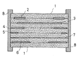
次に、厚膜回路成形用に使用される銀ペーストを用いて、上記範囲の各種厚さのグリーンテープ上に図2に示すような各種電極を形成するため、導体配線パターン(厚さ;20〜25μm)を印刷した。その後、これら導体パターンが印刷された複数のグリーンテープを所定の順に積層し、50℃の温度で、1GPaの圧力を加えて、積層物を一体化させた。次いで、この一体化させた積層物を250℃に加熱してバインダ等を分解除去した後、930℃、0.5時間保持の条件で焼成し、更に上下面及び側面にも銀/白金ペースト若しくは銀/パラジウムペーストを用いて外部電極等を形成し、図2に示す縦断面構造の多層回路基板を得た。尚、この多層回路基板の主結晶相は、別途、導体配線パターン等を印刷しない他は同様の条件で、積層し、焼成した積層物を粉砕し、粉末X線回折法によって確認した。その結果、実験例2の場合と同様にSrアノーサイトであることが分かった。
【0044】
【発明の効果】
本発明の誘電体材料は、τfの絶対値が小さく、Qu×f0が大きく、且つ緻密度が高い。また、特に低温において焼成することができるため、金、銀等の導体からなる配線パターンを形成した後、同時焼成することができる。特に第5〜9発明では、Qu×f0がより大きい誘電体材料を得ることができる。更に、第10発明によれば、特に第2及び4発明に特定された組成となるように調製された原料を、比較的低温において導体材料と同時焼成することにより、優れた誘電特性と高い緻密度とを併せ有する誘電体材料を製造することができる。特に第11〜15発明に特定された原料、組成である場合は、より優れた性能の誘電体材料を得ることができる。
【0045】
更に、第16及び17発明によれば、第1乃至9発明の誘電体材料を用いて、誘電特性に優れ、各種電子部品に使用することができる回路基板及び多層回路基板を得ることができる。この多層回路基板は、マイクロ波領域で使用する共振器、フィルタなどとして使用することができる。
【図面の簡単な説明】
【図1】実験例2の誘電体材料について、焼成前後のX線回折の結果を比較して示すチャートである。
【図2】実験例19で作製した多層回路基板の縦断面図である。
【符号の説明】
1;誘電体基板、2;トリミング用電極、3;グランド層、4;共振電極、5;出入力電極、6;極発生電極、7;コイル電極、8;外部電極。[0001]
BACKGROUND OF THE INVENTION
The present invention relates to a dielectric material having excellent dielectric characteristics in the microwave region and a method for manufacturing the same. The present invention also provides a circuit board obtained by forming a wiring pattern made of a conductive material such as gold, silver and copper between the surface of the substrate made of this dielectric material or between the laminated substrates, and in particular co-firing. And a multilayer circuit board. The dielectric material of the present invention can be used as a dielectric resonator, a filter or the like in the microwave region as such a circuit board.
[0002]
[Prior art]
Al2OThreeTiO2A multilayer circuit board obtained by firing at a low temperature of about 900 ° C. using an insulator layer made of an inorganic filler such as glass and a glass component has already been used. This multilayer circuit board is obtained by printing a conductive material such as gold, silver and copper on an unfired substrate, and then laminating and simultaneously firing at a low temperature. It is used as a dielectric resonator or a filter.
[0003]
In the dielectric material constituting such a multilayer circuit board,
(1) Temperature coefficient of resonance frequency (hereinafter, τfIt expresses. ) Has a small absolute value,
(2) No-load quality factor (hereinafter QuIt expresses. ) Is large,
It is required to satisfy simultaneously.
[0004]
As the glass component forming the insulator layer, borosilicate glass or aluminosilicate glass is used. However, these glass components and Al as an inorganic filler in these glass components2OThreeIn the substrate material added with τfIs a large negative value, the resonance frequency varies greatly depending on the temperature. Therefore, it is not preferable as a substrate material for manufacturing a resonator or a filter. Therefore, τ of such a substrate materialfFor example, TiO2, CaTiOThreeAnd SrTiOThreeLarge positive τ, etc.fThere has been proposed a method of adding an inorganic filler having the following.
[0005]
[Problems to be solved by the invention]
However, these inorganic fillers contain glass components or Al2OThreeIt is easy to react with the dielectric material and wiring pattern to which is added, the thick film resistor film, etc., and may change the characteristics of the thick film resistor film on the substrate surface made of the dielectric material. In addition, due to the reaction, it dissolves in the glass component and the crystal structure of the inorganic filler is disturbed.fThere is a problem that the correction effect cannot be obtained. Furthermore, if a large amount of the above inorganic filler or an inorganic filler having a large particle size is added, it is difficult to obtain a homogeneous dielectric material, and it is difficult to densify the sintered body when fired at a low temperature. It becomes. On the other hand, Q of dielectric material fired at low temperatureuIn actuality, no effective means has been proposed for the improvement, and the product of the no-load quality factor of the current product and the resonance frequency is at most about 1000 GHz.
[0006]
The present invention solves the above problems, and in particular τfIs an absolute value of 20 or less and QuAnd the resonance frequency (hereinafter, f0It expresses. ) Product Qu× f0Is a dielectric material capable of obtaining a homogeneous and dense sintered body even when fired at a low temperature, a circuit board and a multilayer circuit using the same An object is to provide a substrate.
[0007]
[Means for Solving the Problems]
The dielectric material of the first invention is strontium anorthite (SrAl2Si2O8) With the main crystal phaseAs another crystal phase, TiO 2 Containing TiO 2 The content of is 0.5 to 4.5% by weightIt consists of glass ceramics.
[0008]
In addition2The dielectric material of the invention has strontium anorthite (SrAlAl) as the main crystalline phase.2Si2O899.5 to 95.5% by weight of crystallized glass containing2It is characterized by comprising 0.5 to 4.5% by weight. Further, the dielectric material of the fourth invention comprises crystallized glass and TiO not containing strontium titanate as a crystal phase.2The crystallized glass comprises strontium anorthite (SrAl2Si2O8) And magnesium titanate (MgTi)2O5) As a crystal phase, the crystallized glass is 99.5 to 95.5% by weight, and the TiO2Is 0.5 to 4.5% by weight.
[0009]
In the present invention, the above “strontium anorthite” (SrAl2Si2O8Hereinafter, it is referred to as Sr anorite. ) Means feldspar, ie anorthite (CaAl2Si2O8) Ca is replaced with Sr. The “main crystal phase” is defined as a crystal phase that gives the strongest integral strength when the sintered body is pulverized after firing and the crystal phase is identified by a powder X-ray diffraction method. In the fourth invention as well, Sr anorthite is the main crystal phase according to this definition.
[0010]
In the first invention, the “glass ceramics” is a composite obtained by firing a mixture of glass and crystal grains composed of an inorganic filler. In the first invention, as the inorganic filler,Strontium compounds (hereinafter,Sr compoundsThat's it. )Besides TiO in particular2Is used. The second2The “crystallized glass” in the
[0011]
This main crystalline phase, Sr anorthite, is τfIn the positive direction, and QuThe effect of improving is great. However, when strontium titanate is used as the Sr compound, magnesium titanate (MgTi2OFive) Is negative τfHave Therefore, when the addition amount of strontium titanate is about 25% by weight or more, τ of the dielectric materialfOn the other hand shifts to the negative side. In the present invention, this τfIn order to suppress the shift to the negative side, and to bring its absolute value closer to 0, an appropriate amount of positive τfInorganic fillers, especially TiO2Are used together.
[0012]
If the Sr anorthite is contained in an amount of 40% by weight or more when the crystallized glass as the parent phase is 100% by weight as in the fifth invention, QuIs sufficiently improved. Further, as in the ninth aspect, when the total amount of each crystal phase in the dielectric material of the present invention is 100% by weight, the Sr anorthite has a practically sufficient Q if it is 50 to 85% by weight.uCan be obtained. Also in the ninth invention, if the Sr anorthite is contained in an amount of 40% by weight or more when the crystal glass as the parent phase is 100% by weight,uIs preferable because it is greatly improved.
[0013]
In addition, the first and2In the dielectric material of the invention, various materials can be used as the Sr compound. However, the crystal phase containing the strontium element is substantially only Sr anorthite as in the eighth invention. This means that the Sr compound used does not remain as a crystalline phase as it is, but most of it reacts with the glass component and changes to Sr anorthite. The same applies to the dielectric material obtained by the manufacturing method of the thirteenth invention using strontium titanate or strontium stannate as the Sr compound. Also in this dielectric material, the used strontium titanate or strontium stannate does not remain as a crystalline phase, and a crystalline phase containing a strontium element other than Sr anorthite is not confirmed.
[0014]
Depending on the particle size of the Sr compound used, τ of the dielectric material obtainedfAnd QuThe behavior of is different. When the particle size of the Sr compound is small, most of this compound reacts with the glass component to produce Sr anorthite and QuWill improve. However, when the Sr compound is strontium titanate, MgTi produced at the same time2OFiveFor τfIs not corrected to "−20 ppm / ° C.” or more, which is the lower limit of the seventh invention, and an appropriate amount of TiO2By τfIs further corrected to the positive side.
[0015]
On the other hand, when the particle size of strontium titanate is large, the reaction from this compound to Sr anorthite does not proceed sufficiently, and at the same time, MgTi2OFiveThe production amount of is also small. And τ of the remaining strontium titanatefIs corrected to the positive side by τfExceeds the upper limit of “+20 ppm / ° C.” of the seventh invention and shifts to the positive side. In addition, since the main crystal phase does not become Sr anorthite, QuWill not improve much. When strontium stannate is used as the Sr compound, MgTi2OFiveDoes not generate τfThe behavior of τ is different, but as with strontium titanate, the excellent τfAnd Qu× f0Can be obtained. However, εrSlightly lower.
[0016]
Above “TiO2"Is not limited to a specific crystal system, and any of a general crystal system such as a rutile type can be used, and the crystal system at the time of addition remains after firing. This TiO2Is τfIs greatly corrected in the positive direction, and the relative dielectric constant (εr). This TiO2Is less than 0.5% by weight, τfExceeds −20 ppm / ° C. and cannot be corrected further to the positive side.rMay not be improved sufficiently. TiO2Τ exceeds 4.5% by weight, τfTends to increase beyond +20 ppm / ° C. This TiO2In particular, the content of is preferably 1.0 to 4.0% by weight.fCan be adjusted to about −10 to +10 ppm / ° C. In addition, TiO2The content of is more preferably 1.2 to 3.5% by weight.fCan be set to about −5 to +5 ppm / ° C.
[0017]
TiO2Is added QuDoes not affect2And 4 TiO specified in the invention2In the range of the content ofu× f0Can be set to a value of 1800 GHz or more, particularly 2500 GHz, and there is no problem. The first1In the invention as well, TiO2The content of is preferably in the specific range described above. In the present invention, QuIs affected by the amount of Sr compound used and the firing temperature.u× f0Can be 2000 GHz or more. This Qu× f0Is preferably 2500 GHz or more, and can be set to a high value exceeding 2900 GHz or more than 3000 GHz as in the examples described later. In the present invention, a dielectric material having very excellent performance can be obtained. it can.
[0018]
The dielectric material manufacturing method according to the tenth aspect of the present invention comprises a mixture of 99.5 to 95.5% by weight of glass frit and Sr compound, TiO2After mixing and molding 0.5 to 4.5% by weight, it is fired at 850 to 1000 ° C. and densified until the water absorption is less than 0.1%, and the glass frit and the Sr compound are mixed. As the main crystal phase, Sr anorthite (SrAl2Si2O8) Is generated. Note that pre-synthesized Sr anorthite was used as an inorganic filler with TiO.2It can also be added to the glass frit and mixed. However, as in the tenth aspect of the invention, it is industrially advantageous that the number of steps is reduced because glass frit and an Sr compound are reacted in the firing process to produce Sr anorthite.
[0019]
The composition of the “glass frit” is not particularly limited. However, as in the eleventh aspect, when the glass frit is 100% by weight, 40 to 52% by weight of
[0020]
The composition of the glass frit is 40 to 52% by weight of SiOf when the glass frit is 100% by weight as in the twelfth invention.227-37 wt% Al2OThree11-13 wt% MgO, 2-8 wt% B2OThreeAnd 2 to 8% by weight of CaO. Even glass frit having such a composition can be sintered and crystallized at a relatively low firing temperature, and can be sufficiently densified. Furthermore, the bending strength can be a good product having a practical strength of 150 MPa or more. Further, this glass frit is considered to have a function of forming crystal nuclei.2Alternatively, other known nucleating agents can be added.
[0021]
The “Sr compound” is not particularly limited as long as it produces Sr anorthite by reacting with glass frit. A part of the Sr compound may be dissolved in the glass phase, but it is preferable that substantially the entire amount except for the Sr compound is changed to Sr anorthite. As the Sr compound, the SrTiO of the thirteenth invention is used.Three, SrThreeTi2O7, Sr2TiOFourAnd SrSnOThreeIs preferred.
[0022]
These Sr compounds are usually in the form of powder, but it is preferable to use those having a small average particle size and a large specific surface area because the glass frit and the Sr compound react easily. The average particle diameter is not specified, but it is preferably 5 μm or less, particularly 3 μm or less, and more preferably 2 μm or less as in the fourteenth aspect. When this average particle diameter exceeds 5 μm, the change of the Sr compound to Sr anorthite does not proceed sufficiently, and the crystal phase made of the used Sr compound becomes the main crystal phase in the produced dielectric material. There is a tendency. In that case, τfBecomes very large in the positive direction.
[0023]
The mixing ratio of the glass frit and the Sr compound is not particularly limited. However, as in the fifteenth invention, SiO contained in the glass frit2The number of moles of Si and Al2OThreeWhen the number of moles of the smaller number of moles of Al exceeds 2 times the number of moles of Sr of the Sr compound, all of the Sr compounds used are theoretically changed to Sr anosites. The theoretical reason is that all of the Sr compounds to be added may not change to Sr ananosite when the firing conditions and the like are changed. However, even in that case, the remaining Sr compound has no particular adverse effect, and τfIs −20 to +20 ppm / ° C. and Qu× f0If it is 1800 GHz or more, there is no practical problem and the dielectric material of the present invention can be obtained.
[0024]
Also, for example, SrTiO as the Sr compoundThreeIn addition to Sr anorthite, MgTi as in the dielectric material of the fourth invention2OFiveAre formed in the crystallized glass. However, the main crystal phase in the crystallized glass is Sr anorthite, and other crystal phases do not particularly adversely affect the dielectric properties.fIs −20 to +20 ppm / ° C. and Qu× f0If it is 1800 GHz or more, there is no practical problem and the dielectric material of the present invention can be obtained.
[0025]
The dielectric material of the present invention can be fired at a relatively low temperature, and a substrate made of this dielectric material and a wiring pattern made of a conductor material such as gold, silver, or copper can be fired simultaneously. When the temperature of the “firing” is less than 850 ° C., the reaction between the glass frit and the Sr compound does not proceed sufficiently, and the Sr compound is hardly changed to Sr anorthite. Therefore, τfBecomes larger on the positive side, and QuDoes not improve enough. Further, the dielectric material cannot be sufficiently densified, and the water absorption rate cannot be less than 0.1%.
[0026]
Furthermore, when the firing temperature exceeds “1000 ° C.”, when the conductor material is fired simultaneously, the reaction between the dielectric material and the conductor material, the solid solution of the conductor material in the dielectric material, or the melting or diffusion of the conductor material. And volatilization may occur. For this reason, problems are likely to occur in the production of the wiring pattern, and other crystals may precipitate and the Sr anorthite may not become the main crystal phase.
[0027]
The firing temperature is preferably 880 ° C. or higher, particularly 900 ° C. or higher, and more preferably 930 ° C. or higher. When the firing temperature is less than 900 ° C., particularly less than 880 ° C., the Sr compound may remain unreacted.fBecomes too large on the positive side, QuDoes not improve enough. At a firing temperature of 930 ° C. or higher, τfAnd QuNo significant change was observed in this sample, which is thought to be because the reaction from the Sr compound to the Sr anorthite ends at about 930 ° C. From this, it can be said that the firing temperature is most effectively 930 to 950 ° C.
[0028]
The dielectric material of the first to ninth inventions and the dielectric material manufactured by the method of the tenth invention form a wiring pattern made of a conductor material on the surface of a substrate made of this dielectric material, as in the sixteenth invention. A circuit board can be used. Further, as in the seventeenth aspect, these substrates can be laminated, and an internal wiring pattern made of a conductive material can be formed at least between the laminated substrates to obtain a multilayer circuit board. These substrates can be used as resonators or filters in the microwave region.
[0029]
DETAILED DESCRIPTION OF THE INVENTION
Hereinafter, the present invention will be described specifically by way of examples.
Experimental Examples 1-14
After mixing each powder of the glass component of the quantitative ratio shown in Table 1, it was melted at a temperature of 1500 ° C. for 2 hours, and then poured into water to obtain a glass. Next, the glass was wet pulverized and then dried to obtain a glass powder having an average particle size of about 1 μm. In this glass powder, Sr compounds having the particle diameters shown in Table 1 and TiO having an average particle diameter of 1.9 μm in the combinations and quantitative ratios shown in Table 1.2And added. These powders are mixed in ethanol, dried, and then granulated by adding a resin component (ethyl methacrylate) as a molding aid. Molded into a column. In Experimental Example 14, TiO2Instead of Al with an average particle size of 1 μm2OThreeWas used.
[0030]
Next, the cylindrical shaped body is subjected to an isotropic isostatic pressing (CIP) treatment under a pressure of 15 GPa. Thereafter, the shaped body after the CIP treatment is 0 at a relatively low temperature of 930 ° C. in an air atmosphere. Baked for 5 hours. After the dielectric material thus obtained is polished, the dielectric constant (ε) is measured at a measurement frequency of 5 to 8 GHz by a parallel conductor plate type dielectric resonator method.r), QuAnd τf(Temperature range: 25-80 ° C.) was measured. Further, the main crystal phase was confirmed by pulverizing a specimen used for measurement of dielectric properties and using a powder X-ray diffraction method. The results are also shown in Table 1.
[0031]
In Table 1, the result of the characteristic regarding dielectric loss is Qu× f0Expressed in f0Is QuIs the resonance frequency when measuringuThere is some variation for each measurement. Therefore, this QuAnd f0The expression by the product of represents the dielectric loss more accurately. Moreover, when the water absorption rate of the dielectric material obtained according to JIS C2141 was measured, all of Experimental Examples 1 to 14 were less than 0.1%.
[0032]
[Table 1]
According to the results in Table 1, 65.6 to 79.0% by weight of glass component and 31.5 to 18.0% by weight of Sr compound were used, and 0.6 to 4.5% by weight of this was used. TiO2In Experimental Examples 1 to 7 in combination, τfBut-18.4~ + 11.3ppm / ° C, SrTiO as Sr compound3Q when usingu× fo2840-3200 GHz, SrSnO as Sr compound3Q when usingu× foIt can be seen that a dielectric material having a very excellent dielectric property of 2320 GHz is obtained. In these experimental examples, strontium titanate and strontium stannate do not remain as they are, and the generated Sr anosite causes Qu× foIs greatly improved and TiO2ΤfIs corrected to the positive side by τfIs considered to be corrected to the above preferred range. ZrO, which is considered to have a crystal nucleation effect2In Experimental Example 8 using a glass frit to which no selenium was added, Q was compared with other Experimental Examples 1, 2, and 4 to 7 using titanate as the Sr compound.u× foSlightly low. However, a dielectric material having substantially the same excellent dielectric characteristics has been obtained.
[0034]
τfIs TiO2The value is between −18.2 ppm / ° C. of Experimental Example 1 and 0.6% by weight, and +11.3 ppm / ° C. of Experimental Example 5, which is the upper limit of 4.5% by weight. Especially TiO2When the amount ratio is 3.0 wt% and 4.0 wt%, the absolute value is 10.0 ppm / ° C. or less. Further, the Sr compound is SrTiO.ThreeAnd TiO2When the amount ratio is 1.5 wt% and 2.7 wt%, the absolute value is 5.0 ppm / ° C. or less, and it can be seen that a dielectric material with very excellent performance can be obtained. In this way, the dielectric properties of each experimental example are different, but εr, Qu× f0And τfThe dielectric material of Experimental Example 2 is particularly excellent in the overall characteristics in view of the balance. SrSnO as the Sr compoundThreeIn Experimental Example 3 where a dielectric material was obtained usingfShifted to the negative side, but a dielectric material with excellent performance was obtained as well.
[0035]
FIG. 1 shows a comparison of X-ray diffraction results before and after firing for the dielectric material of Experimental Example 2. According to FIG. 1, the diffraction peak is SrTiO before firing.ThreeAnd TiO2This is the only peak. However, after firing, SrTiOThreeIs not observed, and the main diffraction peak is SrAl2Si2O8And MgTi2OFiveIt can also be seen that is generated. TiO2The diffraction peak of TiO did not change and TiO2It can be confirmed that remains after firing.
[0036]
On the other hand, TiO as an inorganic filler2In Experimental Example 9 in which τ was not used in combination, τfIt can be seen that the correction to the positive side is not sufficient and remains large on the negative side. Similarly, TiO2In Experimental Example 10 in which SrTiO was not used, SrTiOThreeSince the grain size of the slag is as large as 9.8 μm, the change to Sr anorthite does not proceed and the main crystal phase is SrTiOThreeIt has become. Therefore, Qu× f0The improvement of τ is smallfIs very large on the positive side. In Experimental Example 10, SrTiOThreeIn Experimental Example 11 in which the amount of addition of SrTiO was reduced to 5.0% by weight, SrTiO was the same as in Experimental Example 10.ThreeRemains as the main crystal phase. However, since the addition amount itself is small, τfIs moderately corrected and has an excellent value. But Qu× f0Is further reduced, and is below the lower limit of the seventh invention.
[0037]
In addition, TiO2In Experimental Example 12 in which 5.4% by weight was used exceeding the upper limit, Q by Sr anorthite was used.u× f0Is slightly insufficient and τfIt can also be seen that the value is slightly higher than +20 ppm / ° C. This TiO2In Experimental Example 13 in which the addition amount of C was used exceeding the upper limit, Qu× f0Is lower and τfHas grown to the positive side. Further, Al as an inorganic filler other than Sr compounds2O3In Experimental Example 14 usingrIs also small, τfIt can also be seen that it remains large on the negative side.
[0038]
Experimental Examples 15-18
In each of the experimental examples in Table 1, all materials were used in the same manner as in Experimental Example 2 except that the raw materials having the same composition and quantity ratio as in Experimental Example 2 having excellent dielectric properties were used and were fired at the firing temperature shown in Table 2. Body material was manufactured. Using this dielectric material, the dielectric properties were evaluated in the same manner as in Experimental Example 2, and the main crystal phase was confirmed. The results are shown in Table 2. In Experimental Example 18, where the dielectric loss was very large and the resonance waveform could not be obtained, the measurement was indicated as not possible in the table.
[0039]
[Table 2]
According to the results of Table 2, in Experimental Examples 15 and 16 where the firing temperatures are 900 ° C. and 950 ° C., respectively, the water absorption is less than 0.1%, and τfAre respectively +15.2 ppm / ° C and +1.9 ppm / ° C, Qu× f0Are 2510 GHz and 3010 GHz, respectively, and are found to be excellent performance dielectric materials. Comparing these values with the result of Experimental Example 2 in which the firing temperature is 930 ° C., τ in the case where the firing temperature is 950 ° C.fWhen the calcining temperature is 900 ° C., the absolute value of SrTiO is similar to that of Experimental Example 2, and the residual SrTiOThreeΤfThe absolute value of is considerably large. On the other hand, Qu× f0However, the case where the firing temperature is 950 ° C. is close to that of Experimental Example 2, and when the firing temperature is 900 ° C., the generation of Sr anorthite is insufficient.u× f0Is low. These results confirm that, in the tenth invention, a particularly preferable range of the firing temperature is 930 to 950 ° C.
[0041]
On the other hand, in Experimental Examples 17 and 18 fired at a low temperature below the lower limit of the tenth invention, SrTiOThreeChange to Sr anorthite does not proceed and the main crystal phase is SrTiOThreeMet. Further, it can be seen that the sintering does not proceed sufficiently because of the low temperature firing, the density is low, and therefore the water absorption exceeds the upper limit of the tenth invention and is as high as 0.5% and 2.0%, respectively. In particular, in Experimental Example 18, the dielectric loss was very large, and a resonance waveform could not be obtained.
[0042]
Experimental Example 19
Using raw materials having the same composition as in Experimental Example 2 in Table 1, the glass component, Sr compound and additive powders were mixed in ethanol and dried as in Experimental Example 2. Thereafter, an acrylic binder (ethyl methacrylate), a plasticizer (dioctyl phthalate), and a dispersant (maleic acid partial ester type polymer material) are added to the mixed powder, and thoroughly mixed in toluene and a methyl ethyl ketone solvent. A slurry was prepared. Next, a green tape having a predetermined thickness of 0.1 to 1.2 mm was produced from this slurry by a doctor blade method.
[0043]
Next, in order to form various electrodes as shown in FIG. 2 on a green tape having various thicknesses within the above range using a silver paste used for thick film circuit molding, a conductor wiring pattern (thickness; 20 ˜25 μm) was printed. Thereafter, a plurality of green tapes printed with these conductor patterns were laminated in a predetermined order, and a pressure of 1 GPa was applied at a temperature of 50 ° C. to integrate the laminate. Next, this integrated laminate is heated to 250 ° C. to decompose and remove the binder and the like, and then fired at 930 ° C. for 0.5 hours. Further, silver / platinum paste or External electrodes and the like were formed using a silver / palladium paste to obtain a multilayer circuit board having a longitudinal sectional structure shown in FIG. The main crystal phase of the multilayer circuit board was confirmed by a powder X-ray diffraction method after separately laminating and firing the laminated product under the same conditions except that the conductor wiring pattern or the like was not printed. As a result, it was found to be Sr anorthite as in Experimental Example 2.
[0044]
【The invention's effect】
BookThe dielectric material of the invention is τfThe absolute value of Q is small, Qu× f0Is large and the density is high. In addition, since it can be fired particularly at a low temperature, it can be fired simultaneously after forming a wiring pattern made of a conductor such as gold or silver. Especially in the fifth to ninth inventions, Qu× f0Can be obtained. Furthermore, according to the tenth invention,2And 4) producing a dielectric material having both excellent dielectric properties and high density by co-firing a raw material prepared to have the composition specified in the invention with a conductor material at a relatively low temperature. Can do. In particular, when the raw materials and compositions specified in the 11th to 15th inventions are used, a dielectric material with better performance can be obtained.
[0045]
Furthermore, according to the sixteenth and seventeenth inventions, it is possible to obtain a circuit board and a multilayer circuit board that are excellent in dielectric characteristics and can be used for various electronic components by using the dielectric materials of the first to ninth inventions. This multilayer circuit board can be used as a resonator, a filter or the like used in the microwave region.
[Brief description of the drawings]
1 is a chart showing a comparison of X-ray diffraction results before and after firing for a dielectric material of Experimental Example 2. FIG.
2 is a longitudinal sectional view of a multilayer circuit board manufactured in Experimental Example 19. FIG.
[Explanation of symbols]
DESCRIPTION OF
Claims (17)
Priority Applications (5)
| Application Number | Priority Date | Filing Date | Title |
|---|---|---|---|
| JP18456797A JP3761289B2 (en) | 1996-09-26 | 1997-06-24 | Dielectric material, manufacturing method thereof, circuit board using the same, and multilayer circuit board |
| DE69708814T DE69708814T2 (en) | 1996-09-26 | 1997-09-25 | Dielectric material with low temperature coefficient and with high unstressed quality, manufacturing process and single / multilayer printed circuit board with this material |
| EP97116752A EP0832859B1 (en) | 1996-09-26 | 1997-09-25 | Dielectric material with low temperature coefficient and high unloaded quality, process for producing the same, and single/multilayer circuit board containing the same |
| FI973786A FI973786A (en) | 1996-09-26 | 1997-09-25 | Dielectric material with low temperature coefficient and high unloaded quality, method for its production and single-layer / double-layer circuit board containing it |
| US08/938,158 US6121174A (en) | 1996-09-26 | 1997-09-26 | Dielectric material with low temperature coefficient and high quality |
Applications Claiming Priority (3)
| Application Number | Priority Date | Filing Date | Title |
|---|---|---|---|
| JP27761896 | 1996-09-26 | ||
| JP8-277618 | 1996-09-26 | ||
| JP18456797A JP3761289B2 (en) | 1996-09-26 | 1997-06-24 | Dielectric material, manufacturing method thereof, circuit board using the same, and multilayer circuit board |
Publications (2)
| Publication Number | Publication Date |
|---|---|
| JPH10152370A JPH10152370A (en) | 1998-06-09 |
| JP3761289B2 true JP3761289B2 (en) | 2006-03-29 |
Family
ID=26502568
Family Applications (1)
| Application Number | Title | Priority Date | Filing Date |
|---|---|---|---|
| JP18456797A Expired - Fee Related JP3761289B2 (en) | 1996-09-26 | 1997-06-24 | Dielectric material, manufacturing method thereof, circuit board using the same, and multilayer circuit board |
Country Status (5)
| Country | Link |
|---|---|
| US (1) | US6121174A (en) |
| EP (1) | EP0832859B1 (en) |
| JP (1) | JP3761289B2 (en) |
| DE (1) | DE69708814T2 (en) |
| FI (1) | FI973786A (en) |
Families Citing this family (12)
| Publication number | Priority date | Publication date | Assignee | Title |
|---|---|---|---|---|
| US6232251B1 (en) * | 1998-09-29 | 2001-05-15 | Kyocera Corporation | Dielectric ceramics |
| US6578959B1 (en) * | 2000-06-30 | 2003-06-17 | Hewlett-Packard Development Company, L.P. | Printer including microwave dryer |
| JP4688013B2 (en) * | 2002-12-06 | 2011-05-25 | 日立金属株式会社 | Low-frequency firing dielectric material for high frequency and multilayer electronic component for high frequency |
| CN100475738C (en) * | 2002-12-06 | 2009-04-08 | 日立金属株式会社 | Ceramic composition being fired at low temperature and having high strength and method for preparing the same, and laminated electronic parts using the same |
| WO2005123857A1 (en) * | 2004-06-22 | 2005-12-29 | Asahi Glass Company, Limited | Polishing method for glass substrate, and glass substrate |
| KR20090066862A (en) * | 2007-12-20 | 2009-06-24 | 삼성전기주식회사 | Manufacturing method of multi-layer substrate |
| CN104944786B (en) * | 2015-06-17 | 2017-06-16 | 电子科技大学 | A kind of low Jie's glass ceramics composite substrate material of low-temperature sintering and preparation method thereof |
| CN105217958B (en) * | 2015-09-06 | 2017-11-21 | 电子科技大学 | Low Jie's glass ceramic material of a kind of low-temperature sintering and preparation method thereof |
| US10696596B2 (en) | 2015-12-28 | 2020-06-30 | Hitachi Metals, Ltd. | Method for producing dielectric ceramic, and dielectric ceramic |
| JP6728859B2 (en) * | 2016-03-25 | 2020-07-22 | 日立金属株式会社 | Ceramic substrate and manufacturing method thereof |
| US10862408B2 (en) | 2018-07-12 | 2020-12-08 | Parker-Hannifin Corporation | Electric motor regenerated energy management method |
| CN116462496B (en) * | 2023-05-08 | 2024-02-27 | 苏州市职业大学(苏州开放大学) | Preparation method and product of dielectric ceramic |
Family Cites Families (17)
| Publication number | Priority date | Publication date | Assignee | Title |
|---|---|---|---|---|
| US4615987A (en) * | 1985-04-15 | 1986-10-07 | Corning Glass Works | Reinforcement of alkaline earth aluminosilicate glass-ceramics |
| US4853349A (en) * | 1988-05-26 | 1989-08-01 | Corning Glass Works | Glass-ceramics suitable for dielectric substrates |
| US5023207A (en) * | 1990-03-12 | 1991-06-11 | Corning Incorporated | Slawsonite-containing glass-ceramics |
| JP2763664B2 (en) * | 1990-07-25 | 1998-06-11 | 日本碍子株式会社 | Wiring board for distributed constant circuit |
| US5262595A (en) * | 1990-07-25 | 1993-11-16 | Ngk Insulators, Ltd. | Dielectric ceramic body including TiO2 dispersion in crystallized cordierite matrix phase, method of producing the same, and circuit board using the same |
| JP2778815B2 (en) * | 1990-07-25 | 1998-07-23 | 日本碍子株式会社 | Dielectric porcelain composition, method for producing the same, and wiring board using the same |
| JP2642253B2 (en) * | 1991-02-27 | 1997-08-20 | 日本特殊陶業株式会社 | Glass-ceramic composite |
| JPH04286181A (en) * | 1991-03-14 | 1992-10-12 | Matsushita Electric Ind Co Ltd | Composition for ceramic board |
| JPH04292460A (en) * | 1991-03-20 | 1992-10-16 | Ngk Insulators Ltd | Dielectric ceramic composition |
| WO1993002979A1 (en) * | 1991-08-09 | 1993-02-18 | Tdk Corporation | Dielectric material for high frequency and resonator made thereof, and manufacture thereof |
| JP3372061B2 (en) * | 1991-08-09 | 2003-01-27 | ティーディーケイ株式会社 | High frequency dielectric material, resonator and method of manufacturing the same |
| JP3164664B2 (en) * | 1992-09-29 | 2001-05-08 | 京セラ株式会社 | Multilayer circuit board |
| JPH06314916A (en) * | 1993-04-30 | 1994-11-08 | Kyocera Corp | Strip line resonator |
| JP3231892B2 (en) * | 1993-05-31 | 2001-11-26 | 京セラ株式会社 | Method for manufacturing multilayer substrate |
| JP3443436B2 (en) * | 1993-08-31 | 2003-09-02 | 京セラ株式会社 | Multilayer circuit board with built-in capacitance |
| JP3297569B2 (en) * | 1995-10-30 | 2002-07-02 | 京セラ株式会社 | Low temperature firing porcelain composition |
| US5821181A (en) * | 1996-04-08 | 1998-10-13 | Motorola Inc. | Ceramic composition |
-
1997
- 1997-06-24 JP JP18456797A patent/JP3761289B2/en not_active Expired - Fee Related
- 1997-09-25 FI FI973786A patent/FI973786A/en not_active Application Discontinuation
- 1997-09-25 EP EP97116752A patent/EP0832859B1/en not_active Expired - Lifetime
- 1997-09-25 DE DE69708814T patent/DE69708814T2/en not_active Expired - Fee Related
- 1997-09-26 US US08/938,158 patent/US6121174A/en not_active Expired - Fee Related
Also Published As
| Publication number | Publication date |
|---|---|
| JPH10152370A (en) | 1998-06-09 |
| FI973786A (en) | 1998-03-27 |
| US6121174A (en) | 2000-09-19 |
| EP0832859A1 (en) | 1998-04-01 |
| EP0832859B1 (en) | 2001-12-05 |
| DE69708814D1 (en) | 2002-01-17 |
| DE69708814T2 (en) | 2002-04-11 |
| FI973786A0 (en) | 1997-09-25 |
Similar Documents
| Publication | Publication Date | Title |
|---|---|---|
| JP3761289B2 (en) | Dielectric material, manufacturing method thereof, circuit board using the same, and multilayer circuit board | |
| WO2007074606A1 (en) | Method for production of forsterite powder, forsterite powder, sintered forsterite, ceramic insulator composition, and laminated ceramic electronic element | |
| US5262595A (en) | Dielectric ceramic body including TiO2 dispersion in crystallized cordierite matrix phase, method of producing the same, and circuit board using the same | |
| KR101050990B1 (en) | Dielectric Ceramic Compositions, Dielectric Ceramics and Laminated Ceramic Parts Using the Same | |
| JP5454833B2 (en) | Ceramic substrate and manufacturing method thereof | |
| JP4353183B2 (en) | Dielectric ceramic composition and multilayer electronic component | |
| KR20200081774A (en) | Dielectric ceramics composition for high frequency device, ceramic substrate thereby and manufacturing method thereof | |
| JP2778815B2 (en) | Dielectric porcelain composition, method for producing the same, and wiring board using the same | |
| JP2942372B2 (en) | Dielectric porcelain composition | |
| WO2004103929A1 (en) | Dielectric ceramic composition, process for producing the same, dielectric ceramic employing it and multilayer ceramic component | |
| JP2002173367A (en) | Low temperature firing porcelain composition, manufacturing method thereof and printed wiring board using the same | |
| JP4047050B2 (en) | Low-temperature fired porcelain composition, low-temperature fired porcelain, and wiring board using the same | |
| JP2000063182A (en) | Production of ceramic raw material capable of being sintered at low temperature | |
| JP4281549B2 (en) | Dielectric ceramic composition and multilayer ceramic component using the same | |
| JP2740689B2 (en) | Dielectric porcelain composition, method for producing the same, and wiring board using the same | |
| JP3225833B2 (en) | High frequency dielectric composition | |
| JP3149613B2 (en) | Ceramic substrate and method of manufacturing the same | |
| JP3776534B2 (en) | Dielectric material | |
| JPH1143369A (en) | Highly strong ceramic sintered product and its production | |
| JP2626478B2 (en) | Method for producing capacitor material for low-temperature fired substrate | |
| JP3097426B2 (en) | Ceramic substrate and method of manufacturing the same | |
| JPH10139471A (en) | Dielectric material and its production | |
| JP3223341B2 (en) | Dielectric porcelain composition | |
| JPH1117294A (en) | Wiring board and manufacture of the same | |
| JP3341782B2 (en) | Ceramic substrate and method of manufacturing the same |
Legal Events
| Date | Code | Title | Description |
|---|---|---|---|
| A977 | Report on retrieval |
Free format text: JAPANESE INTERMEDIATE CODE: A971007 Effective date: 20050302 |
|
| A131 | Notification of reasons for refusal |
Free format text: JAPANESE INTERMEDIATE CODE: A131 Effective date: 20051011 |
|
| A521 | Written amendment |
Free format text: JAPANESE INTERMEDIATE CODE: A523 Effective date: 20051108 |
|
| TRDD | Decision of grant or rejection written | ||
| A01 | Written decision to grant a patent or to grant a registration (utility model) |
Free format text: JAPANESE INTERMEDIATE CODE: A01 Effective date: 20051220 |
|
| A61 | First payment of annual fees (during grant procedure) |
Free format text: JAPANESE INTERMEDIATE CODE: A61 Effective date: 20060110 |
|
| R150 | Certificate of patent or registration of utility model |
Free format text: JAPANESE INTERMEDIATE CODE: R150 |
|
| LAPS | Cancellation because of no payment of annual fees |