JP3736399B2 - Drive circuit for active matrix display device, electronic apparatus, drive method for electro-optical device, and electro-optical device - Google Patents
Drive circuit for active matrix display device, electronic apparatus, drive method for electro-optical device, and electro-optical device Download PDFInfo
- Publication number
- JP3736399B2 JP3736399B2 JP2001254850A JP2001254850A JP3736399B2 JP 3736399 B2 JP3736399 B2 JP 3736399B2 JP 2001254850 A JP2001254850 A JP 2001254850A JP 2001254850 A JP2001254850 A JP 2001254850A JP 3736399 B2 JP3736399 B2 JP 3736399B2
- Authority
- JP
- Japan
- Prior art keywords
- terminal
- electro
- transistor
- electrically connected
- potential
- Prior art date
- Legal status (The legal status is an assumption and is not a legal conclusion. Google has not performed a legal analysis and makes no representation as to the accuracy of the status listed.)
- Expired - Lifetime
Links
- 239000011159 matrix material Substances 0.000 title claims description 61
- 238000000034 method Methods 0.000 title claims description 28
- 238000005401 electroluminescence Methods 0.000 claims description 69
- 239000003990 capacitor Substances 0.000 claims description 40
- 238000010586 diagram Methods 0.000 description 18
- 230000003287 optical effect Effects 0.000 description 5
- 230000007423 decrease Effects 0.000 description 4
- 238000003384 imaging method Methods 0.000 description 4
- 230000000694 effects Effects 0.000 description 3
- 230000004044 response Effects 0.000 description 3
- 230000006870 function Effects 0.000 description 2
- 239000004973 liquid crystal related substance Substances 0.000 description 2
- 239000010409 thin film Substances 0.000 description 2
- 229920001621 AMOLED Polymers 0.000 description 1
- 238000009825 accumulation Methods 0.000 description 1
- 239000000872 buffer Substances 0.000 description 1
- 230000001413 cellular effect Effects 0.000 description 1
- 230000006866 deterioration Effects 0.000 description 1
- 230000005684 electric field Effects 0.000 description 1
- 238000001962 electrophoresis Methods 0.000 description 1
- 239000010408 film Substances 0.000 description 1
- AMGQUBHHOARCQH-UHFFFAOYSA-N indium;oxotin Chemical compound [In].[Sn]=O AMGQUBHHOARCQH-UHFFFAOYSA-N 0.000 description 1
- 230000014759 maintenance of location Effects 0.000 description 1
- 229910052751 metal Inorganic materials 0.000 description 1
- 239000002184 metal Substances 0.000 description 1
- 229910052709 silver Inorganic materials 0.000 description 1
- 230000001052 transient effect Effects 0.000 description 1
Images


Classifications
-
- G—PHYSICS
- G09—EDUCATION; CRYPTOGRAPHY; DISPLAY; ADVERTISING; SEALS
- G09G—ARRANGEMENTS OR CIRCUITS FOR CONTROL OF INDICATING DEVICES USING STATIC MEANS TO PRESENT VARIABLE INFORMATION
- G09G3/00—Control arrangements or circuits, of interest only in connection with visual indicators other than cathode-ray tubes
- G09G3/20—Control arrangements or circuits, of interest only in connection with visual indicators other than cathode-ray tubes for presentation of an assembly of a number of characters, e.g. a page, by composing the assembly by combination of individual elements arranged in a matrix no fixed position being assigned to or needed to be assigned to the individual characters or partial characters
- G09G3/22—Control arrangements or circuits, of interest only in connection with visual indicators other than cathode-ray tubes for presentation of an assembly of a number of characters, e.g. a page, by composing the assembly by combination of individual elements arranged in a matrix no fixed position being assigned to or needed to be assigned to the individual characters or partial characters using controlled light sources
- G09G3/30—Control arrangements or circuits, of interest only in connection with visual indicators other than cathode-ray tubes for presentation of an assembly of a number of characters, e.g. a page, by composing the assembly by combination of individual elements arranged in a matrix no fixed position being assigned to or needed to be assigned to the individual characters or partial characters using controlled light sources using electroluminescent panels
- G09G3/32—Control arrangements or circuits, of interest only in connection with visual indicators other than cathode-ray tubes for presentation of an assembly of a number of characters, e.g. a page, by composing the assembly by combination of individual elements arranged in a matrix no fixed position being assigned to or needed to be assigned to the individual characters or partial characters using controlled light sources using electroluminescent panels semiconductive, e.g. using light-emitting diodes [LED]
- G09G3/3208—Control arrangements or circuits, of interest only in connection with visual indicators other than cathode-ray tubes for presentation of an assembly of a number of characters, e.g. a page, by composing the assembly by combination of individual elements arranged in a matrix no fixed position being assigned to or needed to be assigned to the individual characters or partial characters using controlled light sources using electroluminescent panels semiconductive, e.g. using light-emitting diodes [LED] organic, e.g. using organic light-emitting diodes [OLED]
- G09G3/3225—Control arrangements or circuits, of interest only in connection with visual indicators other than cathode-ray tubes for presentation of an assembly of a number of characters, e.g. a page, by composing the assembly by combination of individual elements arranged in a matrix no fixed position being assigned to or needed to be assigned to the individual characters or partial characters using controlled light sources using electroluminescent panels semiconductive, e.g. using light-emitting diodes [LED] organic, e.g. using organic light-emitting diodes [OLED] using an active matrix
- G09G3/3233—Control arrangements or circuits, of interest only in connection with visual indicators other than cathode-ray tubes for presentation of an assembly of a number of characters, e.g. a page, by composing the assembly by combination of individual elements arranged in a matrix no fixed position being assigned to or needed to be assigned to the individual characters or partial characters using controlled light sources using electroluminescent panels semiconductive, e.g. using light-emitting diodes [LED] organic, e.g. using organic light-emitting diodes [OLED] using an active matrix with pixel circuitry controlling the current through the light-emitting element
- G09G3/3241—Control arrangements or circuits, of interest only in connection with visual indicators other than cathode-ray tubes for presentation of an assembly of a number of characters, e.g. a page, by composing the assembly by combination of individual elements arranged in a matrix no fixed position being assigned to or needed to be assigned to the individual characters or partial characters using controlled light sources using electroluminescent panels semiconductive, e.g. using light-emitting diodes [LED] organic, e.g. using organic light-emitting diodes [OLED] using an active matrix with pixel circuitry controlling the current through the light-emitting element the current through the light-emitting element being set using a data current provided by the data driver, e.g. by using a two-transistor current mirror
- G09G3/325—Control arrangements or circuits, of interest only in connection with visual indicators other than cathode-ray tubes for presentation of an assembly of a number of characters, e.g. a page, by composing the assembly by combination of individual elements arranged in a matrix no fixed position being assigned to or needed to be assigned to the individual characters or partial characters using controlled light sources using electroluminescent panels semiconductive, e.g. using light-emitting diodes [LED] organic, e.g. using organic light-emitting diodes [OLED] using an active matrix with pixel circuitry controlling the current through the light-emitting element the current through the light-emitting element being set using a data current provided by the data driver, e.g. by using a two-transistor current mirror the data current flowing through the driving transistor during a setting phase, e.g. by using a switch for connecting the driving transistor to the data driver
-
- G—PHYSICS
- G09—EDUCATION; CRYPTOGRAPHY; DISPLAY; ADVERTISING; SEALS
- G09G—ARRANGEMENTS OR CIRCUITS FOR CONTROL OF INDICATING DEVICES USING STATIC MEANS TO PRESENT VARIABLE INFORMATION
- G09G2300/00—Aspects of the constitution of display devices
- G09G2300/08—Active matrix structure, i.e. with use of active elements, inclusive of non-linear two terminal elements, in the pixels together with light emitting or modulating elements
- G09G2300/0809—Several active elements per pixel in active matrix panels
- G09G2300/0819—Several active elements per pixel in active matrix panels used for counteracting undesired variations, e.g. feedback or autozeroing
-
- G—PHYSICS
- G09—EDUCATION; CRYPTOGRAPHY; DISPLAY; ADVERTISING; SEALS
- G09G—ARRANGEMENTS OR CIRCUITS FOR CONTROL OF INDICATING DEVICES USING STATIC MEANS TO PRESENT VARIABLE INFORMATION
- G09G2300/00—Aspects of the constitution of display devices
- G09G2300/08—Active matrix structure, i.e. with use of active elements, inclusive of non-linear two terminal elements, in the pixels together with light emitting or modulating elements
- G09G2300/0809—Several active elements per pixel in active matrix panels
- G09G2300/0842—Several active elements per pixel in active matrix panels forming a memory circuit, e.g. a dynamic memory with one capacitor
- G09G2300/0861—Several active elements per pixel in active matrix panels forming a memory circuit, e.g. a dynamic memory with one capacitor with additional control of the display period without amending the charge stored in a pixel memory, e.g. by means of additional select electrodes
- G09G2300/0866—Several active elements per pixel in active matrix panels forming a memory circuit, e.g. a dynamic memory with one capacitor with additional control of the display period without amending the charge stored in a pixel memory, e.g. by means of additional select electrodes by means of changes in the pixel supply voltage
-
- G—PHYSICS
- G09—EDUCATION; CRYPTOGRAPHY; DISPLAY; ADVERTISING; SEALS
- G09G—ARRANGEMENTS OR CIRCUITS FOR CONTROL OF INDICATING DEVICES USING STATIC MEANS TO PRESENT VARIABLE INFORMATION
- G09G2310/00—Command of the display device
- G09G2310/02—Addressing, scanning or driving the display screen or processing steps related thereto
- G09G2310/0243—Details of the generation of driving signals
- G09G2310/0251—Precharge or discharge of pixel before applying new pixel voltage
-
- G—PHYSICS
- G09—EDUCATION; CRYPTOGRAPHY; DISPLAY; ADVERTISING; SEALS
- G09G—ARRANGEMENTS OR CIRCUITS FOR CONTROL OF INDICATING DEVICES USING STATIC MEANS TO PRESENT VARIABLE INFORMATION
- G09G2310/00—Command of the display device
- G09G2310/02—Addressing, scanning or driving the display screen or processing steps related thereto
- G09G2310/0243—Details of the generation of driving signals
- G09G2310/0254—Control of polarity reversal in general, other than for liquid crystal displays
- G09G2310/0256—Control of polarity reversal in general, other than for liquid crystal displays with the purpose of reversing the voltage across a light emitting or modulating element within a pixel
-
- G—PHYSICS
- G09—EDUCATION; CRYPTOGRAPHY; DISPLAY; ADVERTISING; SEALS
- G09G—ARRANGEMENTS OR CIRCUITS FOR CONTROL OF INDICATING DEVICES USING STATIC MEANS TO PRESENT VARIABLE INFORMATION
- G09G2310/00—Command of the display device
- G09G2310/02—Addressing, scanning or driving the display screen or processing steps related thereto
- G09G2310/0262—The addressing of the pixel, in a display other than an active matrix LCD, involving the control of two or more scan electrodes or two or more data electrodes, e.g. pixel voltage dependent on signals of two data electrodes
-
- G—PHYSICS
- G09—EDUCATION; CRYPTOGRAPHY; DISPLAY; ADVERTISING; SEALS
- G09G—ARRANGEMENTS OR CIRCUITS FOR CONTROL OF INDICATING DEVICES USING STATIC MEANS TO PRESENT VARIABLE INFORMATION
- G09G2320/00—Control of display operating conditions
- G09G2320/04—Maintaining the quality of display appearance
- G09G2320/043—Preventing or counteracting the effects of ageing
Description
【0001】
【発明の属する技術分野】
本発明は有機エレクトロルミネッセンス(Eectro Luminescense)素子(以下、「有機エレクトロルミネッセンス素子」と称する)などの電気光学素子を用いたアクティブマトリクス型表示装置の駆動回路及び電子機器及び電気光学装置の駆動方法及び電気光学装置に関し、特に電気光学素子の劣化を抑制するために電気光学素子に対し逆バイアス印加する機能を有した駆動回路及び電子機器及び電気光学装置の駆動方法及び電気光学装置に関する。
【0002】
【従来の技術】
電気光学素子の一つである有機エレクトロルミネッセンス素子からなる複数の画素をマトリクス状に配列することによって表示装置を実現できることが知られている。有機エレクトロルミネッセンス素子は、例えばMg:Ag、AL:Li等の金属電極による陰極と、ITO (Indium Tin Oxide)からなる透明電極による陽極との間に、発光層を含む有機積層薄膜を有す構成をとる。
【0003】
有機エレクトロルミネッセンス素子を用いたアクティブマトリクス型表示装置の駆動回路の一般的な構成が図8に示されている。同図において、有機エレクトロルミネッセンス素子は、ダイオード10として表記されている。また駆動回路1は、薄膜トランジスタ(TFT)からなる二つのトランジスタTr1,Tr2と、電荷を蓄積する容量素子2とから構成されている。
【0004】
トランジスタTr1及びTr2は共にPチャネル型のTFTであるものとする。同図中の容量素子2に蓄積された電荷に応じてトランジスタTr1がオン・オフ制御される。容量素子2への充電は、選択電位VSELをローレベルにすることでオン状態になったトランジスタTr2を介してデータ線VDATAにより行なわれる。トランジスタTr1がオンのとき、トランジスタTr1を介して有機エレクトロルミネッセンス素子10に電流が流れる。この電流を有機エレクトロルミネッセンス素子10に流し続けることで有機エレクトロルミネッセンス素子10は継続して発光する。
【0005】
図8の回路に関する簡単なタイミングチャートが図9に示されている。図9に示されているように、データ書込みを行う場合には、選択電位VSELをローレベルにすることでトランジスタTr2をオン状態とし、これにより容量素子2を充電する。この充電期間が同図中の書込期間TWである。この書込期間TWの後、実際に表示を行う期間となる。この期間においては、容量素子2に蓄積された電荷によりトランジスタTr1がオン状態になる。この期間が同図中の表示期間THである。
【0006】
また、図10には、有機エレクトロルミネッセンス素子の駆動回路の他の構成が示されている。同図に示されている駆動回路は、文献「The Impact of Transient Response of Organic Light Organic Light Emitting Diodes on the Design of Active Matrix OLED Displays」(1998 IEEE IEDM98−875)に記載されている。図10において、Tr1は駆動トランジスタ、Tr2は充電制御トランジスタ、Tr3は第1の選択トランジスタ、Tr4は容量素子2の充電期間にオフ状態になる第2の選択トランジスタである。
【0007】
ここでよく知られているようにトランジスタは同一規格のものでも特性にはばらつきがあり、従って、トランジスタのゲート電極に同一の電圧を印加したとしても必ずしもトランジスタに一定値の電流が流れる訳ではなく、これが輝度むら等の要因となることがある。これに対してこの駆動回路では、電流源4から出力されるデータ信号に応じた電流量に基づいて容量素子2に電荷が蓄積される。従って、データに応じた電流量に基づいて有機エレクトロルミネッセンスの発光状態を制御できる。
【0008】
トランジスタTr1〜Tr4はすべてPチャネル型MOSトランジスタであり、選択電位VSELをローレベルにすることでトランジスタTr2及びTr3をオン状態にし、電流源4の出力に応じた値の電荷が容量素子2に蓄積される。そして、選択電位VSELがハイレベルとなり、Tr2およびTr3がオフ状態となった後に、この容量素子2に蓄積された電荷によりトランジスタTr1がオン状態となり、データ保持制御信号VgpによりトランジスタTr4がオン状態になることで有機エレクトロルミネッセンス素子10に電流が流れる。
【0009】
図10の回路に関する簡単なタイミングチャートが図11に示されている。図11に示されているように、電流源4によるデータ書込みを行う場合には、選択電位VSELをローレベルにすることにより、トランジスタTr2,Tr3をオン状態にして、容量素子2を充電する。この充電期間が同図中の書込期間TWである。この書込期間TWの後、実際に表示を行う期間となる。データ保持制御信号Vgpがローレベルの期間においては、トランジスタTr1がオン状態になり、この期間が表示期間THになる。
【0010】
図12には有機エレクトロルミネッセンス素子駆動回路のさらに別の構成が示されている。同図に示されている駆動回路は、特開平11−272233号公報に記載されている回路である。同図において、駆動回路は、オン状態になっているときに電源による電流を有機エレクトロルミネッセンス素子10に与える駆動トランジスタTr1と、このトランジスタTr1をオン状態に保持するための電荷を蓄積する容量素子2と、外部信号に応じて容量素子2への充電を制御する充電制御トランジスタTr5とを含んで構成されている。なお、有機エレクトロルミネッセンス素子10を発光させる場合、充電制御トランジスタTr7をオフ状態にするために電位Vrscanをローレベルの状態に保持しておく。これにより、リセット信号Vrsigは出力されない。尚、Tr6は調整用のトランジスタである。
【0011】
この駆動回路において、有機エレクトロルミネッセンス素子10を発光させる場合、トランジスタTr5をオン状態にし、データ線VDATAによってトランジスタTr6を介して容量素子2を充電する。この充電レベルに応じてトランジスタTr1のソース−ドレイン間のコンダクタンスを制御し、有機エレクトロルミネッセンス素子10に電流を流せば良い。すなわち、図13に示されているように、トランジスタTr5をオン状態にするために電位Vscanをハイレベルの状態にすれば、トランジスタTr6を介して容量素子2が充電される。この充電レベルに応じてトランジスタTr1のソース−ドレイン間のコンダクタンスが制御され、有機エレクトロルミネッセンス素子10に電流が流れることになる。
【0012】
【発明が解決しようとする課題】
ところで、有機エレクトロルミネッセンス素子に逆バイアスを印加することは、有機エレクトロルミネッセンス素子の長寿命化に有効な手段であることが知られている。この長寿命化については、例えば特開平11−8064号公報に記載されている。
【0013】
しかしながら、同公報の方法では、有機エレクトロルミネッセンス素子に逆バイアス印加を行う場合、新たにマイナス電源などの追加電源を用意し、有機エレクトロルミネッセンス素子に逆バイアスをかけるように制御することが必要になる。
【0014】
そこで本発明は、消費電力やコストの増加をほとんど伴わずに有機エレクトロルミネッセンス素子などの電気光学素子に逆バイアスを印加することのできるアクティブマトリクス型表示装置の駆動回路及び電子機器及び電気光学装置の駆動方法及び電気光学装置を提供することを目的とする。
【0015】
【課題を解決するための手段】
上記の目的を達成するために、本発明のアクティブマトリクス型表示装置の駆動回路は、複数の画素がマトリクス状に配列されたアクティブマトリクス型表示装置の駆動回路であって、複数の画素の各々は、電気光学素子と、前記電気光学素子の動作状態を制御するためのトランジスタと、容量素子と、を備え、第1の電位を供給する第1の電源線及び前記第1の電位よりも低い第2の電位を供給する第2の電源線のいずれか一方に電気的に接続され、その電位が前記第1の電位及び前記第2の電位のいずれかに切り替えられる第1の端子と、前記第1及び前記第2の電源線のいずれか一方に前記電気光学素子を介して電気的に接続される第2の端子と、を含み、前記容量素子の第1電極は前記トランジスタのソース又はドレイン及び前記第1の端子に電気的に接続され、前記容量素子の第2電極は前記トランジスタのゲート電極に電気的に接続されており、前記第1の端子と前記第2の端子とが前記トランジスタのソース及びドレインを介して電気的に接続されていることを特徴とする。
また、本発明のアクティブマトリクス型表示装置の駆動回路は、上記のアクティブマトリクス型表示装置の駆動回路であって、前記電気光学素子が第1の動作状態であるときには、前記第1の端子は前記第1の電源線に電気的に接続され、かつ、前記第2の端子は前記第2の電源線に電気的に接続された状態となり、前記電気光学素子が第2の動作状態であるときには、前記第1の端子は前記第2の電源線に電気的に接続され、かつ、前記第2の端子は前記第1の電源線に電気的に接続された状態となるタイミングが少なくともあること、を特徴とする。
また、本発明のアクティブマトリクス型表示装置の駆動回路は、上記のアクティブマトリクス型表示装置の駆動回路であって、前記第1の端子と前記第1電極との間に設けられた前記トランジスタとは異なる第2のトランジスタを更に有することを特徴とする。
また、本発明のアクティブマトリクス型表示装置の駆動回路は、上記のアクティブマトリクス型表示装置の駆動回路であって、前記電気光学素子が有機エレクトロルミネッセンス素子であることを特徴とする。
上記の目的を達成するために、本発明のアクティブマトリクス型表示装置の駆動方法は、複数の画素がマトリクス状に配列されたアクティブマトリクス型表示装置の駆動方法であって、複数の画素の各々は、電気光学素子と、前記電気光学素子の動作状態を制御するためのトランジスタと、前記トランジスタをオン状態に保持するための電荷を蓄積する容量素子と、を備え、第1の電位を供給する第1の電源線及び前記第1の電位よりも低い第2の電位を供給する第2の電源線のいずれか一方に電気的に接続され、その電位が前記第1の電位及び前記第2の電位のいずれかに切り替えられる第1の端子と、前記第1及び前記第2の電源線のいずれか一方に前記電気光学素子を介して電気的に接続される第2の端子と、を含み、前記第1の端子と前記第2の端子とが前記トランジスタのソース及びドレインを介して電気的に接続されており、前記電気光学素子が第1の動作状態であるときには、前記第1の端子は前記第1の電源線に電気的に接続され、かつ、前記第2の端子は前記第2の電源線に電気的に接続された状態となり、前記電気光学素子が第2の動作状態であるときには、前記第1の端子は前記第2の電源線に電気的に接続され、かつ、前記第2の端子は前記第1の電源線に電気的に接続された状態となり、前記トランジスタをオン状態とした後に、前記第1の動作状態から前記第2の動作状態に移行させることを特徴とする。
また、本発明のアクティブマトリクス型表示装置の駆動方法は、上記のアクティブマトリクス型表示装置の駆動方法であって、前記容量素子の第1電極は前記トランジスタのソース又はドレイン及び前記第1の端子に電気的に接続され、前記容量素子の第2電極は前記トランジスタのゲート電極に電気的に接続されており、前記第1の端子の電位を切り替えることにより前記トランジスタをオン状態とした後に、前記第1の動作状態から前記第2の動作状態に移行させることを特徴とする。
上記の目的を達成するために、本発明の電気光学装置は、複数の単位回路がマトリクス状に配列された電気光学装置であって、複数の単位回路の各々は、電気光学素子と、前記電気光学素子の動作状態を制御するためのトランジスタと、容量素子と、を備え、第1の電位を供給する第1の電源線及び前記第1の電位よりも低い第2の電位を供給する第2の電源線のいずれか一方に電気的に接続され、その電位が前記第1の電位及び前記第2の電位のいずれかに切り替えられる第1の端子と、前記第1及び前記第2の電源線のいずれか一方に前記電気光学素子を介して電気的に接続される第2の端子と、を含み、前記容量素子の第1電極は前記トランジスタのソース又はドレイン及び前記第1の端子に電気的に接続され、前記容量素子の第2電極は前記トランジスタのゲート電極に電気的に接続されており、前記第1の端子と前記第2の端子とが前記トランジスタのソース及びドレインを介して電気的に接続されていることを特徴とする。
上記の目的を達成するために、本発明の電気光学装置の駆動方法は、複数の単位回路がマトリクス状に配列された電気光学装置の駆動方法であって、複数の単位回路の各々は、電気光学素子と、前記電気光学素子の動作状態を制御するためのトランジスタと、前記トランジスタをオン状態に保持するための電荷を蓄積する容量素子と、を備え、第1の電位を供給する第1の電源線及び前記第1の電位よりも低い第2の電位を供給する第2の電源線のいずれか一方に電気的に接続され、その電位が前記第1の電位及び前記第2の電位のいずれかに切り替えられる第1の端子と、前記第1及び前記第2の電源線のいずれか一方に前記電気光学素子を介して電気的に接続される第2の端子と、を含み、前記第1の端子と前記第2の端子とが前記トランジスタのソース及びドレインを介して電気的に接続されており、前記電気光学素子が第1の動作状態であるときには、前記第1の端子は前記第1の電源線に電気的に接続され、かつ、前記第2の端子は前記第2の電源線に電気的に接続された状態となり、前記電気光学素子が第2の動作状態であるときには、前記第1の端子は前記第2の電源線に電気的に接続され、かつ、前記第2の端子は前記第1の電源線に電気的に接続された状態となり、前記第1の動作状態から前記第2の動作状態に移行する際に、前記トランジスタをオン状態とした後に、前記第2の動作状態とすることを特徴とする。
また、本発明の電気光学装置の駆動方法は、上記の電気光学装置の駆動方法であって、前記容量素子の第1電極は前記トランジスタのソース又はドレイン及び前記第1の端子に電気的に接続され、前記容量素子の第2電極は前記トランジスタのゲート電極に電気的に接続されており、前記第1の端子の電位を切り替えることにより前記トランジスタをオン状態とした後に、前記第1の動作状態から前記第2の動作状態に移行させることを特徴とする。
また、本発明の電気光学装置の駆動方法は、上記の電気光学装置の駆動方法であって、前記電気光学素子は電流により駆動される電流駆動素子であることを特徴とする。
本発明による第1のアクティブマトリクス型表示装置の駆動回路は、
電気光学素子からなる複数の画素がマトリクス状に配列された表示装置をアクティブ駆動する駆動回路であって、
第1の電位を供給する第1の電源線及び前記第1の電位よりも低い第2の電位を 供給する第2の電源線のいずれか一方に電気的に接続される第1の端子と、
前記第1及び前記第2の電源線のいずれか一方に前記電気光学素子を介して電気的に接続される第2の端子と、を含み、
前記電気光学素子が第1の動作状態であるときには、前記第1の端子は前記第1の電源線に電気的に接続され、かつ、前記第2の端子は前記電気光学素子を介して前記第2の電源線に電気的に接続された状態となり、
前記電気光学素子が第2の動作状態であるときには、前記第1の端子は前記第2の電源線に電気的に接続され、かつ、前記第2の端子は前記電気光学素子を介して前記第1の電源線に電気的に接続された状態となるタイミングが少なくともあること、を特徴とする。
【0016】
また本発明による第2のアクティブマトリクス型表示装置の駆動回路は、
前記電気光学素子の動作状態を制御するための駆動トランジスタと、
前記駆動トランジスタをオン状態に保持するための電荷を蓄積する容量素子と、外部信号に応じて前記容量素子への充電を制御する充電制御トランジスタと、
を更に含み、
前記容量素子を構成する一方の電極は前記第1の端子に電気的に接続され、
前記容量素子を構成する他方の電極は前記駆動トランジスタのゲート電極に電気的に接続され、
前記第1の端子と前記第2の端子とが前記駆動トランジスタのソース及びドレインを介して電気的に接続されていること、を特徴とする。
さらに、前記第1の動作状態と前記第2の動作状態で、前記駆動トランジスタのソースとドレインとの間を流れる電流方向が異なることを特徴とする。
【0017】
また本発明による第3のアクティブマトリクス型表示装置の駆動回路は、
前記電気光学素子の動作状態を制御するための駆動トランジスタと、
前記駆動トランジスタをオン状態に保持するための電荷を蓄積する容量素子と、
外部信号に応じて前記容量素子への充電を制御する充電制御トランジスタと、
を更に含み、
前記容量素子を構成する一方の電極は前記容量素子の充電期間にオフ状態になる選択トランジスタを介して前記第1の端子に電気的に接続され、
前記容量素子を構成する他方の電極は前記駆動トランジスタのゲート電極に電気的に接続され、
前記第1の端子と前記第2の端子とが前記駆動トランジスタのソース及びドレイン並びに前記選択トランジスタのソース及びドレインを介して電気的に接続されていること、を特徴とする。
【0018】
また本発明による第4のアクティブマトリクス型表示装置の駆動回路は、
前記電気光学素子の動作状態を制御するための駆動トランジスタと、
前記駆動トランジスタをオン状態に保持するための電荷を蓄積する容量素子と、外部信号に応じて前記容量素子への充電を制御する充電制御トランジスタと、
を更に含み、
前記容量素子を構成する一方の電極は前記駆動トランジスタのゲート電極に電気的に接続され、
前記容量素子を構成する他方の電極はグランドに電気的に接続され、
前記第1の端子と前記第2の端子とが前記駆動トランジスタのソース及びドレインを介して電気的に接続されていること、を特徴とする。
【0019】
要するに、駆動回路に対する第1電源と第2電源との接続状態をスイッチで切換えているので、電源を追加する必要もなく、消費電力やコストの増加をほとんど伴わずに有機エレクトロルミネッセンス素子に逆バイアスを印加することができる。この場合、一般的には、第1電源がVCCで、第2電源がグランド(GND)であり、もともと用意されている電位を用いる。もっとも、有機エレクトロルミネッセンス素子を発光させるのに充分な電位差が確保できれば、それらに限定されることはない。
【0020】
また本発明の第5のアクティブマトリクス型表示装置の駆動回路は、前記電気光学素子が有機エレクトロルミネッセンス素子であること、を特徴とする。
【0021】
また本発明の第1の電子機器は、前記駆動回路を備えるアクティブマトリクス型表示装置が実装されてなる電子機器であること、を特徴とする。
【0022】
また本発明の第1の電気光学装置の駆動方法は、第1の電位を有する第1の電源線と、前記第1の電位より低電位である第2の電位を有する第2の電源線と、前記第1の電源線と前記第2の電源線との間に電気的に配置された電気光学素子と、を備えた電気光学装置の駆動方法であって、
前記電気光学素子の前記一端を前記第1の電源線に電気的に接続するときは、前記電気光学素子の他端を前記第2の電源線に接続し、
前記電気光学素子の前記一端を前記第2の電源線に電気的に接続するときは、前記電気光学素子の前記他端を前記第1の電源線と電気的に接続すること、
を特徴とする。
【0023】
なお、「電気的に配置される」には、必ずしも直接電源線に電気光学素子が接続されている場合だけでなく、電源線と電気光学素子との間にトランジスタなどの他の素子が配置される場合も含まれるものとする。また、電気光学素子としては、例えば、液晶素子、電気泳動素子、エレクトロルミネッセンス素子などであり、また、電圧を印加、もしくは電流を供給することで駆動される素子を意味するものである。
【0024】
また本発明の第2の電気光学装置の駆動方法は、上記電気光学装置の駆動方法において、前記電気光学素子は電流により駆動される電流駆動素子であること、
を特徴とする。
【0025】
すなわち、電気光学素子が電流駆動素子である場合には、この駆動方法により電気光学素子には正方向と逆方向の電流が流れることになる。
【0026】
また本発明の第1の電気光学装置は、第1の電位を有する第1の電源線と、前記第1の電位より低電位である第2の電位を有する第2の電源線と、前記第1の電源線と前記第2の電源線との間に電気的に配置された電気光学素子と、を備えた電気光学装置であって、
前記電気光学素子の一端が前記第1の電源線に電気的に接続されるときは、前記電気光学素子の他端が前記第2の電源線に接続され、
前記電気光学素子の前記一端が前記第2の電源線に電気的に接続されるときは、前記電気光学素子の前記他端が前記第1の電源線と電気的に接続されること、
を特徴とする。
【0027】
また、本発明の第2の電気光学装置は、上記の電気光学装置において、前記電気光学素子は、データ信号を供給するデータ線と、走査信号を供給する走査線との交点に対応して配置された単位回路内に配置されていること、
を特徴とする。
【0028】
また、本発明の第3の電気光学装置は、上記の電気光学装置において、
前記単位回路は、前記電気光学素子の導通状態を制御する第1のトランジスタと、 前記走査線にゲート電極が接続された第2のトランジスタと、
前記第1のトランジスタのゲート電極に接続され、前記データ線により供給される前記データ信号に対応した電荷を蓄積する容量素子と、
を含むこと、
を特徴とする。
【0029】
【発明の実施の形態】
次に、図面を参照して本発明の実施の形態について説明する。なお、以下の説明において参照する各図では、他の図と同等部分は同一符号によって示されている。
【0030】
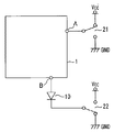
図1は本発明による有機エレクトロルミネッセンス素子を用いたアクティブマトリクス型表示装置の駆動回路を示すブロック図である。同図に示されているように、本例の有機エレクトロルミネッセンス素子駆動回路1は、第1の端子Aを有する。第1の端子Aはスイッチ21により、第1の電位(VCC)を供給する第1の電源線、および、第1の電位よりも低い第2の電位(GND)を供給する第2の電源線のいずれか一方に、電気的に接続可能な構成となっている。
【0031】
また、有機エレクトロルミネッセンス素子駆動回路1は、第2の端子Bを有する。第2の端子Bは有機エレクトロルミネッセンス素子10を介してスイッチ22と電気的に接続されている。第2の端子Bは、スイッチ22により、第1の電位(VCC)を供給する第1の電源線、および、第1の電位よりも低い第2の電位(GND)を供給する第2の電源線のいずれか一方に、有機エレクトロルミネッセンス素子10を介して電気的に接続可能な構成となっている。尚、第1の電位(VCC)は、第2の電位(GND)よりも高い電位であり、例えば10V程度である。
【0032】
有機エレクトロルミネッセンス素子10を発光させる場合(第1の動作状態)、すなわち表示を行う場合には、スイッチ21を第1の電位(VCC)を供給する第1の電源線側に設定し、スイッチ22を第2の電位(GND)を供給する第2の電源線側に設定すれば良い。このとき、第1の端子Aは第1の電源線と電気的に接続され、第2の端子Bは有機エレクトロルミネッセンス素子10を介して第2の電源線と電気的に接続される。
【0033】
一方、有機エレクトロルミネッセンス素子10を発光させない場合(第2の動作状態)、すなわち表示を行わない場合には、スイッチ21を第2の電位(GND)を供給する第2の電源線側に設定し、スイッチ22を第1の電位(VCC)を供給する第1の電源線側に設定すれば良い。このとき、第1の端子Aは第2の電源線と電気的に接続され、第2の端子Bは有機エレクトロルミネッセンス素子10を介して第1の電源線と電気的に接続される。このような電気的接続関係のときには、端子Bの電位が第1の電位(VCC)より大きくなることはないので、有機エレクトロルミネッセンス素子10に逆バイアスが印加されることになる。但し、上記のような電気的接続関係を、有機エレクトロルミネッセンス素子が第2の動作状態である全期間において続ける必要は無い。有機エレクトロルミネッセンス素子が第2の動作状態にある期間のうちの少なくとも一部期間において、上記のような電気的接続関係を保てれば良い。
【0034】
このように、スイッチ21及び22の設定を切換えるだけで、有機エレクトロルミネッセンス素子に逆バイアスを印加することができるのである。そして、この場合、もともと用意されている電源やGNDを利用するため、新たにマイナス電源などの追加電源を用意する必要がないので、消費電力が増加したり、コストの増加を招くことはない。なお、これらのスイッチ21及び22は、トランジスタを組み合わせて簡単に実現できる。
【0035】
【実施例】
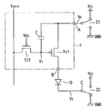
図2は、第1の実施例による駆動回路の内部構成を示すブロック図である。同図においては、前述した図8の回路構成を駆動回路1としている。すなわち、駆動回路1は、有機エレクトロルミネッセンス素子10の動作状態を制御するための駆動トランジスタTr1と、このトランジスタTr1をオン状態に保持するための電荷を蓄積する容量素子2と、外部信号に応じて容量素子2への充電を制御する充電制御トランジスタTr2とを含んで構成されている。そして、駆動回路1においては、容量素子2を構成する一方の電極は第1の端子Aに電気的に接続され、容量素子2を構成する他方の電極は駆動トランジスタTr1のゲート電極に電気的に接続されている。さらに、駆動トランジスタTr1を構成する一方のソースまたはドレインは第1の端子Aに電気的に接続され、駆動トランジスタTr1を構成する他方のソースまたはドレインは第2の端子Bに電気的に接続されている。このため、第1の端子Aと第2の端子Bとが駆動トランジスタTr1のソース及びドレインを介して電気的に接続されていることになる。
【0036】
そして、第1の端子Aと第2の端子Bとの電気的接続状態をスイッチ21及び22によって切換えているのである。すなわち、有機エレクトロルミネッセンス素子10を発光させる場合(第1の動作状態)には、スイッチ21を電源電位VCC側に設定し、スイッチ22をGND側に設定する。この状態において容量素子2を充電し、トランジスタTr1をオン状態にして有機エレクトロルミネッセンス素子10に電流を流せば良い。
【0037】
一方、有機エレクトロルミネッセンス素子10を発光させない場合(第2の動作状態)には、スイッチ21をGND側に設定し、スイッチ22を電源電位VCC側に設定すれば良い。この場合、図3に示されているように、選択電位VSELを電源電位VCCに保っておく。第1の端子Aの電位(VD)を電源電位VCCからGNDに低下させ、この低下後に、第3の端子Cの電位(VS)をGNDから電源電位VCCに上昇させる。すると、駆動トランジスタTr1のゲート電位V1は電位VDの変化に追従して低下する。通常、トランジスタTr1のゲート線には配線容量(図示せず)が付加されるが、その容量の大きさが容量素子2の容量に対して無視できる程度であれば、第1の端子Aの電位VDが電源電位VCCからGNDに変化したときには、トランジスタTr1のゲート電位V1は電源電位VCC分だけ低下する。このとき、第2の端子Bの電位は最大でも駆動トランジスタTr1のしきい値電圧(Vth)であり、第3の端子Cの電位VSは電源電位VCCになるので、有機エレクトロルミネッセンス素子10に逆バイアスが印加されることになる。
【0038】
このように、スイッチ21及び22の設定を切換えるだけで、有機エレクトロルミネッセンス素子に逆バイアスを印加することができる。そして、新たにマイナス電源などの追加電源を用意する必要がないので、消費電力が増加したり、コストが大幅に増大することはない。
【0039】
図4は、第2の実施例による駆動回路の内部構成を示すブロック図である。同図においては、前述した図10の回路構成を駆動回路1としている。すなわち、駆動回路1は、有機エレクトロルミネッセンス素子10の動作状態を制御するための駆動トランジスタTr1と、このトランジスタTr1の導通状態を制御するための電荷を蓄積する容量素子2と、外部信号に応じて容量素子2への充電を制御する充電制御トランジスタTr2とを含んで構成されている。そして、駆動回路1においては、容量素子2を構成する一方の電極は第2の選択トランジスタTr4を介して第1の端子Aに電気的に接続され、容量素子2を構成する他方の電極は駆動トランジスタTr1のゲート電極に電気的に接続されている。さらに、駆動トランジスタTr1の一端は第2の選択トランジスタTr4を介して第1の端子Aに電気的に接続され、駆動トランジスタTr1の他端は第2の端子Bに電気的に接続されている。このため、第1の端子Aと第2の端子Bとが、駆動トランジスタTr1及び選択トランジスタTr4のソース及びドレインを介して電気的に接続されることになる。
【0040】
ここでよく知られているようにトランジスタは同一規格のものでも特性にはばらつきがあり、従って、トランジスタのゲート電極に同一の電圧を印加したとしても必ずしもトランジスタに一定値の電流が流れる訳ではなく、これが輝度むら等の要因となることがある。これに対してこの駆動回路では、電流源4から出力されるデータ信号に応じた電流量に基づいて容量素子2に電荷が蓄積される。従って、データに応じた電流量に基づいて有機エレクトロルミネッセンスの発光状態を制御できる。
【0041】
この駆動回路において、第1の端子Aと第2の端子Bの電気的接続状態は、スイッチ21及び22によって、電源電位VCC及びGNDに切換えられる。すなわち、有機エレクトロルミネッセンス素子10を発光させる場合には、スイッチ21を電源電位VCC側に設定し、スイッチ22をGND側に設定し、さらにトランジスタTr1をオン状態にすると共にトランジスタTr4をオン状態にして、有機エレクトロルミネッセンス素子10に電流を流せば良い。
【0042】
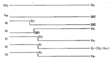
一方、有機エレクトロルミネッセンス素子10に逆バイアスを印加する場合には、スイッチ21をGND側に設定し、スイッチ22を電源電位VCC側に設定すれば良い。この場合、図5に示すように、選択電位VSELを電源電位VCCに、データ保持制御信号VgpをGNDに保っておく。そして、第1の端子Aの電位VDを電源電位VCCからGNDに低下させる。この低下後に、第3の端子Cの電位VSをGNDから電源電位VCCに上昇させる。なお、図5にはこの駆動回路における電流書き込み後の動作のみが示されている。
【0043】
ノードDの電位V1は、トランジスタTr4が常時オン状態であることから、第1の端子Aの電位VDが電源電位VCCからGNDに低下したことに追従して、電源電位VCCからトランジスタTr4のしきい値電圧Vthに低下する。このとき、通常であればトランジスタTr1のゲート線には配線容量(図示せず)が付加されるが、その容量の大きさが容量素子2の容量に対して無視できる程度であれば、ノードEの電位V2は、V2−(VCC−Vth)と変化する。さらに、電位V2≦VCC−Vthの場合、第2の端子Bの電位電位V3はしきい値電圧Vthに低下する。尚、以上の記載はトランジスタTr1とTr4のしきい値電圧が等しいことを前提としている。このようにして、有機エレクトロルミネッセンス素子10に逆バイアスが印加されることになる。
【0044】
このように、スイッチの設定を切換えるだけで、有機エレクトロルミネッセンス素子への逆バイアスの印加が実現できる。そして、新たにマイナス電源などの追加電源を用意する必要がないので、消費電力が増加したり、コストが大幅に増大することはない。
【0045】
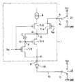
図6は、第3の実施例による駆動回路の内部構成を示すブロック図である。同図においては、特開平11−272233号公報に記載されている回路を駆動回路1としている。すなわち、駆動回路1は、有機エレクトロルミネッセンス素子10の動作状態を制御するための駆動トランジスタTr1と、このトランジスタTr1をオン状態に保持するための電荷を蓄積する容量素子2と、外部信号に応じて容量素子2の電荷の蓄積状態を制御する充電制御トランジスタTr5とを含んで構成されている。そして、駆動回路1においては、容量素子2を構成する一方の電極は駆動トランジスタTr1のゲート電極に電気的に接続され、容量素子2を構成する他方の電極はGNDに電気的に接続されている。さらに、駆動トランジスタTr1を構成する一方のソースまたはドレインは第1の端子Aに電気的に接続され、駆動トランジスタTr1を構成する他方のソースまたはドレインは第2の端子Bに電気的に接続されている。このため、第1の端子Aと第2の端子Bとが駆動トランジスタTr1のソース及びドレインを介して電気的に接続されていることになる。尚、同図におけるトランジスタTr1,Tr6は、Pチャネル型トランジスタ、トランジスタTr5,Tr7はNチャネル型トランジスタである。また、ダイオード接続されたトランジスタTr6は、トランジスタTr1のしきい値のばらつきを補償する効果がある。
【0046】
この駆動回路において、第1の端子Aと第2の端子Bの電気的接続状態は、スイッチ21及び22によって、電源電位VCC及びGNDに切換えられる。すなわち、有機エレクトロルミネッセンス素子10を発光させる場合には、スイッチ21を電源電位VCC側に設定し、スイッチ22をGND側に設定する。この状態においてトランジスタTr5をオン状態にし、トランジスタTr6を介して容量素子2を充電する。この充電レベルに応じてトランジスタTr1のソース−ドレイン間のコンダクタンスを制御し、有機エレクトロルミネッセンス素子10に電流を流せば良い。
【0047】
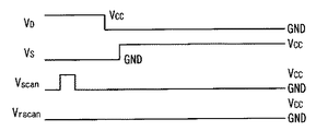
一方、有機エレクトロルミネッセンス素子10に逆バイアスを印加する場合には、スイッチ21をGND側に設定し、スイッチ22を電源電位VCC側に設定すれば良い。この場合、図7に示されているように、最初に充電制御トランジスタTr5のゲート電極に印加する電位Vscanを電源電位VCCにして容量素子2を充電する。このとき、トランジスタTr1をオンさせるのに充分な電荷を容量素子2に保持させる(充電する)期間だけ電源電位VCCにする。データ線VDATAはトランジスタTr1がオンする電位になっていることが必要である。この充電後、スイッチ21を切換えて第1の端子Aの電位VDをVCCからGNDに低下させ、さらにその後スイッチ22を切換えて第3の端子Cの電位VSをGNDからVCCに上昇させる。なお、Tr7はリセット用のトランジスタであり、有機エレクトロルミネッセンス素子10に逆バイアスをかけているときには、このトランジスタTr7をオフ状態にするために電位VrscanをGNDに保持しておく。
【0048】
このように、スイッチの設定を切換えるだけで、有機エレクトロルミネッセンス素子に逆バイアスを印加できる。そして、新たにマイナス電源などの追加電源を用意する必要がないので、消費電力が増加したり、コストが大幅に増大することはない。
【0049】
なお、以上の各実施例においては、タイミングをずらして2つのスイッチ21及び22を切換えているが、これらスイッチを同時に切換えても良いことは明らかである。切換え制御するための制御信号を、タイミングをずらして2つのスイッチに入力すれば、異なるタイミングで2つのスイッチを切換えることができる。この場合、2つのスイッチそれぞれの制御信号を、異なる段数のバッファを介して入力すれば良い。
【0050】
ところで、以上では有機エレクトロルミネッセンス素子を用いたアクティブマトリクス型表示装置の駆動回路について説明したが、本発明の適用範囲はこれに限られず、例えば、TFT−LCD、FED(Field Emission Display)、電気泳動素子や電場反転素子、レーザーダイオード、LEDなど、有機エレクトロルミネッセンス素子以外の電気光学素子を用いたアクティブマトリクス型表示装置にも適用することができる。
【0051】
つぎに、以上に説明した駆動回路1を備えて構成されるアクティブマトリクス型表示装置を適用した電子機器のいくつかの事例について説明する。図14はこのアクティブマトリクス型表示装置を適用したモバイル型のパーソナルコンピュータの構成を示す斜視図である。この図において、パーソナルコンピュータ1100は、キーボード1102を備えた本体部1104と、表示ユニット1106とにより構成され、この表示ユニット1106が前記アクティブマトリクス型表示装置100を備えている。
【0052】
また、図15は前述の駆動回路を備えて構成されるアクティブマトリクス型表示装置100をその表示部に適用した携帯電話機の構成を示す斜視図である。この図において、携帯電話機1200は、複数の操作ボタン1202のほか、受話口1204、送話口1206とともに、前記のアクティブマトリクス型表示装置100を備えている。
【0053】
また、図16は前述の駆動回路を備えて構成されるアクティブマトリクス型表示装置100をそのファインダに適用したディジタルスチルカメラの構成を示す斜視図である。なお、この図には外部機器との接続についても簡易的に示している。ここで通常のカメラは、被写体の光像によりフィルムを感光するのに対し、ディジタルスチルカメラ1300は、被写体の光像をCCD(Charge Coupled Device)などの撮像素子により光電変換して撮像信号を生成する。ディジタルスチルカメラ1300におけるケース1302の背面には、アクティブマトリクス型表示装置100が設けられ、CCDによる撮像信号に基づいて表示を行う構成になっており、アクティブマトリクス型表示装置100は被写体を表示するファインダとして機能する。また、ケース1302の観察側(図においては裏面側)には、光学レンズやCCDなどを含んだ受光ユニット1304が設けられている。
【0054】
撮影者が駆動回路に表示された被写体像を確認しシャッタボタン1306を押下すると、その時点におけるCCDの撮像信号が、回路基板1308のメモリに転送・格納される。また、このディジタルスチルカメラ1300にあっては、ケース1302の側面に、ビデオ信号出力端子1312と、データ通信用の入出力端子1314とが設けられている。そして、図に示されるように、前者のビデオ信号出力端子1312にはテレビモニタ1430が、また、後者のデータ通信用の入出力端子1314にはパーソナルコンピュータ1430が、それぞれ必要に応じて接続される。さらに、所定の操作により回路基板1308のメモリに格納された撮像信号が、テレビモニタ1430や、パーソナルコンピュータ1440に出力される構成になっている。
【0055】
なお、本発明のアクティブマトリクス型表示装置100が適用される電子機器としては、図14のパーソナルコンピュータや、図15の携帯電話、図16のディジタルスチルカメラの他にも、液晶テレビや、ビューファインダ型、モニタ直視型のビデオテープレコーダ、カーナビゲーション装置、ページャ、電子手帳、電卓、ワードプロセッサ、ワークステーション、テレビ電話、POS端末、タッチパネルを備えた機器等などが挙げられる。そして、これらの各種電子機器の表示部として、前述したアクティブマトリクス型表示装置100が適用可能であることは言うまでもない。
【0056】
【発明の効果】
以上説明したように本発明は、第1の電位からなる第1の電源と第2の電位からなる第2の電源との接続状態をスイッチで切換えることにより、新たにマイナス電源などの追加電源を用意する必要がなく、消費電力の増加やコストの増大をほとんど伴わずに逆バイアス印加を実現できるという効果がある。
【図面の簡単な説明】
【図1】本発明による有機エレクトロルミネッセンス素子駆動回路の実施の一形態を示すブロック図である。
【図2】本発明による有機エレクトロルミネッセンス素子駆動回路の第1の実施例を示すブロック図である。
【図3】図2の有機エレクトロルミネッセンス素子駆動回路の動作を示す波形図である。
【図4】本発明による有機エレクトロルミネッセンス素子駆動回路の第2の実施例を示すブロック図である。
【図5】図4の回路の動作を示す波形図である。
【図6】本発明による有機エレクトロルミネッセンス素子駆動回路の第3の実施例を示すブロック図である。
【図7】図6の回路の動作を示す波形図である。
【図8】従来の有機エレクトロルミネッセンス素子駆動回路の構成例を示すブロック図である。
【図9】図8の回路の動作を示す波形図である。
【図10】従来の有機エレクトロルミネッセンス素子駆動回路の他の構成例を示すブロック図である。
【図11】図10の回路の動作を示す波形図である。
【図12】従来の有機エレクトロルミネッセンス素子駆動回路の他の構成例を示すブロック図である。
【図13】図12の回路の動作を示す波形図である。
【図14】本発明の一実施例による駆動回路を備えたアクティブマトリクス型表示装置を、モバイル型のパーソナルコンピュータに適用した場合の一例を示す図である。
【図15】本発明の一実施例による駆動回路を備えたアクティブマトリクス型表示装置を、携帯電話機の表示部に適用した場合の一例を示す図である。
【図16】本発明の一実施例による駆動回路を備えたアクティブマトリクス型表示装置を、ファインダ部分に適用したディジタルスチルカメラの斜視図を示す図である。
【符号の説明】
1 駆動回路
2 容量素子
4 電流源
10 有機エレクトロルミネッセンス素子
21,22 スイッチ
Tr1〜Tr7 トランジスタ[0001]
BACKGROUND OF THE INVENTION
The present invention relates to a drive circuit for an active matrix display device using an electro-optical element such as an organic electroluminescent element (hereinafter referred to as “organic electroluminescent element”), an electronic apparatus, and a driving method for the electro-optical apparatus. The present invention relates to an electro-optical device, and more particularly, to a driving circuit and an electronic apparatus having a function of applying a reverse bias to the electro-optical element to suppress deterioration of the electro-optical element, a driving method of the electro-optical device, and the electro-optical device.
[0002]
[Prior art]
It is known that a display device can be realized by arranging a plurality of pixels composed of an organic electroluminescence element which is one of electro-optical elements in a matrix. The organic electroluminescence device has an organic laminated thin film including a light emitting layer between a cathode made of a metal electrode such as Mg: Ag and AL: Li and an anode made of a transparent electrode made of ITO (Indium Tin Oxide). Take.
[0003]
FIG. 8 shows a general configuration of a drive circuit of an active matrix display device using an organic electroluminescence element. In the figure, the organic electroluminescence element is represented as a
[0004]
Both the transistors Tr1 and Tr2 are assumed to be P-channel TFTs. The transistor Tr1 is on / off controlled in accordance with the charge accumulated in the
[0005]
A simple timing chart for the circuit of FIG. 8 is shown in FIG. As shown in FIG. 9, when data is written, the selection potential V SEL Is set to the low level to turn on the transistor Tr2, thereby charging the
[0006]
FIG. 10 shows another configuration of the drive circuit for the organic electroluminescence element. The drive circuit shown in the figure is described in a document “The Impact of Transient Response of Organic Light Organic Light Emitting Diodes on the Design of Active Matrix OLED Displays” (1998 IEEE IEDM 98-875). 10, Tr1 is a drive transistor, Tr2 is a charge control transistor, Tr3 is a first selection transistor, and Tr4 is a second selection transistor that is turned off during the charging period of the
[0007]
As is well known here, even if the transistors are of the same standard, there are variations in characteristics. Therefore, even if the same voltage is applied to the gate electrode of the transistor, a constant current does not necessarily flow through the transistor. This may cause luminance unevenness. On the other hand, in this drive circuit, charges are accumulated in the
[0008]
The transistors Tr1 to Tr4 are all P-channel MOS transistors and have a selection potential V SEL Is set to a low level to turn on the transistors Tr2 and Tr3, and a charge having a value corresponding to the output of the current source 4 is accumulated in the
[0009]
A simple timing chart for the circuit of FIG. 10 is shown in FIG. As shown in FIG. 11, when data is written by the current source 4, the selection potential V SEL Is set to a low level to turn on the transistors Tr2 and Tr3 and charge the
[0010]
FIG. 12 shows still another configuration of the organic electroluminescence element driving circuit. The drive circuit shown in the figure is a circuit described in Japanese Patent Laid-Open No. 11-272233. In the figure, the drive circuit includes a drive transistor Tr1 that supplies current from the power source to the
[0011]
In this drive circuit, when the
[0012]
[Problems to be solved by the invention]
By the way, it is known that applying a reverse bias to the organic electroluminescence element is an effective means for extending the life of the organic electroluminescence element. This extension of life is described, for example, in JP-A-11-8064.
[0013]
However, in the method disclosed in the publication, when reverse bias is applied to the organic electroluminescence element, it is necessary to prepare an additional power source such as a negative power source and control the organic electroluminescence element to be reverse biased. .
[0014]
Therefore, the present invention provides a drive circuit for an active matrix display device, an electronic apparatus, and an electro-optical device that can apply a reverse bias to an electro-optical device such as an organic electroluminescence device with little increase in power consumption or cost. It is an object to provide a driving method and an electro-optical device.
[0015]
[Means for Solving the Problems]
In order to achieve the above object, a drive circuit for an active matrix display device according to the present invention is a drive circuit for an active matrix display device in which a plurality of pixels are arranged in a matrix, each of the plurality of pixels being A first power line for supplying a first potential and a first potential lower than the first potential, the electro-optic element, a transistor for controlling an operating state of the electro-optic element, and a capacitor element. A first terminal that is electrically connected to any one of a second power supply line that supplies a second potential and the potential is switched between the first potential and the second potential; And a second terminal electrically connected to either one of the first power supply line and the second power supply line via the electro-optic element, and the first electrode of the capacitor element is a source or drain of the transistor and Said And the second electrode of the capacitor is electrically connected to the gate electrode of the transistor, and the first terminal and the second terminal are the source and drain of the transistor. It is characterized by being electrically connected via.
The drive circuit of the active matrix display device of the present invention is the drive circuit of the active matrix display device described above, and when the electro-optical element is in the first operation state, the first terminal is When the second terminal is electrically connected to the first power line and the second terminal is electrically connected to the second power line, and the electro-optical element is in the second operation state, The first terminal is electrically connected to the second power supply line, and the second terminal has at least a timing of being electrically connected to the first power supply line; Features.
A drive circuit for an active matrix display device according to the present invention is the drive circuit for the active matrix display device described above, wherein the transistor provided between the first terminal and the first electrode is It further has a different second transistor.
A drive circuit for an active matrix display device according to the present invention is the drive circuit for the active matrix display device described above, wherein the electro-optic element is an organic electroluminescence element.
In order to achieve the above object, a driving method of an active matrix display device of the present invention is a driving method of an active matrix display device in which a plurality of pixels are arranged in a matrix, each of the plurality of pixels being And an electro-optic element; a transistor for controlling an operating state of the electro-optic element; and a capacitor element for accumulating electric charge for holding the transistor in an on state, and supplying a first potential. One power supply line and a second power supply line that supplies a second potential lower than the first potential, and the potential is connected to the first potential and the second potential. A first terminal that can be switched to any one of the above, and a second terminal that is electrically connected to one of the first and second power lines via the electro-optic element, and 1st terminal When the second terminal is electrically connected via the source and drain of the transistor and the electro-optic element is in the first operating state, the first terminal is the first power line. And the second terminal is in a state of being electrically connected to the second power supply line, and the electro-optical element is in the second operating state, the first terminal Is electrically connected to the second power supply line, and the second terminal is electrically connected to the first power supply line. After the transistor is turned on, the first terminal The operation state is shifted to the second operation state.
The driving method of the active matrix display device of the present invention is the driving method of the above active matrix display device, wherein the first electrode of the capacitor is connected to the source or drain of the transistor and the first terminal. The second electrode of the capacitor is electrically connected to the gate electrode of the transistor, and the transistor is turned on by switching the potential of the first terminal. The first operating state is shifted to the second operating state.
In order to achieve the above object, an electro-optical device of the present invention is an electro-optical device in which a plurality of unit circuits are arranged in a matrix, each of the plurality of unit circuits including an electro-optical element and the electro-optical element. A first power supply line for supplying a first potential and a second potential for supplying a second potential lower than the first potential, the transistor including a transistor for controlling an operation state of the optical element and a capacitor. A first terminal that is electrically connected to any one of the power supply lines and whose potential is switched to either the first potential or the second potential; and the first and second power supply lines A first terminal of the capacitor is electrically connected to the source or drain of the transistor and the first terminal. Connected to the second electric power of the capacitive element. It is electrically connected to a gate electrode of the transistor, wherein the first terminal and the second terminal are electrically connected via the source and drain of said transistor.
In order to achieve the above object, a driving method for an electro-optical device according to the present invention is a driving method for an electro-optical device in which a plurality of unit circuits are arranged in a matrix. An optical element; a transistor for controlling an operation state of the electro-optical element; and a capacitor element for storing electric charge for holding the transistor in an on state. The power supply line and a second power supply line that supplies a second potential lower than the first potential are electrically connected, and the potential is either the first potential or the second potential. And a first terminal electrically connected to one of the first and second power supply lines via the electro-optic element, and the first terminal The terminal and the second terminal When the electro-optic element is in the first operating state, the first terminal is electrically connected to the first power supply line; and The second terminal is electrically connected to the second power supply line, and the first terminal is connected to the second power supply line when the electro-optical element is in the second operation state. When the second terminal is electrically connected to the first power supply line and is shifted from the first operation state to the second operation state, the second terminal is electrically connected. After the transistor is turned on, the second operation state is set.
The electro-optical device driving method of the present invention is the above-described electro-optical device driving method, wherein the first electrode of the capacitor is electrically connected to the source or drain of the transistor and the first terminal. The second electrode of the capacitor is electrically connected to the gate electrode of the transistor, and after the transistor is turned on by switching the potential of the first terminal, the first operation state To the second operation state.
According to another aspect of the invention, there is provided a driving method for an electro-optical device, wherein the electro-optical element is a current driving element driven by a current.
The drive circuit of the first active matrix display device according to the present invention includes:
A drive circuit for actively driving a display device in which a plurality of pixels made of electro-optic elements are arranged in a matrix,
A first terminal electrically connected to one of a first power supply line for supplying a first potential and a second power supply line for supplying a second potential lower than the first potential;
A second terminal electrically connected to either one of the first and second power lines via the electro-optic element,
When the electro-optical element is in the first operating state, the first terminal is electrically connected to the first power supply line, and the second terminal is connected to the first power line via the electro-optical element. 2 is electrically connected to the power line
When the electro-optical element is in the second operating state, the first terminal is electrically connected to the second power supply line, and the second terminal is connected to the second power line via the electro-optical element. It is characterized in that there is at least a timing when it is electrically connected to one power line.
[0016]
The driving circuit of the second active matrix display device according to the present invention includes:
A drive transistor for controlling the operating state of the electro-optic element;
A capacitive element for accumulating charges for holding the driving transistor in an on state; a charge control transistor for controlling charging of the capacitive element in response to an external signal;
Further including
One electrode constituting the capacitive element is electrically connected to the first terminal,
The other electrode constituting the capacitive element is electrically connected to the gate electrode of the driving transistor,
The first terminal and the second terminal are electrically connected through a source and a drain of the driving transistor.
Furthermore, the direction of the current flowing between the source and drain of the driving transistor is different between the first operating state and the second operating state.
[0017]
The driving circuit of the third active matrix type display device according to the present invention comprises:
A drive transistor for controlling the operating state of the electro-optic element;
A capacitive element for accumulating charges for holding the driving transistor in an on state;
A charge control transistor that controls charging of the capacitive element according to an external signal;
Further including
One electrode constituting the capacitor is electrically connected to the first terminal via a selection transistor that is turned off during a charge period of the capacitor,
The other electrode constituting the capacitive element is electrically connected to the gate electrode of the driving transistor,
The first terminal and the second terminal are electrically connected via a source and a drain of the driving transistor and a source and a drain of the selection transistor.
[0018]
The drive circuit of the fourth active matrix display device according to the present invention is:
A drive transistor for controlling the operating state of the electro-optic element;
A capacitive element for accumulating charges for holding the driving transistor in an on state; a charge control transistor for controlling charging of the capacitive element in response to an external signal;
Further including
One electrode constituting the capacitive element is electrically connected to the gate electrode of the driving transistor,
The other electrode constituting the capacitive element is electrically connected to the ground,
The first terminal and the second terminal are electrically connected through a source and a drain of the driving transistor.
[0019]
In short, since the connection state of the first power supply and the second power supply to the drive circuit is switched by a switch, it is not necessary to add a power supply, and the organic electroluminescence element is reverse-biased with little increase in power consumption or cost. Can be applied. In this case, generally, the first power supply is V CC Therefore, the second power source is the ground (GND), and the originally prepared potential is used. However, the present invention is not limited to these as long as a potential difference sufficient to cause the organic electroluminescence element to emit light can be secured.
[0020]
The drive circuit of the fifth active matrix display device of the present invention is characterized in that the electro-optic element is an organic electroluminescence element.
[0021]
A first electronic device according to the present invention is an electronic device on which an active matrix display device including the driving circuit is mounted.
[0022]
The first electro-optical device driving method according to the present invention includes a first power supply line having a first potential, and a second power supply line having a second potential lower than the first potential. An electro-optical device comprising: an electro-optical element electrically disposed between the first power line and the second power line,
When electrically connecting the one end of the electro-optic element to the first power line, the other end of the electro-optic element is connected to the second power line,
When electrically connecting the one end of the electro-optic element to the second power supply line, electrically connecting the other end of the electro-optic element to the first power supply line;
It is characterized by.
[0023]
Note that “electrically arranged” does not necessarily mean that an electro-optical element is directly connected to the power line, but other elements such as transistors are arranged between the power line and the electro-optical element. This is also included. The electro-optical element is, for example, a liquid crystal element, an electrophoretic element, an electroluminescence element, or the like, and means an element that is driven by applying a voltage or supplying a current.
[0024]
According to a second electro-optical device driving method of the present invention, in the electro-optical device driving method, the electro-optical element is a current driving element driven by a current.
It is characterized by.
[0025]
That is, when the electro-optical element is a current driving element, a current in the reverse direction to the forward direction flows through the electro-optical element by this driving method.
[0026]
The first electro-optical device of the present invention includes a first power supply line having a first potential, a second power supply line having a second potential lower than the first potential, and the first power line. An electro-optical device comprising: an electro-optical element electrically disposed between one power line and the second power line,
When one end of the electro-optical element is electrically connected to the first power line, the other end of the electro-optical element is connected to the second power line,
When the one end of the electro-optic element is electrically connected to the second power supply line, the other end of the electro-optic element is electrically connected to the first power supply line;
It is characterized by.
[0027]
According to a second electro-optical device of the present invention, in the electro-optical device, the electro-optical element is disposed corresponding to an intersection of a data line that supplies a data signal and a scanning line that supplies a scanning signal. Placed in a unit circuit,
It is characterized by.
[0028]
The third electro-optical device of the present invention is the electro-optical device described above.
The unit circuit includes: a first transistor that controls a conduction state of the electro-optic element; a second transistor having a gate electrode connected to the scanning line;
A capacitive element connected to the gate electrode of the first transistor and storing a charge corresponding to the data signal supplied by the data line;
Including,
It is characterized by.
[0029]
DETAILED DESCRIPTION OF THE INVENTION
Next, embodiments of the present invention will be described with reference to the drawings. In the drawings referred to in the following description, the same parts as those in the other drawings are denoted by the same reference numerals.
[0030]
FIG. 1 is a block diagram showing a driving circuit of an active matrix display device using an organic electroluminescence element according to the present invention. As shown in the figure, the organic electroluminescence
[0031]
Further, the organic electroluminescence
[0032]
When the
[0033]
On the other hand, when the
[0034]
As described above, the reverse bias can be applied to the organic electroluminescence element only by switching the setting of the
[0035]
【Example】
FIG. 2 is a block diagram showing the internal configuration of the drive circuit according to the first embodiment. In the figure, the circuit configuration of FIG. That is, the
[0036]
The electrical connection state between the first terminal A and the second terminal B is switched by the
[0037]
On the other hand, when the
[0038]
As described above, the reverse bias can be applied to the organic electroluminescence element only by switching the setting of the
[0039]
FIG. 4 is a block diagram showing the internal configuration of the drive circuit according to the second embodiment. In the figure, the circuit configuration of FIG. That is, the
[0040]
As is well known here, even if the transistors are of the same standard, there are variations in characteristics. Therefore, even if the same voltage is applied to the gate electrode of the transistor, a constant current does not necessarily flow through the transistor. This may cause luminance unevenness. On the other hand, in this drive circuit, charges are accumulated in the
[0041]
In this drive circuit, the electrical connection state between the first terminal A and the second terminal B is determined by the
[0042]
On the other hand, when a reverse bias is applied to the
[0043]
Node V potential V 1 Since the transistor Tr4 is always on, the potential V of the first terminal A D Is the power supply potential V CC Following the drop from GND to GND, the power supply potential V CC To threshold voltage V of transistor Tr4 th To drop. At this time, a wiring capacitance (not shown) is usually added to the gate line of the transistor Tr1, but if the capacitance is negligible with respect to the capacitance of the
[0044]
In this way, application of a reverse bias to the organic electroluminescence element can be realized only by changing the setting of the switch. In addition, since it is not necessary to prepare an additional power source such as a negative power source, the power consumption does not increase and the cost does not increase significantly.
[0045]
FIG. 6 is a block diagram showing the internal configuration of the drive circuit according to the third embodiment. In the figure, the circuit described in Japanese Patent Application Laid-Open No. 11-272233 is used as the
[0046]
In this drive circuit, the electrical connection state between the first terminal A and the second terminal B is determined by the
[0047]
On the other hand, when a reverse bias is applied to the
[0048]
As described above, the reverse bias can be applied to the organic electroluminescence element only by changing the setting of the switch. In addition, since it is not necessary to prepare an additional power source such as a negative power source, the power consumption does not increase and the cost does not increase significantly.
[0049]
In the above embodiments, the two
[0050]
By the way, the drive circuit of the active matrix display device using the organic electroluminescence element has been described above. However, the scope of application of the present invention is not limited to this. For example, TFT-LCD, FED (Field Emission Display), electrophoresis The present invention can also be applied to an active matrix display device using an electro-optical element other than an organic electroluminescence element such as an element, an electric field inverting element, a laser diode, or an LED.
[0051]
Next, some examples of electronic devices to which the active matrix display device configured by including the
[0052]
FIG. 15 is a perspective view showing a configuration of a mobile phone in which the active
[0053]
FIG. 16 is a perspective view showing a configuration of a digital still camera in which the active
[0054]
When the photographer confirms the subject image displayed on the drive circuit and presses the
[0055]
Note that electronic devices to which the active
[0056]
【The invention's effect】
As described above, according to the present invention, an additional power source such as a negative power source can be newly added by switching the connection state between the first power source having the first potential and the second power source having the second potential. There is no need to prepare, and there is an effect that reverse bias application can be realized with little increase in power consumption and cost.
[Brief description of the drawings]
FIG. 1 is a block diagram showing an embodiment of an organic electroluminescence element driving circuit according to the present invention.
FIG. 2 is a block diagram showing a first embodiment of an organic electroluminescence element driving circuit according to the present invention.
3 is a waveform diagram showing an operation of the organic electroluminescence element driving circuit of FIG. 2. FIG.
FIG. 4 is a block diagram showing a second embodiment of the organic electroluminescence element driving circuit according to the present invention.
FIG. 5 is a waveform diagram showing an operation of the circuit of FIG. 4;
FIG. 6 is a block diagram showing a third embodiment of the organic electroluminescence element driving circuit according to the present invention.
7 is a waveform diagram showing an operation of the circuit of FIG. 6. FIG.
FIG. 8 is a block diagram illustrating a configuration example of a conventional organic electroluminescence element driving circuit.
9 is a waveform chart showing the operation of the circuit of FIG.
FIG. 10 is a block diagram showing another configuration example of a conventional organic electroluminescence element driving circuit.
11 is a waveform diagram showing an operation of the circuit of FIG.
FIG. 12 is a block diagram showing another configuration example of a conventional organic electroluminescence element driving circuit.
13 is a waveform chart showing the operation of the circuit of FIG.
FIG. 14 is a diagram showing an example when an active matrix display device including a drive circuit according to an embodiment of the present invention is applied to a mobile personal computer.
FIG. 15 is a diagram showing an example in which an active matrix display device including a driving circuit according to an embodiment of the present invention is applied to a display unit of a mobile phone.
FIG. 16 is a diagram showing a perspective view of a digital still camera in which an active matrix display device having a drive circuit according to an embodiment of the present invention is applied to a finder portion.
[Explanation of symbols]
1 Drive circuit
2 Capacitance element
4 Current source
10 Organic electroluminescence device
21 and 22 switches
Tr1-Tr7 transistors
Claims (11)
複数の画素の各々は、電気光学素子と、前記電気光学素子の動作状態を制御するためのトランジスタと、容量素子と、を備え、
第1の電位を供給する第1の電源線及び前記第1の電位よりも低い第2の電位を供給する第2の電源線のいずれか一方に電気的に接続され、その電位が前記第1の電位及び前記第2の電位のいずれかに切り替えられる第1の端子と、
前記第1及び前記第2の電源線のいずれか一方に前記電気光学素子を介して電気的に接続される第2の端子と、を含み、
前記容量素子の第1電極は前記トランジスタのソース又はドレイン及び前記第1の端子に電気的に接続され、前記容量素子の第2電極は前記トランジスタのゲート電極に電気的に接続されており、
前記第1の端子と前記第2の端子とが前記トランジスタのソース及びドレインを介して電気的に接続されていることを特徴とするアクティブマトリクス型表示装置の駆動回路。A drive circuit for an active matrix display device in which a plurality of pixels are arranged in a matrix,
Each of the plurality of pixels includes an electro-optical element, a transistor for controlling an operation state of the electro-optical element, and a capacitor element.
The first power supply line supplying a first potential and the second power supply line supplying a second potential lower than the first potential are electrically connected, and the potential is the first power supply line. A first terminal that is switched to one of the potential and the second potential;
A second terminal electrically connected to either one of the first and second power lines via the electro-optic element,
A first electrode of the capacitor is electrically connected to a source or drain of the transistor and the first terminal; a second electrode of the capacitor is electrically connected to a gate electrode of the transistor;
The drive circuit for an active matrix display device, wherein the first terminal and the second terminal are electrically connected through a source and a drain of the transistor.
前記電気光学素子が第1の動作状態であるときには、前記第1の端子は前記第1の電源線に電気的に接続され、かつ、前記第2の端子は前記第2の電源線に電気的に接続された状態となり、
前記電気光学素子が第2の動作状態であるときには、前記第1の端子は前記第2の電源線に電気的に接続され、かつ、前記第2の端子は前記第1の電源線に電気的に接続された状態となるタイミングが少なくともあること、を特徴とするアクティブマトリクス型表示装置の駆動回路。A drive circuit for an active matrix display device according to claim 1,
When the electro-optical element is in the first operating state, the first terminal is electrically connected to the first power supply line, and the second terminal is electrically connected to the second power supply line. Connected to the
When the electro-optical element is in the second operating state, the first terminal is electrically connected to the second power supply line, and the second terminal is electrically connected to the first power supply line. A drive circuit for an active matrix display device, characterized in that there is at least a timing of being connected to the active matrix display device.
前記第1の端子と前記第1電極との間に設けられた前記トランジスタとは異なる第2のトランジスタを更に有することを特徴とするアクティブマトリクス型表示装置の駆動回路。A drive circuit for an active matrix display device according to claim 1 or 2,
The drive circuit for an active matrix display device, further comprising a second transistor different from the transistor provided between the first terminal and the first electrode.
複数の画素の各々は、電気光学素子と、前記電気光学素子の動作状態を制御するためのトランジスタと、前記トランジスタをオン状態に保持するための電荷を蓄積する容量素子と、を備え、
第1の電位を供給する第1の電源線及び前記第1の電位よりも低い第2の電位を供給する第2の電源線のいずれか一方に電気的に接続され、その電位が前記第1の電位及び前記第2の電位のいずれかに切り替えられる第1の端子と、
前記第1及び前記第2の電源線のいずれか一方に前記電気光学素子を介して電気的に接続される第2の端子と、を含み、
前記第1の端子と前記第2の端子とが前記トランジスタのソース及びドレインを介して電気的に接続されており、
前記電気光学素子が第1の動作状態であるときには、前記第1の端子は前記第1の電源線に電気的に接続され、かつ、前記第2の端子は前記第2の電源線に電気的に接続された状態となり、
前記電気光学素子が第2の動作状態であるときには、前記第1の端子は前記第2の電源線に電気的に接続され、かつ、前記第2の端子は前記第1の電源線に電気的に接続された状態となり、
前記トランジスタをオン状態とした後に、前記第1の動作状態から前記第2の動作状態に移行させることを特徴とするアクティブマトリクス型表示装置の駆動方法。A driving method of an active matrix display device in which a plurality of pixels are arranged in a matrix,
Each of the plurality of pixels includes an electro-optic element, a transistor for controlling an operation state of the electro-optic element, and a capacitor element that accumulates electric charge for holding the transistor in an on state,
The first power supply line supplying a first potential and the second power supply line supplying a second potential lower than the first potential are electrically connected, and the potential is the first power supply line. A first terminal that is switched to one of the potential and the second potential;
A second terminal electrically connected to either one of the first and second power lines via the electro-optic element,
The first terminal and the second terminal are electrically connected via the source and drain of the transistor;
When the electro-optical element is in the first operating state, the first terminal is electrically connected to the first power supply line, and the second terminal is electrically connected to the second power supply line. Connected to the
When the electro-optical element is in the second operating state, the first terminal is electrically connected to the second power supply line, and the second terminal is electrically connected to the first power supply line. Connected to the
A driving method of an active matrix display device, wherein after the transistor is turned on, the first operating state is shifted to the second operating state.
前記容量素子の第1電極は前記トランジスタのソース又はドレイン及び前記第1の端子に電気的に接続され、前記容量素子の第2電極は前記トランジスタのゲート電極に電気的に接続されており、
前記第1の端子の電位を切り替えることにより前記トランジスタをオン状態とした後に、前記第1の動作状態から前記第2の動作状態に移行させることを特徴とするアクティブマトリクス型表示装置の駆動方法。A driving method of an active matrix display device according to claim 6,
A first electrode of the capacitor is electrically connected to a source or drain of the transistor and the first terminal; a second electrode of the capacitor is electrically connected to a gate electrode of the transistor;
A driving method of an active matrix display device, wherein after the transistor is turned on by switching the potential of the first terminal, the transistor is shifted from the first operation state to the second operation state.
複数の単位回路の各々は、電気光学素子と、前記電気光学素子の動作状態を制御するためのトランジスタと、容量素子と、を備え、
第1の電位を供給する第1の電源線及び前記第1の電位よりも低い第2の電位を供給する第2の電源線のいずれか一方に電気的に接続され、その電位が前記第1の電位及び前記第2の電位のいずれかに切り替えられる第1の端子と、
前記第1及び前記第2の電源線のいずれか一方に前記電気光学素子を介して電気的に接続される第2の端子と、を含み、
前記容量素子の第1電極は前記トランジスタのソース又はドレイン及び前記第1の端子に電気的に接続され、前記容量素子の第2電極は前記トランジスタのゲート電極に電気的に接続されており、
前記第1の端子と前記第2の端子とが前記トランジスタのソース及びドレインを介して電気的に接続されていることを特徴とする電気光学装置。An electro-optical device in which a plurality of unit circuits are arranged in a matrix,
Each of the plurality of unit circuits includes an electro-optic element, a transistor for controlling an operation state of the electro-optic element, and a capacitive element,
The first power supply line supplying a first potential and the second power supply line supplying a second potential lower than the first potential are electrically connected, and the potential is the first power supply line. A first terminal that is switched to one of the potential and the second potential;
A second terminal electrically connected to either one of the first and second power lines via the electro-optic element,
A first electrode of the capacitor is electrically connected to a source or drain of the transistor and the first terminal; a second electrode of the capacitor is electrically connected to a gate electrode of the transistor;
The electro-optical device, wherein the first terminal and the second terminal are electrically connected through a source and a drain of the transistor.
複数の単位回路の各々は、電気光学素子と、前記電気光学素子の動作状態を制御するためのトランジスタと、前記トランジスタをオン状態に保持するための電荷を蓄積する容量素子と、を備え、
第1の電位を供給する第1の電源線及び前記第1の電位よりも低い第2の電位を供給する第2の電源線のいずれか一方に電気的に接続され、その電位が前記第1の電位及び前記第2の電位のいずれかに切り替えられる第1の端子と、
前記第1及び前記第2の電源線のいずれか一方に前記電気光学素子を介して電気的に接続される第2の端子と、を含み、
前記第1の端子と前記第2の端子とが前記トランジスタのソース及びドレインを介して電気的に接続されており、
前記電気光学素子が第1の動作状態であるときには、前記第1の端子は前記第1の電源線に電気的に接続され、かつ、前記第2の端子は前記第2の電源線に電気的に接続された状態となり、
前記電気光学素子が第2の動作状態であるときには、前記第1の端子は前記第2の電源線に電気的に接続され、かつ、前記第2の端子は前記第1の電源線に電気的に接続された状態となり、
前記第1の動作状態から前記第2の動作状態に移行する際に、前記トランジスタをオン状態とした後に、前記第2の動作状態とすることを特徴とする電気光学装置の駆動方法。A method for driving an electro-optical device in which a plurality of unit circuits are arranged in a matrix,
Each of the plurality of unit circuits includes an electro-optic element, a transistor for controlling an operation state of the electro-optic element, and a capacitor element that accumulates electric charge for holding the transistor in an on state,
The first power supply line supplying a first potential and the second power supply line supplying a second potential lower than the first potential are electrically connected, and the potential is the first power supply line. A first terminal that is switched to one of the potential and the second potential;
A second terminal electrically connected to either one of the first and second power lines via the electro-optic element,
The first terminal and the second terminal are electrically connected via the source and drain of the transistor;
When the electro-optical element is in the first operating state, the first terminal is electrically connected to the first power supply line, and the second terminal is electrically connected to the second power supply line. Connected to the
When the electro-optical element is in the second operating state, the first terminal is electrically connected to the second power supply line, and the second terminal is electrically connected to the first power supply line. Connected to the
A method for driving an electro-optical device, wherein the second operation state is set after the transistor is turned on when shifting from the first operation state to the second operation state.
前記容量素子の第1電極は前記トランジスタのソース又はドレイン及び前記第1の端子に電気的に接続され、前記容量素子の第2電極は前記トランジスタのゲート電極に電気的に接続されており、
前記第1の端子の電位を切り替えることにより前記トランジスタをオン状態とした後に、前記第1の動作状態から前記第2の動作状態に移行させることを特徴とする電気光学装置の駆動方法。A method for driving an electro-optical device according to claim 9,
A first electrode of the capacitor is electrically connected to a source or drain of the transistor and the first terminal; a second electrode of the capacitor is electrically connected to a gate electrode of the transistor;
A method for driving an electro-optical device, wherein the transistor is turned on by switching the potential of the first terminal and then shifted from the first operation state to the second operation state.
前記電気光学素子は電流により駆動される電流駆動素子であることを特徴とする電気光学装置の駆動方法。The driving method of the electro-optical device according to claim 9 or 10,
The method of driving an electro-optical device, wherein the electro-optical element is a current driving element driven by a current.
Priority Applications (9)
| Application Number | Priority Date | Filing Date | Title |
|---|---|---|---|
| JP2001254850A JP3736399B2 (en) | 2000-09-20 | 2001-08-24 | Drive circuit for active matrix display device, electronic apparatus, drive method for electro-optical device, and electro-optical device |
| TW090122508A TW508553B (en) | 2000-09-20 | 2001-09-11 | Driving circuit for active matrix type display, drive method of electronic equipment and electronic apparatus, and electronic apparatus |
| KR1020010055687A KR20020022572A (en) | 2000-09-20 | 2001-09-11 | Circuit of driving active matrix type display device, electronic equipment, method of driving electronic device and electronic device |
| CNB011331585A CN1172281C (en) | 2000-09-20 | 2001-09-19 | Drive electronic device and drive method for active matrix display |
| EP10163676.9A EP2228783B1 (en) | 2000-09-20 | 2001-09-20 | Driving circuit for active matrix type display, drive method of electronic equipment and electronic apparatus |
| EP10181739.3A EP2306444B1 (en) | 2000-09-20 | 2001-09-20 | Driving circuit for active matrix type display, drive method of electronic equipment and electronic apparatus |
| EP01308013A EP1191512A3 (en) | 2000-09-20 | 2001-09-20 | Driving circuit for active matrix type display, drive method of electronic equipment and electronic apparatus, and electronic apparatus |
| US09/956,030 US6750833B2 (en) | 2000-09-20 | 2001-09-20 | System and methods for providing a driving circuit for active matrix type displays |
| US10/840,261 US7091939B2 (en) | 2000-09-20 | 2004-05-07 | System and methods for providing a driving circuit for active matrix type displays |
Applications Claiming Priority (3)
| Application Number | Priority Date | Filing Date | Title |
|---|---|---|---|
| JP2000-285329 | 2000-09-20 | ||
| JP2000285329 | 2000-09-20 | ||
| JP2001254850A JP3736399B2 (en) | 2000-09-20 | 2001-08-24 | Drive circuit for active matrix display device, electronic apparatus, drive method for electro-optical device, and electro-optical device |
Publications (3)
| Publication Number | Publication Date |
|---|---|
| JP2002169510A JP2002169510A (en) | 2002-06-14 |
| JP2002169510A5 JP2002169510A5 (en) | 2005-02-24 |
| JP3736399B2 true JP3736399B2 (en) | 2006-01-18 |
Family
ID=26600331
Family Applications (1)
| Application Number | Title | Priority Date | Filing Date |
|---|---|---|---|
| JP2001254850A Expired - Lifetime JP3736399B2 (en) | 2000-09-20 | 2001-08-24 | Drive circuit for active matrix display device, electronic apparatus, drive method for electro-optical device, and electro-optical device |
Country Status (6)
| Country | Link |
|---|---|
| US (2) | US6750833B2 (en) |
| EP (3) | EP2228783B1 (en) |
| JP (1) | JP3736399B2 (en) |
| KR (1) | KR20020022572A (en) |
| CN (1) | CN1172281C (en) |
| TW (1) | TW508553B (en) |
Families Citing this family (157)
| Publication number | Priority date | Publication date | Assignee | Title |
|---|---|---|---|---|
| TW535454B (en) | 1999-10-21 | 2003-06-01 | Semiconductor Energy Lab | Electro-optical device |
| JP3594126B2 (en) * | 2000-10-13 | 2004-11-24 | 日本電気株式会社 | Current drive circuit |
| SG114502A1 (en) | 2000-10-24 | 2005-09-28 | Semiconductor Energy Lab | Light emitting device and method of driving the same |
| JP3757797B2 (en) * | 2001-01-09 | 2006-03-22 | 株式会社日立製作所 | Organic LED display and driving method thereof |
| JP2002215095A (en) * | 2001-01-22 | 2002-07-31 | Pioneer Electronic Corp | Pixel driving circuit of light emitting display |
| JP4869497B2 (en) * | 2001-05-30 | 2012-02-08 | 株式会社半導体エネルギー研究所 | Display device |
| JP4878096B2 (en) * | 2001-09-04 | 2012-02-15 | キヤノン株式会社 | Light emitting element drive circuit |
| EP3716257B1 (en) | 2001-09-07 | 2021-01-20 | Joled Inc. | El display panel, method of driving the same, and el display device |
| US11302253B2 (en) | 2001-09-07 | 2022-04-12 | Joled Inc. | El display apparatus |
| US6858989B2 (en) * | 2001-09-20 | 2005-02-22 | Emagin Corporation | Method and system for stabilizing thin film transistors in AMOLED displays |
| JP3810725B2 (en) | 2001-09-21 | 2006-08-16 | 株式会社半導体エネルギー研究所 | LIGHT EMITTING DEVICE AND ELECTRONIC DEVICE |
| JP4380954B2 (en) * | 2001-09-28 | 2009-12-09 | 三洋電機株式会社 | Active matrix display device |
| TW574529B (en) * | 2001-09-28 | 2004-02-01 | Tokyo Shibaura Electric Co | Organic electro-luminescence display device |
| US10211268B1 (en) | 2012-09-28 | 2019-02-19 | Imaging Systems Technology, Inc. | Large area OLED display |
| JP3859483B2 (en) * | 2001-10-26 | 2006-12-20 | 沖電気工業株式会社 | Driving circuit |
| US7456810B2 (en) | 2001-10-26 | 2008-11-25 | Semiconductor Energy Laboratory Co., Ltd. | Light-emitting device and driving method thereof |
| US7180479B2 (en) * | 2001-10-30 | 2007-02-20 | Semiconductor Energy Laboratory Co., Ltd. | Signal line drive circuit and light emitting device and driving method therefor |
| JP4498669B2 (en) | 2001-10-30 | 2010-07-07 | 株式会社半導体エネルギー研究所 | Semiconductor device, display device, and electronic device including the same |
| US8558783B2 (en) * | 2001-11-20 | 2013-10-15 | E Ink Corporation | Electro-optic displays with reduced remnant voltage |
| JP2003195810A (en) * | 2001-12-28 | 2003-07-09 | Casio Comput Co Ltd | Driving circuit, driving device and driving method for optical method |
| EP1331627B1 (en) | 2002-01-24 | 2012-04-18 | Semiconductor Energy Laboratory Co., Ltd. | Semiconductor device and method of driving the semiconductor device |
| JP4024557B2 (en) * | 2002-02-28 | 2007-12-19 | 株式会社半導体エネルギー研究所 | Light emitting device, electronic equipment |
| CN1662946A (en) * | 2002-04-26 | 2005-08-31 | 东芝松下显示技术有限公司 | Drive method of EL display apparatus |
| GB2388236A (en) * | 2002-05-01 | 2003-11-05 | Cambridge Display Tech Ltd | Display and driver circuits |
| JP3972359B2 (en) | 2002-06-07 | 2007-09-05 | カシオ計算機株式会社 | Display device |
| JP4610843B2 (en) * | 2002-06-20 | 2011-01-12 | カシオ計算機株式会社 | Display device and driving method of display device |
| JP4019843B2 (en) * | 2002-07-31 | 2007-12-12 | セイコーエプソン株式会社 | Electronic circuit, electronic circuit driving method, electro-optical device, electro-optical device driving method, and electronic apparatus |
| JP4123084B2 (en) | 2002-07-31 | 2008-07-23 | セイコーエプソン株式会社 | Electronic circuit, electro-optical device, and electronic apparatus |
| US7119765B2 (en) | 2002-08-23 | 2006-10-10 | Samsung Sdi Co., Ltd. | Circuit for driving matrix display panel with photoluminescence quenching devices, and matrix display apparatus incorporating the circuit |
| JP4103500B2 (en) * | 2002-08-26 | 2008-06-18 | カシオ計算機株式会社 | Display device and display panel driving method |
| JP2004145278A (en) * | 2002-08-30 | 2004-05-20 | Seiko Epson Corp | Electronic circuit, method for driving electronic circuit, electrooptical device, method for driving electrooptical device, and electronic apparatus |
| JP4144462B2 (en) | 2002-08-30 | 2008-09-03 | セイコーエプソン株式会社 | Electro-optical device and electronic apparatus |
| KR100906964B1 (en) * | 2002-09-25 | 2009-07-08 | 삼성전자주식회사 | Element for driving organic light emitting device and display panel for organic light emitting device with the same |
| JP2004117921A (en) * | 2002-09-26 | 2004-04-15 | Toshiba Matsushita Display Technology Co Ltd | Electroluminescence display device and method for driving electroluminescence display device |
| JP2004145300A (en) * | 2002-10-03 | 2004-05-20 | Seiko Epson Corp | Electronic circuit, method for driving electronic circuit, electronic device, electrooptical device, method for driving electrooptical device, and electronic apparatus |
| CN100472596C (en) | 2002-10-09 | 2009-03-25 | 三菱电机株式会社 | Constant current circuit,drive circuit and image display device |
| JP2004138773A (en) * | 2002-10-17 | 2004-05-13 | Tohoku Pioneer Corp | Active type light emission display device |
| US7423617B2 (en) * | 2002-11-06 | 2008-09-09 | Tpo Displays Corp. | Light emissive element having pixel sensing circuit |
| JP2004157467A (en) | 2002-11-08 | 2004-06-03 | Tohoku Pioneer Corp | Driving method and driving-gear of active type light emitting display panel |
| CN1319035C (en) * | 2003-02-17 | 2007-05-30 | 友达光电股份有限公司 | Pixel arrangement of active matrix form display |
| JP4023335B2 (en) * | 2003-02-19 | 2007-12-19 | セイコーエプソン株式会社 | Electro-optical device, driving method of electro-optical device, and electronic apparatus |
| JP3952965B2 (en) * | 2003-02-25 | 2007-08-01 | カシオ計算機株式会社 | Display device and driving method of display device |
| US7612749B2 (en) * | 2003-03-04 | 2009-11-03 | Chi Mei Optoelectronics Corporation | Driving circuits for displays |
| CN1316443C (en) * | 2003-03-24 | 2007-05-16 | 友达光电股份有限公司 | Electric current driver active matrix organic light-emitting diode pixel circuit and driving method |
| WO2004086344A1 (en) | 2003-03-26 | 2004-10-07 | Semiconductor Energy Laboratory Co. Ltd. | Display device and drive method thereof |
| US20060109264A1 (en) * | 2003-03-28 | 2006-05-25 | Cannon Kabushiki Kaisha | Driving method of integrated circuit |
| US10726798B2 (en) | 2003-03-31 | 2020-07-28 | E Ink Corporation | Methods for operating electro-optic displays |
| KR100497247B1 (en) * | 2003-04-01 | 2005-06-23 | 삼성에스디아이 주식회사 | Light emitting display device and display panel and driving method thereof |
| WO2004097782A1 (en) * | 2003-05-02 | 2004-11-11 | Koninklijke Philips Electronics N.V. | Active matrix oled display device with threshold voltage drift compensation |
| JP4425574B2 (en) * | 2003-05-16 | 2010-03-03 | 株式会社半導体エネルギー研究所 | Element substrate and light emitting device |
| JP3760411B2 (en) * | 2003-05-21 | 2006-03-29 | インターナショナル・ビジネス・マシーンズ・コーポレーション | Active matrix panel inspection apparatus, inspection method, and active matrix OLED panel manufacturing method |
| US7256758B2 (en) | 2003-06-02 | 2007-08-14 | Au Optronics Corporation | Apparatus and method of AC driving OLED |
| JP4641710B2 (en) | 2003-06-18 | 2011-03-02 | 株式会社半導体エネルギー研究所 | Display device |
| KR100520827B1 (en) * | 2003-06-21 | 2005-10-12 | 엘지.필립스 엘시디 주식회사 | Apparatus and method for driving of electro luminescence display panel and method for fabrication of electro luminescence display device |
| DE10330064B3 (en) * | 2003-07-03 | 2004-12-09 | Siemens Ag | Organic logic gate has load field effect transistor with potential-free gate electrode in series with switching field effect transistor |
| US8937580B2 (en) * | 2003-08-08 | 2015-01-20 | Semiconductor Energy Laboratory Co., Ltd. | Driving method of light emitting device and light emitting device |
| TWI261213B (en) * | 2003-08-21 | 2006-09-01 | Seiko Epson Corp | Optoelectronic apparatus and electronic machine |
| CN101488322B (en) * | 2003-08-29 | 2012-06-20 | 精工爱普生株式会社 | Electro-optical device, method of driving the same, and electronic apparatus |
| JP2005099714A (en) * | 2003-08-29 | 2005-04-14 | Seiko Epson Corp | Electrooptical device, driving method of electrooptical device, and electronic equipment |
| JP2005099715A (en) | 2003-08-29 | 2005-04-14 | Seiko Epson Corp | Driving method of electronic circuit, electronic circuit, electronic device, electrooptical device, electronic equipment and driving method of electronic device |
| JP4424946B2 (en) * | 2003-09-03 | 2010-03-03 | 三菱電機株式会社 | Display device |
| JP2005084119A (en) * | 2003-09-04 | 2005-03-31 | Nec Corp | Driving circuit for light emitting element and current controlled light emission display device |
| TWI229313B (en) * | 2003-09-12 | 2005-03-11 | Au Optronics Corp | Display pixel circuit and driving method thereof |
| JP4488709B2 (en) * | 2003-09-29 | 2010-06-23 | 三洋電機株式会社 | Organic EL panel |
| US7633470B2 (en) * | 2003-09-29 | 2009-12-15 | Michael Gillis Kane | Driver circuit, as for an OLED display |
| JP4443179B2 (en) | 2003-09-29 | 2010-03-31 | 三洋電機株式会社 | Organic EL panel |
| US7310077B2 (en) * | 2003-09-29 | 2007-12-18 | Michael Gillis Kane | Pixel circuit for an active matrix organic light-emitting diode display |
| JP4501414B2 (en) * | 2003-11-14 | 2010-07-14 | セイコーエプソン株式会社 | ORGANIC ELECTROLUMINESCENCE DEVICE, ITS DRIVE METHOD, AND ELECTRONIC DEVICE |
| US7595775B2 (en) * | 2003-12-19 | 2009-09-29 | Semiconductor Energy Laboratory Co., Ltd. | Light emitting display device with reverse biasing circuit |
| US7859494B2 (en) * | 2004-01-02 | 2010-12-28 | Samsung Electronics Co., Ltd. | Display device and driving method thereof |
| JP4203656B2 (en) * | 2004-01-16 | 2009-01-07 | カシオ計算機株式会社 | Display device and display panel driving method |
| JP4665419B2 (en) * | 2004-03-30 | 2011-04-06 | カシオ計算機株式会社 | Pixel circuit board inspection method and inspection apparatus |
| KR101080350B1 (en) * | 2004-04-07 | 2011-11-04 | 삼성전자주식회사 | Display device and method of driving thereof |
| US7268498B2 (en) * | 2004-04-28 | 2007-09-11 | Semiconductor Energy Laboratory Co., Ltd. | Display device |
| US20050258867A1 (en) * | 2004-05-21 | 2005-11-24 | Seiko Epson Corporation | Electronic circuit, electro-optical device, electronic device and electronic apparatus |
| JP2005338532A (en) * | 2004-05-28 | 2005-12-08 | Tohoku Pioneer Corp | Active drive type light emission display device and electronic equipment mounted with same display device |
| US20050276292A1 (en) * | 2004-05-28 | 2005-12-15 | Karl Schrodinger | Circuit arrangement for operating a laser diode |
| JP2005340721A (en) * | 2004-05-31 | 2005-12-08 | Anelva Corp | Method of depositing dielectric film having high dielectric constant |
| JP2006023539A (en) | 2004-07-08 | 2006-01-26 | Tohoku Pioneer Corp | Self light emitting display panel and its driving method |
| US7834827B2 (en) | 2004-07-30 | 2010-11-16 | Semiconductor Energy Laboratory Co., Ltd. | Light emitting device and driving method thereof |
| JP5322343B2 (en) * | 2004-07-30 | 2013-10-23 | 株式会社半導体エネルギー研究所 | Light emitting device and driving method thereof |
| JP2006309104A (en) * | 2004-07-30 | 2006-11-09 | Sanyo Electric Co Ltd | Active-matrix-driven display device |
| US7616177B2 (en) | 2004-08-02 | 2009-11-10 | Tpo Displays Corp. | Pixel driving circuit with threshold voltage compensation |
| US7592975B2 (en) * | 2004-08-27 | 2009-09-22 | Semiconductor Energy Laboratory Co., Ltd. | Display device and driving method thereof |
| TWI467541B (en) * | 2004-09-16 | 2015-01-01 | Semiconductor Energy Lab | Display device and driving method of the same |
| KR101166824B1 (en) * | 2004-09-30 | 2012-07-19 | 엘지디스플레이 주식회사 | A electro-Luminescence display device and a method for driving the same |
| KR100687356B1 (en) * | 2004-11-12 | 2007-02-27 | 비오이 하이디스 테크놀로지 주식회사 | Organic elecroluminescence display device |
| JP5173196B2 (en) * | 2004-12-27 | 2013-03-27 | エルジー ディスプレイ カンパニー リミテッド | Image display apparatus, driving method thereof, and driving method of electronic device |
| MX2007007939A (en) | 2004-12-27 | 2007-11-07 | Quantum Paper Inc | Addressable and printable emissive display. |
| CN101069226B (en) * | 2004-12-27 | 2010-09-29 | 京瓷株式会社 | Image display and its driving method |
| US20060164345A1 (en) * | 2005-01-26 | 2006-07-27 | Honeywell International Inc. | Active matrix organic light emitting diode display |
| JP4850422B2 (en) * | 2005-01-31 | 2012-01-11 | パイオニア株式会社 | Display device and driving method thereof |
| TWI327720B (en) | 2005-03-11 | 2010-07-21 | Sanyo Electric Co | Active matrix type display device and driving method thereof |
| JP2006251454A (en) * | 2005-03-11 | 2006-09-21 | Sanyo Electric Co Ltd | Active matrix type display device and method for driving the same |
| KR101160830B1 (en) * | 2005-04-21 | 2012-06-29 | 삼성전자주식회사 | Display device and driving method thereof |
| US8237880B1 (en) * | 2005-06-25 | 2012-08-07 | Nongqiang Fan | Active matrix displays having enabling lines |
| TW200707385A (en) * | 2005-07-15 | 2007-02-16 | Seiko Epson Corp | Electronic device, method of driving the same, electro-optical device, and electronic apparatus |
| TWI485681B (en) | 2005-08-12 | 2015-05-21 | Semiconductor Energy Lab | Display device |
| KR101171188B1 (en) | 2005-11-22 | 2012-08-06 | 삼성전자주식회사 | Display device and driving method thereof |
| KR101143009B1 (en) * | 2006-01-16 | 2012-05-08 | 삼성전자주식회사 | Display device and driving method thereof |
| JP4952886B2 (en) * | 2006-03-16 | 2012-06-13 | カシオ計算機株式会社 | Display device and drive control method thereof |
| US20090117859A1 (en) * | 2006-04-07 | 2009-05-07 | Belair Networks Inc. | System and method for frequency offsetting of information communicated in mimo based wireless networks |
| US8254865B2 (en) | 2006-04-07 | 2012-08-28 | Belair Networks | System and method for frequency offsetting of information communicated in MIMO-based wireless networks |
| US7881690B2 (en) | 2006-04-07 | 2011-02-01 | Belair Networks Inc. | System and method for zero intermediate frequency filtering of information communicated in wireless networks |
| JP4786437B2 (en) | 2006-06-29 | 2011-10-05 | 京セラ株式会社 | Driving method of image display device |
| JP5114889B2 (en) * | 2006-07-27 | 2013-01-09 | ソニー株式会社 | Display element, display element drive method, display device, and display device drive method |
| JP5240542B2 (en) * | 2006-09-25 | 2013-07-17 | カシオ計算機株式会社 | Display driving device and driving method thereof, and display device and driving method thereof |
| JP4222426B2 (en) * | 2006-09-26 | 2009-02-12 | カシオ計算機株式会社 | Display driving device and driving method thereof, and display device and driving method thereof |
| JP5250984B2 (en) * | 2007-03-07 | 2013-07-31 | セイコーエプソン株式会社 | Electrophoretic display device, electrophoretic display device driving method, and electronic apparatus |
| JP5240544B2 (en) * | 2007-03-30 | 2013-07-17 | カシオ計算機株式会社 | Display device and driving method thereof, display driving device and driving method thereof |
| US8809126B2 (en) | 2007-05-31 | 2014-08-19 | Nthdegree Technologies Worldwide Inc | Printable composition of a liquid or gel suspension of diodes |
| US8456392B2 (en) | 2007-05-31 | 2013-06-04 | Nthdegree Technologies Worldwide Inc | Method of manufacturing a light emitting, photovoltaic or other electronic apparatus and system |
| US9534772B2 (en) | 2007-05-31 | 2017-01-03 | Nthdegree Technologies Worldwide Inc | Apparatus with light emitting diodes |
| US8889216B2 (en) | 2007-05-31 | 2014-11-18 | Nthdegree Technologies Worldwide Inc | Method of manufacturing addressable and static electronic displays |
| US9425357B2 (en) | 2007-05-31 | 2016-08-23 | Nthdegree Technologies Worldwide Inc. | Diode for a printable composition |
| US8877101B2 (en) | 2007-05-31 | 2014-11-04 | Nthdegree Technologies Worldwide Inc | Method of manufacturing a light emitting, power generating or other electronic apparatus |
| US9018833B2 (en) | 2007-05-31 | 2015-04-28 | Nthdegree Technologies Worldwide Inc | Apparatus with light emitting or absorbing diodes |
| US8852467B2 (en) | 2007-05-31 | 2014-10-07 | Nthdegree Technologies Worldwide Inc | Method of manufacturing a printable composition of a liquid or gel suspension of diodes |
| US8846457B2 (en) | 2007-05-31 | 2014-09-30 | Nthdegree Technologies Worldwide Inc | Printable composition of a liquid or gel suspension of diodes |
| US9419179B2 (en) | 2007-05-31 | 2016-08-16 | Nthdegree Technologies Worldwide Inc | Diode for a printable composition |
| US8415879B2 (en) | 2007-05-31 | 2013-04-09 | Nthdegree Technologies Worldwide Inc | Diode for a printable composition |
| US8674593B2 (en) | 2007-05-31 | 2014-03-18 | Nthdegree Technologies Worldwide Inc | Diode for a printable composition |
| US9343593B2 (en) | 2007-05-31 | 2016-05-17 | Nthdegree Technologies Worldwide Inc | Printable composition of a liquid or gel suspension of diodes |
| US7852301B2 (en) * | 2007-10-12 | 2010-12-14 | Himax Technologies Limited | Pixel circuit |
| JP5096103B2 (en) * | 2007-10-19 | 2012-12-12 | グローバル・オーエルイーディー・テクノロジー・リミテッド・ライアビリティ・カンパニー | Display device |
| US8379010B2 (en) | 2007-12-28 | 2013-02-19 | Lg Display Co., Ltd. | Image display apparatus |
| WO2009096479A1 (en) * | 2008-01-31 | 2009-08-06 | Kyocera Corporation | Image display device |
| US7992332B2 (en) * | 2008-05-13 | 2011-08-09 | Nthdegree Technologies Worldwide Inc. | Apparatuses for providing power for illumination of a display object |
| US8127477B2 (en) * | 2008-05-13 | 2012-03-06 | Nthdegree Technologies Worldwide Inc | Illuminating display systems |
| US8217867B2 (en) | 2008-05-29 | 2012-07-10 | Global Oled Technology Llc | Compensation scheme for multi-color electroluminescent display |
| KR101274710B1 (en) * | 2008-07-10 | 2013-06-12 | 엘지디스플레이 주식회사 | Light emitting diode display |
| DE102008056867A1 (en) * | 2008-11-12 | 2010-05-20 | Hella Kgaa Hueck & Co. | Circuit arrangement for controlling organic light-emitting diodes |
| CN102825910B (en) * | 2011-06-16 | 2015-04-01 | 研能科技股份有限公司 | Driving control device |
| US8878589B2 (en) | 2011-06-30 | 2014-11-04 | Semiconductor Energy Laboratory Co., Ltd. | Semiconductor device and driving method thereof |
| CN103460276B (en) * | 2011-08-09 | 2016-08-17 | 株式会社日本有机雷特显示器 | Image display device |
| JP5767707B2 (en) * | 2011-08-09 | 2015-08-19 | 株式会社Joled | Image display device |
| CN102955728A (en) * | 2011-08-17 | 2013-03-06 | 鸿富锦精密工业(深圳)有限公司 | SAS (serial attached small computer system interface) output signal detection device |
| US10043794B2 (en) | 2012-03-22 | 2018-08-07 | Semiconductor Energy Laboratory Co., Ltd. | Semiconductor device and electronic device |
| KR20140079685A (en) * | 2012-12-19 | 2014-06-27 | 엘지디스플레이 주식회사 | Organic light emitting diode display device and method for driving the same |
| TWI497472B (en) * | 2013-06-06 | 2015-08-21 | Au Optronics Corp | Pixel driving method of a display panel and display panel thereof |
| CN103325340B (en) * | 2013-06-25 | 2015-07-01 | 京东方科技集团股份有限公司 | Pixel circuit, pixel circuit driving method and display device |
| CN103366682B (en) * | 2013-07-25 | 2015-06-17 | 京东方科技集团股份有限公司 | Alternating current drive OLED (Organic Light Emitting Diode) circuit, driving method and display device |
| JP6562608B2 (en) * | 2013-09-19 | 2019-08-21 | 株式会社半導体エネルギー研究所 | Electronic device and driving method of electronic device |
| US10483293B2 (en) | 2014-02-27 | 2019-11-19 | Semiconductor Energy Laboratory Co., Ltd. | Active matrix display device, and module and electronic appliance including the same |
| CN105489158B (en) * | 2014-09-19 | 2018-06-01 | 深圳Tcl新技术有限公司 | OLED pixel driving circuit and television set |
| JP2018032018A (en) | 2016-08-17 | 2018-03-01 | 株式会社半導体エネルギー研究所 | Semiconductor device, display module, and electronic apparatus |
| CN106324877B (en) | 2016-10-20 | 2019-09-20 | 京东方科技集团股份有限公司 | Display panel, display panel production method and driving method, display device |
| KR102334014B1 (en) * | 2017-06-30 | 2021-12-01 | 엘지디스플레이 주식회사 | Organic light emitting display device |
| KR102426394B1 (en) * | 2017-09-01 | 2022-07-27 | 엘지디스플레이 주식회사 | Organic light emitting display device |
| CN107481671B (en) * | 2017-09-29 | 2019-11-01 | 京东方科技集团股份有限公司 | Pixel circuit and its driving method, array substrate, display device |
| CN107591126A (en) * | 2017-10-26 | 2018-01-16 | 京东方科技集团股份有限公司 | Control method and its control circuit, the display device of a kind of image element circuit |
| JP6669178B2 (en) | 2018-01-30 | 2020-03-18 | セイコーエプソン株式会社 | Electro-optical devices and electronic equipment |
| US11145255B1 (en) * | 2020-03-30 | 2021-10-12 | Shanghai Yunyinggu Technology Co., Ltd. | Pixel circuits for light emitting elements to mitigate degradation |
| JP2022010675A (en) | 2020-06-29 | 2022-01-17 | セイコーエプソン株式会社 | Circuit arrangement, electro-optical device, and electronic apparatus |
| JP2022010676A (en) | 2020-06-29 | 2022-01-17 | セイコーエプソン株式会社 | Circuit arrangement, electro-optical device, and electronic apparatus |
| CN112750845A (en) * | 2020-12-29 | 2021-05-04 | 上海天马有机发光显示技术有限公司 | Display panel and display device |
| CN115482786B (en) * | 2022-10-26 | 2023-07-07 | 惠科股份有限公司 | Pixel driving circuit and display panel |
Family Cites Families (27)
| Publication number | Priority date | Publication date | Assignee | Title |
|---|---|---|---|---|
| JPS5714889A (en) | 1980-06-30 | 1982-01-26 | Fujitsu Ltd | Matrix display unit driving method |
| JP3169974B2 (en) | 1991-04-08 | 2001-05-28 | パイオニア株式会社 | Organic electroluminescent display device and driving method thereof |
| JPH08330070A (en) * | 1995-05-29 | 1996-12-13 | Pioneer Electron Corp | Drive method for luminescent element |
| US5959599A (en) * | 1995-11-07 | 1999-09-28 | Semiconductor Energy Laboratory Co., Ltd. | Active matrix type liquid-crystal display unit and method of driving the same |
| JP3507239B2 (en) | 1996-02-26 | 2004-03-15 | パイオニア株式会社 | Method and apparatus for driving light emitting element |
| JPH1069238A (en) * | 1996-08-26 | 1998-03-10 | Pioneer Electron Corp | Organic electrolumiescence display device |
| JP3297986B2 (en) * | 1996-12-13 | 2002-07-02 | ソニー株式会社 | Active matrix display device and driving method thereof |
| JP4147594B2 (en) * | 1997-01-29 | 2008-09-10 | セイコーエプソン株式会社 | Active matrix substrate, liquid crystal display device, and electronic device |
| DE69838780T2 (en) * | 1997-02-17 | 2008-10-30 | Seiko Epson Corp. | POWER-CONTROLLED EMISSION DISPLAY DEVICE, METHOD FOR THE CONTROL THEREOF AND MANUFACTURING METHOD |
| US6229506B1 (en) * | 1997-04-23 | 2001-05-08 | Sarnoff Corporation | Active matrix light emitting diode pixel structure and concomitant method |
| KR20050084509A (en) * | 1997-04-23 | 2005-08-26 | 사르노프 코포레이션 | Active matrix light emitting diode pixel structure and method |
| JP3530341B2 (en) | 1997-05-16 | 2004-05-24 | Tdk株式会社 | Image display device |
| JPH113048A (en) * | 1997-06-10 | 1999-01-06 | Canon Inc | Electroluminescent element and device and their production |
| JP4219997B2 (en) | 1997-06-18 | 2009-02-04 | スタンレー電気株式会社 | Organic EL drive circuit |
| JP3629939B2 (en) * | 1998-03-18 | 2005-03-16 | セイコーエプソン株式会社 | Transistor circuit, display panel and electronic device |
| JPH11272235A (en) * | 1998-03-26 | 1999-10-08 | Sanyo Electric Co Ltd | Drive circuit of electroluminescent display device |
| JP3252897B2 (en) * | 1998-03-31 | 2002-02-04 | 日本電気株式会社 | Element driving device and method, image display device |
| JP3737889B2 (en) * | 1998-08-21 | 2006-01-25 | パイオニア株式会社 | Light emitting display device and driving method |
| JP2000200067A (en) * | 1998-11-06 | 2000-07-18 | Matsushita Electric Ind Co Ltd | Display device driving method and display device |
| JP2000268957A (en) | 1999-03-18 | 2000-09-29 | Sanyo Electric Co Ltd | Electroluminescence display device |
| JP3259774B2 (en) * | 1999-06-09 | 2002-02-25 | 日本電気株式会社 | Image display method and apparatus |
| JP4092857B2 (en) * | 1999-06-17 | 2008-05-28 | ソニー株式会社 | Image display device |
| EP1129446A1 (en) * | 1999-09-11 | 2001-09-05 | Koninklijke Philips Electronics N.V. | Active matrix electroluminescent display device |
| JP2001109432A (en) | 1999-10-06 | 2001-04-20 | Pioneer Electronic Corp | Driving device for active matrix type light emitting panel |
| US6307322B1 (en) * | 1999-12-28 | 2001-10-23 | Sarnoff Corporation | Thin-film transistor circuitry with reduced sensitivity to variance in transistor threshold voltage |
| KR100327374B1 (en) * | 2000-03-06 | 2002-03-06 | 구자홍 | an active driving circuit for a display panel |
| JP2004145300A (en) * | 2002-10-03 | 2004-05-20 | Seiko Epson Corp | Electronic circuit, method for driving electronic circuit, electronic device, electrooptical device, method for driving electrooptical device, and electronic apparatus |
-
2001
- 2001-08-24 JP JP2001254850A patent/JP3736399B2/en not_active Expired - Lifetime
- 2001-09-11 TW TW090122508A patent/TW508553B/en not_active IP Right Cessation
- 2001-09-11 KR KR1020010055687A patent/KR20020022572A/en active Search and Examination
- 2001-09-19 CN CNB011331585A patent/CN1172281C/en not_active Expired - Lifetime
- 2001-09-20 EP EP10163676.9A patent/EP2228783B1/en not_active Expired - Lifetime
- 2001-09-20 EP EP01308013A patent/EP1191512A3/en not_active Withdrawn
- 2001-09-20 EP EP10181739.3A patent/EP2306444B1/en not_active Expired - Lifetime
- 2001-09-20 US US09/956,030 patent/US6750833B2/en not_active Expired - Lifetime
-
2004
- 2004-05-07 US US10/840,261 patent/US7091939B2/en not_active Expired - Lifetime
Also Published As
| Publication number | Publication date |
|---|---|
| JP2002169510A (en) | 2002-06-14 |
| EP2228783B1 (en) | 2015-01-07 |
| US20040233143A1 (en) | 2004-11-25 |
| EP2306444B1 (en) | 2015-04-01 |
| EP2228783A1 (en) | 2010-09-15 |
| TW508553B (en) | 2002-11-01 |
| EP1191512A2 (en) | 2002-03-27 |
| CN1345021A (en) | 2002-04-17 |
| US7091939B2 (en) | 2006-08-15 |
| US20020047839A1 (en) | 2002-04-25 |
| EP1191512A3 (en) | 2002-08-21 |
| EP2306444A1 (en) | 2011-04-06 |
| CN1172281C (en) | 2004-10-20 |
| US6750833B2 (en) | 2004-06-15 |
| KR20020022572A (en) | 2002-03-27 |
Similar Documents
| Publication | Publication Date | Title |
|---|---|---|
| JP3736399B2 (en) | Drive circuit for active matrix display device, electronic apparatus, drive method for electro-optical device, and electro-optical device | |
| JP3937789B2 (en) | DRIVE CIRCUIT, ELECTRONIC DEVICE, AND ELECTRO-OPTICAL DEVICE INCLUDING ORGANIC ELECTROLUMINESCENCE ELEMENT | |
| US6943759B2 (en) | Circuit, driver circuit, organic electroluminescent display device electro-optical device, electronic apparatus, method of controlling the current supply to an organic electroluminescent pixel, and method for driving a circuit | |
| US20190214588A1 (en) | Display apparatus and electronic apparatus | |
| US8232936B2 (en) | Electronic circuit, method of driving the same, electro-optical device, and electronic apparatus | |
| EP1170719A1 (en) | Current driven electrooptical device, e.g. organic electroluminescent display, with complementary driving transistors to counteract threshold voltage variations | |
| JP2004145241A (en) | Electronic circuit, electroluminescent display device, electro-optical device, electronic equipment, method for controlling current supply to organic electroluminescent pixel and method for driving the circuit | |
| JP2004302211A (en) | Pixel circuit, electro-optical device and electronic appliance | |
| KR101133454B1 (en) | Display device and driving method of the same | |
| KR101025777B1 (en) | Semiconductor device and display dvice using the same | |
| JP4069408B2 (en) | Electronic circuit, driving method thereof, and electronic apparatus | |
| JP3849466B2 (en) | Drive circuit, electro-optical device, drive circuit drive method, organic electroluminescence device, and electronic apparatus | |
| JP4556957B2 (en) | Electro-optical device and electronic apparatus | |
| JP5441673B2 (en) | Electro-optical device and electronic apparatus | |
| JP2004219466A (en) | Electronic circuit, electroluminescent display device, electrooptical device, electronic equipment, method of controlling current to organic electroluminescent pixel, and circuit driving method |
Legal Events
| Date | Code | Title | Description |
|---|---|---|---|
| A521 | Request for written amendment filed |
Free format text: JAPANESE INTERMEDIATE CODE: A523 Effective date: 20040325 |
|
| A621 | Written request for application examination |
Free format text: JAPANESE INTERMEDIATE CODE: A621 Effective date: 20040325 |
|
| A977 | Report on retrieval |
Free format text: JAPANESE INTERMEDIATE CODE: A971007 Effective date: 20050314 |
|
| A131 | Notification of reasons for refusal |
Free format text: JAPANESE INTERMEDIATE CODE: A131 Effective date: 20050322 |
|
| A521 | Request for written amendment filed |
Free format text: JAPANESE INTERMEDIATE CODE: A523 Effective date: 20050516 |
|
| A131 | Notification of reasons for refusal |
Free format text: JAPANESE INTERMEDIATE CODE: A131 Effective date: 20050705 |
|
| A521 | Request for written amendment filed |
Free format text: JAPANESE INTERMEDIATE CODE: A523 Effective date: 20050823 |
|
| TRDD | Decision of grant or rejection written | ||
| A01 | Written decision to grant a patent or to grant a registration (utility model) |
Free format text: JAPANESE INTERMEDIATE CODE: A01 Effective date: 20051004 |
|
| A61 | First payment of annual fees (during grant procedure) |
Free format text: JAPANESE INTERMEDIATE CODE: A61 Effective date: 20051017 |
|
| R150 | Certificate of patent or registration of utility model |
Ref document number: 3736399 Country of ref document: JP Free format text: JAPANESE INTERMEDIATE CODE: R150 Free format text: JAPANESE INTERMEDIATE CODE: R150 |
|
| FPAY | Renewal fee payment (event date is renewal date of database) |
Free format text: PAYMENT UNTIL: 20091104 Year of fee payment: 4 |
|
| FPAY | Renewal fee payment (event date is renewal date of database) |
Free format text: PAYMENT UNTIL: 20091104 Year of fee payment: 4 |
|
| FPAY | Renewal fee payment (event date is renewal date of database) |
Free format text: PAYMENT UNTIL: 20101104 Year of fee payment: 5 |
|
| FPAY | Renewal fee payment (event date is renewal date of database) |
Free format text: PAYMENT UNTIL: 20101104 Year of fee payment: 5 |
|
| FPAY | Renewal fee payment (event date is renewal date of database) |
Free format text: PAYMENT UNTIL: 20111104 Year of fee payment: 6 |
|
| FPAY | Renewal fee payment (event date is renewal date of database) |
Free format text: PAYMENT UNTIL: 20111104 Year of fee payment: 6 |
|
| FPAY | Renewal fee payment (event date is renewal date of database) |
Free format text: PAYMENT UNTIL: 20121104 Year of fee payment: 7 |
|
| FPAY | Renewal fee payment (event date is renewal date of database) |
Free format text: PAYMENT UNTIL: 20121104 Year of fee payment: 7 |
|
| FPAY | Renewal fee payment (event date is renewal date of database) |
Free format text: PAYMENT UNTIL: 20131104 Year of fee payment: 8 |
|
| S531 | Written request for registration of change of domicile |
Free format text: JAPANESE INTERMEDIATE CODE: R313531 |
|
| R350 | Written notification of registration of transfer |
Free format text: JAPANESE INTERMEDIATE CODE: R350 |
|
| EXPY | Cancellation because of completion of term |