JP3595745B2 - Image processing device - Google Patents
Image processing device Download PDFInfo
- Publication number
- JP3595745B2 JP3595745B2 JP31078599A JP31078599A JP3595745B2 JP 3595745 B2 JP3595745 B2 JP 3595745B2 JP 31078599 A JP31078599 A JP 31078599A JP 31078599 A JP31078599 A JP 31078599A JP 3595745 B2 JP3595745 B2 JP 3595745B2
- Authority
- JP
- Japan
- Prior art keywords
- image
- input
- signal
- synchronization signal
- clock
- Prior art date
- Legal status (The legal status is an assumption and is not a legal conclusion. Google has not performed a legal analysis and makes no representation as to the accuracy of the status listed.)
- Expired - Fee Related
Links
- 238000012545 processing Methods 0.000 title claims description 208
- 230000015654 memory Effects 0.000 claims description 215
- 230000001360 synchronised effect Effects 0.000 claims description 39
- 230000004044 response Effects 0.000 claims description 7
- 238000003860 storage Methods 0.000 claims description 7
- 101100019424 Solanum tuberosum IVD gene Proteins 0.000 description 50
- 101100183118 Solanum tuberosum 2MBCD gene Proteins 0.000 description 48
- 102100038238 Aromatic-L-amino-acid decarboxylase Human genes 0.000 description 38
- 108010035075 Tyrosine decarboxylase Proteins 0.000 description 38
- 238000010586 diagram Methods 0.000 description 29
- 208000031225 myocardial ischemia Diseases 0.000 description 28
- 238000006243 chemical reaction Methods 0.000 description 27
- 238000004891 communication Methods 0.000 description 26
- 230000003139 buffering effect Effects 0.000 description 23
- 101100396617 Candida albicans (strain SC5314 / ATCC MYA-2876) IHD1 gene Proteins 0.000 description 22
- 230000008859 change Effects 0.000 description 16
- 238000000034 method Methods 0.000 description 16
- 230000009467 reduction Effects 0.000 description 15
- 238000012937 correction Methods 0.000 description 13
- 238000003908 quality control method Methods 0.000 description 11
- 239000004973 liquid crystal related substance Substances 0.000 description 10
- -1 ICK1 Proteins 0.000 description 8
- 238000000605 extraction Methods 0.000 description 8
- 230000010355 oscillation Effects 0.000 description 6
- 230000006866 deterioration Effects 0.000 description 5
- 230000006872 improvement Effects 0.000 description 5
- 238000005457 optimization Methods 0.000 description 4
- 238000001514 detection method Methods 0.000 description 3
- 230000006870 function Effects 0.000 description 3
- 230000002194 synthesizing effect Effects 0.000 description 3
- 230000005540 biological transmission Effects 0.000 description 2
- 230000015572 biosynthetic process Effects 0.000 description 2
- 239000003086 colorant Substances 0.000 description 2
- 230000003287 optical effect Effects 0.000 description 2
- 238000003786 synthesis reaction Methods 0.000 description 2
- 230000009471 action Effects 0.000 description 1
- 239000002131 composite material Substances 0.000 description 1
- 239000013078 crystal Substances 0.000 description 1
- 230000002542 deteriorative effect Effects 0.000 description 1
- 230000009977 dual effect Effects 0.000 description 1
- 230000000694 effects Effects 0.000 description 1
- 230000004927 fusion Effects 0.000 description 1
- 238000003384 imaging method Methods 0.000 description 1
- 238000004519 manufacturing process Methods 0.000 description 1
- 239000000463 material Substances 0.000 description 1
- 239000000203 mixture Substances 0.000 description 1
- 230000008520 organization Effects 0.000 description 1
- 230000002093 peripheral effect Effects 0.000 description 1
- 230000002250 progressing effect Effects 0.000 description 1
- 230000000630 rising effect Effects 0.000 description 1
- 238000010187 selection method Methods 0.000 description 1
- 238000002834 transmittance Methods 0.000 description 1
Images


Classifications
-
- H—ELECTRICITY
- H04—ELECTRIC COMMUNICATION TECHNIQUE
- H04L—TRANSMISSION OF DIGITAL INFORMATION, e.g. TELEGRAPHIC COMMUNICATION
- H04L12/00—Data switching networks
- H04L12/28—Data switching networks characterised by path configuration, e.g. LAN [Local Area Networks] or WAN [Wide Area Networks]
- H04L12/40—Bus networks
- H04L12/40052—High-speed IEEE 1394 serial bus
- H04L12/40117—Interconnection of audio or video/imaging devices
-
- H—ELECTRICITY
- H04—ELECTRIC COMMUNICATION TECHNIQUE
- H04N—PICTORIAL COMMUNICATION, e.g. TELEVISION
- H04N21/00—Selective content distribution, e.g. interactive television or video on demand [VOD]
- H04N21/40—Client devices specifically adapted for the reception of or interaction with content, e.g. set-top-box [STB]; Operations thereof
- H04N21/43—Processing of content or additional data, e.g. demultiplexing additional data from a digital video stream; Elementary client operations, e.g. monitoring of home network or synchronising decoder's clock; Client middleware
- H04N21/4302—Content synchronisation processes, e.g. decoder synchronisation
- H04N21/4305—Synchronising client clock from received content stream, e.g. locking decoder clock with encoder clock, extraction of the PCR packets
-
- H—ELECTRICITY
- H04—ELECTRIC COMMUNICATION TECHNIQUE
- H04N—PICTORIAL COMMUNICATION, e.g. TELEVISION
- H04N21/00—Selective content distribution, e.g. interactive television or video on demand [VOD]
- H04N21/40—Client devices specifically adapted for the reception of or interaction with content, e.g. set-top-box [STB]; Operations thereof
- H04N21/43—Processing of content or additional data, e.g. demultiplexing additional data from a digital video stream; Elementary client operations, e.g. monitoring of home network or synchronising decoder's clock; Client middleware
- H04N21/431—Generation of visual interfaces for content selection or interaction; Content or additional data rendering
- H04N21/4312—Generation of visual interfaces for content selection or interaction; Content or additional data rendering involving specific graphical features, e.g. screen layout, special fonts or colors, blinking icons, highlights or animations
- H04N21/4316—Generation of visual interfaces for content selection or interaction; Content or additional data rendering involving specific graphical features, e.g. screen layout, special fonts or colors, blinking icons, highlights or animations for displaying supplemental content in a region of the screen, e.g. an advertisement in a separate window
-
- H—ELECTRICITY
- H04—ELECTRIC COMMUNICATION TECHNIQUE
- H04N—PICTORIAL COMMUNICATION, e.g. TELEVISION
- H04N21/00—Selective content distribution, e.g. interactive television or video on demand [VOD]
- H04N21/40—Client devices specifically adapted for the reception of or interaction with content, e.g. set-top-box [STB]; Operations thereof
- H04N21/43—Processing of content or additional data, e.g. demultiplexing additional data from a digital video stream; Elementary client operations, e.g. monitoring of home network or synchronising decoder's clock; Client middleware
- H04N21/436—Interfacing a local distribution network, e.g. communicating with another STB or one or more peripheral devices inside the home
- H04N21/4363—Adapting the video stream to a specific local network, e.g. a Bluetooth® network
- H04N21/43632—Adapting the video stream to a specific local network, e.g. a Bluetooth® network involving a wired protocol, e.g. IEEE 1394
-
- H—ELECTRICITY
- H04—ELECTRIC COMMUNICATION TECHNIQUE
- H04N—PICTORIAL COMMUNICATION, e.g. TELEVISION
- H04N5/00—Details of television systems
- H04N5/14—Picture signal circuitry for video frequency region
- H04N5/20—Circuitry for controlling amplitude response
-
- H—ELECTRICITY
- H04—ELECTRIC COMMUNICATION TECHNIQUE
- H04N—PICTORIAL COMMUNICATION, e.g. TELEVISION
- H04N5/00—Details of television systems
- H04N5/44—Receiver circuitry for the reception of television signals according to analogue transmission standards
- H04N5/445—Receiver circuitry for the reception of television signals according to analogue transmission standards for displaying additional information
- H04N5/45—Picture in picture, e.g. displaying simultaneously another television channel in a region of the screen
Landscapes
- Engineering & Computer Science (AREA)
- Multimedia (AREA)
- Signal Processing (AREA)
- Computer Networks & Wireless Communication (AREA)
- Business, Economics & Management (AREA)
- Marketing (AREA)
- Controls And Circuits For Display Device (AREA)
- Transforming Electric Information Into Light Information (AREA)
- Control Of Indicators Other Than Cathode Ray Tubes (AREA)
- Control Of Gas Discharge Display Tubes (AREA)
- Liquid Crystal Display Device Control (AREA)
- Picture Signal Circuits (AREA)
- Facsimile Image Signal Circuits (AREA)
Description
【0001】
【発明の属する技術分野】
本発明は、様々なフォーマットを有する画像信号を所望のフォーマットの画像信号に変換したり、合成したりする画像処理装置に関する。
【0002】
【従来の技術】
近年のマルチメディア化に伴い、ディスプレイも多様な画像信号フォーマットのものを表示する機会が増えている。特に、以前はTVセットとパーソナルコンピュータ(PC)のディスプレイは全くの別物であったが、相互の融合化が進み、PCの画像を表示できるTVや、TVの信号を入力できるPCのディスプレイが現れてきた。また、デジタルテレビやMPEGなどの新しいデジタルフォーマットの映像ソースの出現や3次元グラフィックスの高度化が進み、PC用ディスプレイといえども、動画を表示する割合が増加してきている。
【0003】
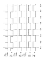
図6に従来のこうしたディスプレイのブロック図を示す。同図において、1−1はアナログの画像信号の入力端子であり、1−2は入力信号の水平同期信号(IHD)入力端子であり、1−3は入力信号の垂直同期信号(IVD)入力端子である。2はADコンバータであり、入力端子1−1に入力されるアナログの画像信号をnビットのデジタル信号に変換する。3は入力系画像処理部、4はメモリ制御部、5は画像データを格納するメモリ部、6は出力系画像処理部であり、7は画像表示部である。20−1、20−2、20−3、20−4は各部へnビットのデジタル信号を伝送するデータバスである。21はメモリの制御線およびアドレス線から構成される制御バスであり、22はメモリのデータバスである。
【0004】
また、8はPLL(Phase Locked Loop)回路であり、ICKは入力IHDに同期した入力系クロックである。12は発振回路であり、出力系クロックOCKを発生する。11はHおよびVカウンタ回路であり、出力系クロックOCKから出力系水平同期信号OHDおよび垂直同期信号OVDを作成する。9はマイクロコンピュータ(μCOM)部であり、19は各部を制御するm本の制御バスである。
【0005】
デジタル画像信号はメモリ部5に格納される前に入力系画像処理部3で画質の調整や画像の縮小変換等の処理を行なわれ、メモリ制御部4に転送される。メモリ制御部4では入力同期信号(IHD、IVD)と入力系クロックICKに対応したタイミングでメモリ部5に画像データを格納するとともに、出力系のクロックOCK、水平同期信号OHDおよび垂直同期信号OVDのタイミングで画像データをメモリ部5から読み出し出力系画像処理部6にデータを転送する。画像処理部6では、画質の調整や、画像の拡大変換などが行なわれる。これにより、入力系の様々なフォーマットの入力画像をメモリを介在して画像表示部7に適したフォーマットの画像信号に変換している。
【0006】
さらに、最近、ワイド対応のテレビやプラズマディスプレイ、リア型プロジェクションTVや投射型のプロジェクターなどの大画面の表示装置において、映画やTV、ホームビデオ、プレゼンテーション、TV会議、各種資料の表示などのさまざまな映像ソースをオフィスや家庭で利用する場面が増加している。さらに、このような形態のなかで、1つの画面内に複数の異なる入力ソースの画像を画面内に分割して表示を行なうマルチ画面表示の表示装置がある。
【0007】
図13に従来こうした場面で用いられるディスプレイの例として、1系統はデジタルのコンピュータ画像信号の入力であり、もう1系統はアナログのコンピュータ画像信号の入力である2系統のPC入力を有し、フレームメモリの出力を制御して合成を行ない、1系統の画像表示部に2画面のマルチ画面表示を行なう画像表示装置の画像処理部のブロック図を示す。
【0008】
図13において、1−1aは1系統目(PC1)のqビットのデジタルのコンピュータ画像信号(IDATA1)の入力端子である。ここでは、本来、赤、青、緑(RGB)の3系統あるはずであるが、構成の説明を簡単にするため、1系統で示している(以下同様)。1−1bは入力信号の水平同期信号(IHD1)入力端子であり、1−1cは入力信号の垂直同期信号(IVD1)入力端子である。1−1dは画像信号のクロック(ICK1)入力端子であり、1−1eは、DDC(DDC1)入出力端子である。20−1a−1、20−1a−2は各部へqビットのデジタルの画像信号を伝送するデータバスである。また、20−1b、20−1c、20−1d、20−1eは、それぞれ、IHD1、IVD1、ICK1、DDC1の信号線である。
DDCとは、標準化団体であるVESA(Video ElectronicStandard Association)が勧告した、コンピュータが表示装置を認識および制御するための通信手段の標準である。
【0009】
1−2aは、2系統目(PC2)のアナログのコンピュータ画像信号(IDATA2)の入力端子である。1−2bは入力信号の水平同期信号(IHD2)入力端子であり、1−2cは入力信号の垂直同期信号(IVD2)入力端子である。1−2eはDDC(DDC2)入出力端子である。
2はADコンバータであり、アナログの画像信号(IDATA2)をnビットのデジタル信号に変換する。また、8はPLL回路であり、端子1−2bから入力した水平同期信号(IHD2)に同期したPC2側の入力系のクロック(ICK2)を発生する。
【0010】
20−2a−0はアナログの信号線であり、20−2a−1、20−2a−2はnビットのデジタルの信号線である。また、20−2b、20−2c、20−2d、20−2eは、それぞれ、IHD2、IVD2、ICK2、DDC2の信号線である。
【0011】
3−1はPC1の入力系の画像処理部であり、3−2はPC2の入力系の画像処理部である。4は2系統の入力画像処理部から入力された画像信号を、一旦メモリに記憶し、マルチ画面として出力するために、画像を合成して出力系の画像処理部に出力する制御を行うメモリ制御部である。5−1、5−2は入力系PC1、PC2にそれぞれ対応したフレームメモリ(メモリA、メモリB)である。21−1、21−2はそれぞれメモリA、Bの制御バスであり、22−1、22−2はそれぞれメモリA、Bのデータバスである。
【0012】
9は、システムを制御するマイコン部であり、19−1および19−2はマイコンから各部への制御線およびデータ線からなるマイコンバス(MB)である。
12は発振回路であり、出力系のクロック(OCK)を発生する。
11はH、Vカウンタ回路であり、出力系のクロック(OCK)をカウントして、出力系の水平同期信号(OHD)と垂直同期信号(OVD)を作成する。
【0013】
また、6は出力系の画像処理部であり、7は液晶やプラズマディスプレイ、CRTなどの画像表示部である。
1−fは画像表示用デジタルデータ(ODATA)の画像表示部の入力端子であり、1−gは出力信号の水平同期信号(OHD)の画像表示部の入力端子であり、1−hは出力信号の垂直同期信号(OVD)の画像表示部の入力端子である。1−iは、出力画像信号のクロック(OCK)の画像表示部の入力端子であり、1−jは、マイコンバス(MB)の画像表示部の入力端子である。
【0014】
また、20−f−1、20−f−2、20−f−3はkビットのODATAの信号線である。20−g−1、20−g−2はOHDの信号線である。20−h−1、20−h−2はOVDの信号線である。20−i−1、20−i−2はOCKの信号線である。
【0015】
画像の入力端子1−1aから入力したデジタル画像信号は、5−1のメモリ部Aに格納される前に3−1の入力系画像処理部1で画質の調整や画像の縮小変換等の処理を行なわれてから、4のメモリ制御部に転送される。
また、画像の入力端子1−2aから入力したアナログ画像信号は、PLL回路8で作成されたクロックに同期して、ADコンバータ2でデジタルデータに変換される。こうして得られたデジタル画像信号は、5−2のメモリ部Bに格納される前に3−2の入力系画像処理部2で画質の調整や画像の縮小変換等の処理を行なわれてから、4のメモリ制御部に転送される。
【0016】
メモリ制御部4では、IDATA1を処理した信号に基づき、入力同期信号(IHD1、IVD1)と入力系クロックICK1に対応したタイミングで5−1のメモリ部Aに画像データを格納するとともに、IDATA2からデジタルに変換された信号を、入力同期信号(IHD2、IVD2)と入力系クロックICK2に対応したタイミングで5−2のメモリ部Bに画像データとして格納する。さらに、出力系のクロックOCK、水平同期信号OHD、垂直同期信号OVDに同期した所定の画像の大きさ、表示位置の関係に合ったタイミングで2つの画像データをメモリ部5−1と5−2から読み出して、出力系画像部6にデータを転送する。画像処理部6では、画質の調整や、画像の拡大変換などが行なわれる。これにより、入力系の様々なフォーマットの入力画像をメモリを介在して画像表示部7に適したフォーマットの画像信号に変換するとともに、2入力から入力された画像データを1画面上に合成してマルチ画面表示を行なう。
【0017】
図7に、図6および図13のディスプレイにおいて、画像表示部7の解像度がXGA(横1024画素×縦768画素)、表示垂直周波数が75Hzである場合に、入力信号(図6の入力信号または図13のPC1入力もしくはPC2入力)として▲1▼VGA(横640画素×縦480画素)100Hz、および▲2▼SVGA(横800画素×縦600画素)60Hzの画像信号が入力された場合の動作タイミングの例を示した。図7の説明上、図13の装置に関してはPC1入力の系統もPC2入力の系統も同様の動作のため、同じこととして説明する。
【0018】
図7において、30、31および32は入力がVGA100Hzの時の入力系の垂直同期信号IVD(IVD、IVD1またはIVD2)、水平同期信号IHD(IHD、IHD1またはIHD2)およびクロックICK(ICK、ICK1またはICK2)を示す。IVDは1周期が1/100secであり、かつブランキング期間の分α1を含んだ、IHDの(480+α1)本分の期間である。また、IHDの1周期は、ブランキング期間の分β1を含んだ、ICKの(640+β1)CLK分の期間である。
【0019】
33、34および35は入力がSVGA60Hzの時のIVD(IVD、IVD1またはIVD2)、IHD(IHD、IHD1またはIHD2)およびICK(ICK、ICK1またはICK2)を示す。IVDは1周期が1/60secであり、かつブランキング期間の分α2を含んだ、IHDの(600+α2)本分の期間である。また、IHDの1周期は、ブランキング期間の分β2を含んだ、ICKの(800+β2)CLK分の期間である。
【0020】
36、37および38は出力がXGA75Hzの時の出力系の垂直同期信号OVD、水平同期信号OHDおよびクロックOCKを示す。OVDは1周期が1/75secであり、かつブランキング期間の分α3を含んだ、OHDの(768+α3)本分の期間である。また、OHDは1周期がブランキング期間の分β3を含んだ、OCKの(1024+β3)CLK分の期間である。
【0021】
このように、入力系の水平同期信号、垂直同期信号および入力クロックは解像度によって異なる周期を持つ。図6の装置において、マイコン部9はこのIHD、IVDなどから解像度やフォーマットを判別してPLL回路8の分周比を設定し、それぞれのフォーマットに相当したICKを発生させる。一方、出力系は入力系の信号とは非同期で、出力クロックOCKからカウンタ回路11で一定のカウンタ値で作成されたOHD、OVDで動作する。このようにして、入力系と出力系の垂直周波数つまり、画面の更新周波数(フレームレート)の変換が行なわれる。
【0022】
図13の装置においては、入力系1(PC1入力)の場合、IHD1、IVD1、ICK1に同期させて、入力の信号処理系を動作させ、メモリAに記録する。入力系2(PC1入力)の場合は、まず、マイコン部9が、このIHD2、IVD2やDDC2でやりとりする情報により解像度やフォーマットを判別して、PLL回路8により、それぞれのフォーマットに相当したICK2を発生させる。次に、IHD2、IVD2、ICK2に同期させて、入力の信号処理系を動作させて、メモリBに画像の記録を行う。
【0023】
一方、出力系は入力系の信号とは非同期で、出力クロックOCKからカウンタ回路で一定のカウンタ値でOHD、OVDの作成を行ない、メモリAおよびメモリBからOCK、OHD、OVDに同期したタイミングで2系統の画像が読み出されるとともに、合成され、出力系の画像処理部および画像表示部に送られる。このようにして、入力系と出力系の解像度変換および垂直周波数つまり、画面の更新周波数(フレームレート)の変換が行なわれる。
【0024】
【発明が解決しようとする課題】
しかしながら、このフレームレート変換においては、図8に具体例を示すような動画像の画質劣化の問題点が存在する。図8の説明においても図13に関しては、PC1入力の系統もPC2入力の系統も同様の動作のため、同じ現象が生じる。ここでは、入力の垂直周波数と出力の垂直周波数の比が5:4の場合(例えば100Hzと80Hzなど)を例として示す。図8において、41は入力される連続した5枚(a〜e)のフレーム画像、42は同じ期間に表示装置に出力される連続した4枚(f〜1)のフレーム画像である。矢印が画面左から右方向へ移動する動画を表示している。
【0025】
同じメモリ領域に1画面を書き込みながら読み出しているため、(a)と(f)、(e)と(i)のようにたまたま1画面を書き換えるタイミングと読み出すタイミングが近い時は画面上に変化は現れないが、(g)、(h)のように画面を読み出している途中で画面が書き変わるタイミングになると、1画面の途中で前後の画面が切り替わり、動いている画像が画面の上下でずれてみえてしまう。これは“画像の追い越し”とよばれ、動画を表示する場合の画像の品位が落ちてしまう現象である。これは、逆に出力の垂直周波数が入力の垂直周波数より速い場合も同様の現象として現れる。
【0026】
この現象は、比較的画面に対して大きめな幾何学的な物体が水平に平行移動している時に目立ちやすいが、自然画などではあまり目立ちにくく、また、従来のPCはワープロ、表計算、描画といった静止画の用途が多いため、大きな問題にはならなかった。しかしながら、前述したようにPCといえども最近は動画を表示する機会が多くなり、また、幾何学的なグラフィックの移動する画面も多くなってきたため動画に対する要求も高くなってきている。
【0027】
このような問題の対策として、ダブルバッファリングという方法がある。これは、メモリ領域を1画面分ではなく、2画面分用意して1画面おきに交互にメモリ領域を切り換えて書き込むとともに、読み出しは画面の追い越しが起きないように、必ず読み出しているメモリ領域の走査が、そのメモリ領域の書込みの走査より先行する関係となるようにメモリ領域を選択するように制御する方法である。
【0028】
例えば、XGA(1024×768)の画素数のデータを格納する場合、図9のメモリマップに示すようにアドレス00000h〜BFFFFhの第1のメモリ領域にm、m+2、m+4・・・フィールドといった偶数番目のフィールドの入力画像を格納し、C0000h〜17FFFFhの第2のメモリ領域にm+1、m+3、m+5・・・フィールドといった奇数番目のフィールドの入力画像を格納する。図10にこの時のメモリの書込みと読み出しの動作のタイミングチャートを示す。61に入力の垂直同期信号(IVD)を、64に出力の垂直同期信号(OVD)を示す。ここでの説明も図13に関してはPC1入力とPC2入力に共通するので、IVDはIVD1またはIVD2(もしくは両方)を示し、また第1のメモリ領域と第2のメモリ領域はメモリAまたはメモリB(もしくは両方)にそれぞれ設けられると仮定する。
【0029】
IVD61が入る度にm、m+1、m+2・・・というように入力フィールドが更新され、またOVD64が入る度にn、n+1、n+2・・・というように出力フィールドが更新される。62に第1のメモリ領域の書込みが行なわれることを示す信号(WE1)を、63に第2のメモリ領域の書込みが行なわれることを示す信号(WE2)を、65に第1のメモリ領域の読み出しが行なわれることを示す信号(RE1)を、63に第2のメモリ領域の読み出しが行なわれることを示す信号(RE2)を示す。ここでは、アクティブHighで示す。
【0030】
書込みは前述したように、入力フィールドの偶数番目と奇数番目で交互に第1と第2のメモリ領域に書き込まれるが、読み出しは書込み途中が表示されないフィールドを選択して読み出されている。ここでは、入力に対して出力側が垂直周波数が高いので出力VDがHighになった時の入力フィールドが第1のメモリ領域を書き込んでいる場合、第2のメモリ領域を読み出し、第2のメモリ領域を書き込んでいる場合、第1のメモリ領域を読み出すように制御して、追い越し現象が現れないようにしている。出力側の垂直周波数が低い場合は、入力のVD(IVD)と出力のVD(OVD)の関係をみながら、追い越しが起きないように制御する必要がある。いずれにしても、第1のメモリと第2のメモリの読み出しタイミングは入力と出力の周波数や、同期信号間の関係にあわせて、必ず読み出しているメモリ領域の走査が、そのメモリ領域の書込みの走査より先行する関係となるようにメモリ領域を切り換えるように設定される。
【0031】
しかしながら、このダブルバッファリング方式においても、以下に示すような動画上の問題点がある。
ダブルバッファリングの場合、現在書込み途中のメモリ領域を表示しないように、もう一方のメモリ領域を選択することから、例えば図11のように、入力画面71(a)〜(d)の、人が片手をまわしているような連続した動きの画面がある場合に、72(e)〜(i)のようにフレームレートを変換された出力のうち(e)と(f)のように、同じ画像が2フィールド連続する“フレームの二重化”や、図12のように、入力画面81(a)〜(d)のような画面がある場合に、82(e)〜(g)のようにフレームレートを変換された出力のうち(c)のように、相当するフィールドがなくなる“フレームの欠落”が生じてしまう。
【0032】
また、ダブルバッファリングとは別の方法で動画質を改善する方法としては、入力の垂直周波数と出力の垂直周波数を同期させる方法がある。XGA(1024×768画素)の表示部の場合、VGA(640×480)やSVGA(800×600)などの50Hzの入力信号が入ってきた場合はXGA50Hzに変換して表示を行ない、また、100Hzの入力信号が入ってきた場合はXGA100Hzに変換して表示を行なう方法である。
【0033】
こうした場合、メモリの書込みと読み出しの周期が一致するため、動きの問題点は発生しない。ところが、入力の信号源が50Hzなど低い周波数の場合は、液晶のようにフィールド毎に極性を反転して表示している装置などの場合、同じ極性でみるとさらに半分の周波数となるため、画面の書き換え周期が遅くなり、面全体がちらついてみえるフリッカ現象となってしまう画質上の問題がある。また、100Hzのように速い周波数になると、VGAのように画素数が低い場合には大した速度でなくても、XGAの画素数の出力に変換すると入力の2.6倍程度のスピードが要求されるため、出力系全体の動作速度を高くしなくてはならない問題点がある。例えば、XGAの60Hzでは65MHz程度のクロックレートのものが、XGA100Hzでは108MHz程度となり、100MHzを越えてしまう。解決のためには、高い動作速度の部品の採用や新規な部品の開発、動作系統を分割して速度を下げるなどの回路構成にする必要などがあり、コストの上昇や回路規模の増大につながってしまう。
【0034】
上記の問題に加えて、入力が2系統以上であることゆえの問題点も存在する。図13の例で示したように、入力系はそれぞれの入力信号と同期して動作するため、PC1入力とPC2入力は基本的に非同期である一方で、出力系は同一のタイミングで2系統の画像を1画面に合成して出力するために、入力と出力の垂直周波数を同期させる方法はどちらか1系統に対しては実施できるが、同時に2系統に対しては適用できない。この問題は、入力系統が増加し、それぞれの動画の画質を重視するマルチ画面用途に対して大きな問題になる。
【0035】
さらに、複数の画像入力に対しては、動画の画質同様に、色や明るさ、コントラストなど、様々な画質特性面でマルチ画面特有の、いずれか1系統の入力系にしか最適化できないか、もしくは最適化する場合回路規模が増大する問題が発生する。
【0036】
ここで、画像のコントラストやブライト、ガンマ特性など画質の階調性に関わる問題の例を図13の回路で示す。
図14は、図13などの画像処理装置に入力する映像信号の1つとして水平方向に階調が8段階に変化するグレースケール信号を示す。14−1はグレースケールでの表示画面であり、14−2はこの時の信号である。14−2において、横軸は1水平走査期間の時間であり、縦軸は信号レベルである。14−3はこのときの入力信号の水平同期信号である。ここでは、1水平期間に、0%から100%までを8段階に等分に変化している。
【0037】
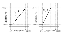
また、図15に、図13の画像表示部7における入力信号に対する表示画面の輝度特性を示す。この特性は、例えば透過型の液晶であれば、入力電圧に対する光の透過率特性であり、反射型のデバイスであれば、入力電圧に対する光の反射率特性である。この特性は、図13の画像表示部7によって適した特性が異なる。ここでは、15−1、15−2の2種類の特性を例に挙げて説明する。15−1、15−2において、横軸は画面表示部の入力信号のレベル、縦軸は表示輝度のレベルであり、イ、ロ、ハはそれぞれ入力信号のあるレベルを示している。
【0038】
ここで、図13のPC1、PC2の2系統の入力IDATA1、IDATA2に対して、それぞれ図16に示す16−1A、16−1Bのように信号レベルの異なる入力信号が入力されたとする。
また、図16には図15に15−1で示す特性の画像表示部を用いた場合の2系統の信号での表示輝度レベル16−4Aおよび16−4Bを示す。16−4A、16−4Bに示すように、同様の階調数の入力信号でもIDATA2の16−4Bが白100%黒0%がつぶれているものの、ほぼ輝度レベルとしては0%から100%まで出ているのに対して、もう一方の16−4Aは黒が60%程度まで白側にシフトし白く浮いた画像になっている。このため、同一の表示装置に2つの画面を同時表示すると、異なる黒レベルで、かつ、コントラストの異なる2つの画面が混在するため、非常に見づらい画面表示になる。
【0039】
ここで、図13の入力系画像処理部1(3−1)および入力系画像処理部2(3−2)にAGC(Auto−Gain−Control)回路を持たせた場合は、入力信号の直流レベルと振幅の異なる信号に対しては補正が行なわれる。しかし、ここで、画像表示部が図15の15−2の特性を有する表示部に交換された場合、この特性の変化に対しては信号の補正が行われない。
【0040】
図17および図18に、表示部の特性が図15の15−1の場合と15−2の場合の入力信号と輝度レベルを示す。図17および図18において、2系統の入力IDATA1およびIDATA2に入力する入力信号16−1A、16−1Bと、入力系画像処理部1(3−1)および入力系画像処理部2(3−2)のAGC回路通過後の各信号レベル16−2A、16−2B、およびこの信号を入力したときの表示部の輝度レベル16−4A、16−4Bを示す。図17の16−4A、16−4Bに示すように、15−1の入出力特性ではAGCにより階調は0%から100%まで出ている。
しかし、図18の16−4A、16−4Bに示すように、15−2の入出力特性では階調は0%から60%までしかでていなく、白側数段階が白つぶれ画像になってしまう。
【0041】
このような、画像表示部の特性の交換に対しては、図13の出力系画像処理部6に、画像表示部の特性に対する補正特性を持たせることが考えられる。図19に、表示部の特性が図15の15−2の場合の入力信号と輝度レベルを示す。2系統の入力IDATA1およびIDATA2に入力する入力信号16−1A、16−1Bと、入力系画像処理部1(3−1)および入力系画像処理部2(3−2)のAGC回路通過後の各信号レベル16−2A、16−2Bに加えて、出力系画像処理部通過後の各信号レベルを16−3A、16−3Bに、この信号を入力したときの表示部7の輝度レベルを16−4A、16−4Bに示す。
【0042】
このように、各信号の入力系画像処理部に入力信号の補正特性を持ち、出力系画像処理部に表示部の補正特性を持たせることにより、各入力信号のレベル差や、表示部の特性ばらつきの影響の少ないマルチ画面表示が実現される。補正特性としては、明るさ(ブライト)、明暗(コントラスト)、ガンマ特性、およびそれらの各色の系での差から生じるホワイトバランスなどがある。
【0043】
しかしながら、このように、入力系と出力系の両方に画像信号の補正特性を設けることは、同様の回路を複数用意することになり、回路規模、調整項目数が増加し、コストの増大を招く。これは、特に入力数が多い構成において問題になる。
さらに、こうした構成は、特性補正のためのデジタル処理系を2回以上通すことにより、画像の劣化も招く。図20に、この説明のための概念図を示す。図20において、x軸は入力信号のレベルを、y軸は出力信号の入力レベルを示す。この図では8ビット256段階のデジタル処理系での、▲1▼y=xの入出力特性に対して、▲2▼y=x2 の特性1のテーブルと▲3▼y=x1/2の特性2のテーブルを通過させた後の▲4▼y=[x2 ]*[x1/2]≒xの入出力特性を示している。本来であれば、▲4▼と▲1▼は一致するはずであるが、▲2▼の特性1と▲3▼の特性2の演算通過の各段階で出力は8ビットに規格化されるため、その度に演算誤差が発生して、合成後の▲4▼では、0から50程度のxに対してのyのビット誤差が大きくなっている。
【0044】
こうしたことを、従来例に当てはめて考えると、入力系で▲2▼のような特性変換を与えて、出力系で▲3▼のような特性変換を与えることに相当し、この場合、出力画像の黒レベルの階調性が劣化し、画像に疑似輪郭のような画質劣化が生じることになる。
この現象を避けるために、演算ビットを増加させる方法もあるが、コストや処理系の規模の増大を招く。
【0045】
このように、従来、複数の入力信号源の画像を同じ表示部に表示するマルチ画面表示において、表示部の特性の変化に対して、異なる入力画像の特性を同じ表示特性に変換する構成は規模が大きくなりコストが増大する問題があった。また、回路構成上ビット誤差の大きな回路となり、画質劣化を招く問題を有していた。このため、容易に各入力系統の明るさやコントラスト、階調性、色などを揃えられなかった。
【0046】
また、AGC回路を入力画像処理装置に持たせた場合は、信号のダイナミックレンジは確保できるが、自動で補正をするため、本来表示すべき信号レベルまでも補正を行い、信号送出側の意図を無視してしまう問題も存在した。
【0047】
本発明の目的は、安価かつ簡単な回路構成で動画像の画質を改善した画像処理装置を実現することにある。また、複数の入力信号源に対しても、柔軟に動画質に対して適した処理を行なえる画像処理装置を実現することにある。
【0050】
【課題を解決するための手段および作用】
上記の目的を達成するため本発明に係る第1の画像処理装置は、少なくとも1画面分の画像を記憶する記憶領域を有するメモリ部と、第1のクロックと第1の画像同期信号により、このメモリ部へ画像データを書き込むための入力系の動作を行ない、第2のクロックと第2の画像同期信号により、このメモリ部から読み出した画像データを出力する出力系の動作を行なうメモリ制御部と、前記第2のクロックを作成するクロック発生部と、第2のクロックを入力し前記第2の画像同期信号を出力する同期制御部とからなる画像処理装置において、前記同期制御部は、第2のクロックを分周して、第1の画像同期信号とは非同期の第3の画像同期信号と、第2のクロックにより、第1の画像同期信号を同期化して作成した第4の画像同期信号を作成するとともに、前記第3の画像同期信号と前記第4の画像同期信号を切り換えて、前記第2の画像同期信号として出力することを特徴とする。これらの第3の画像同期信号と前記第4の画像同期信号の切り換えは、出力する画像の使用目的に応じて選択される。
【0051】
本発明は、複数の入力系信号処理部を有し、そこに入力される画像信号を適宜合成して表示する場合にも適用可能である。本発明に係る第2の画像処理装置は、第1の画像同期信号に同期する第4の画像同期信号として、複数の第1の画像同期信号のそれぞれに同期する複数の第4の画像同期信号を作成し、作成した複数の第4の画像同期信号と第1の画像同期信号とは非同期の第3の画像同期信号の中から1つの画像同期信号を選択し、前記第2の画像同期信号として出力する。第2の画像同期信号となる画像同期信号は、出力する画像の使用目的、または前記複数の入力系信号処理部に入力する信号の動画の有無や割合、あるいは前記複数の入力系信号の用途や種類に応じて、前記第3の画像同期信号と前記第4の画像同期信号群の中の1つを選択する。この第2の局面においては、さらに、前記複数の入力系信号処理部に入力する信号源に対して、入力する画像信号を設定、あるいは再設定する要求を出力する手段を設け、前記第3の画像同期信号と前記第4の画像同期信号群の中から選択して出力する第2の画像同期信号に同期していない任意の入力信号源に対して、第2の画像同期信号に同期する要求を出力する構成とすることが好ましい。 本発明に係る第3の画像処理装置は、複数の入力系信号処理部と、少なくとも1画面分の画像を記憶する記憶領域を有するメモリ部と、前記複数の入力系信号処理部に入力される複数の入力信号に同期した複数の第1のクロック群と第1の画像同期信号群を用いて、このメモリ部へ画像データを書き込むための入力系の動作を行ない、第2のクロックと第2の画像同期信号により、このメモリ部から読み出した画像データを出力する出力系の動作を行なうメモリ制御部と、前記第2のクロックを作成するクロック発生部と、第2のクロックを入力し前記第2の画像同期信号を出力する同期制御部からなる画像処理装置において、前記同期制御部は、第2のクロックから分周され、第1の画像同期信号群とは非同期の第3の画像同期信号と、第2のクロックにより、第1の画像同期信号群をそれぞれ同期化して作成した第4の画像同期信号群を作成するとともに、前記第3の画像同期信号と前記第4の画像同期信号群の中から一つの画像同期信号を選択して、前記第2の画像同期信号として出力し、前記画像処理装置は、前記複数の入力系信号処理部に入力する信号源に対して、入力する画像信号を設定、あるいは再設定する要求を出力するとともに、前記第3の画像同期信号と前記第4の画像同期信号群の中から選択して出力する第2の画像同期信号に同期していない任意の入力信号源に対して、第2の画像同期信号に同期する要求を出力する手段を有することを特徴とする。
【0052】
本発明は、CRTをはじめ透過型、反射型の表示装置、液晶表示装置、PDP(プラズマディスプレイ)や電荷放出型表示装置などの画像表示装置、CCDやCMOS型の2次元撮像素子、およびビデオ信号のキャプチャーボード等のデジタル画像処理を伴なうあらゆる画像処理装置に適用可能である。
【0057】
【実施例】
以下、本発明の実施例について、図面を用いて説明する。
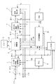
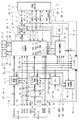
(実施例1)
本発明の第1の実施例の説明のためのブロック図を図1に示す。同図において、1−1はアナログの画像信号の入力端子であり、1−2は入力信号の水平同期信号(IHD)入力端子であり、1−3は入力信号の垂直同期信号(IVD)入力端子である。2はADコンバータであり、入力されたアナログ画像信号をnビットのデジタル信号に変換する。3は入力系画像処理部、4はメモリ制御部、5は画像データを格納するメモリ部、6は出力系画像処理部であり、7は画像表示部である。20−1、20−2、20−3、20−4は各部へnビットのデジタル信号を伝送するデータバスである。21はメモリの制御線とアドレス線から構成される制御バスであり、22はメモリのデータバスである。
【0058】
また、8はPLL回路であり、ICKは入力水平同期信号IHDに同期したクロックである。12は発振回路であり、出力系クロックOCKを発生する。9はマイクロコンピュータ(μCOM)部であり、19はm本の、各部を制御する制御バスである。
【0059】
デジタル画像信号はメモリ部5に格納される前に入力系画像処理部3で画質の調整や画像の縮小変換等の処理を行なわれ、メモリ制御部4に転送される。メモリ制御部4では入力同期信号(IHD、IVD)と入力系クロックICKに対応したタイミングでメモリ部5に画像データを格納するとともに、出力系クロックOCK、水平同期信号OHD、垂直同期信号OVDのタイミングで画像データをメモリ部5から読み出し、出力系画像処理部6にデータを転送する。画像処理部6では、画質の調整や、画像の拡大変換などが行なわれるのは図6の従来例と同様である。
【0060】
図1においては、10が同期制御部であり、出力のフレームレートを決定するブロックである。ここには、入力の同期信号IHD、IVDと出力系クロックOCKが入力し、出力系の水平同期信号OHD、垂直同期信号OVDと書込みフィールド制御信号WEと読み出しフィールド制御信号REを出力する。また、これらの制御をマイコンのバス19によりコントロールする。
【0061】
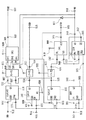
図2にこの同期制御部10の回路構成例を示す。
図2において、901はOCKをカウントするHカウンタであり、902はOHDをカウントする第1のVカウンタであり、904はIHDをカウントする第2のVカウンタであり、905、906、907はカウンタ901、902、904それぞれの出力をデコードして任意のパルスを作成する第1、第2、第3のデコーダである。903と910はD入力フリップフロップ(D−FF)である。また、908および909は入力のパルスを切り換えて出力する第1および第2のスイッチ(SW1およびSW2)である。また、911は論理を反転するインバータである。また、912がIHDの、913がIVDの、914がOCKの入力端子であり、915がOHDの、916がOVDの、917がREの、918がWEの出力端子である。また、919、920がマイコンの制御バスのうち、各SWを切り換える信号線の入力端子であり、921、922、923は第1〜第3のデコーダの値を設定するためのマイコンの制御バスの入力端子である。
【0062】
925、926、927は各カウンタのクロック入力端子であり、930、931、932は各カウンタのクロックのイネーブル端子であり、934、935、936は各カウンタの出力端子である。950はHカウンタのリセット端子である。また、出力端子934、935、936、937は各デコーダの入力端子にも接続しており、938、939、940は各デコーダの出力端子である。
【0063】
928、929は各D−FF903、910のクロック端子であり、933はクロックのイネーブル端子、941、942はD−FFの入力端子である。また、943、944はD−FFの非反転出力端子であり、952は反転出力端子である。
【0064】
947、948は第1のスイッチ908の入力端子IN1、IN2であり、949は出力端子である。940、945、946は第2のスイッチ909の入力端子IN3、IN4、IN5であり、951は出力端子である。
【0065】
ここで、Hカウンタ901とデコーダ905でOCKをカウントおよびデコードしてOHDを作成し、915から出力するとともに、作成したOHDを第1のVカウンタ902とデコーダ906でカウントおよびデコードして第1のスイッチの入力端子947に結果を出力する。一方、入力したIVDはD−FF903を通過し、第1のスイッチ908の入力端子948に入力する。入力端子947と948に入力した信号は、端子919に入力されるマイコンからの制御信号により動作モードによって選択、切り換えされて、どちらか一方が端子916にOVDとして出力される。
【0066】
また、D−FF903の出力はD−FF910のイネーブル端子933にも入力し、端子933にIVDが入力する度に極性が反転するメモリ書き込み信号WEを端子918に出力する。また、このメモリ書き込み信号WEとその反転論理信号とが、メモリ読み出し信号の候補信号として第2のスイッチ909の入力端子945、946に入力する。さらにIHDのカウンタ904とOHDのカウンタ902との両者の出力結果をデコーダ907でデコードして、両者の関係で定まる信号もメモリ読み出し信号の候補信号として第2のスイッチ909の入力端子940に入力し、端子920へのマイコンからの制御信号にしたがって、動作モードによってこの3入力の1つが選択されて、メモリ読み出し信号REとして端子917から出力される。
【0067】
この実施例における、入力信号の周波数に対する動作モードと第1および第2のスイッチの切り換えて出力される信号との対応表を表1に、またその時のタイミングチャートを図3に示す。
【0068】
【表1】

表1には、入力信号の垂直周波数の範囲に対して、出力の垂直周波数が入力信号に同期しているかどうかと、ダブルバッファリングするかどうか、およびその動作を実現するための図2におけるSW1、SW2の切換出力する信号を示している。
【0070】
また、図3においてA1、A2、A3、A4、A5はそれぞれ入力垂直周波数が100Hz、80Hz、75Hz、60Hz、50Hzのときの入力垂直同期信号IVDであり、A6、A7は入力周波数が80Hzのときの出力垂直同期信号と出力水平同期信号である。A8、A9は入力周波数が75Hzのときの出力垂直同期信号と出力水平同期信号である。A10、A11は入力周波数が60Hzのときの出力垂直同期信号と出力水平同期信号である。A12、A13は入力周波数が50Hzのときと100Hzのときの出力垂直同期信号と出力水平同期信号である。
【0071】
本実施例では、使用頻度の高い60Hzから80Hzまでの垂直周波数の入力信号に対応して出力の垂直同期信号OVDを入力の垂直同期信号IVDに同期させるモードを、それ以外の入力信号については、入力の垂直同期信号には無関係に出力の垂直同期信号を発生させるモードを選択する構成をとっている。
【0072】
このため、60Hzから80Hzまでの垂直周波数の入力信号に対応しては、ダブルバッファリングを用いず(用いてもかまわない)、入力の垂直同期と同期させる方法で動画に対して追い越し、フレームの二重化、および欠落のない画質を実現している。このとき、第1のスイッチはIN2側、第2のスイッチはIN5(IN4でも可)を選択する。
【0073】
また、60Hz未満の場合は、フリッカ防止のため、SW1をIN1側としてダブルバッファリングによる動画質の改善を行ない、入力に対しては非同期とする。入力の垂直周波数が出力の周波数より低い場合は、書込みメモリ領域と反対のメモリ領域を読み出しフィールドとすればメモリ読み出し走査を書込み走査が追い越すことはないので、SW2をIN4側としている。
【0074】
一方、80Hz以上では出力系の動作スピードを抑えるために、SW1をIN1側としてダブルバッファリングによる動画質の改善を行ない、入力に対しては非同期とする。入力の垂直周波数が出力の周波数より高い場合は、書込みメモリ領域と反対のメモリ領域を読み出しフィールドとしても、メモリ読み出し走査を書込み走査が追い越すことがあるので、SW2をIN3側として、入力のIHDと出力のOHDの関係から追い越しが生じないタイミングでメモリ読み出し信号を出力している。
【0075】
このとき、図1の発振器(OSC)12の周波数は、出力系の最高垂直周波数であるXGA80Hzの時のクロック周波数にあわせて設計される。すなわち、1フィールド=1V期間=1S/80=12.5mSであるから、例えば、1V=(768+α)H=808Hとして1H期間=15.5μS、1H=(1024+α)CLK=1344CLKとして1CLK=11.5nSとなり、発振器12の周波数は、1/11.5nS=87MHzとなる。図3において、A2の80HzのIVDが入力した場合、その出力OVD=IVDとなり、OVDの1周期間のIHDは768+α=808個に設定される。
【0076】
また、A3、A4の75Hz、60HzのIHDが入力した場合、対応するOHDであるA8、A9はIHDと同周期になり、また、OVDの1周期間のOCKおよびOHDの周期は一定に保たれるため、OVD1周期間のOHD数が比例して増加する。この768+α=808本を越える分の期間についてはブランキング期間が増加すると考えて表示部を駆動している。
【0077】
一方、入力IHDが100HzのA1や50HzのA5の場合は、入力と非同期に出力の垂直周波数を設定するため、A12のOVD、A13のOHDに示すように80Hzの時と同じOVD、OHD周期でかつ、入力と非同期に自走させている。60〜80Hzという周波数は、現行のPCやWS(ワークステーション)やDTV(デジタルテレビ)等、最も広く普及している周波数帯である一方、TVからの動画の映像ソースもNTSCが60Hzのため、この範囲に入ってくるため使用頻度が非常に高く動画を最優先させる意味は高い。
【0078】
一方、50Hzなど、低い周波数のフリッカ現象は、動画、静止画に関らず非常に見づらい画質劣化となる点から、ダブルバッファリングのような簡易的に動画に強い方式をとる方法で、フリッカ防止と動画画質向上を両立させている。
【0079】
また、100Hzのように高い垂直周波数の信号に関しては、100MHzを超える動作速度が回路的な負担が大きいことを重視し、ダブルバッファリングのような簡易的に動画に強い方式をとる方法で、コスト削減と安定動作を動画画質向上と両立させている。特に液晶やPDPなどの表示素子は駆動電圧が10数Vから数十Vという高電圧が必要とされるため、1画素あたりの速度が高速化すると、映像信号系やドライバ回路が非常に高い動作帯域やスルーレートが必要とされる。現状においても、こうした高い速度の駆動に対しては追従できない部分を、複数に分割駆動しているが、さらなる出力系の高速化は高速な部品ヘの変更、新規部品の開発、分割数の変更などの回路変更によるコストアップばかりでなく回路の動作マージンを狭くし、安定的な動作を困難にする要因となる。また、この問題はSXGAやUXGAといった、現状よりもさらに数倍画素数の多い表示素子などを駆動する場合に、特に重要になる。将来の高画素化のためにも、コスト削減と安定動作が動画画質向上と両立できる点が重要になってくる。
【0080】
本実施例のような構成をとることで、システムの全体の動作として、動画に強い構成をとり、特に使用頻度の高い垂直周波数帯で動画の問題のない動作を実現し、また、その他の垂直周波数帯では簡易的に動画に強い動作を行なうことで回路構成の簡素化、安価化を実現している。
【0081】
ここでは、使用頻度の高い垂直周波数帯域以外の周波数をダブルバッファリングさせたが、ダブルバッファリングは、メモリ領域を倍必要とすること、またそのための制御回路部分が必要となるため、機能として省くことも考えられる。特定の垂直周波数帯域は入力の垂直周波数に同期させる一方で、その帯域以外の使用頻度は低いと判断し、製品として動作はするが、動画質は改善しない単なる非同期な動作に切り換えることも安価な製品を提供する意味で本発明のひとつの実施の形態である。
【0082】
また、本実施例では、入力信号の垂直周波数により、出力系を入力系と同期させるか非同期とするかを選択したが、本発明の第1の実施形態は出力系を入力系と同期させるか非同期とするかを選択する回路を有することが特徴であり、切り換える基準は入力信号の垂直周波数以外にも、入力信号のフォーマットのほかの項目であったり、システムの動作モードであったり、ユーザー設定などによる場合も含んでいる。実施例2は、このような基準として、動画か静止画かを選択の基準にした例を示す。
【0083】
(実施例2)
実施例1では、入力信号の垂直周波数によって出力系のV同期を入力同期信号に同期させるか非同期にするかを切り換える例を示したが、実施例2では、動作目的や用途で入力の同期信号に同期させるか非同期にするかを切り換える例を示す。図4に実施例2のブロック図を示す。
【0084】
ここでは、入力系が2系統になり、メモリ制御部で合成している。これは、図5に示すように、例えば画面全体(C1)にPCのグラフや表などの出力画面を表示して、子画面部(C2)にTV電話の画像などの動画を出力するなどの、異なる入力源の合成画面を想定した回路構成である。こうした場合、両者の信号には一般的に同期関係がない。また、動画か静止画かは接続される入力源によって多種多様な組み合わせとなる。
【0085】
図4において3−1は入力A系統の画像処理部であり、1−4はqビットのデジタルの画像信号の入力端子であり、1−5は入力信号の水平同期信号(IHD1)入力端子であり、1−6は入力信号の垂直同期信号(IVD1)入力端子、l−7は入力信号の同期クロック(ICK1)入力端子である。また、3−2は入力B系統の画像処理部であり、1−8はアナログの画像信号の入力端子であり、1−9は入力信号の水平同期信号(IHD2)入力端子であり、1−10は入力信号の垂直同期信号(IVD2)入力端子である。2はADコンバータであり、B系統のアナログ信号をnビットのデジタル信号に変換する。4−2はメモリ制御部、5は画像データを格納するメモリ部、6は出力系画像処理部であり、7は画像表示部である。20−5、20−6はqビットのデジタル信号のデータバスであり、20−7、20−8はnビットのデジタル信号を伝送するデータバスである。また、20−9、20−10はrビットのデジタル信号を伝送するデータバスである。21はメモリの制御線とアドレス線から構成される制御バスであり、22はメモリのデータバスである。
【0086】
さらに、1−11、1−12はそれぞれ入力A系統、B系統のDDC(Display Data Cannel)端子であり、ディスプレイの情報を入力信号源に伝える端子である。なお、DDCは、VESA(Video Electronics Standards Association)により規格化されたコンピュータ用ディスプレイとホストシステム間の通信の標準である。
【0087】
また、8はPLL回路であり、ICK2は入力B系の水平同期信号IHD2に同期したクロックである。12は発振回路であり、出力系クロックOCKを発生する。9はマイクロコンピュータ(μCOM)部であり、19はm本の、各部を制御する制御バスである。
【0088】
デジタル画像信号はメモリ部5に格納される前に入力系画像処理部3−1、3−2で画質の調整や画像の縮小変換等の処理を行なわれ、メモリ制御部4−2に転送される。また、入力系画像処理部3−1、3−2では動き検出も行ない、その結果をマイコンのバス19を介してマイコン9に送る。メモリ制御部4では入力同期信号(IHD1、IHD2、IVD1、IVD2)と入力系クロックICK1、ICK2に対応したタイミングでメモリ部5に画像データを格納するとともに、出力系クロックOCK、水平同期信号OHD、垂直同期信号OVDのタイミングで画像データをメモリ部5から読み出し、出力系画像処理部6にデータを転送する。画像処理部6においては、図6の従来例と同様に、画質の調整や、画像の拡大変換などが行なわれる。
【0089】
図4において、10が同期制御部であり、出力のフレームレートを決定するブロックである。ここには、2系統の入力系同期信号IHD1、IVD1、IHD2、IVD2と出力系クロックOCK18が入力し、出力系の水平同期信号OHDおよび垂直同期信号OVDと、書込みフィールドの制御信号WEと、読み出しフィールド制御信号REとを出力する。また、これらの制御をマイコンのバス19によりコントロールする。
【0090】
ここで、同期制御部10の動作例を表2に示す。実施例1同様、出力の垂直同期信号をスイッチを用いて、入力に同期か非同期かを切り換える。実施例1と異なるのは、入力が2系統になった点と、周波数によって同期関係を切り換えるほかに、入力源2系統の動画と静止画の状態によって同期関係を切り換える点である。
【0091】
【表2】
前述の入力の画像処理部3−1、3−2の動き検出の結果を受けて、マイコン部9からの制御信号により、表2のように動作モードを切り換える。一方が動画で一方が静止画の場合は、動画のほうの入力垂直同期信号にOVDを同期させる。また、2系統とも動画の場合には、IVD1とIVD2を比較し速い周期の垂直同期信号にOVDを同期させる。また、据置のTV会議システムなど、A系統がPCでB系統がTV出力などのように用途が固定している場合には、マニュアル設定でA系統のIVD1に同期させるか、B系統のIVD2に同期させるか、A、Bとも非同期にOVDを発生させるかを決定できるようにしてある。
【0093】
さらに、本実施例では、DDCなどのディスプレイ側の情報をPCなどの入力信号源に伝える制御線を用いて、以下に述べる制御も行なう。すなわち、最初の状態で、一方のみが動作し、一方が接続されていない場合、例えばB系統のみが接続、動作しているとすると、同期制御部10は実施例1同様、IVD2に対してOVDを表1のような動作に設定する。
【0094】
次に、後から1系統が接続される場合に(この場合A系統)、マイコンは現在のOVD周期と同じ垂直周波数の信号をA系統のDDC端子1−11を介し入力信号源に対して要求する。これを受けたA系統の入力信号源は、要求された垂直周波数の信号に設定を行ない、結果として入力の2系統とも同じ周波数となり、両方の画像が動画に対して強い出力設定にすることが可能にできる。
【0095】
また、新規のA系統がDDCを受け付けない場合は、マイコン部が判断を行ない、後に接続されたA系統のIVD1に同期した設定に出力同期OVDを再設定する一方、このOVD周期と同じ垂直周波数の信号をB系統のDDC端子1−12を介してB系統の入力信号源に対して要求する。これを受けたB系統の入力信号源は、要求された垂直周波数の信号に再設定を行ない、入力の2系統が同じ周波数に設定される。
【0096】
このような構成をとることで、複数の異なる周期の入力信号が混在するシステムにおいても、出力系の構成は1系統のクロックで動作させながら、動画に強い構成を簡単で安価な回路構成で実現することができる。
【0097】
(実施例3)
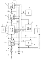
図21は本発明を適用したディスプレイの第3の実施例として、1系統はデジタルのコンピュータ画像信号の入力であり、もう1系統はアナログのコンピュータ画像信号の入力である2系統のPC入力を有し、フレームメモリの出力を制御して合成を行ない、1系統の画像表示部に2画面のマルチ画面表示を行なう画像表示装置の画像処理部のブロック図を示す。
【0098】
同図において、1−1aは1系統めのqビットのデジタルのコンピュータ画像信号(IDATA1)の入力端子である。ここでは、本来、赤、青、緑(RGB)の3系統あるはずであるが、構成の説明を簡単にするため、1系統で示している(以下同様)。1−1bは入力信号の水平同期信号(IHD1)入力端子であり、1−1cは入力信号の垂直同期信号(IVD1)入力端子である。1−1dは画像信号のクロック(ICK1)入力端子であり、1−1eはDDC信号(DDC1)の入出力端子である。20−1a−1、20−1a−2は各部へqビットのデジタルの画像信号を伝送するデータバスである。また、20−1b、20−1c、20−1d、20−1eは、それぞれ、IHD1、IVD1、ICK1、DDC1の信号線である。
【0099】
1−2aは2系統めのアナログのコンピュータ画像信号(IDATA2)の入力端子である。1−2bは入力信号の水平同期信号(IHD2)入力端子であり、1−2cは入力信号の垂直同期信号(IVD2)入力端子である。1−2eはDDC信号(DDC2)の入出力端子である。
【0100】
2はADコンバータであり、アナログの画像信号(IDATA2)をnビットのデジタル信号に変換する。また、8はPLL(Phase Locked Loop)回路であり、1−2bから入力した水平同期信号(IHD2)に同期したPC2側の入力系のクロック(ICK2)を発生する。
【0101】
20−2a−0はアナログの信号線であり、20−2a−1、20−2a−2はnビットのデジタルの信号線である。また、20−2b、20−2c、20−2d、20−2eは、それぞれ、IHD2、IVD2、ICK2、DDC2の信号線である。
【0102】
3−1はPC1の入力系の画像処理部1であり、3−2はPC2の入力系の画像処理部2処理部である。
10−3が画像比較部であり、20−REF−1、20−REF−2が、入力系画像処理部1および入力系画像処理部2から出力される画像信号から比較用に抽出された比較信号の信号線である。
【0103】
4は2系統の入力画像処理部から入力された画像信号を、一旦メモリに記憶し、マルチ画面として出力するために画像を合成して、出力系の画像処理部に出力する制御を行なうメモリ制御部である。5−1、5−2は入力系PC1、PC2にそれぞれ対応したフレームメモリ(メモリA、メモリB)である。21−1、21−2はそれぞれメモリA、Bの制御バスであり、22−1、22−2はそれぞれメモリA、Bのデータバスである。
6は出力系の画像処理部であり、また、7は液晶やプラズマディスプレイ、CRTなどの画像表示部である。
【0104】
1−fは画像表示部のデジタルデータ(ODATA)の画像表示部の入力端子であり、1−gは出力信号の水平同期信号(OHD)の画像表示部の入力端子であり、1−hは出力信号の垂直同期信号(OVD)の画像表示部の入力端子である。1−iは、出力画像信号のクロック(OCK)の画像表示部の入力端子であり、1−jは、マイコンバス(MB)の画像表示部の入力端子である。また、1−sは、画像表示部に対するDDC信号(DDC3)の入出力端子であり、20−s−1、20−s−2はこのDDC3の信号線である。20−f−1、20−f−2、20−f−3はkビットのデジタルの画像データ(ODATA)の信号線である。
【0105】
12は発振回路であり、出力系のクロック(OCK)を発生する。20−i−1、20−i−2はOCKの信号線である。
【0106】
10−2が同期制御部であり、20−WE−1はメモリAの書込みフィールドの制御信号WE―A、20−RE−1はメモリAの読み出しフィールド制御信号RE−A、20−WE−2はメモリBの書込みフィールドの制御信号WE―B、20−RE−2はメモリBの読み出しフィールド制御信号RE−Bである。また、20−g−1、20−g−2は出力系の水平同期信号(OHD)の信号線である。20−h−1、20−h−2は出力系の垂直同期信号(OVD)の信号線である。
【0107】
9はシステムを制御するマイコン部であり、19−1および19−2はマイコンから各部への制御線およびデータ線からなるマイコンバス(MB)である。
【0108】
画像の入力端子1−1aから入力したデジタル画像信号は、5−1のメモリ部Aに格納される前に3−1の入力系画像処理部1で画質の調整や画像の縮小変換等の処理を行なわれてから、4のメモリ制御部に転送される。また、入力系画像処理部1から画質を比較するための信号が、マイコンで選択されて画像比較部に送出される。
【0109】
また、画像の入力端子1−2aから入力したアナログ画像信号は、PLL回路8で作成されたクロックに同期して、ADコンバータ2でデジタルデータに変換される。こうして得られたデジタル画像信号は、5−2のメモリ部Bに格納される前に3−2の入力系画像処理部2で画質の調整や画像の縮小変換等の処理を行なわれてから、4のメモリ制御部に転送される。
また、入力系画像処理部2から画質を比較するための信号が、マイコンで選択されて画像比較部に送出される。
【0110】
4のメモリ制御部では、IDATA1からの信号を、入力同期信号(IHD1、IVD1)と入力系クロックICK1に対応したタイミングで5−1のメモリ部Aに画像データを格納するとともに、IDATA2からデジタルに変換された信号を、入力同期信号(IHD2、IVD2)と入力系クロックICK2に対応したタイミングで5−2のメモリ部Bに画像データを格納する。
【0111】
本実施例では、このメモリ部A、メモリ部Bの双方ともダブルバッファリング可能なメモリ領域を確保し、同期制御部のメモリ書き込み信号と読み出し信号(20−WE−1、20−WE−2、20−RE−1、20−RE−2)で書き込みメモリ領域および読み出しメモリ領域を切替え制御する。
【0112】
さらに、出力系のクロックOCKと同期制御部からの水平同期信号OHD、垂直同期信号OVDに同期して所定の画像の大きさ、表示位置の関係に合ったタイミングで2つの画像データを5−1と5−2のメモリ部から読み出して、6の出力系画像部にデータを転送する。
【0113】
6の画像処理部では、画質の調整や、画像の拡大変換などが行なわれる。最後に画像表示部にこれらの画像データと同期信号、クロックが伝送され画像表示が行なわれる。
【0114】
本実施例においては、10−2の同期制御部において、出力として選択されたフレームレートにあわせて、出力の同期信号とメモリ制御信号を作成、選択切替えを行なう。ここには、入力の同期信号IHD1、IHD2およびIVD1、IVD2と出力系のクロックOCKが入力し、出力系の水平同期信号OHD(20−g−1)、垂直同期信号OVD(20−h−1)とメモリAの書込みフィールドの制御信号WE―A(20−WE−1)と読み出しフィールド制御信号RE―A(20−RE−1)およびメモリBの書込みフィールドの制御信号WE―B(20−WE−2)と読み出しフィールド制御信号RE―B(20−RE−2)を出力する。また、これらの制御をマイコンのバス19−1によりコントロールする。
【0115】
また、本実施例においては、10−3の画像比較部において、各入力系の画質の比較を行ない、マイコンが出力系と各入力系の画質制御を行なうための情報の出力を行なう。入力系画像処理部1および入力系画像処理部2から出力される画像信号から比較用に抽出された比較信号20−REF−1、20−REF−2から得られた比較情報の演算結果がマイコンバス19−1を経由してマイコンに伝達される。
【0116】
本実施例において、マイコン部では各入力系の同期信号IHD1、IHD2、IVD1、IVD2が入力され、同期信号による各入力信号の動作タイミングの比較を行なうことに加えて、DDC3やほかの通信経路、初期情報で与えられる表示部の特性や条件とも加味した比較を行ない、システムの動作タイミングを決定して同期制御部を制御するとともに、DDC1、DDC2を介して入力信号源の動作タイミングの制御も行なう。また、画質については、画像比較部から得られる各入力系の画質特性の比較結果に加えて、DDC3や他の通信経路、初期情報等で与えられる表示部の特性や条件との比較を行ない、内部の各画像処理部(入力系画像処理部1、入力系画像処理部2、出力系画像処理部)を制御するとともに、DDC1、DDC2を介して入力信号源の画質制御を行なう。
【0117】
これにより、複数の入力系の様々なフォーマットと画質特性の入力画像を1画面上に合成してマルチ画面表示を行なう際に、各入力系と出力表示部の画質や動画の特性に応じて、システム全体の動作タイミングと画質が最適化される。
【0118】
図22にこの同期制御部10−2の回路構成例を示す。
図22において、901はOCKをカウントするHカウンタであり、902はOHDをカウントする第1のVカウンタであり、904−1はIHD1をカウントする第2のVカウンタである。904−2はIHD2をカウントする第3のVカウンタである。
【0119】
903−1、903−2と910−1、910−2、957−1、957−2はD入力フリップフロップ(DFF)であり、905、906、907−1、907−2はそれぞれのカウンタ出力をデコードして任意のパルスを作成する第1、第2、第3、第4のデコーダである。また、908、909−1、909−2は入力のパルスを切り換えて出力する第1(SW1)、第2(SW2−1)、第3(SW2−2)のスイッチである。また、911−1、911−2は論理を反転するインバータである。
【0120】
また、912−1、912−2がIHD1、IHD2の、913−1、913−2がIVD1、IVD2の、914がOCKの入力端子であり、915がOHDの、916がOVDの、917−1、917−2がRE−A、RE−Bの、918−1、918−2がWE−A、WE−Bの出力端子である。また、919、920−1、920−2がマイコンの制御バスのうち、第1〜第3の各SWを切り換える信号線の入力端子であり、921、922、923−1、923−2は第1〜第4のデコーダの値を設定するためのマイコンの制御バスの入力端子である。
【0121】
また、925、926、927−1、927−2は各カウンタのクロック入力端子であり、930、931、932−1、932−2は各カウンタのクロックのイネーブル端子であり、934、935、936−1、936−2は各カウンタの出力端子である。950はHカウンタのリセット端子である。また、各カウンタの出力端子934、935、936−1、936−2は各デコーダの入力端子953、954、955−1、955−2、956−1、956−2、937−1、937−2にも接続しており、938、939、940−1、940−2は各デコーダの出力端子である。
【0122】
また、928−1、928−2、929−1、929−2、958−1、958−2は各DFFのクロック端子であり、933−1、933−2、959−1、959−2はクロックのイネーブル端子、941−1、941−2、942−1、942−2、960−1、960−2はD入力端子である。また、943−1、943−2、944−1、944−2、961−1、961−2はDFFの出力端子であり、952−1、952−2は反転出力端子である。
【0123】
947、948−1、948−2は第1のスイッチ908の入力端子IN1、IN2−1、IN2−2であり、949は出力端子である。962−1、945−1、946−1は第2のスイッチ(SW2−1)909−1の入力端子IN3−1、IN4−1、IN5−1であり、951−1は出力端子である。962−2、945−2、946−2は第3のスイッチ(SW2−2)909−2の入力端子IN3−2、IN4−2、IN5−2であり、951−2は出力端子である。
【0124】
Hカウンタ901とデコーダ905でOCKをカウント、デコードしてOHDを作成し、端子915から出力するとともに、作成したOHDを第1のVカウンタ902とデコーダ906でカウント、デコードして第1のスイッチの入力端子947に結果を出力する。
【0125】
一方、入力したIVD1はDFF903−1を通過し、第1のスイッチの入力端子948−1に入力する。また、入力したIVD2はDFF903−2を通過し、第1のスイッチの入力端子948−2に入力する。入力端子947と948−1、948−2に入力した信号は、端子919のマイコンからの制御信号により動作モードによって選択、切り換えられて、どれか一つが端子916にOVDとして出力される。
【0126】
また、DFF903−1の出力はDFF910−1のイネーブル端子933−1にも入力し、端子933−1にIVD1が入力する度に極性が反転するメモリ書き込み信号WE―Aを端子918−1に出力する。また、DFF903−2の出力はDFF910−2のイネーブル端子933−2にも入力し、端子933−2にIVD2が入力する度に極性が反転するメモリ書き込み信号WE―Bを端子918−2に出力する。
【0127】
また、このメモリ書き込み信号WE―Aとその反転論理信号とが、メモリ読み出し信号の候補信号として第2のスイッチ(SW2−1)909−1の入力端子945−1、946−1に入力する。さらにIHD1のカウンタ904−1出力とIHD2のカウンタ904−2出力とOHDのカウンタ902出力の3者の値を、マイコンからの制御信号923−1で定まる関係でデコードしたデコーダ907−1の出力端子940−1からの信号も、メモリ読み出し信号の候補信号として第2のスイッチ(SW2−1)909−1の入力端子962−1に入力し、端子920−1のマイコンからの制御信号にしたがって、動作モードによってこの3入力のうち一つが選択される。この結果をOVDのタイミングでDFF957−1でラッチを行ない、メモリ読み出し信号RE―Aとして端子917−1から出力する。
【0128】
さらに、メモリ書き込み信号WE―Bとその反転論理信号とが、メモリ読み出し信号の候補信号として第3のスイッチ(SW2−2)909−2の入力端子945−2、946−2に入力する。さらにIHD1のカウンタ904−1出力とIHD2のカウンタ904−2出力とOHDのカウンタ902の3者の値を、マイコンからの制御信号923−2で定まる関係でデコードしたデコーダ907−2の出力端子940−2からの信号も、メモリ読み出し信号の候補信号として第3のスイッチ(SW2−2)909−2の入力端子962−2に入力し、端子920−2のマイコンからの制御信号にしたがって、動作モードによってこの3入力のうち一つが選択される。この結果をOVDのタイミングでDFF957−2でラッチを行ない、メモリ読み出し信号RE―Bとして端子917−2から出力する。
【0129】
この実施例における、入力信号の周波数に対する動作モードと各スイッチを切り換えて出力される信号との対応表を表3に示す。またその時のタイミングチャートは、前掲の図3と同様になる。
【0130】
【表3】
表3には、2系統の入力信号の垂直同期信号(IVD1、IVD2)の周波数fIN1、fIN2の範囲に対して、出力の垂直周波数をいずれの入力信号に同期させるかどうかと、ダブルバッファリングするかどうか、およびその動作を実現するための図21におけるSW1、SW2−1、SW2−2の切換出力する信号を示している。
【0132】
また、図3においてA1、A2、A3、A4、A5はそれぞれ入力垂直周波数が100Hz、80Hz、75Hz、60Hz、50Hzのときの入力垂直同期信号IVD(IVD1やIVD2)であり、A6、A7は入力周波数が80Hzのときの出力垂直同期信号(OVD)と出力水平同期信号(OHD)である。A8、A9は入力周波数が75Hzのときの出力垂直同期信号(OVD)と出力水平同期信号(OHD)である。A10、A11は入力周波数が60Hzのときの出力垂直同期信号(OVD)と出力水平同期信号(OHD)である。A12、A13は入力周波数が50Hzのときと100Hzのときの出力垂直同期信号(OVD)と出力水平同期信号(OHD)である。
【0133】
本実施例では、使用頻度の高い60Hzから80Hzまでの垂直周波数の入力信号に対しては、出力の垂直同期信号OVDを入力の垂直同期信号IVD1やIVD2に同期させるモードとして、動画に強い画像を表示させる。また、IVD1とIVD2がともに使用頻度の高い60Hzから80Hzまでの垂直周波数の場合は、入力画像の性質をマイコンで判断したり(例えば、動画、静止画判別を、図21の10−3の画像比較部で行なう)、ユーザーの設定で選択したり、表示画面上での各入力画像の表示面積の割合に応じたり、画面上に複数のウインドウ画面が開いているときに、最も前面側の画面を選択するなどで、2系統のうちいずれの入力を優先して同期を合わせるかを選択している。
【0134】
したがって、60Hzから80Hzまでの垂直周波数の入力信号に対応しては、ダブルバッファリングを用いる必要はなく(用いてもかまわない)、入力の垂直同期と同期させる方法で動画に対して追い越し、フレームの二重化、欠落のない画質を実現している。IVD1と同期を取る場合(表3の(4)、(5)、(6)、(9))、SW1はIN2−1側、同期を合わせる系統のスイッチSW2−1はIN5−1を選択する。IVD2と同期を取る場合(表3の(2)、(7)、(8)、(11))、SW1はIN2−2側、同期を合わせる系統のスイッチSW2−2はIN5−2を選択する。
【0135】
また、入力の垂直周波数が60Hz未満の場合(IVD1にとっては表3の(1)〜(3)、IVD2にとっては(1)、(4)、(10))は、フリッカ防止のため、SW1をIN1側としてダブルバッファリングによる動画質の改善を行ない、出力は80Hz一定で出力して、入力に対しては非同期とする。入力の垂直周波数が出力の周波数より低い場合は、書込みメモリ領域と反対のメモリ領域を読み出しフィールドとすればメモリ読み出し走査を書込み走査が追い越すことはないので、SW2(SW2−1もしくはSW2−2)をIN4(IN4−1もしくはIN4−2)側としている。
【0136】
一方、入力の垂直周波数IVD(IVD1、IVD2)が80Hz以上(IVD1にとっては表3の(10)〜(12)、IVD2にとっては(3)、(9)、(12))では、出力系の動作スピードを抑えるために、SW1をIN1側としてダブルバッファリングによる動画質の改善を行ない、出力は80Hz一定で出力して、入力に対しては非同期とする。入力の垂直周波数が出力の周波数より高い場合は、書込みメモリ領域と反対のメモリ領域を読み出しフィールドとしても、メモリ読み出し走査を書込み走査が追い越すことがあるので、SW2(SW2−1もしくはSW2−2)をIN3(IN3−1もしくはIN3−2)側として、入力のIVD1、IVD2と出力のOVDの関係から追い越しが生じないタイミングでメモリ読み出し信号を出力する。
【0137】
また、IVD1とIVD2がともに使用頻度の高い60Hzから80Hzまでの垂直周波数の場合に、出力と同期しないモードに選択された系では、出力系と比べて入力の垂直周波数が低い場合は、書込みメモリ領域と反対のメモリ領域を読み出しフィールドとすればメモリ読み出し走査を書込み走査が追い越すことはないので、SW2(SW2−1もしくはSW2−2)をIN4(IN4−1もしくはIN4−2)側とする。逆に、出力系と比べて入力の垂直周波数が高い場合は、書込みメモリ領域と反対のメモリ領域を読み出しフィールドとしてもメモリ読み出し走査を書込み走査が追い越すことがあるので、SW2(SW2−1もしくはSW2−2)をIN3(IN3−1もしくはIN3−2)側として、入力のIVD1、IVD2と出力のOVDの関係から追い越しが生じないタイミングでメモリ読み出し信号を出力する。
【0138】
このとき、図21の発振器OSC12の周波数は、出力系の最高垂直周波数であるXGA80Hzの時のクロック周波数にあわせて設計される(例えば87MHz、1フィールド=1V期間=12.5mS、1V=(768+α)H=808Hとして1H期間=15.5μS、1H=(1024+α)CLK=1344CLKとして1CLK=11.5nS)。
【0139】
図3において、A2の80HzのIVDが入力した場合、その出力OVD=IVDとなり、その間のIHDは768+α=808本に設定される。
【0140】
また、A3、A4の75Hz、60HzのIHDが入力した場合、対応するOHDであるA8、A9はIHDと同周期になり、また、その間のOCKおよびOHDの周期は一定に保たれるため、OVD間のOHD数が比例して増加する。この768+α=808本を越える分の期間についてはブランキング期間が増加すると考えて表示部7を駆動している。
【0141】
一方、入力IHDが100HzのA1や50HzのA5の場合は、入力と非同期に出力の垂直周波数を設定するため、A12のOVD、A13のOHDに示すように80Hzの時と同じOVD、OHD周期でかつ、入力と非同期に自走させている。
【0142】
図23〜図26を用いて、具体的な動作例を示す。図23〜図26において、(a)は入力系統1の垂直同期信号IVD1であり、(b)は図22の回路で作成したメモリAの書き込み信号WE−Aであり、(c)は入力系統2の垂直同期信号IVD2であり、(d)は図22の回路で作成したメモリBの書き込み信号WE−Bであり、(e)は図22の回路で作成した出力の垂直同期信号OVDであり、(f)は図22の回路で作成したメモリAの読み出し信号RE−Aであり、(g)は図22の回路で作成したメモリBの読み出し信号RE−Bである。また、Ta1からTa9は出力の垂直同期信号のLOWレベルからHIGHレベルへの立ち上がりのタイミングを示しており、図22の回路はこのタイミングでWE−AおよびWE−Bの信号極性を保持することで、RE−AおよびRE−Bの信号極性を決定している。
【0143】
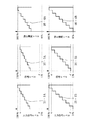
まず、図23は本実施例での最適化が行なわれる前の状態を示している。例えば、電源投入時や入力系統1と2(PC1入力とPC2入力)からの信号が伝送される直前である。まず、本画像表示装置の画像表示部として動作範囲が50Hzから85Hzの範囲にあり、かつ推奨される動作タイミングが75Hzの垂直周波数の表示部を接続したとすると、出力としてOVDは、まず75Hzに設定されている。また、この直後に、IVD1として、50Hzの垂直周波数の信号とIVD2として60Hzの垂直周波数の信号がそれぞれ入力されたときを示している。この状態では、まだ本回路で最適化は行なわれておらず、それぞれの周波数に応じてメモリが駆動されて、ダブルバッファによる表示が行なわれている。
【0144】
次に、図24は第一段階として入力系統2の60Hzを動画表示上優先すると判断した場合の動作を示している。この選択としては、例えば図21のマイコンに入力する同期信号IHD1、IHD2、IVD1、IVD2からマイコン部が2系統の入力信号の同期判別を行ない、解像度と垂直周波数を判定した結果を表3のように、マイコン部内に持つテーブルを参照して表3の(2)の動作を選択する。あるいは、図21の画像比較部10−3において、IVD2の系統がNTSCなどのTV系のインターレース信号をPC用にノンインターレース化した動画であり、IVD1の系統が静止画であるという判別を行なった場合も同様の決定がされる。図22のSW1、SW2−1、SW2−2はそれぞれIN2−2、IN4−1、IN5−2が選択される。これにより、図24の(e)に示すように、出力の垂直同期信号OVDはIVD2と同期が合わせ込まれる。これにより、IVD2の系の動画質は確保され、ダブルバッファリングの欠点であるフレームの二重化やフレームの抜けが発生しないスムーズな画面が実現される。また、IVD1の系は50Hzから60Hzに変換されるため表示部においてフリッカによる画質劣化を避けることができている。
【0145】
さらに、図25に第二段階として、IVD1の入力系統も動画の映像ソースを送出してきたことを図21の画像比較部10−3で検出して、マイコン部がIVD1の入力系の動画質を改善すべきと判断した場合や、システムの設定で常に動画質を各系統とも最善の状態に設定するようにマイコン部のソフトウエアが設計されている場合の例を示す。図21のマイコン部9はDDC1を介してIVD1の入力信号源に対して、垂直周波数を50Hzから60Hzに変更するよう要求し、IVD1の入力信号源は垂直周波数を60Hzに設定を変更する。これにより、IVD1はIVD2やOVDとは位相は一致していないが、周波数は一致するため、ダブルバッファリングをしていても、フレームの二重化やフレームの抜けが発生しないスムーズな画面が実現される。これにより、2系統とも動画質の最適化された表示装置が実現される。
【0146】
さらに、図26に第三段階として、画像表示部を変更した場合を示す。例えば、従来リア型のプロジェクションディスプレイを用いていたシステムをプラズマディスプレイに置き換えたり、古い型のディスプレイを新しい型に置き換えたりして、動作範囲が50Hzから85Hzまで可変できるタイプのディスプレイから、動作範囲が70Hzから100Hzのディスプレイに変更した場合が考えられる。
【0147】
このとき、図21のシステムのマイコン部はDDC3を介して新たに接続されたディスプレイの動作範囲から、60Hzでは動作しないものであることを検知して、出力系の動作周波数を70Hz以上に変更しようとする。また、マイコン部は、DDCや入力画質の情報から、特にIVD1の系よりもIVD2の系の動画質を優先させるべきと判断する。そこで、本実施例のマイコン部は、もとのIVD2の垂直周波数の周期(画面の更新周期)に近く、また周期の比が整数対整数の比になるような新しい垂直周波数の候補を出力可能な周波数の範囲から選択するとともに(例えば、75Hzを選択する。もとの60Hzとの周期の比はT(60Hz):T(75Hz)=5:4)、IVD2系のDDC通信を介してIVD2の系が60Hzの次に最適な周波数としてその垂直周波数で動作可能かを調べる。IVD2側が動作可能であれば、新しく選択された垂直周波数75HzにIVD2の系の動作周波数が設定されるとともに、画像表示部の垂直周波数も、IVD2の垂直同期信号に同期した75Hzに設定される。再び、図22のSW1、SW2−1、SW2−2はそれぞれIN2−2、IN4−1、IN5−2が選択される。これにより、図26に示すように、出力の垂直同期信号OVDはIVD2と同期が合わせ込まれる。また、これに伴ない、IVD1の系も動画質を良くするために、DDC1を介して75Hzに動作周波数を設定し直される。これにより、入力系、出力系ともに75Hzに動作を変更される。
【0148】
実施例の中で述べたように、60〜80Hzという周波数は、現行のPCやWS(ワークステーション)やDTV(デジタルテレビ)等、最も広く普及している周波数帯である一方、TVからの動画の映像ソースもNTSCが60Hzのため、この範囲に入ってくるので使用頻度が非常に高く、動画を最優先させる意味は高い。
【0149】
一方、50Hzなど、低い周波数のフリッカ現象は、動画、静止画に関らず非常に見づらい画質劣化となる点から、ダブルバッファリングのような簡易的に動画に強い方式をとる方法で、フリッカ防止と動画画質向上を両立させている。
【0150】
また、100Hzのように高い垂直周波数の信号に関しては、100MHzを超える動作速度が回路的な負担が大きいことを重視し、ダブルバッファリングのような簡易的に動画に強い方式をとる方法で、コスト削減と安定動作を動画画質向上と両立させている。特に液晶やPDPなどの表示素子は駆動電圧が10数Vから数十Vという高電圧が必要とされるため、1画素あたりの速度が高速化すると、映像信号系やドライバ回路が非常に高い帯域やスルーレートが必要とされる。現状においても、こうした高い速度の駆動に対しては追従できない部分を、複数に分割駆動しているが、更なる出力系の高速化は高速な部品への変更、新規部品の開発、分割数の変更などの回路変更によるコストアップばかりでなく、回路の動作マージンを狭くし、安定的な動作を困難にする要因となる。また、この問題はSXGAやUXGAといった、現状よりも更に数倍画素数の多い表示素子などを駆動する場合に、特に重要になる。将来の高画素化のためにも、コスト削減と安定動作が動画画質向上と両立できる点が重要になってくる。
【0151】
さらに、このような垂直周波数の最適化を図る際に、出力の垂直同期が完全に一致できるのは、複数の系統のうち一つしかないため、複数系統の入力画像のどれを優先して垂直同期を一致させて動画質を確保するかの選択を可能にしたことで、複数系統のなかで動画質を重視する入力系統が、アプリケーションソフトや番組などにより変化した場合も、安価でありながら、柔軟に対応できるシステムが構築できる。
【0152】
また、選択された出力同期周波数に対して、同期していない入力系統に対して、DDC等を介して入力信号源に対して入力周波数の変更を要求し、出力周波数と一致した周波数に変更することにより、複数画面の入力系とも動画質が最適に表示されるため、デジタルTVやPCのグラフィックゲームソフト、デジタルビデオ等、さまざまな動画ソースが表示されるマルチ画面の表示装置において、安価でありながら、動画質を十分満たせる機器を提供できる。
【0153】
また、画像表示部が異なるタイプのディスプレイに変わったことにより(例えばリア型のプロジェクションディスプレイからプラズマディスプレイなど)、対応可能な動作周波数の帯域が変化した場合も、DDCやその他の通信を介して得られる画像表示部の特性の情報を受けて、内部の出力周波数の選択範囲や選択方法を変更するのに加えて、DDCを介して複数の入力信号系に要求する内容も変更をかける構成にしたことで、安価でありながら、将来的なシステムの変更やシステムの拡張に対しても柔軟で、かつ動画質の最適な機器が実現できる。
【0154】
本実施例では、複数の入力に接続される機器からの通信手段として、DDC(DDC1、DDC2)を、また出力する画像表示装置との通信手段としてDDC(DDC3)を示しているが、これはVESAの標準(現在DDCver.3.0 1997.12.15発行)が、現在ディスプレイの情報をPCに通信する手段として最も普及しているため、例示してあるだけであり、USBやIEEE1394、従来のシリアル通信、パラレル通信手段など画像処理機器間で情報を通信できる手段であれば任意のものでよい。特にVESAの標準に関しては、逐次改定されているが、現在のところ、本発明のような複数のホスト機器(信号発生器やPC)と表示機器の接続は前提とされておらず、アドレス間の調停などの観念もない。また、通信時期もホスト(PC)側の起動時に限られているため、このままでは本発明に利用できない。本実施例では、通信手段の実現方法の例として、通信線の形態をDDCと同じI2Cの2線式シリアルバスを3系統DDC1,DDC2,DDC3用意して、データ形式(フォーマット)もDDCの用いている標準EDID(現在EDIDver.3.0 1997.11.13発行)などに準じた形式にしている。これにより、複数の入力機器はホストとして、本実施例の画像処理装置をディスプレイとして扱いDDC情報を通信する。また、本実施例の画像処理装置は、接続される表示装置には、自身がホストとして表示装置をディスプレイとして扱い、DDC情報を通信する。これらの複数の入力機器と表示装置のアドレス間の調停やホスト役の切替えは、本来のDDCでは規定されていないので、本実施例の図21のマイコン9が制御する。また、ホストの起動時のみではなく、機器の接続切替え時にも通信を行なえるような検出と制御も、DDCでは規定されていないので、本実施例の図21のマイコン9で対応する。このようにして、本発明を実現している。他の実施例においても同様である。
【0155】
ここでは、使用頻度の高い垂直周波数帯域を同期を一致させ、それ以外の周波数をダブルバッファリングさせたが、ダブルバッファリングは、メモリ領域を倍必要とすること、またそのための制御回路部分が必要となるため、入力系統数が多くなると高価になるため、機能として省くことも考えられる。特定の垂直周波数帯域のみ同期を一致させる方法やダブルブァッファする方法をとる一方で、その帯域以外の使用頻度は低いと判断し、動画質は改善しない単なる非同期な動作に切り換えることを行ない、複数の入力系のうち動画を優先する系統のみ選択切り替えて動画質を確保する方法も安価な製品を提供する意味で本実施例の一つの形態である。
【0156】
また、本実施例では、入力信号の垂直周波数により、出力系を入力系と同期させるか非同期とするかを選択したが、本実施形態は複数の入力系の動作モードや画質特性から最適な出力系の動作モードや画質特性を選択する回路を有すること、および表示部を含む出力系の動作モードや画質特性と複数の入力系の動作モードや画質特性から、システム全体の動作モードや画質特性を決定する回路を有すること、またその決定にしたがって任意の入力系の動作モードや画質特性の変更を要求する回路を有することが特徴であり、切り換える基準は入力信号の垂直周波数以外にも、入力信号のフォーマットの他の項目でや、入力画像から抽出した画像情報、入力画像の信号の内容、システムの動作モード、画面の表示割合や配置条件、ユーザー設定、省電力モードなどによる場合も含んでいる。
【0157】
また、切り替える対象として、本実施例は動画質に着目して垂直周波数を例示したが、他の画質特性に対しても、入力信号のフォーマットの他の項目、例えば解像度や画像の表示位置、画像の大きさ、色相、色度、ホワイトバランス、明るさ(ブライト)、明暗(コントラスト)、階調性(ガンマ特性)、ダイナミックレンジ等に関しても、同様である。
第4の実施例において、この例の一つとして階調性の例を示す。
【0158】
(実施例4)
第3の実施例と同じ図21を用いて、第4の実施例を示す。ここで、図21における各部の構成および動作は第3の実施例と同じである。
本実施例においては、10−3の画像比較部において、各入力系の画質の比較を行ない、マイコンが出力系と各入力系の画質制御を行なうための情報の出力を行なう。入力系画像処理部1および入力系画像処理部2から出力される画像信号から比較用に抽出された比較信号20−REF−1、20−REF−2から得られた比較情報の演算結果がマイコンバス19−1を経由してマイコンに伝達される。
【0159】
本実施例において、画像比較部から得られる各入力系の画質特性の比較結果に加えて、DDC3やほかの通信経路、初期情報等で与えられる表示部の特性や条件との比較を行ない、内部の各画像処理部(入力系画像処理部1、入力系画像処理部2、出力系画像処理部)を制御するとともに、DDC1、DDC2を介して入力信号源の画質制御を行なう。
【0160】
ここで、本実施例での画質の主要な調整部は出力系画像処理部6に存在し、入力画像処理部3−1、3−2の画質調整部は補助的に存在する。これは、画像のビット誤差の増大を避けるためであり、画質を優先する系は入力の画像処理部の画質調整部をバイパスする構成として、出力系の調整部のみにより、画像表示部に適した特性に変換される。また、もう一方の系は、補助的に入力画像処理部の画質調整も行ない、優先した系と同様の画質になるように調整される。あるいは、優先しない方の系は、入力画像処理部での画質調整を行なうかわりに、DDCを介して入力信号源に、入力信号の画質を変更する要求を出すことで、優先した系と同様の画質になるように調整される。
【0161】
これにより、複数の入力系の様々な画質特性の入力画像を1画面上に合成してマルチ画面表示を行なう際に、各入力系と出力表示部の画質特性に応じて、システム全体の画質が最適化される。
【0162】
図27から図29を用いて、本実施例の動作を説明する。
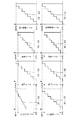
図27は、本実施例による画質の最適化が行なわれる第一段階の状態を示している。このとき、表示部の表示特性は図15の15−1である。図27において、16−1A、16−1Bは2系統の入力IDATA1およびIDATA2から入力する信号レベルを示し、16−3A、16−3Bは出力画像処理部6の通過後の各信号レベルをあらわす。また、16−4A、16−4Bはこのときの表示部の輝度レベルを示す。
【0163】
第一段階として、マイコン部は、入力系画像処理部1(3−1)と入力系画像処理部2(3−2)からの画質情報(20−REF−1、20−REF−2)を比較して得られた画像比較部(10−3)の結果と、DDC3経由や、あらかじめマイコン部付随のメモリ上に記憶されたテーブル等から得られる画像表示部の入出力特性から、画質を優先する入力系を決定する。ここでは、入力系2(IDATA2)を優先させると判断している。ここで、従来例と異なり、優先する系の入力信号の表示部に対する特性の変換は、入力系の画質処理部ではなく出力系の画質処理部で一括して行なわれる。変換係数は、あらかじめマイコン上で入力系2の特性と出力系の特性を合成して出力系画像処理部に適用することにより、デジタル処理の通過回数を半分にして、ビット誤差を少なくしている。また、このとき入力系1の画像に対しても同じ合成した変換係数が適用されるため、16−3Aのように、入力系1の画質の最適化は行なわれていない。
【0164】
次に、第2段階として、マイコン部は優先しない入力1の系に対しても、画質の最適化を行なった様子を図28に示す。図28において、16−1A、16−1Bは2系統の入力IDATA1およびIDATA2から入力する各信号レベルを示し、16−2A、16−2Bは入力画像処理部1(3−1)と入力系画像処理部2(3−2)の通過後の各信号レベルを示す。16−3A、16−3Bは出力画像処理部6の通過後の各信号レベルをあらわす。また、16−4A、16−4Bは、このときの表示部の輝度レベルを示す。
【0165】
第一段階で調整されたIDATA2の系(16−1B〜16−4B)に対して、第二段階ではIDATA1の系を調整する。このとき、出力画像処理部6の変換特性は入力2(IDATA2)で決定されているので、この特性に対する、入力1(IDATA1)の入力補正の差分を入力画像処理部1(3−1)に適用する。この結果、入力画像処理部1(3−1)通過後の信号レベル16−2Aは、入力画像処理部2(3−2)通過後の信号レベル16−2Bにほぼ等しくなり、出力画像処理部上では、16−3Bとほぼ同じ信号レベル16−3Aで出力され、また、16−4Bとほぼ同じ輝度レベル16−4Aで表示が行なわれる。
このように、優先しない系に対しては、ビット誤差は大きくなるものの、優先した系と同様の特性に調整を行なうことができる。
【0166】
さらに、第三段階として、図15の15−2の特性のものに画像表示部7を変更した場合を図29に示す。図29において、16−1A、16−1Bは2系統の入力IDATA1およびIDATA2から入力する各信号レベルを示し、16−3A、16−3Bは出力画像処理部6の通過後の各信号レベルをあらわす。また、16−4A、16−4Bは、このときの表示部の輝度レベルを示す。
【0167】
画像表示部の変更に伴ない、マイコン部は、DDC3経由や、あらかじめマイコン部付随のメモリ上に記憶されたテーブル等から得られる変更後の画像表示部の出力特性を読み込み直す。この情報と、各入力系の画質情報から画質を優先する入力系を再度決定する。
【0168】
ここでは、再び入力2(IDATA2)を優先すると判断したとする。変換係数は、マイコン上で入力系2の特性と新しい出力系の特性を合成して出力系画像処理部に適用され、16−3Bが出力される。この結果、画像表示部の表示特性に最適化が行なわれた輝度レベルが選られる(16−4B)。また、第三段階では、さらに、入力系1に対しても画質のビット誤差を少なくするため、第二段階のような入力系1に対しての入力信号処理部での変換を行なわず、DDC1を介して入力信号源1に対して、信号振幅とレベルを入力信号源2に一致させるように要求を出して、16−1Aのように入力系1の入力信号の特性を、16−1Bの入力系2の入力信号の特性に等しくなるようにする。入力信号の段階で二つの入力系の信号レベルを一致させることにより、両方の系ともデジタル処理の通過回数を半分にして、ビット誤差を少なくしている。
【0169】
以上に述べたように、画像比較部から得られる各入力系の画質特性の比較結果に加えて、DDCや他の通信経路、初期情報等で与えられる表示部の特性や条件との比較を行ない、内部の各画像処理部(入力系画像処理部1、入力系画像処理部2、出力系画像処理部)を制御するとともに、DDCなどの通信手段を介して入力信号源の画質制御を行なうことにより、複数の入力信号を一つの画面に表示するマルチ画面表示においても、安価で簡単な回路構成でありながら、優先する系の高画質表示を実現するとともに、他の系の画質も一定の水準を満たすシステムが実現できる。
【0170】
本実施例においては、簡単化のため、グレースケール信号を用いて、画質として信号のDCレベルと振幅の最適化を行なう例を述べたが、実際には、表示素子の特性を補正するガンマ補正や、CRT用に映像信号に掛けられているガンマ補正をキャンセルする逆ガンマ補正などの非線型な補正に対しても同様に適用できる。また、赤、青、緑毎にこれらの特性が異なることにより生じるホワイトバランスのずれ、色の特性についても、本実施例を適用することにより、優先する入力系を選択して、出力系の特性と合わせて、各色のバランスを合わせ込み、他の系は補助的な手段を用いて、あるいは入力信号源に制御信号を送ることにより一定の水準を満たすように調整してシステムの最適化を図ることができるのは同様である。色毎の特性がばらつく原因としては、赤、青、緑毎に異なる液晶パネルを用いる3板式のプロジェクタなどに見られるような各色ごとの液晶素子のガンマ特性のばらつきや、色を光学系で3原色に分解するための各光学素子の色毎の特性のばらつき、バックライトやLED、ランプなどの発光体の特性、各色ごとの信号処理系のばらつきなどがある。
【0171】
特に、信号処理系のばらつきは、各信号源やその信号源に信号データが送られてくる以前の処理系でも意外と大きいことがあり、これがその装置特有の色味になっていたりすることも少なくない。これは、ディスプレイとして、ある色を強くした方が、鮮やかにみえるというメーカーの故意の調整であったり、製造上での各色での信号処理系の調整工数を減らしてコスト削減を行なうため省略されたためのばらつきであったりする。
【0172】
さらに、こうした故意の調整や工数削減によるばらつきなどは色だけに限られることではない。特にPCのグラフィック画面やデジタルテレビ、通信を介して受信されたテレビ会議の映像、インターネットを経由してきた画像情報、テレビゲームのグラフィック画像、USBやIEEE1394を介して受信したデジタルビデオカメラの映像など信号源や伝送形態の種類の多様化に伴ない、機器間のこうした特性差は広がりつつある。また、解像度や画面のリフレッシュレートなどの表示動作の差も多様化している。一方、表示装置はこれらの多様な入力ソースを同じ画面で表示する方向に動いており、こうした意味で本実施形態の有効性も広がっている。
【0173】
第3および第4の実施例においては、複数の入力信号源としてPCを2系統接続した例を挙げたが、第5の実施例としてはこうした多様化した機器間での適用例を示している。
【0174】
(実施例5)
第5の実施例として多様化した機器間での適用例として、PC(パーソナルコンピュータ)上に画像処理の入出力基板を備えて、表示装置を表示させるシステムの例を図30に示す。入力としては、画像処理基板に直接他のPC等を接続する2系統のデジタル入力の他に、PC本体のCPUで実行されるアプリケーションにより描画されるグラフィック画像および、通信IFを介して受信されるTV会議などの画像情報、IEEE1394を介して入力されるDVDやデジタルビデオ、デジタルテレビ等の信号が扱える。また、出力信号は、画像処理基板に直接接続する表示装置の他に、IEEE1394を介して外部のデジタルテレビやビデオ記録用のサーバーなどに送ることができる。
【0175】
図30において、9−1はPCのCPU(中央演算処理部)であり、9−2はチップセットと呼ばれるCPU周辺のメモリや周辺機器の制御するバスを制御するメモリ・バスコントローラであり、9−3はPC本体のメインメモリである。9−4はPCの通信インターフェース部であり、端子1−tを介して、外部の通信線に接続される。19−2、19−3はこのPCのシステム制御用バスであり、19−4はグラフィック部の制御用のバスである。25の一点鎖線で囲んだ領域が画像処理基板であり、PC本体とは端子1−4を介して、グラフィック制御バス19−4に接続される。
【0176】
1−1aは1系統目の入力としてのqビットのデジタルの画像信号(IDATA1)の入力端子である。1−1bは入力信号の水平同期信号(IHD1)入力端子であり、1−1cは入力信号の垂直同期信号(IVD1)入力端子である。1−1dは画像信号のクロック(ICK1)入力端子であり、1−1eはDDC信号(DDC1)の入出力端子である。20−1a−1、20−1a−2は各部へnビットのデジタルの画像信号を伝送するデータバスである。また、20−1bcdはIHD1、IVD1、ICK1信号線群である。20−1eはDDC1の信号線である。
【0177】
1−2aは2系統目の入力としてのnビットのデジタル画像信号(IDATA2)の入力端子である。1−2bは入力信号の水平同期信号(IHD2)入力端子であり、1−2cは入力信号の垂直同期信号(IVD2)入力端子である。1−2dは画像信号のクロック(ICK2)入力端子であり、1−2eはDDC信号(DDC2)の入出力端子である。20−2a−1、20−2a−2は各部へnビットのデジタルの画像信号を伝送するデータバスである。また、20−2bcdはIHD2、IVD2、ICK2信号線群である。20−2eはDDC2の信号線である。
【0178】
3−1は入力系1の画像処理部Aであり、3−2は入力系2の画像処理部Bである。
【0179】
1−3は、3系統目の入力かつ外部出力として機能するIEEE1394の入出力端子である。23はIEEE1394の処理ブロックであり、24はIEEE1394信号を内部で扱う映像信号と同期信号に変換および逆変換するためのエンコーダ兼デコーダである。また、3−3は入力したIEEE1394画像の画像処理部Cであり、6−3はIEEE1394信号として出力する前の出力系の画像処理部Bである。
【0180】
20−3はIEEE1394の信号線であり、20−3a−1は変換後のrビットのデジタル画像信号である。また、20−3bcdは、IEEE1394信号から再生された同期信号、CLKなどの信号線群である。
【0181】
また、4系統目の入力として1−4の端子を介して、19−4のグラフィック制御用バスからPCのアプリケーションプログラムにより生成されるグラフィック情報と、外部機器から通信線を介してPCに入力される画像情報が入力される。9−6はこれらの情報からグラフィックデータを出力するグラフィック生成・制御部Dであり、20−4a−1がvビットのグラフィックデータの信号線群である。また、20−4bcdはこのグラフィック画像の同期信号とクロックの信号線群である。また、19−5は端子1−4を介して外部バス19−4に接続されるグラフィック制御用の内部バスであり、この画像処理ボードの全体の制御はこのバスを介して、PC本体のCPUとグラフィック生成・制御部が分担して行なう。
【0182】
4は3つの入力画像処理部3−1、3−2、3−3とグラフィック生成・制御部9−6のあわせて4系統から入力した画像信号を、一旦メモリに記憶し、マルチ画面として出力するために、画像を合成して、出力系の画像処理部に出力する制御を行なうメモリ制御部である。5−1、5−2、5−3、5−4は入力系1、入力系2、入力系3およびグラフィック生成部にそれぞれ対応したフレームメモリ(メモリA、メモリB、メモリC、メモリD)である。21−1、21−2、21−3、21−4はそれぞれメモリA、B、C、Dの制御バスであり、22−1、22−2、22−3、22−4はそれぞれメモリA、B、C、Dのデータバスである。
6−1は出力系の画像処理部Aであり、7は液晶やプラズマディスプレイ、CRTなどの画像表示部である。
【0183】
1−fは画像表示部のkビットのデジタルデータ(ODATA)の画像表示部の入力端子であり、1−gは出力信号の水平同期信号(OHD)の画像表示部の入力端子であり、1−hは出力信号の垂直同期信号(OVD)の画像表示部の入力端子である。1−iは出力画像信号のクロック(OCK)の画像表示部の入力端子である。20−f−1、20−f−2、20−f−3はkビットのデジタルの画像データ(ODATA)の信号線である。また、20−g−2、20−h−2、20−i−2は、外部表示装置への水平同期信号、垂直同期信号、クロックの各信号線である。また、1−sは、画像表示部に対するDDC信号(DDC3)の入出力端子であり、20−s−1、20−s−2は、このDDC3の信号線である。
【0184】
12は発振部であり、出力系のクロック(OCK)を発生する。20−i−1はOCKの信号線である。発振部12は水晶などの発振回路やPLL(Phase−Locked−Loop)回路などで構成される。
【0185】
10−4が内部および外部の同期制御部であり、20−WEはメモリA〜Dの書込みフィールドの制御信号群、20−REはメモリA〜Dの読み出しフィールド制御信号群である。20−ghiは出力系の水平同期信号、垂直同期信号、クロックの各信号線群である。また、20−CNT−6はIEEE1394信号処理ブロック23の同期信号とクロックを制御するための制御線である。
【0186】
また、10−5が画像比較部および内部、外部の画質制御部であり、20−CNT−1および20−CNT−2は入力系画像処理部AとBからの画像抽出情報のデータ線および、入力系画像処理部AとBの画質を制御するための制御線からなる信号線群である。20−CNT−3はIEEE1394信号処理ブロック23内の入力画像処理部Cと出力系画像処理部Bからの画像抽出情報のデータ線および、入力系画像処理部Cと出力系画像処理部Bの画質を制御するための制御線からなる信号線群である。20−CNT−4はグラフィック生成・制御部からの画像抽出情報のデータ線および、グラフィック生成・制御部の画質を制御するための制御線からなる信号線群である。20−CNT−5は出力系画像処理部Aからの画像抽出情報のデータ線および、出力系画像処理部Aの画質を制御するための制御線からなる信号線群である。
【0187】
さらに、9−5は内部・外部同期制御部(10−4)と内部・外部画質制御部(10−5)との連携をとり、入力信号のDDC信号DDC1およびDDC2と、画像表示部のDDC信号DDC3を送受信するためのDDC用のインターフェース部である。また、20−u−1、20−u−2は、それぞれ内部・外部同期制御部(10−4)および内部・外部画質制御部(10−5)とこのDDC用インターフェース部間のデータ線および制御線である。
【0188】
画像の入力端子1−1aから入力したデジタル画像信号は、5−1のメモリ部Aに格納される前に3−1の入力系画像処理部Aで画質の調整や画像の縮小変換等の処理を行なわれてから、4のメモリ制御部に転送される。また、入力系画像処理部Aから画質を比較するための信号が、画像比較部に送出される。また、同期信号およびクロックは内部・外部同期制御部10−4に伝送される。
【0189】
画像の入力端子1−2aから入力したデジタル画像信号は、5−2のメモリ部Bに格納される前に3−2の入力系画像処理部Bで画質の調整や画像の縮小変換等の処理を行なわれてから、4のメモリ制御部に転送される。また、入力系画像処理部Bから画質を比較するための信号が、画像比較部に送出される。また、同期信号およびクロックは内部・外部同期制御部10−4に伝送される。
【0190】
IEEE1394入出力端子1−3から入力したIEEE1394信号は、内部で扱える画像信号と同期信号に変換される。5−3のメモリ部Cに格納される前に3−3の入力系画像処理部Cで画質の調整や画像の縮小変換等の処理を行なわれてから、4のメモリ制御部に転送される。また、入力系画像処理部Cから画質を比較するための信号が、画像比較部に送出される。
さらに、IEEE1394として外部出力する場合は、この出力画像処理部Bでの画像情報も画像比較部に送出される。また、同期信号およびクロックは内部・外部同期制御部10−4に伝送される。
【0191】
また、グラフィック生成・制御部9−6では、アプリケーションソフトやグラフィックドライバーソフトの指示に従って、内部・外部同期制御部(10−4)で作成した同期信号とクロックが入力するとともに、グラフィック信号を生成して5−4のメモリ部Dに格納されるために4のメモリ制御部に転送される。このとき、画質の制御は内部・外部画質制御部(10−5)によって行なわれる。
【0192】
メモリ制御部では、内部・外部同期制御部(10−4)で作成した出力系の同期信号とクロックにしたがって各メモリA〜Dより信号が読み出され、合成される。このとき、出力系画像処理部Aでの画像情報も画像比較部(10−5)に送出される。
本実施例では、このメモリ部A〜Dのいずれもダブルバッファリング可能なメモリ領域を確保し、同期制御部のメモリ書き込み信号と読み出し信号の制御線群(20−WE、20−RE)で書き込みと読み出すメモリ領域を切替え制御する。
【0193】
さらに、内部・外部同期制御部からの出力系のクロックOCKと水平同期信号OHD、垂直同期信号OVDに同期して所定の画像の大きさ、表示位置の関係にあったタイミングで4系統の画像データをメモリ部から読み出して、6−1の出力系画像部にデータを転送する。
6−1の画像処理部では、画質の調整や、画像の拡大変換などが行なわれる。最後に画像表示部7にこれらの画像データと同期信号、クロックが伝送され画像表示が行なわれる。
【0194】
本実施例においても、10−4の内部・外部同期制御部において、実施例3同様、動画像を優先する入力系を選択して、システム全体の動作の最適化を行なうことができる。ここには入力系1、入力系2、入力系3の同期信号とクロックが入力する。また、DDCインターフェース部を介して、画像表示部と入力系1および入力系2のDDCが接続されている。また、内部バス19−5を介してグラフィック作成・制御部が実行するアプリケーションソフトや通信からの画像表示の動作の要求内容が入力される。さらに、10−5の画質比較部により入力系1〜3の画像抽出情報で画像の特性情報が得られる。これらの情報から、内部・外部同期制御部は入力4系統の動作タイミングと画像の動画質特性および、画像表示部の動作特性を判断して、優先させるべき入力系の動画像に適した出力系動作となるように、メモリの制御信号と出力系の同期信号とクロックを作成する。また、グラフィック作成・制御部の同期信号およびクロックには、出力と同期したタイミングの信号を送出する。さらに、それ以外の入力系に対しても、動作の最適化を行なう必要がある場合は、入力系1および2に対してはDDCなどの通信手段を介して、入力信号源の動作を変更する要求を行なう。また入力系3の場合は制御線20−CNT−6を通じてエンコーダ・デコーダ部24で要求信号をIEEE1394信号に変換して、さらにこの信号がIEEE1394を通じて信号源の装置の制御を行なうことにより、入力信号源の動作を変更する。
【0195】
また、本実施例においても、10−5の内部・外部画質制御部において、実施例4同様、画質を優先する入力系を選択して、システム全体の画質の最適化を行なうことができる。ここには入力系画像処理部A〜Cから抽出された画像情報が入力するとともに、グラフィック生成・制御部から抽出された画像情報も入力される。また、出力系画像処理部Aからの画像抽出情報と、画像表示部7からDDCインターフェースを介して得られる表示特性が入力される。また、出力系画像処理部Bからの画像抽出情報と、IEEE1394を介して得られるIEEE1394で接続された別の表示装置の表示特性も入力される。これらの情報から、内部・外部画質制御部は入力4系統の画質特性および、画像表示部7の画質表示特性とIEEE1394経由で接続される別の表示装置の画質表示特性を判断して、優先させるべき入力系に適した画質特性となるように、出力系画像処理部Aもしくは出力系画像処理部Bを制御する。さらに、それ以外の入力系に対しても、画質の最適化を行なう必要がある場合は、各入力系の画像処理部により画質の調整を行なう。あるいは、入力系1および2に対してはDDCなどの通信手段を介して、入力信号源に対して画質を変更する要求を行なう。また入力系3の場合は制御線20−CNT−6を通じてエンコーダ・デコーダ部24で要求信号をIEEE1394信号に変換して、さらにこの信号がIEEE1394を通じて信号源の装置の制御を行なうことにより、入力信号源からの信号の画質を変更する。
【0196】
本実施例において、優先する入力系を選択して、最適化を行なうシステム全体の最適化の判断は、10−4の内部・外部同期制御部や、10−5の内部・外部画質制御部のブロックでハード的に処理される場合以外に、9−6のグラフィック生成・制御部あるいは9−1のCPUにおいて、アプリケーションソフトあるいはグラフィック制御用のドライバーソフト等によりソフト的に実行される場合もあることはいうまでもない。
【0197】
これにより、複数の入力系の様々なフォーマットと画質特性の入力画像を1画面上に合成してマルチ画面表示を行なう際に、各入力系と出力表示部の画質や動画の特性に応じて、システム全体の動作タイミングと画質が最適化される。
【0198】
ここでは、各入力系毎の整合性を考えたが、実際には各信号源からの信号は一種類の信号源からの出力のみとは限らない。例えば、IEEE1394にはDVDとデジタルビデオ、衛星放送やケーブルテレビ、地上波放送等のセットトップボックスなどの複数の機器が接続される。本実施例は、こうした1入力において混合された複数の画像情報も各入力信号源の一つ一つと考えて適用可能であり、IEEE1394端子等から入力するこうした複数の機器からの信号と、他の入力系の信号とを同列にならべた上で、優先する信号を選択して、動画質および画質特性のシステム全体の最適化を行なうことができる。
【0199】
また、優先する入力画像の選択は、画像抽出情報や画像信号のフォーマットだけではなく、入力する画像の用途や種類および自動設定あるいはユーザー設定される表示画面上の各画像の配置条件によっても行なわれる。例えば、本実施例において図31および、表4のように各入力映像信号が合成表示される画面を考える。
【0200】
【表4】
表4において、各列は各信号入力源の信号の用途や種類を示す。ここでは、例として▲1▼IEEE1394を介してデジタルTV信号と、また、▲2▼通信IFを介してTV電話と、さらに▲3▼外部PC入力からインターネットの画像が入力してきた場合を挙げている。また、表4の行には、用途により自動設定されたり、その表示装置を見ているユーザーが用途に応じて最も注目する画面として、例えば最前面に配置するなどの配置条件により選択された画像が示されている。表4の(a)〜(d)が図31の(a)〜(d)に対応している。そして、○印が、その入力源の信号の用途や種類と配置条件において、本実施例の回路が優先して選択する入力信号源である。
【0202】
図31および表4において、まず、(a)の表示画面では、最前面にデジタルテレビ画面が配置されている。このとき、画像表示部には、他にインターネット画面は子画面で表示されているが、それは最も注目される表示物ではなく、また静止画が主体である。また、TV電話の画像も入力しているが、現在は受信していない状態である。したがって、同期制御部および画質制御部は優先する入力系としてデジタルテレビの信号を選択して、システム動作を最適化する。
【0203】
また、(b)の表示画面では、最前面にTV電話の画面が配置されている。このとき、画像表示部には、他にインターネット画面は子画面で表示されているが、それは最も注目される表示物ではなく、また静止画が主体である。また、デジタルテレビ画面の画像も入力しているが、現在は小さく表示されている状態である。したがって、同期制御部および画質制御部は優先する入力系としてTV電話の画面の信号を選択して、システム動作を最適化する。
【0204】
また、(c)の表示画面では、最前面にインターネット画面が配置されている。このとき、画像表示部には、他にデジタルテレビの画像が子画面で表示されている。また、TV電話の画像も入力しているが、現在は小さく表示されている状態である。ここで、同期制御部および画質制御部は優先する入力系として、デジタルテレビの画像の信号を選択して、システム動作を最適化する。これは、配置条件としてはインターネット画面が最前面であるが内容が静止画主体のため、デジタルテレビを最優先する入力と判断したためである。
【0205】
一方、(d)の表示画面でも、最前面にインターネット画面が配置されており、画像表示部には、他にデジタルテレビの画像と、TV電話の画像も入力している。(c)と比較して違う点は、インターネット画面上で配信される動画情報の映像が小さなウインドウ▲4▼で表示されている点である。ここで、同期制御部および画質制御部は優先する入力系として、インターネット画面の信号を選択して、システム動作を最適化する。これは、配置条件としてはインターネット画面が最前面であり、また内容が動画主体になったため、デジタルテレビよりもインターネット画面が最優先する入力と判断したためである。
【0206】
このようにして、ユーザーが見る主体を変化させた配置条件やその信号の内容により、信号源の優先したシステム動作の最適化を図る。また、ユーザーは図30のシステムメモリ部に、これらの入力信号と配置条件における設定状態を保存できるようになっており、これによりユーザーの各種の映像機器と画像表示部の最適化関係を本実施形態の画像処理装置に記憶することができる。
【0207】
【発明の効果】
以上説明したように、本発明によれば、出力系を入力系の垂直同期信号に対して同期、非同期にすることを切換可能として、垂直周波数などの入力信号のフォーマットによって選択することにより、システムの全体を動画に強い構成として、特に使用頻度の高い垂直周波数帯で動画の問題のない動作を実現し、また、その他の垂直周波数帯では簡易的に動画に強くかつ画質上の問題の解決と動作マージンを確保し安定な動作を行なうことを両立する画像処理装置を簡素で安価に実現することができる。また、将来的にもUXGA等、現状よりも更に数倍画素数の多い信号処理用途で、容易に同様の構成で安価で動画に強い回路を実現できる。また、複数の異なる周期の入力信号が混在するシステムにおいても、複数の入力系の垂直同期信号に対して出力系を同期、非同期にすることを切換可能として、また、その結果を用いて任意の入力信号源の垂直周波数の設定を行なえるように構成することにより、出力系の構成は1系統のクロックで動作させながら、複数の入力系統間と出力の同期関係を最適化して、システム全体を動画に強い構成でかつ簡単で安価な回路構成にすることができる。
【図面の簡単な説明】
【図1】本発明の第1の実施例に係る画像処理装置のブロック図である。
【図2】図1の装置における同期制御部の構成図である。
【図3】図1の装置の動作を説明するためのタイミングチャートである。
【図4】本発明の第2の実施例に係る画像処理装置のブロック図である。
【図5】図4の装置における画像表示例である。
【図6】従来例を説明するための、画像処理装置のブロック図である。
【図7】図6の従来例における画像処理装置の動作を示したタイミングチャートである。
【図8】図6の従来例における動画での問題点の説明図である。
【図9】ダブルバッファリングを行なう時のメモリ領域を示す図である。
【図10】ダブルバッファリングにおける画像処理装置の動作を示したタイミングチャートである。
【図11】ダブルバッファリングにおける動画での問題点の説明図である。
【図12】ダブルバッファリングにおける動画での問題点の説明図である。
【図13】第2の従来例を説明するための、画像処理装置のブロック図である。
【図14】第2の従来例における画質の階調性に関わる問題点を説明するための図である。
【図15】第2の従来例における画質の階調性に関わる問題点を説明するための図である。
【図16】第2の従来例における画質の階調性に関わる問題点を説明するための図である。
【図17】第2の従来例における画質の階調性に関わる問題点を説明するための図である。
【図18】第2の従来例における画質の階調性に関わる問題点を説明するための図である。
【図19】第2の従来例における画質の階調性に関わる問題点を説明するための図である。
【図20】第2の従来例における階調性のビット誤差を説明するための概念図である。
【図21】本発明の第3および第4の実施例に係る画像処理装置のブロック図である。
【図22】図20の装置における同期制御部の構成図である。
【図23】本発明の第3の実施例の動作を説明するためのタイミングチャートである。
【図24】本発明の第3の実施例の動作を説明するためのタイミングチャートである。
【図25】本発明の第3の実施例の動作を説明するためのタイミングチャートである。
【図26】本発明の第3の実施例の動作を説明するためのタイミングチャートである。
【図27】本発明の第4の実施例の画質の階調性に対する動作を説明するための図である。
【図28】本発明の第4の実施例の画質の階調性に対する動作を説明するための図である。
【図29】本発明の第4の実施例の画質の階調性に対する動作を説明するための図である。
【図30】本発明の第5の実施例としての画像処理装置のブロック図である。
【図31】本発明の第5の実施例の動作を説明するための概念図である。
【符号の説明】
3,3−1,3−2:入力系画像処理部、4:メモリ制御部、5:メモリ部、6:出力系画像処理部、7:画像表示部、8:PLL、9:マイコン、10:同期制御部、12:発振器(第2クロック発生部)、ICK,ICK1,ICK2:入力系クロック(第1のクロック)、IHD,IHD1,IHD2:入力系水平同期信号(第1の画像同期信号)、IVD,IVD1,IVD2:入力系垂直同期信号(第1の画像同期信号)、OCK:出力系クロック(第2のクロック)、OHD:出力系水平同期信号(第2の画像同期信号)、OVD:出力系垂直同期信号(第2の画像同期信号)、RE:読み出しフィールド制御信号、WE:書込みフィールド制御信号。[0001]
TECHNICAL FIELD OF THE INVENTION
The present invention relates to an image processing apparatus that converts image signals having various formats into image signals of a desired format and combines the image signals.
[0002]
[Prior art]
With the recent increase in multimedia, the chances of displaying various image signal formats are increasing. In particular, in the past, TV sets and personal computer (PC) displays were completely different things. However, mutual fusion has progressed, and TVs that can display PC images and PC displays that can input TV signals have appeared. Have been. In addition, the appearance of video sources in new digital formats such as digital television and MPEG and the advancement of three-dimensional graphics have been progressing, and even in the case of PC displays, the rate of displaying moving images has been increasing.
[0003]
FIG. 6 shows a block diagram of such a conventional display. In the figure, 1-1 is an input terminal for an analog image signal, 1-2 is a horizontal synchronizing signal (IHD) input terminal for an input signal, and 1-3 is a vertical synchronizing signal (IVD) input for an input signal. Terminal.
[0004]
[0005]
Before the digital image signal is stored in the
[0006]
In recent years, large-screen display devices such as wide-screen TVs, plasma displays, rear projection TVs and projection projectors have been used for various displays such as movies, TVs, home videos, presentations, TV conferences, and various materials. The use of video sources in offices and homes is increasing. Further, in such a form, there is a multi-screen display device in which images of a plurality of different input sources are divided and displayed in one screen.
[0007]
FIG. 13 shows an example of a display conventionally used in such a scene. One of the displays has a digital computer image signal input, and the other has two PC inputs which are analog computer image signal inputs. FIG. 2 is a block diagram of an image processing unit of an image display device that performs output image synthesis by controlling output of a memory and performs two-screen multi-screen display on one system image display unit.
[0008]
In FIG. 13, reference numeral 1-1a denotes an input terminal of a q-bit digital computer image signal (IDATA1) of the first system (PC1). Here, there should be originally three systems of red, blue, and green (RGB), but for simplification of the configuration, only one system is shown (the same applies hereinafter). 1-1b is a horizontal synchronization signal (IHD1) input terminal of the input signal, and 1-1c is a vertical synchronization signal (IVD1) input terminal of the input signal. 1-1d is a clock (ICK1) input terminal of an image signal, and 1-1e is a DDC (DDC1) input / output terminal. 20-1a-1 and 20-1a-2 are data buses for transmitting q-bit digital image signals to each unit. 20-1b, 20-1c, 20-1d, and 20-1e are signal lines of IHD1, IVD1, ICK1, and DDC1, respectively.
DDC is a standard of communication means for a computer to recognize and control a display device, which is recommended by a standardization organization, VESA (Video Electronic Standard Association).
[0009]
1-2a is an input terminal for a second system (PC2) analog computer image signal (IDATA2). 1-2b is a horizontal synchronizing signal (IHD2) input terminal of the input signal, and 1-2c is a vertical synchronizing signal (IVD2) input terminal of the input signal. 1-2e is a DDC (DDC2) input / output terminal.
[0010]
20-2a-0 is an analog signal line, and 20-2a-1 and 20-2a-2 are n-bit digital signal lines. 20-2b, 20-2c, 20-2d, and 20-2e are signal lines of IHD2, IVD2, ICK2, and DDC2, respectively.
[0011]
Reference numeral 3-1 denotes an input image processing unit of the PC1, and reference numeral 3-2 denotes an input image processing unit of the PC2.
[0012]
An
An H /
[0013]
1-f is an input terminal of an image display unit for image display digital data (ODATA), 1-g is an input terminal of an image display unit for a horizontal synchronization signal (OHD) of an output signal, and 1-h is an output terminal. This is an input terminal of the image display unit for the vertical synchronization signal (OVD) of the signal. 1-i is an input terminal of an image display unit of a clock (OCK) of an output image signal, and 1-j is an input terminal of an image display unit of a microcomputer bus (MB).
[0014]
20-f-1, 20-f-2, and 20-f-3 are k-bit ODATA signal lines. 20-g-1 and 20-g-2 are OHD signal lines. 20-h-1 and 20-h-2 are OVD signal lines. 20-i-1 and 20-i-2 are OCK signal lines.
[0015]
The digital image signal input from the image input terminal 1-1a is processed by the 3-1 input system
The analog image signal input from the image input terminal 1-2a is converted into digital data by the
[0016]
The
[0017]
7, when the resolution of the
[0018]
In FIG. 7,
[0019]
[0020]
[0021]
Thus, the input system horizontal synchronization signal, vertical synchronization signal, and input clock have different periods depending on the resolution. In the apparatus shown in FIG. 6, the
[0022]
In the device shown in FIG. 13, in the case of the input system 1 (PC1 input), the input signal processing system is operated in synchronization with IHD1, IVD1, and ICK1 and recorded in the memory A. In the case of the input system 2 (PC1 input), first, the
[0023]
On the other hand, the output system is asynchronous with the signal of the input system, and generates OHD and OVD with a constant counter value from the output clock OCK by the counter circuit, and synchronizes the OCK, OHD, and OVD from the memories A and B with the OCK, OHD, and OVD. The two systems of images are read, synthesized, and sent to the output system image processing unit and image display unit. In this way, the resolution conversion and the vertical frequency, that is, the screen update frequency (frame rate) of the input system and the output system are converted.
[0024]
[Problems to be solved by the invention]
However, in the frame rate conversion, there is a problem of deterioration of the image quality of a moving image as shown in a specific example in FIG. Also in the description of FIG. 8, the same phenomenon occurs in FIG. 13 because the PC1 input system and the PC2 input system operate in the same manner. Here, the case where the ratio of the input vertical frequency to the output vertical frequency is 5: 4 (for example, 100 Hz and 80 Hz) is shown as an example. In FIG. 8,
[0025]
Since one screen is read while writing one screen in the same memory area, when the timing of rewriting one screen happens to be close to the timing of reading as shown in (a) and (f) and (e) and (i), there is no change on the screen. Although it does not appear, when the screen is rewritten while the screen is being read as shown in (g) and (h), the previous and next screens are switched in the middle of one screen, and the moving image is shifted up and down the screen. I can see it. This is called “image overtaking”, and is a phenomenon in which the quality of an image when displaying a moving image is degraded. Conversely, the same phenomenon occurs when the output vertical frequency is faster than the input vertical frequency.
[0026]
This phenomenon is more noticeable when a relatively large geometric object moves horizontally parallel to the screen, but it is less noticeable in natural images, etc. Conventional PCs use word processors, spreadsheets, drawing Because there are many uses of still images such as this, it did not become a big problem. However, as described above, even in the case of a PC, the opportunity to display a moving image has increased recently, and the number of screens on which a geometric graphic moves has also increased.
[0027]
As a measure against such a problem, there is a method called double buffering. This is because the memory area is prepared not for one screen but for two screens and the memory area is alternately switched every other screen for writing, and the reading is always performed for the memory area being read so as not to overtake the screen. This is a method of controlling so as to select a memory area so that the scanning has a relationship preceding the scanning scan of writing of the memory area.
[0028]
For example, when storing data of the number of pixels of XGA (1024 × 768), as shown in the memory map of FIG. 9, even numbers such as m, m + 2, m + 4... Fields are stored in the first memory area of addresses 00000h to BFFFFh. , And input images of odd-numbered fields such as m + 1, m + 3, m + 5... Fields are stored in the second memory area of C0000h to 17FFFFh. FIG. 10 shows a timing chart of the write and read operations of the memory at this time. 61 shows an input vertical synchronizing signal (IVD), and 64 shows an output vertical synchronizing signal (OVD). Since the description here is also common to the PC1 input and the PC2 input with respect to FIG. 13, the IVD indicates IVD1 or IVD2 (or both), and the first memory area and the second memory area are the memory A or the memory B ( Or both).
[0029]
Each time the
[0030]
As described above, writing is alternately written to the first and second memory areas at even and odd numbers of the input field, but reading is performed by selecting a field in which writing is not displayed. Here, since the output side has a higher vertical frequency with respect to the input, if the input field is writing the first memory area when the output VD becomes High, the second memory area is read and the second memory area is read. Is written, the first memory area is controlled to be read so that the overtaking phenomenon does not appear. When the vertical frequency on the output side is low, it is necessary to control so as not to overtake while checking the relationship between the input VD (IVD) and the output VD (OVD). In any case, the read timing of the first memory and the second memory is determined by scanning the memory area that is always being read in accordance with the input and output frequencies and the relationship between the synchronization signals. The setting is made so that the memory area is switched so as to have a relationship preceding the scanning.
[0031]
However, this double buffering method also has problems with moving images as described below.
In the case of double buffering, the other memory area is selected so as not to display the memory area currently being written, so that, for example, as shown in FIG. In the case where there is a screen of continuous motion such as rotating one hand, the same image as in (e) and (f) of the frame rate-converted output as in (e) to (i) of FIG. When there are screens such as “duplexing of frames” for two consecutive fields or input screens 81 (a) to (d) as shown in FIG. 12, the frame rate is changed to 82 (e) to (g). As shown in (c) of the output obtained by converting the "?", "Missing frame" in which the corresponding field is lost occurs.
[0032]
As a method of improving the moving image quality by a method different from the double buffering, there is a method of synchronizing the input vertical frequency and the output vertical frequency. In the case of a display unit of XGA (1024 × 768 pixels), when a 50 Hz input signal such as VGA (640 × 480) or SVGA (800 × 600) is input, the display is converted to XGA 50 Hz and displayed. Is a method of converting the input signal to XGA 100 Hz for display.
[0033]
In such a case, the problem of motion does not occur because the writing and reading cycles of the memory coincide. However, when the input signal source has a low frequency such as 50 Hz, a device such as a liquid crystal display in which the polarity is inverted for each field is half the frequency when viewed at the same polarity. There is a problem in image quality that the rewriting cycle of the data becomes slow and a flicker phenomenon that the entire surface flickers appears. In addition, when the frequency is as fast as 100 Hz, when the number of pixels is low such as VGA, the speed is about 2.6 times as fast as the input when converted into an output with the number of pixels of XGA even if the speed is not great. Therefore, there is a problem that the operation speed of the entire output system must be increased. For example, a clock rate of about 65 MHz at XGA of 60 Hz is about 108 MHz at XGA of 100 Hz, which exceeds 100 MHz. In order to solve this problem, it is necessary to adopt parts with a high operating speed, develop new parts, and divide the operating system to reduce the speed and adopt a circuit configuration.This has led to an increase in cost and an increase in circuit size. Would.
[0034]
In addition to the above problem, there is also a problem due to the fact that there are two or more inputs. As shown in the example of FIG. 13, since the input system operates in synchronization with each input signal, the PC1 input and the PC2 input are basically asynchronous, while the output system has two systems at the same timing. A method of synchronizing the vertical frequency of input and output for synthesizing and outputting an image on one screen can be implemented for either one system, but cannot be applied to two systems at the same time. This problem becomes a serious problem for a multi-screen application in which the number of input systems is increased and the image quality of each moving image is emphasized.
[0035]
Furthermore, for a plurality of image inputs, similarly to the image quality of a moving image, it is possible to optimize only one input system unique to a multi-screen in terms of various image quality characteristics such as color, brightness, contrast, etc. Alternatively, when optimizing, there is a problem that the circuit scale increases.
[0036]
Here, an example of a problem relating to image quality gradation, such as image contrast, brightness, and gamma characteristics, is shown in the circuit of FIG.
FIG. 14 shows a gray scale signal in which the gray scale changes in eight steps in the horizontal direction as one of the video signals input to the image processing apparatus shown in FIG. 14-1 is a display screen in gray scale, and 14-2 is a signal at this time. In 14-2, the horizontal axis is the time of one horizontal scanning period, and the vertical axis is the signal level. 14-3 is the horizontal synchronizing signal of the input signal at this time. Here, 0% to 100% are equally divided into eight levels in one horizontal period.
[0037]
FIG. 15 shows a luminance characteristic of a display screen with respect to an input signal in the
[0038]
Here, it is assumed that input signals having different signal levels, such as 16-1A and 16-1B shown in FIG. 16, are input to the two input systems IDATA1 and IDATA2 of PC1 and PC2 in FIG.
FIG. 16 shows display luminance levels 16-4A and 16-4B of two signals when the image display unit having the characteristics indicated by 15-1 in FIG. 15 is used. As shown in 16-4A and 16-4B, even if the input signals of the same number of gradations, 16-4B of IDATA2 has 100% white and 0% black, but the luminance level is almost 0% to 100%. On the other hand, the other 16-4A has an image in which black is shifted to the white side by about 60% and floats white. Therefore, when two screens are simultaneously displayed on the same display device, two screens having different black levels and different contrasts are mixed, resulting in a screen display that is very difficult to see.
[0039]
Here, when the input-system image processing unit 1 (3-1) and the input-system image processing unit 2 (3-2) in FIG. 13 have an AGC (Auto-Gain-Control) circuit, the DC of the input signal is reduced. Correction is performed on signals having different levels and amplitudes. However, when the image display unit is replaced with a display unit having the characteristics of 15-2 in FIG. 15, no signal correction is performed for the change in the characteristics.
[0040]
FIGS. 17 and 18 show input signals and luminance levels when the characteristics of the display unit are 15-1 and 15-2 in FIG. 17 and 18, input signals 16-1A and 16-1B to be input to two systems of input IDATA1 and IDATA2, an input image processing unit 1 (3-1), and an input image processing unit 2 (3-2) 3) shows the signal levels 16-2A and 16-2B after passing through the AGC circuit and the luminance levels 16-4A and 16-4B of the display unit when this signal is input. As shown in 16-4A and 16-4B in FIG. 17, in the input / output characteristic of 15-1, the gray scale is from 0% to 100% by AGC.
However, as shown in 16-4A and 16-4B in FIG. 18, the gradation is only from 0% to 60% in the input / output characteristics of 15-2, and several white side steps become a white-out image. I will.
[0041]
For such exchange of the characteristics of the image display unit, it is conceivable to provide the output system
[0042]
As described above, the input image processing unit of each signal has the correction characteristics of the input signal, and the output image processing unit has the correction characteristics of the display unit. Multi-screen display with less influence of variation is realized. The correction characteristics include brightness (brightness), light and darkness (contrast), gamma characteristics, and white balance resulting from a difference between these color systems.
[0043]
However, providing the correction characteristics of the image signal in both the input system and the output system as described above requires preparing a plurality of similar circuits, increasing the circuit scale, the number of adjustment items, and increasing the cost. . This is a problem particularly in a configuration having a large number of inputs.
Further, such a configuration causes deterioration of an image by passing through a digital processing system for characteristic correction two or more times. FIG. 20 shows a conceptual diagram for this explanation. 20, the x-axis indicates the level of the input signal, and the y-axis indicates the input level of the output signal. In this figure, in the 8-bit 256-stage digital processing system, (1) y = x input / output characteristics, (2) y = x 2 Table of
[0044]
When this is applied to the conventional example, it is equivalent to giving a characteristic conversion such as (2) in the input system and giving a characteristic conversion such as (3) in the output system. , The gray level of the black level is deteriorated, and the image quality is deteriorated like a false contour in the image.
In order to avoid this phenomenon, there is a method of increasing the number of operation bits, but this increases the cost and the scale of the processing system.
[0045]
As described above, conventionally, in a multi-screen display in which images of a plurality of input signal sources are displayed on the same display unit, a configuration for converting characteristics of different input images into the same display characteristics in response to a change in the characteristics of the display unit is of a scale. And the cost increases. In addition, the circuit configuration has a large bit error, and has a problem of deteriorating image quality. Therefore, the brightness, contrast, gradation, color, and the like of each input system cannot be easily adjusted.
[0046]
When the input image processing apparatus is provided with an AGC circuit, the dynamic range of the signal can be secured. However, since the signal is automatically corrected, the signal level to be originally displayed is also corrected. There was also the problem of ignoring.
[0047]
Of the present invention Eye It is an object of the present invention to realize an image processing apparatus in which the quality of a moving image is improved with a simple and inexpensive circuit configuration. Another object of the present invention is to realize an image processing apparatus that can flexibly perform processing suitable for moving image quality even for a plurality of input signal sources.
[0050]
Means and action for solving the problem
the above of The present invention to achieve the object Pertain to First Image processing device Performs an operation of an input system for writing image data to the memory unit in accordance with a first clock and a first image synchronization signal, with a memory unit having a storage area for storing an image of at least one screen, A clock control unit for performing an operation of an output system for outputting image data read from the memory unit in response to a second clock and a second image synchronization signal; a clock generation unit for generating the second clock; An image processing apparatus comprising: a synchronization control unit that inputs a clock and outputs the second image synchronization signal, wherein the synchronization control unit divides the frequency of the second clock and is asynchronous with the first image synchronization signal. A fourth image synchronization signal created by synchronizing the first image synchronization signal with the third image synchronization signal and the second clock is created, and the third image synchronization signal and the fourth image synchronization signal are created. Picture By switching the synchronization signal, and outputs as said second image synchronizing signal. Switching between the third image synchronization signal and the fourth image synchronization signal is performed by: Out The selection is made according to the purpose of use of the image to be input.
[0051]
The present invention Duplicate The present invention is also applicable to a case where a plurality of input-system signal processing units are provided, and image signals input thereto are appropriately combined and displayed. A second image processing apparatus according to the present invention , As a fourth image synchronization signal synchronized with the first image synchronization signal , A plurality of fourth image synchronization signals synchronized with each of the plurality of first image synchronization signals are created, and the created plurality of fourth image synchronization signals and the third image are asynchronous with the first image synchronization signal. One image synchronization signal is selected from the synchronization signals and output as the second image synchronization signal. No. The image synchronization signal serving as the
[0052]
The present invention Is , CRT and other transmissive and reflective display devices, liquid crystal display devices, image display devices such as PDPs (plasma displays) and charge emission display devices, CCD and CMOS type two-dimensional imaging devices, and video signal capture boards The present invention can be applied to any image processing apparatus that involves digital image processing.
[0057]
【Example】
Hereinafter, embodiments of the present invention will be described with reference to the drawings.
(Example 1)
FIG. 1 is a block diagram for explaining the first embodiment of the present invention. In the figure, 1-1 is an input terminal for an analog image signal, 1-2 is a horizontal synchronizing signal (IHD) input terminal for an input signal, and 1-3 is a vertical synchronizing signal (IVD) input for an input signal. Terminal.
[0058]
[0059]
Before the digital image signal is stored in the
[0060]
In FIG. 1,
[0061]
FIG. 2 shows a circuit configuration example of the
In FIG. 2,
[0062]
925, 926 and 927 are clock input terminals of each counter, 930, 931 and 932 are clock enable terminals of each counter, and 934, 935 and 936 are output terminals of each counter. 950 is a reset terminal of the H counter.
[0063]
928 and 929 are clock terminals of the D-
[0064]
947 and 948 are input terminals IN1 and IN2 of the
[0065]
Here, the OCK is counted and decoded by the
[0066]
The output of the D-
[0067]
In this embodiment, Table 1 shows a correspondence table between the operation mode with respect to the frequency of the input signal and the signal output by switching the first and second switches, and FIG. 3 shows a timing chart at that time.
[0068]
[Table 1]
Table 1 shows whether or not the output vertical frequency is synchronized with the input signal, whether or not double buffering is performed, and SW1 in FIG. 2 for realizing the operation with respect to the vertical frequency range of the input signal. , SW2 for switching output.
[0070]
In FIG. 3, A1, A2, A3, A4, and A5 are input vertical synchronization signals IVD when the input vertical frequencies are 100 Hz, 80 Hz, 75 Hz, 60 Hz, and 50 Hz, respectively, and A6 and A7 are when the input frequency is 80 Hz. Output vertical synchronizing signal and output horizontal synchronizing signal. A8 and A9 are an output vertical synchronizing signal and an output horizontal synchronizing signal when the input frequency is 75 Hz. A10 and A11 are an output vertical synchronization signal and an output horizontal synchronization signal when the input frequency is 60 Hz. A12 and A13 are an output vertical synchronization signal and an output horizontal synchronization signal when the input frequency is 50 Hz and 100 Hz.
[0071]
In the present embodiment, a mode in which the output vertical synchronization signal OVD is synchronized with the input vertical synchronization signal IVD corresponding to the input signal having the vertical frequency of 60 Hz to 80 Hz, which is frequently used, and other input signals, In this configuration, a mode for generating an output vertical synchronization signal regardless of an input vertical synchronization signal is selected.
[0072]
For this reason, in response to an input signal having a vertical frequency of 60 Hz to 80 Hz, the moving image is overtaken by a method of synchronizing with the input vertical synchronization without using (may be used) double buffering, and It achieves dual image quality without loss. At this time, the first switch selects IN2, and the second switch selects IN5 (IN4 is also possible).
[0073]
If the frequency is lower than 60 Hz, the SW1 is set to the IN1 side to improve the moving image quality by double buffering to prevent flicker, and is asynchronous with the input. When the input vertical frequency is lower than the output frequency, SW2 is set to IN4 because if the memory field opposite to the write memory area is used as the read field, the memory scan does not overtake the memory read scan.
[0074]
On the other hand, in the case of 80 Hz or more, in order to suppress the operation speed of the output system, SW1 is set to the IN1 side to improve the moving image quality by double buffering, and asynchronous with the input. If the input vertical frequency is higher than the output frequency, the write scan may overtake the memory read scan even if the memory area opposite to the write memory area is used as the read field. The memory read signal is output at a timing at which no overtaking occurs due to the relationship of the output OHD.
[0075]
At this time, the frequency of the oscillator (OSC) 12 in FIG. 1 is designed in accordance with the clock frequency at the time of XGA 80 Hz which is the maximum vertical frequency of the output system. That is, since 1 field = 1V period = 1S / 80 = 12.5 ms, for example, 1V = (768 + α) H = 808H, 1H period = 15.5 μS, 1H = (1024 + α) CLK = 1344CLK, and 1CLK = 111. 5 nS, and the frequency of the
[0076]
When 75 Hz and 60 Hz IHDs of A3 and A4 are input, the corresponding OHDs A8 and A9 have the same period as the IHD, and the period of OCK and OHD during one OVD period is kept constant. Therefore, the number of OHDs during one OVD cycle increases proportionately. The display unit is driven on the assumption that the blanking period will increase in the period exceeding 768 + α = 808 lines.
[0077]
On the other hand, when the input IHD is A1 of 100 Hz or A5 of 50 Hz, the vertical frequency of the output is set asynchronously with the input. In addition, it is self-running asynchronously with the input. The frequency of 60 to 80 Hz is the most widespread frequency band such as current PCs, WSs (workstations), and DTVs (digital televisions). On the other hand, the video source of moving images from a TV is NTSC at 60 Hz. Since it comes within this range, the frequency of use is extremely high, and it is highly meaningful to give priority to moving images.
[0078]
On the other hand, the flicker phenomenon of a low frequency such as 50 Hz causes deterioration of image quality which is very difficult to see regardless of a moving image or a still image. And improved video quality.
[0079]
For signals with a high vertical frequency such as 100 Hz, emphasis is placed on the fact that operating speeds exceeding 100 MHz impose a heavy load on the circuit, and a simple method that is strong against moving images such as double buffering is used. The reduction and stable operation are compatible with the improvement of moving image quality. In particular, a display element such as a liquid crystal or a PDP requires a high driving voltage of several tens of volts to several tens of volts. Therefore, if the speed per pixel is increased, a video signal system and a driver circuit operate extremely high. Bandwidth and slew rate are required. Even at present, the part that cannot follow such high-speed drive is divided into multiple parts, but to further increase the speed of the output system, change to high-speed parts, develop new parts, change the number of divisions Not only does this increase the cost due to circuit changes, but also narrows the operation margin of the circuit and makes stable operation difficult. This problem is particularly important when driving a display element such as SXGA or UXGA, which has a number of pixels several times larger than the current state. In order to increase the number of pixels in the future, it is important that cost reduction and stable operation can be compatible with improvement of moving image quality.
[0080]
By adopting the configuration as in the present embodiment, as a whole operation of the system, a strong configuration for moving images is realized, and operation without problems of moving images is realized particularly in a frequently used vertical frequency band. In the frequency band, by simply performing a strong operation on a moving image, the circuit configuration is simplified and the cost is reduced.
[0081]
Here, frequencies other than the frequently used vertical frequency band are double-buffered, but double-buffering is omitted as a function because the memory area is doubled and a control circuit part for it is required. It is also possible. While a specific vertical frequency band is synchronized with the input vertical frequency, it is judged that the frequency of use outside that band is low, and it operates as a product, but it is inexpensive to switch to simple asynchronous operation that does not improve video quality This is one embodiment of the present invention in terms of providing a product.
[0082]
In this embodiment, whether the output system is synchronized with the input system or asynchronous is selected according to the vertical frequency of the input signal. However, in the first embodiment of the present invention, the output system is synchronized with the input system. It is characterized by having a circuit to select whether to be asynchronous or not. The switching criteria are not only the vertical frequency of the input signal, but also other items of the format of the input signal, the operation mode of the system, the user setting, It also includes cases such as due to. The second embodiment shows an example in which a moving image or a still image is selected as such a criterion.
[0083]
(Example 2)
In the first embodiment, an example is described in which V synchronization of the output system is switched between synchronizing and asynchronous with the input synchronization signal according to the vertical frequency of the input signal. However, in the second embodiment, the input synchronization signal is changed depending on the operation purpose and application. An example of switching between synchronization and non-synchronization is shown below. FIG. 4 shows a block diagram of the second embodiment.
[0084]
Here, there are two input systems, which are synthesized by the memory control unit. For example, as shown in FIG. 5, an output screen such as a graph or table of a PC is displayed on the entire screen (C1), and a moving image such as an image of a TV phone is output on the sub-screen unit (C2). And a circuit configuration assuming a composite screen of different input sources. In such a case, there is generally no synchronization relationship between the two signals. In addition, there are various combinations of moving images and still images depending on the connected input source.
[0085]
In FIG. 4, reference numeral 3-1 denotes an image processing unit of the input A system, 1-4 denotes an input terminal of a q-bit digital image signal, and 1-5 denotes a horizontal synchronization signal (IHD1) input terminal of the input signal. 1-6, an input signal vertical synchronization signal (IVD1) input terminal; and 1-7, an input signal synchronization clock (ICK1) input terminal. Reference numeral 3-2 denotes an image processing unit of an input B system, 1-8 denotes an input terminal of an analog image signal, 1-9 denotes a horizontal synchronization signal (IHD2) input terminal of the input signal, and 1-
[0086]
Further, reference numerals 1-11, 1-12 denote DDC (Display Data Channel) terminals of the input A system and the B system, respectively, which are terminals for transmitting display information to an input signal source. The DDC is a communication standard between a computer display and a host system standardized by VESA (Video Electronics Standards Association).
[0087]
[0088]
Before the digital image signal is stored in the
[0089]
In FIG. 4,
[0090]
Here, an operation example of the
[0091]
[Table 2]
In response to the input motion detection results of the image processing units 3-1 and 3-2, the operation mode is switched as shown in Table 2 by a control signal from the
[0093]
Further, in the present embodiment, the control described below is also performed using a control line for transmitting information on the display side such as a DDC to an input signal source such as a PC. That is, in the initial state, if only one is operating and one is not connected, for example, if only the B system is connected and operating, the
[0094]
Next, when one system is connected later (A system in this case), the microcomputer requests a signal of the same vertical frequency as the current OVD cycle to the input signal source via the A system DDC terminal 1-11. I do. Upon receiving this, the input signal source of the A system sets the signal of the requested vertical frequency, and as a result, the two systems of the input have the same frequency, so that both images can be set to an output setting that is strong for moving images. Can be made possible.
[0095]
If the new A system does not accept the DDC, the microcomputer unit makes a determination and resets the output synchronization OVD to a setting synchronized with the IVD1 of the A system connected later, while maintaining the same vertical frequency as the OVD cycle. Is requested to the B-system input signal source via the B-system DDC terminal 1-12. The B-system input signal source receiving this resets the signal of the required vertical frequency, and the two input systems are set to the same frequency.
[0096]
By adopting such a configuration, even in a system in which a plurality of input signals of different periods are mixed, the configuration of the output system can be operated with a single system clock, and a configuration that is strong against moving images can be realized with a simple and inexpensive circuit configuration. can do.
[0097]
(Example 3)
FIG. 21 shows a third embodiment of the display to which the present invention is applied. One system has a digital computer image signal input, and the other system has two PC inputs which are analog computer image signal inputs. FIG. 3 is a block diagram of an image processing unit of an image display device that controls the output of a frame memory to perform composition and performs two-screen multi-screen display on one image display unit.
[0098]
In the figure, reference numeral 1-1a denotes an input terminal of a first system q-bit digital computer image signal (IDATA1). Here, there should be originally three systems of red, blue, and green (RGB), but for simplification of the configuration, only one system is shown (the same applies hereinafter). 1-1b is a horizontal synchronization signal (IHD1) input terminal of the input signal, and 1-1c is a vertical synchronization signal (IVD1) input terminal of the input signal. 1-1d is a clock (ICK1) input terminal of an image signal, and 1-1e is an input / output terminal of a DDC signal (DDC1). 20-1a-1 and 20-1a-2 are data buses for transmitting q-bit digital image signals to each unit. 20-1b, 20-1c, 20-1d, and 20-1e are signal lines of IHD1, IVD1, ICK1, and DDC1, respectively.
[0099]
1-2a is an input terminal for a second analog computer image signal (IDATA2). 1-2b is a horizontal synchronizing signal (IHD2) input terminal of the input signal, and 1-2c is a vertical synchronizing signal (IVD2) input terminal of the input signal. 1-2e is an input / output terminal for a DDC signal (DDC2).
[0100]
[0101]
20-2a-0 is an analog signal line, and 20-2a-1 and 20-2a-2 are n-bit digital signal lines. 20-2b, 20-2c, 20-2d, and 20-2e are signal lines of IHD2, IVD2, ICK2, and DDC2, respectively.
[0102]
Reference numeral 3-1 denotes an input
Reference numeral 10-3 denotes an image comparison unit, and reference numerals 20-REF-1 and 20-REF-2 are extracted from the image signals output from the input
[0103]
[0104]
1-f is an input terminal of the image display unit for digital data (ODATA) of the image display unit, 1-g is an input terminal of the image display unit for the horizontal synchronization signal (OHD) of the output signal, and 1-h is an input terminal of the image display unit. This is an input terminal of the image display unit for the vertical synchronizing signal (OVD) of the output signal. 1-i is an input terminal of an image display unit of a clock (OCK) of an output image signal, and 1-j is an input terminal of an image display unit of a microcomputer bus (MB). Also, 1-s is an input / output terminal of a DDC signal (DDC3) for the image display unit, and 20-s-1 and 20-s-2 are signal lines of the DDC3. 20-f-1, 20-f-2, and 20-f-3 are k-bit digital image data (ODATA) signal lines.
[0105]
An
[0106]
10-2 is a synchronization control unit, 20-WE-1 is a control signal WE-A for the write field of the memory A, and 20-RE-1 is a read field control signal RE-A, 20-WE-2 for the memory A. Is a control signal WE-B for the write field of the memory B, and 20-RE-2 is a read field control signal RE-B for the memory B. Also, 20-g-1 and 20-g-2 are signal lines of an output system horizontal synchronizing signal (OHD). 20-h-1 and 20-h-2 are signal lines of an output system vertical synchronizing signal (OVD).
[0107]
[0108]
The digital image signal input from the image input terminal 1-1a is processed by the 3-1 input system
[0109]
The analog image signal input from the image input terminal 1-2a is converted into digital data by the
Further, a signal for comparing the image quality from the input
[0110]
The
[0111]
In this embodiment, both the memory unit A and the memory unit B secure a double bufferable memory area, and the memory write signal and the read signal (20-WE-1, 20-WE-2, 20-RE-1 and 20-RE-2) control switching between the write memory area and the read memory area.
[0112]
Further, in synchronization with the clock OCK of the output system and the horizontal synchronizing signal OHD and the vertical synchronizing signal OVD from the synchronizing control unit, the two image data are 5-1 at a timing that matches the relationship between the predetermined image size and display position. And 5-2 are read from the memory unit and the data is transferred to the
[0113]
The
[0114]
In this embodiment, the synchronization control unit 10-2 creates an output synchronization signal and a memory control signal in accordance with the frame rate selected as an output, and performs selection switching. Here, input synchronization signals IHD1, IHD2 and IVD1, IVD2 and an output system clock OCK are input, and an output system horizontal synchronization signal OHD (20-g-1) and a vertical synchronization signal OVD (20-h-1). ), The write field control signal WE-A (20-WE-1) of the memory A, the read field control signal RE-A (20-RE-1), and the control signal WE-B (20-RE) of the write field of the memory B. WE-2) and the readout field control signal RE-B (20-RE-2). Further, these controls are controlled by a bus 19-1 of the microcomputer.
[0115]
In this embodiment, the image quality of each input system is compared in the image comparison unit 10-3, and the microcomputer outputs information for controlling the image quality of the output system and each input system. The operation result of the comparison information obtained from the comparison signals 20-REF-1 and 20-REF-2 extracted for comparison from the image signals output from the input system
[0116]
In this embodiment, the microcomputer unit receives the synchronization signals IHD1, IHD2, IVD1, and IVD2 of the respective input systems, compares the operation timings of the respective input signals with the synchronization signals, and adds DDC3 and other communication paths. A comparison is made in consideration of the characteristics and conditions of the display unit given by the initial information, the operation timing of the system is determined, the synchronization control unit is controlled, and the operation timing of the input signal source is also controlled via DDC1 and DDC2. . As for the image quality, in addition to the comparison result of the image quality characteristics of each input system obtained from the image comparison unit, the comparison is performed with the characteristics and conditions of the display unit given by DDC3, other communication paths, initial information, and the like. It controls the internal image processing units (input
[0117]
Thereby, when combining input images of various formats and image quality characteristics of a plurality of input systems on one screen and performing multi-screen display, according to the image quality of each input system and the output display unit and the characteristics of a moving image, Operation timing and image quality of the entire system are optimized.
[0118]
FIG. 22 shows a circuit configuration example of the synchronization control unit 10-2.
In FIG. 22,
[0119]
Reference numerals 903-1, 903-2, 910-1, 910-2, 957-1, and 957-2 denote D-input flip-flops (DFFs), and 905, 906, 907-1, and 907-2 denote respective counter outputs. , And a first, second, third, and fourth decoder that creates an arbitrary pulse.
[0120]
Also, 912-1 and 912-2 are input terminals of IHD1 and IHD2, 913-1 and 913-2 are input terminals of IVD1 and IVD2, 914 is an input terminal of OCK, 915 is OHD, 916 is OVD, 917-1. , 917-2 are output terminals of RE-A and RE-B, and 918-1 and 918-2 are output terminals of WE-A and WE-B. Also, 919, 920-1, and 920-2 are input terminals of signal lines for switching the first to third SWs of the control bus of the microcomputer, and 921, 922, 923-1, and 923-2 are the input terminals of the microcomputer. Input terminals of a control bus of the microcomputer for setting values of the first to fourth decoders.
[0121]
925, 926, 927-1, and 927-2 are clock input terminals of each counter, 930, 931, 932-1, and 932-2 are clock enable terminals of each counter, and 934, 935, and 936 -1, 936-2 are output terminals of each counter. 950 is a reset terminal of the H counter. The
[0122]
Also, 928-1, 928-2, 929-1, 929-2, 958-1, and 958-2 are clock terminals of each DFF, and 933-1, 933-2, 959-1, and 959-2 are clock terminals. Clock enable terminals 941-1, 941-2, 942-1, 942-2, 960-1, and 960-2 are D input terminals. Reference numerals 943-1, 943-2, 944-1, 944-2, 961-1, and 961-2 denote output terminals of the DFF, and 952-1 and 952-2 denote inverted output terminals.
[0123]
947, 948-1, and 948-2 are input terminals IN1, IN2-1, and IN2-2 of the
[0124]
OCK is counted and decoded by an
[0125]
On the other hand, the input IVD1 passes through the DFF 903-1 and is input to the input terminal 948-1 of the first switch. The input IVD2 passes through the DFF 903-2 and is input to the input terminal 948-2 of the first switch. The signals input to the
[0126]
The output of the DFF 903-1 is also input to the enable terminal 933-1 of the DFF 910-1, and a memory write signal WE-A whose polarity is inverted every time the IVD1 is input to the terminal 933-1 is output to the terminal 918-1. I do. The output of the DFF 903-2 is also input to the enable terminal 933-2 of the DFF 910-2, and the memory write signal WE-B whose polarity is inverted every time the IVD2 is input to the terminal 933-2 is output to the terminal 918-2. I do.
[0127]
The memory write signal WE-A and its inverted logic signal are input to the input terminals 945-1 and 946-1 of the second switch (SW2-1) 909-1 as a memory read signal candidate signal. Further, the output terminal of the decoder 907-1 which decodes the three values of the IHD1 counter 904-1 output, the IHD2 counter 904-2 output, and the OHD counter 902 output in a relationship determined by the control signal 923-1 from the microcomputer. The signal from 940-1 is also input to the input terminal 962-1 of the second switch (SW2-1) 909-1 as a candidate signal of the memory read signal, and according to the control signal from the microcomputer of the terminal 920-1. One of these three inputs is selected depending on the operation mode. This result is latched by the DFF 957-1 at the timing of OVD, and is output from the terminal 917-1 as the memory read signal RE-A.
[0128]
Further, the memory write signal WE-B and its inverted logic signal are input to the input terminals 945-2 and 946-2 of the third switch (SW2-2) 909-2 as a memory read signal candidate signal. Further, the
[0129]
Table 3 shows a correspondence table between the operation mode with respect to the frequency of the input signal and the signal output by switching each switch in this embodiment. The timing chart at that time is the same as that in FIG. 3 described above.
[0130]
[Table 3]
Table 3 shows, for the range of the frequencies fIN1 and fIN2 of the vertical synchronization signals (IVD1 and IVD2) of the two input signals, which input signal should be synchronized with the output vertical frequency, and double buffering. FIG. 22 shows whether or not, and signals for switching output of SW1, SW2-1, and SW2-2 in FIG. 21 for realizing the operation.
[0132]
In FIG. 3, A1, A2, A3, A4, and A5 are input vertical synchronization signals IVD (IVD1 and IVD2) when the input vertical frequencies are 100 Hz, 80 Hz, 75 Hz, 60 Hz, and 50 Hz, respectively, and A6 and A7 are input signals. The output vertical synchronization signal (OVD) and the output horizontal synchronization signal (OHD) when the frequency is 80 Hz. A8 and A9 are an output vertical synchronizing signal (OVD) and an output horizontal synchronizing signal (OHD) when the input frequency is 75 Hz. A10 and A11 are an output vertical synchronizing signal (OVD) and an output horizontal synchronizing signal (OHD) when the input frequency is 60 Hz. A12 and A13 are an output vertical synchronizing signal (OVD) and an output horizontal synchronizing signal (OHD) when the input frequency is 50 Hz and 100 Hz.
[0133]
In this embodiment, a mode that synchronizes the output vertical synchronization signal OVD with the input vertical synchronization signals IVD1 and IVD2 for an input signal having a vertical frequency of 60 Hz to 80 Hz, which is frequently used, is used to select a strong image for a moving image. Display. If both IVD1 and IVD2 have a vertical frequency of 60 Hz to 80 Hz, which is frequently used, the characteristics of the input image are determined by a microcomputer (for example, the determination of a moving image or a still image is performed using the image 10-3 in FIG. 21). This is done in the comparison unit), selected by the user, according to the ratio of the display area of each input image on the display screen, or when more than one window screen is open on the screen, the foreground screen Is selected, which of the two systems is to be prioritized for synchronization.
[0134]
Therefore, it is not necessary to use double buffering for an input signal having a vertical frequency of 60 Hz to 80 Hz (it may be used). And the image quality without omission is realized. When synchronizing with IVD1 ((4), (5), (6), (9) in Table 3), SW1 selects IN2-1 side, and switch SW2-1 of the system for synchronizing selects IN5-1. . When synchronizing with IVD2 ((2), (7), (8), (11) in Table 3), SW1 selects IN2-2 side, and switch SW2-2 of the system for synchronizing selects IN5-2. .
[0135]
When the vertical frequency of the input is less than 60 Hz ((1) to (3) in Table 3 for IVD1 and (1), (4), and (10) for IVD2), SW1 is set to prevent flicker. The IN1 side improves the moving image quality by double buffering, outputs at a constant 80 Hz, and is asynchronous with the input. When the input vertical frequency is lower than the output frequency, if the memory area opposite to the write memory area is used as a read field, the write scan does not overtake the memory read scan, so that SW2 (SW2-1 or SW2-2) is used. On the IN4 (IN4-1 or IN4-2) side.
[0136]
On the other hand, when the input vertical frequency IVD (IVD1, IVD2) is 80 Hz or more ((10) to (12) in Table 3 for IVD1, and (3), (9), (12) for IVD2), the output system In order to suppress the operation speed, the moving image quality is improved by double buffering with the SW1 set to the IN1 side, and the output is output at a constant 80 Hz and asynchronous with the input. When the input vertical frequency is higher than the output frequency, even if the memory area opposite to the write memory area is used as a read field, the write scan may overtake the memory read scan, so that SW2 (SW2-1 or SW2-2) is used. (IN3-1 or IN3-2), a memory read signal is output at a timing at which no overtaking occurs due to the relationship between the input IVD1 and IVD2 and the output OVD.
[0137]
When both the IVD1 and IVD2 have vertical frequencies from 60 Hz to 80 Hz, which are frequently used, in a system selected in a mode not synchronized with output, when the input vertical frequency is lower than that in the output system, a write memory is used. If the memory area opposite to the area is used as the read field, the write scan does not overtake the memory read scan, so SW2 (SW2-1 or SW2-2) is set to IN4 (IN4-1 or IN4-2). Conversely, if the input vertical frequency is higher than that of the output system, the write scan may overtake the memory read scan even if the memory area opposite to the write memory area is used as the read field. -2) is set to IN3 (IN3-1 or IN3-2), and a memory read signal is output at a timing at which no overtaking occurs due to the relationship between the input IVD1 and IVD2 and the output OVD.
[0138]
At this time, the frequency of the oscillator OSC12 in FIG. 21 is designed in accordance with the clock frequency at the time of XGA 80 Hz which is the maximum vertical frequency of the output system (for example, 87 MHz, 1 field = 1 V period = 12.5 mS, 1 V = (768 + α) 1) H = 808H, 1H period = 15.5 μS, 1H = (1024 + α) CLK = 1344 CLK, 1CLK = 11.5 nS).
[0139]
In FIG. 3, when an 80 Hz IVD of A2 is input, its output OVD = IVD, and the IHD during that time is set to 768 + α = 808.
[0140]
Also, when 75 Hz and 60 Hz IHDs of A3 and A4 are input, the corresponding OHDs A8 and A9 have the same period as the IHD, and the period of OCK and OHD between them is kept constant. The number of OHDs between them increases proportionately. The
[0141]
On the other hand, when the input IHD is A1 of 100 Hz or A5 of 50 Hz, the vertical frequency of the output is set asynchronously with the input. In addition, it is self-running asynchronously with the input.
[0142]
A specific operation example will be described with reference to FIGS. 23 to 26, (a) is the vertical synchronization signal IVD1 of the
[0143]
First, FIG. 23 shows a state before the optimization in this embodiment is performed. For example, when power is turned on or immediately before signals from
[0144]
Next, FIG. 24 shows an operation when it is determined that 60 Hz of the
[0145]
Further, as a second stage in FIG. 25, the image comparison unit 10-3 in FIG. 21 detects that the input system of the IVD1 has also transmitted the video source of the moving image, and the microcomputer unit determines the moving image quality of the input system of the IVD1. The following is an example of a case where it is determined that improvement is necessary, or a case where software of a microcomputer unit is designed so that moving image quality is always set to the best state in each system by setting the system. 21 requests the input signal source of the IVD1 via the DDC1 to change the vertical frequency from 50 Hz to 60 Hz, and changes the setting of the input signal source of the IVD1 to the vertical frequency of 60 Hz. As a result, although the phase of the IVD1 does not match that of the IVD2 or OVD, the frequency of the IVD1 matches that of the IVD2 or OVD, so that even when double buffering is performed, a smooth screen can be realized without frame duplication or frame omission. . As a result, a display device with optimized moving image quality for both systems is realized.
[0146]
FIG. 26 shows a third stage in which the image display unit is changed. For example, a system that can change the operating range from 50 Hz to 85 Hz by replacing a system that previously used a rear projection display with a plasma display, or replacing an old type display with a new type, has an operating range of It is conceivable that the display is changed from 70 Hz to 100 Hz.
[0147]
At this time, the microcomputer unit of the system in FIG. 21 detects from the operating range of the display newly connected via the
[0148]
As described in the embodiment, the frequency of 60 to 80 Hz is the most widespread frequency band of current PCs, WSs (workstations), DTVs (digital televisions), etc. Also, since the video source of NTSC has an NTSC of 60 Hz, the frequency of use is very high since it comes within this range, and it is highly meaningful to give priority to moving images.
[0149]
On the other hand, the flicker phenomenon of a low frequency such as 50 Hz causes deterioration of image quality which is very difficult to see regardless of a moving image or a still image. And improved video quality.
[0150]
For signals with a high vertical frequency such as 100 Hz, emphasis is placed on the fact that operating speeds exceeding 100 MHz impose a heavy load on the circuit, and a simple method that is strong against moving images such as double buffering is used. The reduction and stable operation are compatible with the improvement of moving image quality. In particular, a display element such as a liquid crystal or a PDP requires a high driving voltage of several tens to several tens of volts. Therefore, when the speed per pixel is increased, a video signal system and a driver circuit have a very high bandwidth. And slew rates are required. At present, the part that cannot follow such high-speed drive is divided into multiple parts.However, further increasing the speed of the output system requires changing to higher-speed parts, developing new parts, and increasing the number of divisions. Not only does this increase the cost due to circuit changes such as changes, but also narrows the operation margin of the circuit and makes stable operation difficult. This problem is particularly important when driving a display element such as SXGA or UXGA, which has a number of pixels several times larger than the current state. In order to increase the number of pixels in the future, it is important that cost reduction and stable operation can be compatible with improvement of moving image quality.
[0151]
Furthermore, when optimizing such vertical frequency, only one of the multiple systems can perfectly match the vertical synchronization of the output. By making it possible to select whether to match the synchronization and ensure video quality, even if the input system that emphasizes video quality among multiple systems changes due to application software or programs, it is inexpensive, A system that can respond flexibly can be constructed.
[0152]
Also, for the input system that is not synchronized with the selected output synchronization frequency, the input signal source is requested to change the input frequency via the DDC or the like, and the input system is changed to a frequency that matches the output frequency. As a result, the moving picture quality is optimally displayed in the input system having a plurality of screens, so that it is inexpensive in a multi-screen display device in which various moving picture sources are displayed, such as digital TV, PC graphic game software, and digital video. However, it is possible to provide a device that can sufficiently satisfy the moving image quality.
[0153]
Also, when the image display unit is changed to a different type of display (for example, from a rear projection display to a plasma display), a change in the band of an operable frequency that can be supported is obtained through DDC or other communication. In addition to changing the selection range and selection method of the internal output frequency in response to the information on the characteristics of the image display unit to be received, the contents required for a plurality of input signal systems via the DDC are also changed. As a result, it is possible to realize a device which is inexpensive, flexible with respect to a future system change or system expansion, and which has an optimum moving image quality.
[0154]
In this embodiment, DDC (DDC1, DDC2) is shown as communication means from a device connected to a plurality of inputs, and DDC (DDC3) is shown as communication means with an image display device to output. The VESA standard (currently published by DDC ver. 3.0 1997.12.15) is currently the most popular means of communicating display information to a PC, and is merely exemplary, and may be used for USB, IEEE 1394, and conventional devices. Any means can be used as long as it can communicate information between image processing devices, such as serial communication or parallel communication means. In particular, the VESA standard has been successively revised, but at present, connection between a plurality of host devices (signal generators and PCs) and a display device as in the present invention is not premised. There is no idea of mediation. In addition, since the communication time is limited to the time when the host (PC) is started, it cannot be used in the present invention as it is. In this embodiment, as an example of a method of realizing the communication means, the form of the communication line is the same as that of the DDC. 2 A two-wire serial bus C is prepared in three systems DDC1, DDC2, and DDC3, and the data format (format) conforms to the standard EDID used by DDC (currently issued EDID ver. 3.0 1997.11.13). Format. As a result, the plurality of input devices treat the image processing apparatus of this embodiment as a display and communicate DDC information as a host. Further, the image processing apparatus of the present embodiment handles the display device as a display itself as a host and communicates DDC information with the connected display device. The arbitration between the addresses of the plurality of input devices and the display device and the switching of the host role are not defined by the original DDC, and are controlled by the
[0155]
Here, the synchronization of the frequently used vertical frequency band is matched and the other frequencies are double-buffered, but double buffering requires twice the memory area and the control circuit part for that Therefore, if the number of input systems increases, the cost increases, and it may be omitted as a function. While adopting a method of synchronizing only a specific vertical frequency band or a method of double buffering, it judges that the frequency of use outside that band is low, and switches to a simple asynchronous operation that does not improve the video quality, multiple input A method of selecting and switching only a system that gives priority to a moving image among the systems and ensuring the moving image quality is also one form of the present embodiment in the sense of providing an inexpensive product.
[0156]
In the present embodiment, whether the output system is synchronized or asynchronous with the input system is selected depending on the vertical frequency of the input signal. However, in the present embodiment, the optimum output is determined from the operation modes and the image quality characteristics of a plurality of input systems. It has a circuit to select the operation mode and image quality characteristics of the system, and the operation mode and image quality characteristics of the whole system from the operation mode and image quality characteristics of the output system including the display unit and the operation modes and image quality characteristics of multiple input systems. It is characterized by having a circuit for determining, and having a circuit for requesting a change of an operation mode or image quality characteristic of an arbitrary input system according to the determination. Other items in the format, image information extracted from the input image, signal content of the input image, system operation mode, screen display ratio and layout conditions, user settings If due to the power saving mode and also include a.
[0157]
Also, as the switching target, in the present embodiment, the vertical frequency is illustrated by focusing on the moving image quality. However, for other image quality characteristics, other items of the format of the input signal, for example, the resolution, the display position of the image, the image The same applies to the size, hue, chromaticity, white balance, brightness (brightness), brightness (contrast), gradation (gamma characteristic), dynamic range, and the like.
In the fourth embodiment, an example of gradation is shown as one of the examples.
[0158]
(Example 4)
A fourth embodiment is shown using FIG. 21 which is the same as the third embodiment. Here, the configuration and operation of each unit in FIG. 21 are the same as in the third embodiment.
In this embodiment, the image quality of each input system is compared in the 10-3 image comparison unit, and the microcomputer outputs information for controlling the image quality of the output system and each input system. The operation result of the comparison information obtained from the comparison signals 20-REF-1 and 20-REF-2 extracted for comparison from the image signals output from the input system
[0159]
In the present embodiment, in addition to the comparison result of the image quality characteristics of each input system obtained from the image comparison unit, the comparison is made with the characteristics and conditions of the display unit given by DDC3, other communication paths, initial information, and the like. , And controls the image quality of an input signal source via DDC1 and DDC2.
[0160]
Here, the main image quality adjusting unit in the present embodiment is provided in the output system
[0161]
Thus, when multi-screen display is performed by combining input images of various image quality characteristics of a plurality of input systems on one screen, the image quality of the entire system is adjusted according to the image quality characteristics of each input system and output display unit. Optimized.
[0162]
The operation of this embodiment will be described with reference to FIGS.
FIG. 27 shows a state of the first stage in which the image quality is optimized according to the present embodiment. At this time, the display characteristics of the display unit are 15-1 in FIG. In FIG. 27, 16-1A and 16-1B indicate the signal levels input from the two systems of input IDATA1 and IDATA2, and 16-3A and 16-3B indicate the signal levels after passing through the output
[0163]
As a first stage, the microcomputer unit receives image quality information (20-REF-1, 20-REF-2) from the input system image processing unit 1 (3-1) and the input system image processing unit 2 (3-2). Priority is given to image quality based on the result of the image comparison unit (10-3) obtained by comparison and the input / output characteristics of the image display unit obtained via the DDC3 or from a table or the like stored in advance in a memory attached to the microcomputer unit. Determine the input system to be used. Here, it is determined that the input system 2 (IDATA2) is given priority. Here, different from the conventional example, the conversion of the characteristic of the input signal of the priority system with respect to the display unit is performed collectively by the image quality processing unit of the output system instead of the image quality processing unit of the input system. The conversion coefficient reduces the bit error by halving the number of times of digital processing by combining in advance the characteristics of the
[0164]
Next, FIG. 28 shows a state in which the image quality is optimized for the
[0165]
In the second stage, the system of IDATA1 is adjusted with respect to the system of IDATA2 (16-1B to 16-4B) adjusted in the first stage. At this time, since the conversion characteristic of the output
As described above, although the bit error is increased for the non-priority system, it is possible to adjust the characteristics to the same as those of the priority system.
[0166]
Further, FIG. 29 shows a case where the
[0167]
With the change of the image display unit, the microcomputer unit rereads the changed output characteristics of the image display unit obtained via the DDC3 or from a table or the like stored in advance in a memory attached to the microcomputer unit. From this information and the image quality information of each input system, an input system that prioritizes image quality is determined again.
[0168]
Here, it is assumed that it is determined that input 2 (IDATA2) is given priority again. The conversion coefficient combines the characteristics of the
[0169]
As described above, in addition to the comparison result of the image quality characteristics of each input system obtained from the image comparison unit, the comparison is performed with the characteristics and conditions of the display unit given by DDC, other communication paths, initial information, and the like. To control the internal image processing units (the input system
[0170]
In this embodiment, for the sake of simplicity, an example has been described in which the gray level signal is used to optimize the DC level and amplitude of the signal as image quality. However, in actuality, gamma correction for correcting the characteristics of the display element is performed. The present invention can be similarly applied to non-linear correction such as inverse gamma correction for canceling gamma correction applied to a video signal for CRT. In addition, by applying the present embodiment, a priority input system is selected by applying the present embodiment, and a characteristic of an output system is also determined for white balance shift and color characteristics caused by different characteristics for each of red, blue, and green. In addition, the balance of each color is adjusted, and the other systems are adjusted to meet a certain level by using auxiliary means or by sending a control signal to an input signal source to optimize the system. The same can be done. The causes of variations in the characteristics of each color include variations in the gamma characteristics of the liquid crystal elements for each color as seen in a three-panel type projector using different liquid crystal panels for red, blue, and green, and the fact that the color is measured by an optical system. There are variations in characteristics of each optical element for each color for separating into primary colors, characteristics of light-emitting bodies such as backlights, LEDs, and lamps, and variations in a signal processing system for each color.
[0171]
In particular, the variation in the signal processing system may be unexpectedly large even in each signal source and the processing system before the signal data is sent to the signal source, and the color tone unique to the device is rare. Absent. This is an intentional adjustment by the manufacturer to make a certain color more vivid for a display, or it is omitted because it reduces the man-hours for adjusting the signal processing system for each color in manufacturing and reduces costs. Or the variation due to
[0172]
Further, such variations due to intentional adjustment and reduction of man-hours are not limited to colors alone. In particular, signals such as a graphic screen of a PC, a digital television, a video conference video received via communication, image information transmitted via the Internet, a graphic image of a video game, a digital video camera video received via USB or IEEE 1394. With the diversification of sources and types of transmission, these characteristic differences between devices are increasing. In addition, differences in display operations such as resolution and screen refresh rate have also been diversified. On the other hand, the display device is moving in the direction of displaying these various input sources on the same screen, and in this sense, the effectiveness of the present embodiment is also expanding.
[0173]
In the third and fourth embodiments, an example was described in which two systems of PCs were connected as a plurality of input signal sources, but the fifth embodiment shows an application example between such diversified devices. .
[0174]
(Example 5)
FIG. 30 shows an example of a system in which an input / output board for image processing is provided on a PC (personal computer) and a display device is displayed as an application example between diversified devices as the fifth embodiment. As inputs, in addition to two types of digital inputs for directly connecting another PC or the like to the image processing board, a graphic image drawn by an application executed by a CPU of the PC main body and received via a communication IF. It can handle image information such as TV conferences, and signals from DVDs, digital videos, digital televisions, and the like input via IEEE 1394. The output signal can be sent to an external digital television or a server for video recording via IEEE1394 in addition to a display device directly connected to the image processing board.
[0175]
In FIG. 30, reference numeral 9-1 denotes a CPU (Central Processing Unit) of a PC; 9-2, a memory / bus controller for controlling a memory around the CPU called a chipset and a bus for controlling peripheral devices; -3 is a main memory of the PC main body. Reference numeral 9-4 denotes a communication interface unit of the PC, which is connected to an external communication line via a terminal 1-t. 19-2 and 19-3 are buses for controlling the system of the PC, and 19-4 is a bus for controlling the graphic unit. An area surrounded by a
[0176]
1-1a is an input terminal of a q-bit digital image signal (IDATA1) as an input of the first system. 1-1b is a horizontal synchronization signal (IHD1) input terminal of the input signal, and 1-1c is a vertical synchronization signal (IVD1) input terminal of the input signal. 1-1d is a clock (ICK1) input terminal of an image signal, and 1-1e is an input / output terminal of a DDC signal (DDC1). 20-1a-1 and 20-1a-2 are data buses for transmitting an n-bit digital image signal to each unit. 20-1bcd is a group of IHD1, IVD1, and ICK1 signal lines. 20-1e is a signal line of DDC1.
[0177]
1-2a is an input terminal for an n-bit digital image signal (IDATA2) as a second system input. 1-2b is a horizontal synchronizing signal (IHD2) input terminal of the input signal, and 1-2c is a vertical synchronizing signal (IVD2) input terminal of the input signal. 1-2d is a clock (ICK2) input terminal of an image signal, and 1-2e is an input / output terminal of a DDC signal (DDC2). 20-2a-1 and 20-2a-2 are data buses for transmitting an n-bit digital image signal to each unit. 20-2bcd is a group of IHD2, IVD2, and ICK2 signal lines. 20-2e is a signal line of DDC2.
[0178]
Reference numeral 3-1 denotes an image processing unit A of the
[0179]
1-3 are IEEE 1394 input / output terminals that function as third-system inputs and external outputs.
[0180]
20-3 is an IEEE1394 signal line, and 20-3a-1 is an r-bit digital image signal after conversion. 20-3bcd is a group of signal lines such as a sync signal and CLK reproduced from the IEEE 1394 signal.
[0181]
Also, graphic information generated by an application program of the PC from the graphic control bus 19-4 via the terminal 1-4 and input to the PC via the communication line from an external device are input as the fourth system input. Image information is input. Reference numeral 9-6 denotes a graphic generation / control unit D for outputting graphic data from the information, and reference numeral 20-4a-1 denotes a signal line group of v-bit graphic data. Reference numeral 20-4bcd denotes a group of signal lines for the synchronization signal and the clock for the graphic image. Reference numeral 19-5 denotes an internal bus for graphic control connected to the external bus 19-4 via the terminal 1-4. The overall control of this image processing board is controlled by the CPU of the PC main body via this bus. And a graphic generation / control unit.
[0182]
Reference numeral 6-1 denotes an output image processing unit A, and
[0183]
1-f is an input terminal of the image display unit for k-bit digital data (ODATA) of the image display unit, and 1-g is an input terminal of the image display unit for the horizontal synchronization signal (OHD) of the output signal. -H is an input terminal of the image display unit for the vertical synchronizing signal (OVD) of the output signal. 1-i is an input terminal of an image display unit for a clock (OCK) of an output image signal. 20-f-1, 20-f-2, and 20-f-3 are k-bit digital image data (ODATA) signal lines. 20-g-2, 20-h-2, and 20-i-2 are signal lines for a horizontal synchronization signal, a vertical synchronization signal, and a clock to an external display device. Also, 1-s is an input / output terminal of a DDC signal (DDC3) for the image display unit, and 20-s-1 and 20-s-2 are signal lines of the DDC3.
[0184]
[0185]
Reference numeral 10-4 denotes an internal and external synchronization control unit, reference numeral 20-WE denotes a control signal group for write fields of the memories A to D, and reference numeral 20-RE denotes a read field control signal group for the memories A to D. Reference numeral 20-ghi denotes a signal line group of a horizontal synchronization signal, a vertical synchronization signal, and a clock of an output system. 20-CNT-6 is a control line for controlling a synchronization signal and a clock of the IEEE 1394
[0186]
Reference numeral 10-5 denotes an image comparison unit and internal and external image quality control units. 20-CNT-1 and 20-CNT-2 denote data lines of image extraction information from the input system image processing units A and B; This is a signal line group including control lines for controlling the image quality of the input system image processing units A and B. 20-CNT-3 is a data line for image extraction information from the input image processing unit C and the output system image processing unit B in the IEEE 1394
[0187]
Further, 9-5 cooperates with the internal / external synchronization control unit (10-4) and the internal / external image quality control unit (10-5) to input the DDC signals DDC1 and DDC2 of the input signal and the DDC signal of the image display unit. An interface unit for DDC for transmitting and receiving the signal DDC3. 20-u-1 and 20-u-2 are data lines between the internal / external synchronization control unit (10-4) and the internal / external image quality control unit (10-5) and the DDC interface unit, respectively. Control line.
[0188]
The digital image signal input from the image input terminal 1-1a is processed by the input image processing unit A 3-1 such as image quality adjustment and image reduction conversion before being stored in the memory unit A 5-1. And then transferred to the
[0189]
Before the digital image signal input from the image input terminal 1-2a is stored in the memory unit B in 5-2, processing such as image quality adjustment and image reduction conversion is performed in the input system image processing unit B in 3-2. And then transferred to the
[0190]
The IEEE 1394 signal input from the IEEE 1394 input / output terminal 1-3 is converted into an image signal and a synchronization signal that can be handled internally. Before being stored in the memory unit C of 5-3, the input system image processing unit C of 3-3 performs processing such as image quality adjustment and image reduction conversion, and is transferred to the memory control unit of 4 . Further, a signal for comparing the image quality is sent from the input-system image processing unit C to the image comparison unit.
Further, in the case of external output as IEEE 1394, the image information in the output image processing unit B is also sent to the image comparison unit. The synchronization signal and the clock are transmitted to the internal / external synchronization control section 10-4.
[0191]
The graphic generation / control unit 9-6 receives the synchronization signal and clock generated by the internal / external synchronization control unit (10-4) and generates a graphic signal in accordance with an instruction from the application software or the graphic driver software. Is transferred to the
[0192]
In the memory control unit, signals are read out from the memories A to D in accordance with the output system synchronization signal and the clock generated by the internal / external synchronization control unit (10-4) and synthesized. At this time, the image information in the output system image processing unit A is also sent to the image comparison unit (10-5).
In the present embodiment, a memory area capable of double buffering is secured in each of the memory units A to D, and writing is performed by a control line group (20-WE, 20-RE) of a memory write signal and a read signal of the synchronous control unit. The switching of the memory area to be read is controlled.
[0193]
Further, in synchronization with the clock OCK of the output system from the internal / external synchronization control unit, the horizontal synchronization signal OHD, and the vertical synchronization signal OVD, the four sets of image data are synchronized with the predetermined image size and display position. Is read from the memory unit and the data is transferred to the output system image unit 6-1.
The image processing unit 6-1 performs image quality adjustment, image enlargement conversion, and the like. Finally, the image data, the synchronizing signal, and the clock are transmitted to the
[0194]
Also in the present embodiment, in the internal / external synchronization control unit 10-4, similarly to the third embodiment, an input system giving priority to a moving image can be selected, and the operation of the entire system can be optimized. Here, synchronization signals and clocks of the
[0195]
Also in this embodiment, the input system for giving priority to the image quality can be selected in the internal / external image quality control unit 10-5 as in the fourth embodiment, and the image quality of the entire system can be optimized. Here, the image information extracted from the input system image processing units A to C is input, and the image information extracted from the graphic generation / control unit is also input. Further, image extraction information from the output system image processing unit A and display characteristics obtained from the
[0196]
In this embodiment, the optimization of the entire system in which the priority input system is selected and optimization is performed is determined by the internal / external synchronization control unit 10-4 or the internal / external image quality control unit 10-5. In addition to the case where the processing is performed in hardware by the block, the processing may be executed in software by application software or driver software for graphic control in the graphic generation / control unit 9-6 or the CPU 9-1. Needless to say.
[0197]
Thereby, when combining input images of various formats and image quality characteristics of a plurality of input systems on one screen and performing multi-screen display, according to the image quality of each input system and the output display unit and the characteristics of a moving image, Operation timing and image quality of the entire system are optimized.
[0198]
Here, the consistency of each input system is considered, but in practice, the signal from each signal source is not necessarily only the output from one type of signal source. For example, a plurality of devices such as a set top box for DVD, digital video, satellite broadcasting, cable television, terrestrial broadcasting and the like are connected to IEEE 1394. The present embodiment can be applied to a case where a plurality of pieces of image information mixed in one input are considered as each of the input signal sources, and a signal from a plurality of devices input from an IEEE1394 terminal or the like can be used. After arranging the signals of the input system in the same row, the priority signal can be selected, and the whole system of the moving image quality and the image quality characteristics can be optimized.
[0199]
The selection of the input image to be prioritized is performed not only according to the image extraction information and the format of the image signal, but also according to the purpose and type of the input image and the layout condition of each image on the display screen which is automatically set or set by the user. . For example, consider a screen in which the input video signals are combined and displayed as shown in FIG. 31 and Table 4 in this embodiment.
[0200]
[Table 4]
In Table 4, each column shows the use and type of the signal of each signal input source. Here, as an example, a case where (1) a digital TV signal is inputted via IEEE 1394, (2) a TV telephone is inputted via a communication IF, and (3) an image of the Internet is inputted from an external PC input is given. I have. Also, in the row of Table 4, the image automatically set according to the application or the image selected by the user viewing the display device according to the application is selected according to the arrangement condition such as, for example, arranging it at the foreground. It is shown. (A) to (d) in Table 4 correspond to (a) to (d) in FIG. The symbol “○” indicates an input signal source that is preferentially selected by the circuit according to the present embodiment in terms of use, type, and arrangement conditions of the signal of the input source.
[0202]
In FIG. 31 and Table 4, first, in the display screen of (a), a digital television screen is arranged at the forefront. At this time, the Internet screen is displayed as a child screen on the image display unit, but this is not the most noticeable display object, and still images are mainly used. In addition, the image of the TV phone is also input, but is not currently being received. Therefore, the synchronization control unit and the image quality control unit select the digital television signal as the priority input system, and optimize the system operation.
[0203]
Further, in the display screen of (b), the screen of the TV phone is arranged at the forefront. At this time, the Internet screen is displayed as a child screen on the image display unit, but this is not the most noticeable display object, and still images are mainly used. In addition, an image of a digital television screen is also input, but is currently displayed in a small size. Therefore, the synchronization control unit and the image quality control unit select the signal of the screen of the TV phone as the priority input system, and optimize the system operation.
[0204]
In the display screen of (c), the Internet screen is arranged at the forefront. At this time, the image of the digital television is displayed on the image display unit in a small screen. In addition, the image of the TV phone is also input, but is currently displayed in a small size. Here, the synchronization control unit and the image quality control unit select a digital television image signal as a priority input system, and optimize the system operation. This is because the input condition is that the Internet screen is the foreground, but the content is mainly a still image, and thus the digital television is determined to be the input with the highest priority.
[0205]
On the other hand, also in the display screen of (d), the Internet screen is arranged in the foreground, and an image of a digital television and an image of a TV phone are also input to the image display unit. The difference from (c) is that the video of the moving image information distributed on the Internet screen is displayed in a small window (4). Here, the synchronization control unit and the image quality control unit select a signal of the Internet screen as a priority input system to optimize the system operation. This is because the Internet screen is the foreground as the arrangement condition, and the contents are mainly composed of moving images, so that it is determined that the Internet screen has the highest priority over the digital television.
[0206]
In this way, the system operation in which the signal source is prioritized is optimized according to the arrangement conditions in which the subject viewed by the user is changed and the contents of the signals. In addition, the user can save the input signal and the setting state in the arrangement condition in the system memory section of FIG. 30, thereby realizing the optimization relationship between the user's various video devices and the image display section. The image processing device of the present invention can store the information.
[0207]
【The invention's effect】
As described above, the present invention To According to this, the output system can be switched between synchronous and asynchronous with respect to the vertical synchronization signal of the input system, and by selecting the format according to the input signal format such as the vertical frequency, the entire system has a structure that is strong against moving images. In particular, video-free operation is realized in the frequently used vertical frequency band.In other vertical frequency bands, stable operation is ensured by easily resolving the problem of image quality, securing the operation margin, and robust to video. It is possible to realize an image processing apparatus that can perform both operations simply and inexpensively. Further, in the future, it is possible to easily realize an inexpensive circuit that is strong against moving images with the same configuration for signal processing applications such as UXGA, which has several times more pixels than the current state. Further, even in a system in which a plurality of input signals having different periods are mixed, it is possible to switch between synchronizing and asynchronous output systems with respect to the vertical synchronizing signals of a plurality of input systems. By configuring so that the vertical frequency of the input signal source can be set, the configuration of the output system operates with one clock while optimizing the synchronizing relationship between the multiple input systems and the output, thereby reducing the entire system. A simple and inexpensive circuit configuration that is strong against moving images can be provided.
[Brief description of the drawings]
FIG. 1 is a block diagram of an image processing apparatus according to a first embodiment of the present invention.
FIG. 2 is a configuration diagram of a synchronization control unit in the device of FIG.
FIG. 3 is a timing chart for explaining the operation of the apparatus shown in FIG. 1;
FIG. 4 is a block diagram of an image processing apparatus according to a second embodiment of the present invention.
FIG. 5 is an image display example in the device of FIG. 4;
FIG. 6 is a block diagram of an image processing apparatus for explaining a conventional example.
FIG. 7 is a timing chart showing the operation of the image processing apparatus in the conventional example of FIG.
8 is an explanatory diagram of a problem in a moving image in the conventional example of FIG.
FIG. 9 is a diagram showing a memory area when performing double buffering.
FIG. 10 is a timing chart showing an operation of the image processing apparatus in double buffering.
FIG. 11 is an explanatory diagram of a problem in a moving image in double buffering.
FIG. 12 is an explanatory diagram of a problem in a moving image in double buffering.
FIG. 13 is a block diagram of an image processing apparatus for explaining a second conventional example.
FIG. 14 is a diagram for explaining a problem relating to gradation of image quality in a second conventional example.
FIG. 15 is a diagram for explaining a problem relating to gradation of image quality in a second conventional example.
FIG. 16 is a diagram for explaining a problem relating to gradation of image quality in a second conventional example.
FIG. 17 is a diagram for explaining a problem relating to gradation of image quality in the second conventional example.
FIG. 18 is a diagram for explaining a problem related to the gradation of image quality in the second conventional example.
FIG. 19 is a diagram for explaining a problem relating to gradation of image quality in the second conventional example.
FIG. 20 is a conceptual diagram for explaining a bit error of gradation in a second conventional example.
FIG. 21 is a block diagram of an image processing apparatus according to third and fourth embodiments of the present invention.
FIG. 22 is a configuration diagram of a synchronization control unit in the device of FIG. 20;
FIG. 23 is a timing chart for explaining the operation of the third example of the present invention.
FIG. 24 is a timing chart for explaining the operation of the third example of the present invention.
FIG. 25 is a timing chart for explaining the operation of the third example of the present invention.
FIG. 26 is a timing chart for explaining the operation of the third example of the present invention.
FIG. 27 is a diagram for explaining an operation for gradation of image quality according to the fourth embodiment of the present invention.
FIG. 28 is a diagram for explaining an operation for gradation of image quality according to the fourth embodiment of the present invention.
FIG. 29 is a diagram for explaining an operation for gradation of image quality according to the fourth embodiment of the present invention.
FIG. 30 is a block diagram of an image processing apparatus as a fifth embodiment of the present invention.
FIG. 31 is a conceptual diagram for explaining the operation of the fifth embodiment of the present invention.
[Explanation of symbols]
3, 3-1 and 3-2: input system image processing unit, 4: memory control unit, 5: memory unit, 6: output system image processing unit, 7: image display unit, 8: PLL, 9: microcomputer, 10 , ICK, ICK1, ICK2: input system clocks (first clock), IHD, IHD1, IHD2: input system horizontal synchronization signal (first image synchronization signal) ), IVD, IVD1, IVD2: input system vertical synchronization signal (first image synchronization signal), OCK: output system clock (second clock), OHD: output system horizontal synchronization signal (second image synchronization signal), OVD: output system vertical synchronization signal (second image synchronization signal), RE: read field control signal, WE: write field control signal.
Claims (5)
Priority Applications (5)
| Application Number | Priority Date | Filing Date | Title |
|---|---|---|---|
| JP31078599A JP3595745B2 (en) | 1999-01-29 | 1999-11-01 | Image processing device |
| US09/493,270 US6831634B1 (en) | 1999-01-29 | 2000-01-28 | Image processing device |
| DE60019828T DE60019828D1 (en) | 1999-01-29 | 2000-01-28 | Image processing device |
| EP00300635A EP1024663B1 (en) | 1999-01-29 | 2000-01-28 | Image processing device |
| US10/948,343 US7079129B2 (en) | 1999-01-29 | 2004-09-24 | Image processing device |
Applications Claiming Priority (3)
| Application Number | Priority Date | Filing Date | Title |
|---|---|---|---|
| JP11-22751 | 1999-01-29 | ||
| JP2275199 | 1999-01-29 | ||
| JP31078599A JP3595745B2 (en) | 1999-01-29 | 1999-11-01 | Image processing device |
Related Child Applications (2)
| Application Number | Title | Priority Date | Filing Date |
|---|---|---|---|
| JP2004117076A Division JP3919766B2 (en) | 1999-01-29 | 2004-04-12 | Image processing device |
| JP2004117085A Division JP3919767B2 (en) | 1999-01-29 | 2004-04-12 | Image processing device |
Publications (2)
| Publication Number | Publication Date |
|---|---|
| JP2000284744A JP2000284744A (en) | 2000-10-13 |
| JP3595745B2 true JP3595745B2 (en) | 2004-12-02 |
Family
ID=26360018
Family Applications (1)
| Application Number | Title | Priority Date | Filing Date |
|---|---|---|---|
| JP31078599A Expired - Fee Related JP3595745B2 (en) | 1999-01-29 | 1999-11-01 | Image processing device |
Country Status (4)
| Country | Link |
|---|---|
| US (2) | US6831634B1 (en) |
| EP (1) | EP1024663B1 (en) |
| JP (1) | JP3595745B2 (en) |
| DE (1) | DE60019828D1 (en) |
Families Citing this family (66)
| Publication number | Priority date | Publication date | Assignee | Title |
|---|---|---|---|---|
| JP4859154B2 (en) * | 2000-06-09 | 2012-01-25 | キヤノン株式会社 | Display control device, display control system, display control method, and storage medium |
| EP1347645A4 (en) * | 2000-12-01 | 2005-11-09 | Ginganet Corp | Video terminal, video terminal communicating system, and videoconference system |
| US7003147B2 (en) * | 2001-01-12 | 2006-02-21 | Canon Kabushiki Kaisha | Image processing apparatus |
| US20020103821A1 (en) * | 2001-01-26 | 2002-08-01 | Philips Electronics North America Corporation | System and method for providing a user interface for a deja video system |
| JP3556915B2 (en) | 2001-03-09 | 2004-08-25 | 松下電器産業株式会社 | Video decoding display apparatus and video decoding display method |
| US7495640B2 (en) * | 2001-03-12 | 2009-02-24 | Thomson Licensing | Reducing sparkle artifacts with post gamma correction slew rate limiting |
| US7061540B2 (en) * | 2001-12-19 | 2006-06-13 | Texas Instruments Incorporated | Programmable display timing generator |
| JP3826159B2 (en) * | 2001-12-27 | 2006-09-27 | 株式会社ルネサステクノロジ | Display drive control circuit |
| JP2003263140A (en) * | 2001-12-27 | 2003-09-19 | Hitachi Ltd | Display drive control circuit |
| JP2003304560A (en) * | 2002-04-10 | 2003-10-24 | Sony Corp | Digital video encoder |
| JP2003324644A (en) | 2002-05-07 | 2003-11-14 | Canon Inc | Video signal processing apparatus, image display control method, storage medium and program |
| JP3704121B2 (en) * | 2002-11-28 | 2005-10-05 | Necディスプレイソリューションズ株式会社 | Image signal relay device, image display device with image signal relay function, and control method thereof |
| US7256797B2 (en) * | 2003-01-31 | 2007-08-14 | Yamaha Corporation | Image processing device with synchronized sprite rendering and sprite buffer |
| JP4326242B2 (en) * | 2003-03-13 | 2009-09-02 | 株式会社 日立ディスプレイズ | Liquid crystal display |
| TW591595B (en) * | 2003-05-23 | 2004-06-11 | Toppoly Optoelectronics Corp | LCD driving circuit |
| US7353284B2 (en) * | 2003-06-13 | 2008-04-01 | Apple Inc. | Synchronized transmission of audio and video data from a computer to a client via an interface |
| KR100540228B1 (en) * | 2003-09-04 | 2006-01-10 | 엘지전자 주식회사 | Method for driving a plasma display panel |
| EP1521233A3 (en) | 2003-09-30 | 2006-06-14 | LG Electronics Inc. | Method and apparatus of driving a plasma display panel |
| GB0323284D0 (en) * | 2003-10-04 | 2003-11-05 | Koninkl Philips Electronics Nv | Method and apparatus for processing image data |
| JP4617085B2 (en) * | 2004-02-16 | 2011-01-19 | キヤノン株式会社 | Image display device and image display method |
| US7439984B2 (en) * | 2004-03-05 | 2008-10-21 | Matsushita Electric Industrial Co., Ltd. | Image signal processing method, image signal processing apparatus, and image displaying apparatus |
| KR100604907B1 (en) * | 2004-10-05 | 2006-07-28 | 삼성전자주식회사 | Sync processor of flat panel display for discriminating signal safety of HSYNC/VSYNC generated from data enable signal |
| JP2006178403A (en) * | 2004-11-29 | 2006-07-06 | Nec Electronics Corp | Display unit |
| JP2006221514A (en) * | 2005-02-14 | 2006-08-24 | Canon Inc | Biological authentication apparatus and image acquisition method |
| JP4627672B2 (en) * | 2005-03-23 | 2011-02-09 | シャープ株式会社 | Driving method of display device |
| KR20070012972A (en) * | 2005-07-25 | 2007-01-30 | 삼성전자주식회사 | Display device, driving device and driving method thereof |
| CN100590688C (en) * | 2006-02-23 | 2010-02-17 | 深圳迈瑞生物医疗电子股份有限公司 | Display timing parameter adaptive adjusting method for display control device |
| JP2007271848A (en) * | 2006-03-31 | 2007-10-18 | Casio Comput Co Ltd | Video output device and video output method |
| JP2007286449A (en) * | 2006-04-19 | 2007-11-01 | Sharp Corp | Video display device, video display method, and video display program |
| JP2007304325A (en) * | 2006-05-11 | 2007-11-22 | Necディスプレイソリューションズ株式会社 | Liquid crystal display device and liquid crystal panel driving method |
| KR101246568B1 (en) * | 2006-06-09 | 2013-03-25 | 삼성전자주식회사 | Method and device of displaying a landscape picture in a mobile display device, and mobile liquid crystal display device having the same |
| CN102750932B (en) | 2006-07-31 | 2014-12-03 | 夏普株式会社 | Display controller, display device, display system, and method for controlling display device |
| CN101501753B (en) | 2006-09-05 | 2011-12-28 | 夏普株式会社 | Display controller, display device, display system and method for controlling display device |
| JP4983179B2 (en) * | 2006-09-20 | 2012-07-25 | カシオ計算機株式会社 | Imaging apparatus, image display control program, and image display control method |
| JP2008276067A (en) * | 2007-05-02 | 2008-11-13 | Canon Inc | Video display device and its control method |
| JP4922091B2 (en) | 2007-07-23 | 2012-04-25 | ルネサスエレクトロニクス株式会社 | Video signal processing device, video signal processing method, and display device |
| JP2009044328A (en) | 2007-08-07 | 2009-02-26 | Seiko Epson Corp | Conference system, server, image display method, computer program, and recording medium |
| KR101437868B1 (en) * | 2007-11-14 | 2014-09-05 | 삼성디스플레이 주식회사 | Display device |
| JP2009009155A (en) * | 2008-09-12 | 2009-01-15 | Hitachi Ltd | Display device and display method |
| WO2010038197A1 (en) | 2008-09-30 | 2010-04-08 | Nxp B.V. | Profile for frame rate conversion |
| WO2010109598A1 (en) * | 2009-03-25 | 2010-09-30 | Necディスプレイソリューションズ株式会社 | Video display device |
| JP5245984B2 (en) * | 2009-03-30 | 2013-07-24 | ソニー株式会社 | Image sensor, readout signal conversion method, and camera |
| JP5272921B2 (en) * | 2009-06-24 | 2013-08-28 | 富士通株式会社 | Display device |
| BR112012007573A2 (en) * | 2009-09-29 | 2016-08-16 | Sharp Kk | image output device and image synthesis method |
| US8717474B2 (en) * | 2009-12-04 | 2014-05-06 | Canon Kabushiki Kaisha | Imaging apparatus and method for driving the same |
| US8692937B2 (en) * | 2010-02-25 | 2014-04-08 | Silicon Image, Inc. | Video frame synchronization |
| JP5522381B2 (en) * | 2010-03-15 | 2014-06-18 | セイコーエプソン株式会社 | Display device, terminal device, display system, program, information storage medium, display method, and image change method |
| JP5874178B2 (en) * | 2010-04-09 | 2016-03-02 | ソニー株式会社 | Camera system, camera device, camera control device, and relay device |
| JP2012083484A (en) | 2010-10-08 | 2012-04-26 | Seiko Epson Corp | Display device, control method of display device, and program |
| JP2013109026A (en) * | 2011-11-17 | 2013-06-06 | Canon Inc | Video output device, control method therefor, and program |
| JP5488624B2 (en) * | 2012-02-03 | 2014-05-14 | カシオ計算機株式会社 | Video output device and video output method |
| US20140104242A1 (en) * | 2012-10-12 | 2014-04-17 | Nvidia Corporation | System and method for concurrent display of a video signal on a plurality of display devices |
| TWI536862B (en) * | 2012-11-06 | 2016-06-01 | 聯詠科技股份有限公司 | Data transmission system and method |
| KR102081087B1 (en) | 2013-06-17 | 2020-02-25 | 삼성전자주식회사 | Image adjustment apparatus and image sensor for synchronous image and non-synchronous image |
| US11549827B1 (en) | 2014-02-28 | 2023-01-10 | Infrared Cameras, Inc. | System and method for automated condition value reporting |
| US9745059B2 (en) * | 2014-02-28 | 2017-08-29 | Infrared Cameras, Inc. | System to adapt an optical device to calculate a condition value |
| JP6355409B2 (en) * | 2014-04-25 | 2018-07-11 | キヤノン株式会社 | Video receiving apparatus, video receiving method, and program |
| JP2016161753A (en) * | 2015-03-02 | 2016-09-05 | セイコーエプソン株式会社 | Video processing device, display device, and video processing method |
| US9880552B1 (en) | 2015-04-08 | 2018-01-30 | Gary Eugene Strahan | Wireless remote control to operate a radiometric camera mounted to an aerial vehicle |
| JP6552351B2 (en) * | 2015-09-11 | 2019-07-31 | キヤノン株式会社 | Image processing apparatus, imaging apparatus, image processing method, program, and storage medium |
| CN106027942A (en) * | 2016-05-20 | 2016-10-12 | 广东欧珀移动通信有限公司 | Frame rate control method and device |
| US10128783B2 (en) * | 2016-05-31 | 2018-11-13 | Infineon Technologies Ag | Synchronization of internal oscillators of components sharing a communications bus |
| JP7016068B2 (en) * | 2017-01-13 | 2022-02-04 | ディーブイエックス株式会社 | Video integration system |
| KR102429559B1 (en) | 2017-12-08 | 2022-08-04 | 삼성전자주식회사 | Display apparatus and method of driving thereof |
| CN108924261B (en) * | 2018-08-16 | 2021-01-12 | 成都掩码科技有限公司 | High-speed frame accurate content feed display system |
| CN110310600B (en) * | 2019-08-16 | 2021-03-05 | 上海天马有机发光显示技术有限公司 | Display panel driving method, display driving device and electronic equipment |
Family Cites Families (25)
| Publication number | Priority date | Publication date | Assignee | Title |
|---|---|---|---|---|
| US4989039A (en) * | 1987-01-19 | 1991-01-29 | Canon Kabushiki Kaisha | Image forming apparatus responsive to environmental conditions |
| EP0713340B1 (en) * | 1989-10-14 | 2001-08-22 | Sony Corporation | Video signal coding/decoding method and apparatus |
| KR950010570B1 (en) * | 1990-09-03 | 1995-09-19 | 마쯔시다덴기산교 가부시기가이샤 | Multi-port memory |
| SG42859A1 (en) | 1991-07-18 | 1997-10-17 | Ibm | System and method for combining multiple composite video signals |
| DE4231158C5 (en) * | 1991-09-17 | 2006-09-28 | Hitachi, Ltd. | Method and device for the composition and display of images |
| US5398078A (en) * | 1991-10-31 | 1995-03-14 | Kabushiki Kaisha Toshiba | Method of detecting a motion vector in an image coding apparatus |
| JPH05336503A (en) * | 1992-05-29 | 1993-12-17 | Sony Corp | Video additional information discriminating device |
| US5298905A (en) * | 1992-06-12 | 1994-03-29 | Motorola, Inc. | Visible light detection and ranging apparatus and method |
| TW335241U (en) * | 1992-11-30 | 1998-06-21 | Thomson Consumer Electronics | A video display system |
| US5389078A (en) * | 1993-10-06 | 1995-02-14 | Sims Deltec, Inc. | Programmable infusion pump for administering medication to patients |
| JP3579461B2 (en) * | 1993-10-15 | 2004-10-20 | 株式会社ルネサステクノロジ | Data processing system and data processing device |
| US5812210A (en) | 1994-02-01 | 1998-09-22 | Hitachi, Ltd. | Display apparatus |
| JPH07319436A (en) * | 1994-03-31 | 1995-12-08 | Mitsubishi Electric Corp | Semiconductor integrated circuit device and image data processing system using it |
| US5731799A (en) | 1994-06-17 | 1998-03-24 | Motorola Inc. | Pixel-wise video registration system |
| JPH08137427A (en) * | 1994-11-14 | 1996-05-31 | Matsushita Electric Ind Co Ltd | Video output circuit for display device using color flat panel |
| KR960020415A (en) | 1994-11-23 | 1996-06-17 | 윌리엄 이. 힐러 | Special features for digital television |
| CN1135140A (en) | 1995-02-27 | 1996-11-06 | 松下电器产业株式会社 | Compensation voltage generating apparatus for multipicture display and video display apparatus using same |
| JP3673303B2 (en) * | 1995-07-27 | 2005-07-20 | 株式会社日立製作所 | Video signal processing device |
| US6430363B2 (en) * | 1995-09-11 | 2002-08-06 | Matsushita Electric Industrial Co., Ltd. | Video signal recording and reproducing apparatus |
| JPH09182743A (en) * | 1995-12-28 | 1997-07-15 | Shimadzu Corp | Pulse x-ray fluoroscopic apparatus |
| US5828402A (en) * | 1996-06-19 | 1998-10-27 | Canadian V-Chip Design Inc. | Method and apparatus for selectively blocking audio and video signals |
| EP1333421A3 (en) * | 1997-03-31 | 2003-12-10 | Mitsubishi Denki Kabushiki Kaisha | Planar display panel driving method |
| US6177922B1 (en) | 1997-04-15 | 2001-01-23 | Genesis Microship, Inc. | Multi-scan video timing generator for format conversion |
| AU5811998A (en) * | 1997-04-23 | 1998-11-13 | Thomson Consumer Electronics, Inc | Control of video level by region and content of information displayed |
| US6246432B1 (en) * | 1997-05-27 | 2001-06-12 | Asahi Kogaku Kogyo Kabushiki Kaisha | Video signal switching device for endoscope system |
-
1999
- 1999-11-01 JP JP31078599A patent/JP3595745B2/en not_active Expired - Fee Related
-
2000
- 2000-01-28 US US09/493,270 patent/US6831634B1/en not_active Expired - Fee Related
- 2000-01-28 EP EP00300635A patent/EP1024663B1/en not_active Expired - Lifetime
- 2000-01-28 DE DE60019828T patent/DE60019828D1/en not_active Expired - Lifetime
-
2004
- 2004-09-24 US US10/948,343 patent/US7079129B2/en not_active Expired - Fee Related
Also Published As
| Publication number | Publication date |
|---|---|
| JP2000284744A (en) | 2000-10-13 |
| US6831634B1 (en) | 2004-12-14 |
| US20050078101A1 (en) | 2005-04-14 |
| EP1024663A3 (en) | 2003-07-23 |
| DE60019828D1 (en) | 2005-06-09 |
| US7079129B2 (en) | 2006-07-18 |
| EP1024663A2 (en) | 2000-08-02 |
| EP1024663B1 (en) | 2005-05-04 |
Similar Documents
| Publication | Publication Date | Title |
|---|---|---|
| JP3595745B2 (en) | Image processing device | |
| KR19980071592A (en) | Image upscale method and device | |
| JP2002006395A (en) | Image display device | |
| JPH11259046A (en) | Liquid crystal display controller, and liquid crystal display device and information processor using the same | |
| JP3919766B2 (en) | Image processing device | |
| JPH1069251A (en) | Display device, display system and image processing device | |
| US20010035870A1 (en) | Overlay of plural images | |
| US5880741A (en) | Method and apparatus for transferring video data using mask data | |
| JP3919767B2 (en) | Image processing device | |
| US6005630A (en) | Method and apparatus for displaying images representing network application data along with interlaced images encoded in television signals. | |
| US6072530A (en) | Flicker filter and interlacer implemented in a television system displaying network application data | |
| JPH08137439A (en) | Liquid crystal display device and liquid crystal display method | |
| JPH07255026A (en) | Television signal display device | |
| JP4019636B2 (en) | Display device and display method | |
| JPH08314408A (en) | Picture output device for liquid crystal display device and liquid crystal display device | |
| WO2021064801A1 (en) | Display device and control method for display device | |
| JPH08317311A (en) | Apparatus and method for controlling display | |
| JP2588433B2 (en) | 16 color generation circuit of color liquid crystal display | |
| JP2549029B2 (en) | Video signal display device | |
| CN117174041A (en) | Overdrive device, overdrive method and display device | |
| JPH06326937A (en) | Picture signal converter | |
| JP2001203955A (en) | Method and device for dual-screen display | |
| JPH0990920A (en) | Video signal conversion device | |
| JPH10304316A (en) | Method for displaying video image on successive scanning display device | |
| JPH05289046A (en) | Network type projecting device |
Legal Events
| Date | Code | Title | Description |
|---|---|---|---|
| A131 | Notification of reasons for refusal |
Free format text: JAPANESE INTERMEDIATE CODE: A131 Effective date: 20040212 |
|
| A521 | Request for written amendment filed |
Free format text: JAPANESE INTERMEDIATE CODE: A523 Effective date: 20040412 |
|
| TRDD | Decision of grant or rejection written | ||
| A01 | Written decision to grant a patent or to grant a registration (utility model) |
Free format text: JAPANESE INTERMEDIATE CODE: A01 Effective date: 20040825 |
|
| A61 | First payment of annual fees (during grant procedure) |
Free format text: JAPANESE INTERMEDIATE CODE: A61 Effective date: 20040906 |
|
| R150 | Certificate of patent or registration of utility model |
Free format text: JAPANESE INTERMEDIATE CODE: R150 |
|
| FPAY | Renewal fee payment (event date is renewal date of database) |
Free format text: PAYMENT UNTIL: 20070910 Year of fee payment: 3 |
|
| FPAY | Renewal fee payment (event date is renewal date of database) |
Free format text: PAYMENT UNTIL: 20080910 Year of fee payment: 4 |
|
| FPAY | Renewal fee payment (event date is renewal date of database) |
Free format text: PAYMENT UNTIL: 20090910 Year of fee payment: 5 |
|
| FPAY | Renewal fee payment (event date is renewal date of database) |
Free format text: PAYMENT UNTIL: 20090910 Year of fee payment: 5 |
|
| FPAY | Renewal fee payment (event date is renewal date of database) |
Free format text: PAYMENT UNTIL: 20100910 Year of fee payment: 6 |
|
| FPAY | Renewal fee payment (event date is renewal date of database) |
Free format text: PAYMENT UNTIL: 20100910 Year of fee payment: 6 |
|
| FPAY | Renewal fee payment (event date is renewal date of database) |
Free format text: PAYMENT UNTIL: 20110910 Year of fee payment: 7 |
|
| FPAY | Renewal fee payment (event date is renewal date of database) |
Free format text: PAYMENT UNTIL: 20110910 Year of fee payment: 7 |
|
| FPAY | Renewal fee payment (event date is renewal date of database) |
Free format text: PAYMENT UNTIL: 20120910 Year of fee payment: 8 |
|
| FPAY | Renewal fee payment (event date is renewal date of database) |
Free format text: PAYMENT UNTIL: 20120910 Year of fee payment: 8 |
|
| FPAY | Renewal fee payment (event date is renewal date of database) |
Free format text: PAYMENT UNTIL: 20130910 Year of fee payment: 9 |
|
| LAPS | Cancellation because of no payment of annual fees |