JP3568024B2 - Gate drive circuit for voltage driven semiconductor device - Google Patents
Gate drive circuit for voltage driven semiconductor device Download PDFInfo
- Publication number
- JP3568024B2 JP3568024B2 JP19511098A JP19511098A JP3568024B2 JP 3568024 B2 JP3568024 B2 JP 3568024B2 JP 19511098 A JP19511098 A JP 19511098A JP 19511098 A JP19511098 A JP 19511098A JP 3568024 B2 JP3568024 B2 JP 3568024B2
- Authority
- JP
- Japan
- Prior art keywords
- voltage
- gate
- driven semiconductor
- semiconductor device
- time
- Prior art date
- Legal status (The legal status is an assumption and is not a legal conclusion. Google has not performed a legal analysis and makes no representation as to the accuracy of the status listed.)
- Expired - Fee Related
Links
Images


Landscapes
- Electronic Switches (AREA)
- Power Conversion In General (AREA)
Description
【0001】
【発明の属する技術分野】
この発明は、電力変換装置を構成するIGBT(絶縁ゲートバイポーラトランジスタ)等の、電圧駆動型半導体素子のゲート駆動回路に関する。
【0002】
【従来の技術】
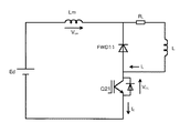
図5に電圧駆動型半導体素子としてIGBTを用いた電圧形インバータの従来例を示す。
これは、直流電圧源Ed、平滑用コンデンサCF 、IGBT素子Q11,Q12,Q21,Q22から構成され、例えばQ12とQ21をオンすることで正の直流電圧を、また、Q11とQ22をオンすることで負の直流電圧を出力するようになっている。出力電圧が正→負と交互に出力されることにより、交流電圧が出力され、これによって、負荷抵抗RL と負荷リアクトルLに負荷電流IL を流すようにしている。
【0003】
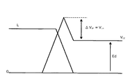
図6は図5の電圧形インバータでQ21がスイッチングするときの等価回路図であり、同図のLmは回路の配線インダクタンス、FDW11はQ11に内蔵されているフリーホィールダイオードを示す。図7に、Q21ターンオフ時のコレクタ−エミッタ間電圧VCEおよびコレクタ電流IC の波形を示す。
図6において、Q21がオン状態の時はEd→Lm→RL →L→Q21→Edの経路で電流が流れる。Q21がターンオフすると、Q21のコレクタ−エミッタ間電圧VCEが、図7のように上昇する。VCEが直流電圧Edに達しFDW11がオンすることによって、負荷電流IL はFDW11に転流して、コレクタ電流IC が図7のように減少する。この電流変化率(減少率)−di/dtにより、回路配線インダクタンスLmに誘起電圧VLm(=ΔVSP)が発生するため、Q21に対して図7に示すように、Ed+ΔVSPが印加される。
スパイク電圧ΔVSPはLm×(−di/dt)となるので、ΔVSPを減少させるためには、回路配線インダクタンスLmまたは電流変化率−di/dtを低減する必要がある。しかし、回路配線インダクタンスLmの低減には回路配線上の制約(制限)があるので、ΔVSPを減少させるには電流変化率−di/dtを低減させるのが一般的な方法である。
【0004】
図8に、電流変化率−di/dtを低減させる方法の従来例を示す。
これは、IGBTのゲート駆動回路を示すもので、ターンオフ時には図8のM−N15間にオフゲート用電源が接続される。そのとき、電流はゲート電源(M)→IGBTゲート入力容量(IGBTゲート−エミッタ間)→Rg(off)→TR2→ゲート電源(N15)のルートで流れる。この電流が流れるとIGBT入力容量に逆バイアス電圧が充電されることによって、IGBTがターンオフする。その際、ゲート抵抗Rg(off)を大きくすることにより、IGBT入力容量に対する充電時間を遅らせて、ゲート電圧を緩やかに変化させることができる。これにより、IGBTの電流変化率−di/dtが低減され、その結果、スパイク電圧ΔVSPを図9の点線で示すように低減することができる。
なお、オフ用ゲート電源の電圧値を小さくし、逆バイアス電圧を浅くすることで、ゲート電圧を緩やかに変化させることができる。これによっても、IGBTの電流変化率−di/dtが低減され、スパイク電圧ΔVSPを低減できる。
【0005】
【発明が解決しようとする課題】
上述のように、IGBTターンオフ時に、ゲート抵抗Rg(off)を大きくすることでスパイク電圧ΔVSPを低減できるが、図9に示すようにオン・オフ信号が入力されてからIGBTが動作するまでの時間遅れが増加するという問題がある。
また、逆バイアス電圧を浅くすることでも、スパイク電圧ΔVSPを低減できるが、逆バイアス電圧が浅いと、種々のノイズやゲート駆動回路の誤動作により、ゲート電圧がIGBTのしきい値電圧を越えやすくなるため、IGBTがオン(誤動作)しやすくなるという問題もある。
したがって、この発明の課題は素子ターンオフ時のスパイク電圧の低減,オン・オフ信号が入力されてからIGBTが動作するまでの時間短縮を図り、誤動作を防止することにある。
【0006】
【課題を解決するための手段】
このような課題を解決するため、請求項1の発明では、電圧駆動型半導体素子からなる電力変換装置に対し、
前記電圧駆動型半導体素子のスイッチングを制御する制御装置と、この制御装置からの信号に基づき電圧駆動型半導体素子を駆動する駆動回路と、電圧駆動型半導体素子のターンオフ時のゲート電圧を一定期間クランプするクランプ回路とを設け、
前記電圧駆動型半導体素子ターンオフ時のゲート電圧を、前記クランプ回路により逆バイアス電圧としきい値電圧との間の電圧に一定時間だけクランプし、その後は逆バイアス電圧に戻すことにより、電圧駆動型半導体素子ターンオフ時に発生するスパイク電圧の低減と、制御信号を受けてから素子がターンオフ開始するまでの時間短縮とを図るようにしている。
上記請求項1の発明においては、前記ゲート電圧をクランプする一定時間を、電圧駆動型半導体素子のスパイク電圧発生期間とし、素子が通常オフしている期間の誤動作防止を図ることができる(請求項2の発明)。
【0007】
【発明の実施の形態】
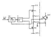
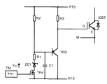
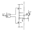
図1はこの発明の実施の形態を示す構成図、図2は図1で用いられるゲート電圧クランプ回路の具体例を示す回路図である。
すなわち、この発明は従来例に対しゲート電圧クランプ回路GCを付加して構成される。ゲート電圧クランプ回路GCとしては、例えば図2に示すような、トランジスタTR3、MOSFET素子TR4、ツェナーダイオードZD1、コンデンサC1、抵抗R1,R2,R3およびタイマーTM等からなる回路とすることができる。
【0008】
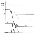
次に、図2の回路の動作について、図3を参照して説明する。なお、オフ用のゲート電源としては15Vの電源が接続されているものとし、逆バイアス電圧は−15Vであるとする。
いま、図3のオン・オフ信号がオンからオフに変わると、TR4が図示のように即座にオンし、TR3のベース−エミッタ間に電流が流れてこれがオンする。TR3がオンすると、IGBTのゲート−エミッタ間のコンデンサ(入力容量)が逆バイアス電圧に向かって充電を開始し、IGBTはターンオフ動作を開始する。そして、ZD1のツェナー電圧VZD1 に達するとTR3がオフし、IGBTの入力容量への充電が止まり、ゲート−エミッタ間の電圧がクランプされる。ここに、ツェナー電圧VZD1 の値は、ゲート電圧がしきい値電圧から逆バイアス電圧の間になるような値に設定するものとする。
【0009】
TR4のゲートにはタイマー回路TMが接続されており、したがって、TR4はオフ信号が入力されてからタイマー時間後にオフする。TR4がオフすると、ゲート電圧クランプ回路GCは切り離され、IGBTのゲート−エミッタ間電圧VGEは逆バイアス電圧(−15V)まで充電され、IGBTは完全なオフ状態となる。
以上のように、ここではIGBTのターンオフ時には、IGBTのゲート電圧は図3に示すように、逆バイアス電圧としきい値電圧との間の電圧値にクランプされるため、従来のターンオフ時(図3の点線参照)に比べてIGBTの入力容量に緩やかに充電が行なわれ、したがって図3に実線で示すように、IGBTの電流変化率−di/dtが低減され、スパイク電圧も抑制されることになる。
【0010】
図4はこの発明によってスパイク電圧も抑制する場合と、従来一般的に用いられるゲート抵抗の調整によってスパイク電圧を抑制する従来方式の場合とを比較説明するための波形図である。
同図に示すように、オン・オフ信号が入力されてからIGBTがターンオフ動作を開始するまでの時間が、この発明による場合はT1、従来方式の場合はT2で、T1<T2であることから、この発明による場合の方が動作遅れ時間の増加を抑制できることが分かる。
【0011】
また、ゲート電圧のクランプ時間を、電圧駆動型半導体素子のスパイク電圧発生期間とすれば、オフ時におけるIGBTの誤動作を防ぐことが可能となる。さらに、ゲート電圧クランプ期間中にIGBT誤動作によりこれがオンしてしまった場合でも、対向アームのIGBTはデッドタイム期間中でオフしているので、アーム短絡となるおそれもない。
【0012】
【発明の効果】
この発明によれば、ゲート電圧クランプ回路を設けて、ターンオフ動作中にゲート電圧を一定期間クランプし、その後は元に戻すことによってIGBTスイッチング動作を緩やかにし、かつ、入力信号からスイッチング動作までの遅れ時間を増加させることなく、スパイク電圧を抑制することができる。また、ゲート電圧をクランプする一定時間を、電圧駆動型半導体素子のスパイク電圧発生期間に限定することで、スパイク電圧の抑制効果だけでなく、IGBTターンオフおよび通常オフ時のIGBT誤動作によるアーム短絡を防ぐことができるという利点もある。
【図面の簡単な説明】
【図1】この発明の実施の形態を示す構成図である。
【図2】図1のゲート電圧クランプ回路の具体例を示す回路図である。
【図3】図2の動作説明図である。
【図4】スパイク電圧の抑制効果について、この発明によるものと従来方式とを比較して説明する説明図である。
【図5】IGBTを用いた電圧形インバータ主回路の一般例を示す回路図である。
【図6】図5で素子Q21が動作する場合を説明するための等価回路図である。
【図7】図6の動作説明図である。
【図8】ゲート駆動回路の従来例を示す回路図である。
【図9】図8の動作説明図である。
【符号の説明】
IF…インターフェイス回路、GC…ゲート電圧クランプ回路、TM…タイマー、TR1〜TR3…トランジスタ、TR4…FET、ZD1…ツェナーダイオード、Q11〜Q22,IGBT…スイッチ素子(絶縁ゲートバイポーラトランジスタ)、R…抵抗、C…コンデンサ、Ed…直流電圧源、L…リアクトル。[0001]
TECHNICAL FIELD OF THE INVENTION
The present invention relates to a gate drive circuit for a voltage-driven semiconductor device such as an IGBT (Insulated Gate Bipolar Transistor) constituting a power converter.
[0002]
[Prior art]
FIG. 5 shows a conventional example of a voltage-source inverter using an IGBT as a voltage-driven semiconductor element.
It comprises a DC voltage source Ed, a smoothing capacitor CF , and IGBT elements Q11, Q12, Q21, Q22. For example, turning on Q12 and Q21 turns on a positive DC voltage, and turning on Q11 and Q22. As a result, a negative DC voltage is output. When the output voltage is output to the positive → negative alternating, AC voltage is output, thereby, so that the load current I L in the load resistor R L and the load reactor L.
[0003]
FIG. 6 is an equivalent circuit diagram when Q21 switches in the voltage source inverter of FIG. 5. In FIG. 6, Lm denotes the wiring inductance of the circuit, and FDW11 denotes a free wheel diode built in Q11. 7, the collector when Q21 turns off - shows the waveform of the emitter voltage V CE and the collector current I C.
In FIG. 6, when Q21 is in the ON state, a current flows through the path of Ed → Lm → RL → L → Q21 → Ed. When Q21 is turned off, the collector of Q21 - emitter voltage V CE rises as shown in FIG. 7. By V CE is turned FDW11 reaches the DC voltage Ed, the load current I L is commutated to FDW11, the collector current I C decreases as shown in FIG. 7. Since the induced voltage V Lm (= ΔV SP ) is generated in the circuit wiring inductance Lm by the current change rate (decrease rate) -di / dt, Ed + ΔV SP is applied to Q21 as shown in FIG. .
Since the spike voltage ΔV SP is Lm × (−di / dt), it is necessary to reduce the circuit wiring inductance Lm or the current change rate −di / dt in order to reduce ΔV SP . However, since there is a restriction (limitation) on the circuit wiring in reducing the circuit wiring inductance Lm, it is a general method to reduce the current change rate -di / dt to reduce ΔV SP .
[0004]
FIG. 8 shows a conventional example of a method for reducing the current change rate -di / dt.
This shows a gate drive circuit of the IGBT, and an off-gate power supply is connected between M and N15 in FIG. 8 at the time of turn-off. At this time, the current flows in the route of gate power supply (M) → IGBT gate input capacitance (between IGBT gate and emitter) → Rg (off) → TR2 → gate power supply (N15). When this current flows, the IGBT input capacitor is charged with a reverse bias voltage, and the IGBT is turned off. At that time, by increasing the gate resistance Rg (off), the charging time for the IGBT input capacitance can be delayed, and the gate voltage can be gradually changed. Thereby, the current change rate -di / dt of the IGBT is reduced, and as a result, the spike voltage ΔV SP can be reduced as shown by the dotted line in FIG.
The gate voltage can be changed gradually by reducing the voltage value of the off gate power supply and decreasing the reverse bias voltage. Thus, the current change rate -di / dt of the IGBT is reduced, and the spike voltage ΔV SP can be reduced.
[0005]
[Problems to be solved by the invention]
As described above, when the IGBT is turned off, the spike voltage ΔV SP can be reduced by increasing the gate resistance Rg (off). However, as shown in FIG. 9, the time from when the on / off signal is input to when the IGBT operates is operated. There is a problem that a time delay increases.
The spike voltage ΔV SP can also be reduced by making the reverse bias voltage shallow, but if the reverse bias voltage is shallow, the gate voltage easily exceeds the threshold voltage of the IGBT due to various noises and malfunctions of the gate drive circuit. Therefore, there is a problem that the IGBT is easily turned on (malfunction).
SUMMARY OF THE INVENTION It is therefore an object of the present invention to reduce a spike voltage when an element is turned off, to shorten the time from when an on / off signal is input to when the IGBT operates, and to prevent malfunction.
[0006]
[Means for Solving the Problems]
In order to solve such a problem, the invention according to claim 1 relates to a power conversion device including a voltage-driven semiconductor element.
A control device for controlling the switching of the voltage-driven semiconductor device, a drive circuit for driving the voltage-driven semiconductor device based on a signal from the control device, and clamping of a gate voltage at the time of turn-off of the voltage-driven semiconductor device for a certain period of time And a clamp circuit for
The gate voltage at the time of turning off the voltage-driven semiconductor element is clamped by the clamp circuit to a voltage between a reverse bias voltage and a threshold voltage for a certain period of time, and thereafter, the voltage is returned to the reverse bias voltage. The spike voltage generated when the element is turned off is reduced, and the time from when the control signal is received to when the element starts turning off is reduced.
According to the first aspect of the present invention, the fixed time for clamping the gate voltage is defined as a spike voltage generation period of the voltage-driven semiconductor device, thereby preventing malfunction during a period in which the device is normally off. 2).
[0007]
BEST MODE FOR CARRYING OUT THE INVENTION
FIG. 1 is a block diagram showing an embodiment of the present invention, and FIG. 2 is a circuit diagram showing a specific example of a gate voltage clamp circuit used in FIG.
That is, the present invention is configured by adding a gate voltage clamp circuit GC to the conventional example. As the gate voltage clamp circuit GC, for example, a circuit including a transistor TR3, a MOSFET element TR4, a Zener diode ZD1, a capacitor C1, resistors R1, R2, R3, and a timer TM as shown in FIG. 2 can be used.
[0008]
Next, the operation of the circuit of FIG. 2 will be described with reference to FIG. It is assumed that a power supply of 15 V is connected as an off gate power supply, and the reverse bias voltage is -15 V.
Now, when the on / off signal in FIG. 3 changes from on to off, TR4 is turned on immediately as shown, and a current flows between the base and the emitter of TR3 to turn it on. When TR3 is turned on, the capacitor (input capacitance) between the gate and the emitter of the IGBT starts charging toward the reverse bias voltage, and the IGBT starts turning off. When the Zener voltage VZD1 of ZD1 is reached, TR3 is turned off, charging of the input capacitance of the IGBT is stopped, and the voltage between the gate and the emitter is clamped. Here, the value of the Zener voltage V ZD1 is set to a value such that the gate voltage is between the threshold voltage and the reverse bias voltage.
[0009]
A timer circuit TM is connected to the gate of TR4, so that TR4 turns off after a timer period from the input of the OFF signal. When TR4 is turned off, the gate voltage clamp circuit GC is disconnected, the gate-emitter voltage V GE of the IGBT is charged to the reverse bias voltage (−15 V), and the IGBT is completely turned off.
As described above, when the IGBT is turned off, the gate voltage of the IGBT is clamped to a voltage value between the reverse bias voltage and the threshold voltage as shown in FIG. (See dotted line in FIG. 3), the input capacitance of the IGBT is more slowly charged. Therefore, as shown by the solid line in FIG. 3, the current change rate -di / dt of the IGBT is reduced, and the spike voltage is suppressed. Become.
[0010]
FIG. 4 is a waveform chart for comparing and explaining the case where the spike voltage is suppressed by the present invention and the case of the conventional method which suppresses the spike voltage by adjusting the gate resistance generally used in the related art.
As shown in the figure, the time from the input of the on / off signal to the start of the turn-off operation of the IGBT is T1 in the case of the present invention, T2 in the case of the conventional method, and T1 <T2. It can be seen that the case according to the present invention can suppress an increase in the operation delay time.
[0011]
In addition, if the clamp time of the gate voltage is set to the spike voltage generation period of the voltage-driven semiconductor device, it is possible to prevent the IGBT from malfunctioning when it is off. Further, even if the IGBT is turned on due to a malfunction of the IGBT during the gate voltage clamp period, the IGBT of the opposing arm is turned off during the dead time period, so that there is no danger of arm short-circuit.
[0012]
【The invention's effect】
According to the present invention, the gate voltage clamping circuit is provided, the gate voltage is clamped for a certain period during the turn-off operation, and thereafter, the gate voltage is restored to the original state, so that the IGBT switching operation is moderated, and the delay from the input signal to the switching operation is delayed. The spike voltage can be suppressed without increasing the time. In addition, by limiting the fixed time for clamping the gate voltage to the spike voltage generation period of the voltage-driven semiconductor element, not only the effect of suppressing the spike voltage but also the arm short-circuit due to the IGBT turn-off and the IGBT malfunction during the normal off is prevented. There is also the advantage that it can be done.
[Brief description of the drawings]
FIG. 1 is a configuration diagram showing an embodiment of the present invention.
FIG. 2 is a circuit diagram showing a specific example of the gate voltage clamp circuit of FIG.
FIG. 3 is an operation explanatory diagram of FIG. 2;
FIG. 4 is an explanatory diagram for explaining the effect of suppressing the spike voltage by comparing the effect according to the present invention with the conventional method.
FIG. 5 is a circuit diagram showing a general example of a voltage source inverter main circuit using an IGBT.
FIG. 6 is an equivalent circuit diagram for explaining a case where an element Q21 operates in FIG.
FIG. 7 is an operation explanatory diagram of FIG. 6;
FIG. 8 is a circuit diagram showing a conventional example of a gate drive circuit.
FIG. 9 is an operation explanatory diagram of FIG. 8;
[Explanation of symbols]
IF: Interface circuit, GC: Gate voltage clamp circuit, TM: Timer, TR1 to TR3: Transistor, TR4: FET, ZD1: Zener diode, Q11 to Q22, IGBT: Switch element (insulated gate bipolar transistor), R: Resistance, C: condenser, Ed: DC voltage source, L: reactor.
Claims (2)
前記電圧駆動型半導体素子のスイッチングを制御する制御装置と、この制御装置からの信号に基づき電圧駆動型半導体素子を駆動する駆動回路と、電圧駆動型半導体素子のターンオフ時のゲート電圧を一定期間クランプするクランプ回路とを設け、
前記電圧駆動型半導体素子ターンオフ時のゲート電圧を、前記クランプ回路により逆バイアス電圧としきい値電圧との間の電圧に一定時間だけクランプし、その後は逆バイアス電圧に戻すことにより、電圧駆動型半導体素子ターンオフ時に発生するスパイク電圧の低減と、制御信号を受けてから素子がターンオフ開始するまでの時間短縮とを図ることを特徴とする電圧駆動型半導体素子のゲート駆動回路。For power converters consisting of voltage-driven semiconductor elements,
A control device for controlling the switching of the voltage-driven semiconductor device, a drive circuit for driving the voltage-driven semiconductor device based on a signal from the control device, and clamping of a gate voltage at the time of turn-off of the voltage-driven semiconductor device for a certain period of time And a clamp circuit for
The gate voltage at the time of turning off the voltage-driven semiconductor element is clamped by the clamp circuit to a voltage between a reverse bias voltage and a threshold voltage for a certain period of time, and thereafter, the voltage is returned to the reverse bias voltage. A gate drive circuit for a voltage-driven semiconductor device, characterized in that a spike voltage generated when the device is turned off is reduced, and a time from when a control signal is received to when the device starts to turn off is reduced.
Priority Applications (1)
| Application Number | Priority Date | Filing Date | Title |
|---|---|---|---|
| JP19511098A JP3568024B2 (en) | 1998-06-26 | 1998-06-26 | Gate drive circuit for voltage driven semiconductor device |
Applications Claiming Priority (1)
| Application Number | Priority Date | Filing Date | Title |
|---|---|---|---|
| JP19511098A JP3568024B2 (en) | 1998-06-26 | 1998-06-26 | Gate drive circuit for voltage driven semiconductor device |
Publications (2)
| Publication Number | Publication Date |
|---|---|
| JP2000014127A JP2000014127A (en) | 2000-01-14 |
| JP3568024B2 true JP3568024B2 (en) | 2004-09-22 |
Family
ID=16335674
Family Applications (1)
| Application Number | Title | Priority Date | Filing Date |
|---|---|---|---|
| JP19511098A Expired - Fee Related JP3568024B2 (en) | 1998-06-26 | 1998-06-26 | Gate drive circuit for voltage driven semiconductor device |
Country Status (1)
| Country | Link |
|---|---|
| JP (1) | JP3568024B2 (en) |
Cited By (1)
| Publication number | Priority date | Publication date | Assignee | Title |
|---|---|---|---|---|
| JP2021005950A (en) * | 2019-06-26 | 2021-01-14 | 株式会社デンソー | Transistor drive circuit and gate voltage control method of transistor |
Families Citing this family (5)
| Publication number | Priority date | Publication date | Assignee | Title |
|---|---|---|---|---|
| JP4240140B1 (en) | 2007-09-10 | 2009-03-18 | トヨタ自動車株式会社 | Power supply apparatus and driving method thereof |
| JP5761215B2 (en) | 2013-01-21 | 2015-08-12 | 株式会社デンソー | Gate drive circuit |
| CN106452404B (en) * | 2016-07-25 | 2023-06-06 | 天津理工大学 | Active gate control circuit and IGBT electromagnetic interference suppression method thereof |
| CN115632642B (en) * | 2022-12-21 | 2023-03-10 | 杭州飞仕得科技股份有限公司 | IGBT turn-off voltage spike suppression circuit and related equipment |
| CN116722729B (en) * | 2023-08-09 | 2023-11-03 | 苏州贝克微电子股份有限公司 | Circuit for reducing turn-off peak voltage of switching tube |
-
1998
- 1998-06-26 JP JP19511098A patent/JP3568024B2/en not_active Expired - Fee Related
Cited By (1)
| Publication number | Priority date | Publication date | Assignee | Title |
|---|---|---|---|---|
| JP2021005950A (en) * | 2019-06-26 | 2021-01-14 | 株式会社デンソー | Transistor drive circuit and gate voltage control method of transistor |
Also Published As
| Publication number | Publication date |
|---|---|
| JP2000014127A (en) | 2000-01-14 |
Similar Documents
| Publication | Publication Date | Title |
|---|---|---|
| JP4432215B2 (en) | Semiconductor switching element gate drive circuit | |
| JP3339311B2 (en) | Driver circuit for self-extinguishing semiconductor device | |
| JP4343897B2 (en) | Power converter | |
| US5107151A (en) | Switching circuit employing electronic devices in series with an inductor to avoid commutation breakdown and extending the current range of switching circuits by using igbt devices in place of mosfets | |
| JP3577807B2 (en) | Driver circuit for self-extinguishing semiconductor device | |
| US20020191426A1 (en) | Inrush current limiting circuit, power source device and power conversion device | |
| JP4120329B2 (en) | Voltage-driven semiconductor device gate drive device | |
| JP3052792B2 (en) | Inverter device | |
| US7248093B2 (en) | Bipolar bootstrap top switch gate drive for half-bridge semiconductor power topologies | |
| JP3568024B2 (en) | Gate drive circuit for voltage driven semiconductor device | |
| JP4100134B2 (en) | Inverter | |
| JP2002125363A (en) | Gate drive circuit of power semiconductor element | |
| JP4506276B2 (en) | Drive circuit for self-extinguishing semiconductor device | |
| JP3532377B2 (en) | Gate drive circuit for voltage driven switch element | |
| WO2023135885A1 (en) | Driving device of semiconductor switching element and power conversion device | |
| KR20000006533A (en) | Inverter apparatus | |
| WO2023062745A1 (en) | Driving circuit for power semiconductor device, power semiconductor module, and power converter | |
| JP2007104739A (en) | Drive circuit of power semiconductor module | |
| JPH1169778A (en) | Gate drive circuit in power converter | |
| JPH10209832A (en) | Semiconductor switch circuit | |
| JP2004260981A (en) | Power converting device and electric machine system utilizing it | |
| JP2000139071A (en) | Gate driving circuit for power converter | |
| JP3558324B2 (en) | Gate drive device of voltage drive type device | |
| JP3724255B2 (en) | Gate drive circuit for voltage driven semiconductor device | |
| JP2003143831A (en) | Gate drive circuit |
Legal Events
| Date | Code | Title | Description |
|---|---|---|---|
| RD03 | Notification of appointment of power of attorney |
Free format text: JAPANESE INTERMEDIATE CODE: A7423 Effective date: 20031201 |
|
| RD04 | Notification of resignation of power of attorney |
Free format text: JAPANESE INTERMEDIATE CODE: A7424 Effective date: 20040205 |
|
| A977 | Report on retrieval |
Free format text: JAPANESE INTERMEDIATE CODE: A971007 Effective date: 20040302 |
|
| A131 | Notification of reasons for refusal |
Free format text: JAPANESE INTERMEDIATE CODE: A131 Effective date: 20040311 |
|
| TRDD | Decision of grant or rejection written | ||
| A01 | Written decision to grant a patent or to grant a registration (utility model) |
Free format text: JAPANESE INTERMEDIATE CODE: A01 Effective date: 20040527 |
|
| A61 | First payment of annual fees (during grant procedure) |
Free format text: JAPANESE INTERMEDIATE CODE: A61 Effective date: 20040609 |
|
| R150 | Certificate of patent or registration of utility model |
Free format text: JAPANESE INTERMEDIATE CODE: R150 |
|
| R250 | Receipt of annual fees |
Free format text: JAPANESE INTERMEDIATE CODE: R250 |
|
| FPAY | Renewal fee payment (event date is renewal date of database) |
Free format text: PAYMENT UNTIL: 20080625 Year of fee payment: 4 |
|
| FPAY | Renewal fee payment (event date is renewal date of database) |
Free format text: PAYMENT UNTIL: 20090625 Year of fee payment: 5 |
|
| FPAY | Renewal fee payment (event date is renewal date of database) |
Free format text: PAYMENT UNTIL: 20100625 Year of fee payment: 6 |
|
| FPAY | Renewal fee payment (event date is renewal date of database) |
Free format text: PAYMENT UNTIL: 20100625 Year of fee payment: 6 |
|
| FPAY | Renewal fee payment (event date is renewal date of database) |
Free format text: PAYMENT UNTIL: 20110625 Year of fee payment: 7 |
|
| S531 | Written request for registration of change of domicile |
Free format text: JAPANESE INTERMEDIATE CODE: R313531 |
|
| FPAY | Renewal fee payment (event date is renewal date of database) |
Free format text: PAYMENT UNTIL: 20110625 Year of fee payment: 7 |
|
| R350 | Written notification of registration of transfer |
Free format text: JAPANESE INTERMEDIATE CODE: R350 |
|
| FPAY | Renewal fee payment (event date is renewal date of database) |
Free format text: PAYMENT UNTIL: 20110625 Year of fee payment: 7 |
|
| S111 | Request for change of ownership or part of ownership |
Free format text: JAPANESE INTERMEDIATE CODE: R313111 |
|
| R350 | Written notification of registration of transfer |
Free format text: JAPANESE INTERMEDIATE CODE: R350 |
|
| FPAY | Renewal fee payment (event date is renewal date of database) |
Free format text: PAYMENT UNTIL: 20120625 Year of fee payment: 8 |
|
| FPAY | Renewal fee payment (event date is renewal date of database) |
Free format text: PAYMENT UNTIL: 20130625 Year of fee payment: 9 |
|
| R250 | Receipt of annual fees |
Free format text: JAPANESE INTERMEDIATE CODE: R250 |
|
| R250 | Receipt of annual fees |
Free format text: JAPANESE INTERMEDIATE CODE: R250 |
|
| R250 | Receipt of annual fees |
Free format text: JAPANESE INTERMEDIATE CODE: R250 |
|
| R250 | Receipt of annual fees |
Free format text: JAPANESE INTERMEDIATE CODE: R250 |
|
| R250 | Receipt of annual fees |
Free format text: JAPANESE INTERMEDIATE CODE: R250 |
|
| LAPS | Cancellation because of no payment of annual fees |