JP2022540468A - 3d半導体メモリ構造体を形成する方法、構造体 - Google Patents
3d半導体メモリ構造体を形成する方法、構造体 Download PDFInfo
- Publication number
- JP2022540468A JP2022540468A JP2022501110A JP2022501110A JP2022540468A JP 2022540468 A JP2022540468 A JP 2022540468A JP 2022501110 A JP2022501110 A JP 2022501110A JP 2022501110 A JP2022501110 A JP 2022501110A JP 2022540468 A JP2022540468 A JP 2022540468A
- Authority
- JP
- Japan
- Prior art keywords
- chip
- memory
- hardware accelerator
- hbm
- substrate
- Prior art date
- Legal status (The legal status is an assumption and is not a legal conclusion. Google has not performed a legal analysis and makes no representation as to the accuracy of the status listed.)
- Granted
Links
Images



Classifications
-
- G—PHYSICS
- G11—INFORMATION STORAGE
- G11C—STATIC STORES
- G11C5/00—Details of stores covered by group G11C11/00
- G11C5/02—Disposition of storage elements, e.g. in the form of a matrix array
- G11C5/025—Geometric lay-out considerations of storage- and peripheral-blocks in a semiconductor storage device
-
- H—ELECTRICITY
- H10—SEMICONDUCTOR DEVICES; ELECTRIC SOLID-STATE DEVICES NOT OTHERWISE PROVIDED FOR
- H10D—INORGANIC ELECTRIC SEMICONDUCTOR DEVICES
- H10D88/00—Three-dimensional [3D] integrated devices
-
- H—ELECTRICITY
- H10—SEMICONDUCTOR DEVICES; ELECTRIC SOLID-STATE DEVICES NOT OTHERWISE PROVIDED FOR
- H10B—ELECTRONIC MEMORY DEVICES
- H10B63/00—Resistance change memory devices, e.g. resistive RAM [ReRAM] devices
- H10B63/80—Arrangements comprising multiple bistable or multi-stable switching components of the same type on a plane parallel to the substrate, e.g. cross-point arrays
- H10B63/84—Arrangements comprising multiple bistable or multi-stable switching components of the same type on a plane parallel to the substrate, e.g. cross-point arrays arranged in a direction perpendicular to the substrate, e.g. 3D cell arrays
- H10B63/845—Arrangements comprising multiple bistable or multi-stable switching components of the same type on a plane parallel to the substrate, e.g. cross-point arrays arranged in a direction perpendicular to the substrate, e.g. 3D cell arrays the switching components being connected to a common vertical conductor
-
- H—ELECTRICITY
- H10—SEMICONDUCTOR DEVICES; ELECTRIC SOLID-STATE DEVICES NOT OTHERWISE PROVIDED FOR
- H10W—GENERIC PACKAGES, INTERCONNECTIONS, CONNECTORS OR OTHER CONSTRUCTIONAL DETAILS OF DEVICES COVERED BY CLASS H10
- H10W90/00—Package configurations
-
- G—PHYSICS
- G06—COMPUTING OR CALCULATING; COUNTING
- G06N—COMPUTING ARRANGEMENTS BASED ON SPECIFIC COMPUTATIONAL MODELS
- G06N3/00—Computing arrangements based on biological models
- G06N3/02—Neural networks
- G06N3/06—Physical realisation, i.e. hardware implementation of neural networks, neurons or parts of neurons
- G06N3/063—Physical realisation, i.e. hardware implementation of neural networks, neurons or parts of neurons using electronic means
-
- G—PHYSICS
- G06—COMPUTING OR CALCULATING; COUNTING
- G06N—COMPUTING ARRANGEMENTS BASED ON SPECIFIC COMPUTATIONAL MODELS
- G06N3/00—Computing arrangements based on biological models
- G06N3/02—Neural networks
- G06N3/08—Learning methods
-
- G—PHYSICS
- G11—INFORMATION STORAGE
- G11C—STATIC STORES
- G11C11/00—Digital stores characterised by the use of particular electric or magnetic storage elements; Storage elements therefor
- G11C11/54—Digital stores characterised by the use of particular electric or magnetic storage elements; Storage elements therefor using elements simulating biological cells, e.g. neuron
-
- H—ELECTRICITY
- H10—SEMICONDUCTOR DEVICES; ELECTRIC SOLID-STATE DEVICES NOT OTHERWISE PROVIDED FOR
- H10W—GENERIC PACKAGES, INTERCONNECTIONS, CONNECTORS OR OTHER CONSTRUCTIONAL DETAILS OF DEVICES COVERED BY CLASS H10
- H10W70/00—Package substrates; Interposers; Redistribution layers [RDL]
- H10W70/60—Insulating or insulated package substrates; Interposers; Redistribution layers
- H10W70/62—Insulating or insulated package substrates; Interposers; Redistribution layers characterised by their interconnections
- H10W70/63—Vias, e.g. via plugs
-
- H—ELECTRICITY
- H10—SEMICONDUCTOR DEVICES; ELECTRIC SOLID-STATE DEVICES NOT OTHERWISE PROVIDED FOR
- H10W—GENERIC PACKAGES, INTERCONNECTIONS, CONNECTORS OR OTHER CONSTRUCTIONAL DETAILS OF DEVICES COVERED BY CLASS H10
- H10W70/00—Package substrates; Interposers; Redistribution layers [RDL]
- H10W70/60—Insulating or insulated package substrates; Interposers; Redistribution layers
- H10W70/62—Insulating or insulated package substrates; Interposers; Redistribution layers characterised by their interconnections
- H10W70/65—Shapes or dispositions of interconnections
- H10W70/654—Top-view layouts
- H10W70/656—Fan-in layouts
-
- H—ELECTRICITY
- H10—SEMICONDUCTOR DEVICES; ELECTRIC SOLID-STATE DEVICES NOT OTHERWISE PROVIDED FOR
- H10W—GENERIC PACKAGES, INTERCONNECTIONS, CONNECTORS OR OTHER CONSTRUCTIONAL DETAILS OF DEVICES COVERED BY CLASS H10
- H10W72/00—Interconnections or connectors in packages
- H10W72/071—Connecting or disconnecting
- H10W72/072—Connecting or disconnecting of bump connectors
-
- H—ELECTRICITY
- H10—SEMICONDUCTOR DEVICES; ELECTRIC SOLID-STATE DEVICES NOT OTHERWISE PROVIDED FOR
- H10W—GENERIC PACKAGES, INTERCONNECTIONS, CONNECTORS OR OTHER CONSTRUCTIONAL DETAILS OF DEVICES COVERED BY CLASS H10
- H10W72/00—Interconnections or connectors in packages
- H10W72/071—Connecting or disconnecting
- H10W72/072—Connecting or disconnecting of bump connectors
- H10W72/07251—Connecting or disconnecting of bump connectors characterised by changes in properties of the bump connectors during connecting
- H10W72/07254—Connecting or disconnecting of bump connectors characterised by changes in properties of the bump connectors during connecting changes in dispositions
-
- H—ELECTRICITY
- H10—SEMICONDUCTOR DEVICES; ELECTRIC SOLID-STATE DEVICES NOT OTHERWISE PROVIDED FOR
- H10W—GENERIC PACKAGES, INTERCONNECTIONS, CONNECTORS OR OTHER CONSTRUCTIONAL DETAILS OF DEVICES COVERED BY CLASS H10
- H10W72/00—Interconnections or connectors in packages
- H10W72/071—Connecting or disconnecting
- H10W72/073—Connecting or disconnecting of die-attach connectors
-
- H—ELECTRICITY
- H10—SEMICONDUCTOR DEVICES; ELECTRIC SOLID-STATE DEVICES NOT OTHERWISE PROVIDED FOR
- H10W—GENERIC PACKAGES, INTERCONNECTIONS, CONNECTORS OR OTHER CONSTRUCTIONAL DETAILS OF DEVICES COVERED BY CLASS H10
- H10W72/00—Interconnections or connectors in packages
- H10W72/20—Bump connectors, e.g. solder bumps or copper pillars; Dummy bumps; Thermal bumps
- H10W72/221—Structures or relative sizes
- H10W72/222—Multilayered bumps, e.g. a coating on top and side surfaces of a bump core
-
- H—ELECTRICITY
- H10—SEMICONDUCTOR DEVICES; ELECTRIC SOLID-STATE DEVICES NOT OTHERWISE PROVIDED FOR
- H10W—GENERIC PACKAGES, INTERCONNECTIONS, CONNECTORS OR OTHER CONSTRUCTIONAL DETAILS OF DEVICES COVERED BY CLASS H10
- H10W72/00—Interconnections or connectors in packages
- H10W72/20—Bump connectors, e.g. solder bumps or copper pillars; Dummy bumps; Thermal bumps
- H10W72/241—Dispositions, e.g. layouts
- H10W72/247—Dispositions of multiple bumps
-
- H—ELECTRICITY
- H10—SEMICONDUCTOR DEVICES; ELECTRIC SOLID-STATE DEVICES NOT OTHERWISE PROVIDED FOR
- H10W—GENERIC PACKAGES, INTERCONNECTIONS, CONNECTORS OR OTHER CONSTRUCTIONAL DETAILS OF DEVICES COVERED BY CLASS H10
- H10W72/00—Interconnections or connectors in packages
- H10W72/20—Bump connectors, e.g. solder bumps or copper pillars; Dummy bumps; Thermal bumps
- H10W72/251—Materials
- H10W72/252—Materials comprising solid metals or solid metalloids, e.g. PbSn, Ag or Cu
-
- H—ELECTRICITY
- H10—SEMICONDUCTOR DEVICES; ELECTRIC SOLID-STATE DEVICES NOT OTHERWISE PROVIDED FOR
- H10W—GENERIC PACKAGES, INTERCONNECTIONS, CONNECTORS OR OTHER CONSTRUCTIONAL DETAILS OF DEVICES COVERED BY CLASS H10
- H10W72/00—Interconnections or connectors in packages
- H10W72/20—Bump connectors, e.g. solder bumps or copper pillars; Dummy bumps; Thermal bumps
- H10W72/261—Functions other than electrical connecting
- H10W72/263—Providing mechanical bonding or support, e.g. dummy bumps
-
- H—ELECTRICITY
- H10—SEMICONDUCTOR DEVICES; ELECTRIC SOLID-STATE DEVICES NOT OTHERWISE PROVIDED FOR
- H10W—GENERIC PACKAGES, INTERCONNECTIONS, CONNECTORS OR OTHER CONSTRUCTIONAL DETAILS OF DEVICES COVERED BY CLASS H10
- H10W72/00—Interconnections or connectors in packages
- H10W72/20—Bump connectors, e.g. solder bumps or copper pillars; Dummy bumps; Thermal bumps
- H10W72/261—Functions other than electrical connecting
- H10W72/267—Multiple bump connectors having different functions
-
- H—ELECTRICITY
- H10—SEMICONDUCTOR DEVICES; ELECTRIC SOLID-STATE DEVICES NOT OTHERWISE PROVIDED FOR
- H10W—GENERIC PACKAGES, INTERCONNECTIONS, CONNECTORS OR OTHER CONSTRUCTIONAL DETAILS OF DEVICES COVERED BY CLASS H10
- H10W72/00—Interconnections or connectors in packages
- H10W72/90—Bond pads, in general
- H10W72/941—Dispositions of bond pads
- H10W72/942—Dispositions of bond pads relative to underlying supporting features, e.g. bond pads, RDLs or vias
-
- H—ELECTRICITY
- H10—SEMICONDUCTOR DEVICES; ELECTRIC SOLID-STATE DEVICES NOT OTHERWISE PROVIDED FOR
- H10W—GENERIC PACKAGES, INTERCONNECTIONS, CONNECTORS OR OTHER CONSTRUCTIONAL DETAILS OF DEVICES COVERED BY CLASS H10
- H10W74/00—Encapsulations, e.g. protective coatings
- H10W74/10—Encapsulations, e.g. protective coatings characterised by their shape or disposition
- H10W74/15—Encapsulations, e.g. protective coatings characterised by their shape or disposition on active surfaces of flip-chip devices, e.g. underfills
-
- H—ELECTRICITY
- H10—SEMICONDUCTOR DEVICES; ELECTRIC SOLID-STATE DEVICES NOT OTHERWISE PROVIDED FOR
- H10W—GENERIC PACKAGES, INTERCONNECTIONS, CONNECTORS OR OTHER CONSTRUCTIONAL DETAILS OF DEVICES COVERED BY CLASS H10
- H10W90/00—Package configurations
- H10W90/20—Configurations of stacked chips
- H10W90/28—Configurations of stacked chips the stacked chips having different sizes, e.g. chip stacks having a pyramidal shape
-
- H—ELECTRICITY
- H10—SEMICONDUCTOR DEVICES; ELECTRIC SOLID-STATE DEVICES NOT OTHERWISE PROVIDED FOR
- H10W—GENERIC PACKAGES, INTERCONNECTIONS, CONNECTORS OR OTHER CONSTRUCTIONAL DETAILS OF DEVICES COVERED BY CLASS H10
- H10W90/00—Package configurations
- H10W90/20—Configurations of stacked chips
- H10W90/297—Configurations of stacked chips characterised by the through-semiconductor vias [TSVs] in the stacked chips
-
- H—ELECTRICITY
- H10—SEMICONDUCTOR DEVICES; ELECTRIC SOLID-STATE DEVICES NOT OTHERWISE PROVIDED FOR
- H10W—GENERIC PACKAGES, INTERCONNECTIONS, CONNECTORS OR OTHER CONSTRUCTIONAL DETAILS OF DEVICES COVERED BY CLASS H10
- H10W90/00—Package configurations
- H10W90/701—Package configurations characterised by the relative positions of pads or connectors relative to package parts
- H10W90/721—Package configurations characterised by the relative positions of pads or connectors relative to package parts of bump connectors
- H10W90/722—Package configurations characterised by the relative positions of pads or connectors relative to package parts of bump connectors between stacked chips
-
- H—ELECTRICITY
- H10—SEMICONDUCTOR DEVICES; ELECTRIC SOLID-STATE DEVICES NOT OTHERWISE PROVIDED FOR
- H10W—GENERIC PACKAGES, INTERCONNECTIONS, CONNECTORS OR OTHER CONSTRUCTIONAL DETAILS OF DEVICES COVERED BY CLASS H10
- H10W90/00—Package configurations
- H10W90/701—Package configurations characterised by the relative positions of pads or connectors relative to package parts
- H10W90/721—Package configurations characterised by the relative positions of pads or connectors relative to package parts of bump connectors
- H10W90/724—Package configurations characterised by the relative positions of pads or connectors relative to package parts of bump connectors between a chip and a stacked insulating package substrate, interposer or RDL
Landscapes
- Engineering & Computer Science (AREA)
- Microelectronics & Electronic Packaging (AREA)
- Semiconductor Memories (AREA)
- Dram (AREA)
Abstract
Description
Claims (24)
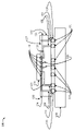
- 3次元(3D)半導体メモリ構造体であって、
メモリおよびシリコン貫通ビア(TSV)を含むメモリ・チップと、
前記チップ上に配列され、前記チップに結合されたハードウェア・アクセラレータと、
前記3D半導体メモリ構造体および前記ハードウェア・アクセラレータの下に配列され、前記TSVと、前記メモリ・チップおよび前記ハードウェア・アクセラレータの外部入力部および出力部とに取り付けられた基板と
を含む、3次元(3D)半導体メモリ構造体。 - 前記ハードウェア・アクセラレータが、前記メモリ・チップに対面して結合される、請求項1に記載の構造体。
- 前記TSVが、前記メモリ・チップの周囲に配列される、請求項2に記載の構造体。
- 前記メモリ・チップおよび前記ハードウェア・アクセラレータは、前記基板が取り付けられる中間構造体体を形成するように結合される、請求項2に記載の構造体。
- 前記基板が、事前にはんだ付けされたラミネートを含むパッケージング基板である、請求項2に記載の構造体。
- 前記メモリ・チップが、スタティック・ランダム・アクセス・メモリを含む、請求項2に記載の構造体。
- 前記基板に結合され、メモリ動作を実行するように構成された補助高帯域幅メモリ(HBM)をさらに含む、請求項2に記載の構造体。
- 前記補助HBMが、事前にはんだ付けされたラミネートを使用して前記基板に結合される、請求項7に記載の構造体。
- 前記メモリ・チップが、前記メモリ動作を制御するためのメモリ・コントローラをさらに含む、請求項8に記載の構造体。
- 前記メモリ・チップが、HBM PHYおよびHBMメモリ・コントローラを
さらに含み、前記HBM PHYおよび前記HBMメモリ・コントローラが、前記補助HBMをサポートし、バック・エンド・オブ・ライン(BEOL)金属ラインを使用して前記補助HBMに直接電気的に結合される、請求項8に記載の構造体。 - 前記HBM PHYおよび前記HBMメモリ・コントローラが、ウェハのBEOLの中間層誘電体層に配置される、請求項10に記載の構造体。
- 前記TSVが、前記メモリ・チップの周囲領域を通過する、請求項2に記載の構造体。
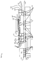
- 前記メモリ・チップと前記ハードウェア・アクセラレータとの間に配列され、前記ハードウェア・アクセラレータに対面して結合されたアナログ・チップを含み、前記基板が、前記構造体、前記ハードウェア・アクセラレータ、および前記アナログ・チップの下にある、請求項1に記載の構造体。
- 前記アナログ・チップが、Cuピラーおよびはんだキャップを使用して前記ハードウェア・アクセラレータに結合される、請求項13に記載の構造体。
- 前記アナログ・チップには、TSVがない、請求項13に記載の構造体。
- 前記アナログ・チップが、1つまたは複数のTSVを含む、請求項13に記載の構造体。
- 前記ハードウェア・アクセラレータが、銅対銅ボンドで使用される銅ピラーによって前記メモリ・チップに結合される、請求項13に記載の構造体。
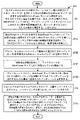
- 3次元(3D)半導体メモリ構造体を形成するための方法であって、
メモリおよびシリコン貫通ビア(TSV)を含むメモリ・チップを受け取るステップと、
ハードウェア・アクセラレータを、前記メモリ・チップに結合させるように前記メモリ・チップ上に配列するステップと、
基板を、前記3D半導体メモリ構造体および前記ハードウェア・アクセラレータの下に配列し、前記TSVと、前記メモリ・チップおよび前記ハードウェア・アクセラレータの外部入力部および出力部とに取り付けるステップと
を含む、方法。 - 前記ハードウェア・アクセラレータが、前記メモリ・チップに対面して結合される、請求項18に記載の方法。
- 前記TSVが、前記メモリ・チップの周囲に配列される、請求項19に記載の方法。
- 前記チップおよび前記ハードウェア・アクセラレータは、前記基板が取り付けられる中間構造体体を形成するように結合される、請求項19に記載の方法。
- 前記チップによりメモリ動作を実行するように構成された補助高帯域幅メモリ(HBM)を前記基板に結合させるステップをさらに含む、請求項19に記載の方法。
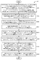
- 前記方法が、
アナログ・チップを、前記メモリ・チップと前記ハードウェア・アクセラレータとの間に配列し、前記ハードウェア・アクセラレータに対面して結合させるステップ
をさらに含み、
前記基板が、前記構造体、前記ハードウェア・アクセラレータ、および前記アナログ・チップの下に配列される、請求項18に記載の方法。 - 前記配列するステップの前に前記アナログ・チップを薄くするステップをさらに含む、請求項23に記載の方法。
Applications Claiming Priority (3)
| Application Number | Priority Date | Filing Date | Title |
|---|---|---|---|
| US16/515,877 US11211378B2 (en) | 2019-07-18 | 2019-07-18 | Heterogeneous integration structure for artificial intelligence computing |
| US16/515,877 | 2019-07-18 | ||
| PCT/IB2020/055605 WO2021009580A1 (en) | 2019-07-18 | 2020-06-16 | Heterogeneous integration structure for artificial intelligence computing |
Publications (2)
| Publication Number | Publication Date |
|---|---|
| JP2022540468A true JP2022540468A (ja) | 2022-09-15 |
| JP7442616B2 JP7442616B2 (ja) | 2024-03-04 |
Family
ID=74210225
Family Applications (1)
| Application Number | Title | Priority Date | Filing Date |
|---|---|---|---|
| JP2022501110A Active JP7442616B2 (ja) | 2019-07-18 | 2020-06-16 | 3d半導体メモリ構造体を形成する方法、構造体 |
Country Status (6)
| Country | Link |
|---|---|
| US (1) | US11211378B2 (ja) |
| JP (1) | JP7442616B2 (ja) |
| CN (1) | CN114072781B (ja) |
| DE (1) | DE112020002861T5 (ja) |
| GB (1) | GB2600585B (ja) |
| WO (1) | WO2021009580A1 (ja) |
Cited By (1)
| Publication number | Priority date | Publication date | Assignee | Title |
|---|---|---|---|---|
| US20230230901A1 (en) * | 2022-01-10 | 2023-07-20 | International Business Machines Corporation | TSV and Backside Power Distribution Structure |
Families Citing this family (4)
| Publication number | Priority date | Publication date | Assignee | Title |
|---|---|---|---|---|
| US12327175B2 (en) * | 2020-08-06 | 2025-06-10 | Micron Technology, Inc. | Collaborative sensor data processing by deep learning accelerators with integrated random access memory |
| US11791326B2 (en) | 2021-05-10 | 2023-10-17 | International Business Machines Corporation | Memory and logic chip stack with a translator chip |
| US11887908B2 (en) * | 2021-12-21 | 2024-01-30 | International Business Machines Corporation | Electronic package structure with offset stacked chips and top and bottom side cooling lid |
| US12581663B2 (en) | 2022-12-22 | 2026-03-17 | International Business Machines Corporation | Heterogeneous integration structure with voltage regulation |
Citations (8)
| Publication number | Priority date | Publication date | Assignee | Title |
|---|---|---|---|---|
| JP2005217388A (ja) * | 2004-01-30 | 2005-08-11 | Phoenix Precision Technology Corp | 半導体パッケージ基板のプリ半田構造及びその製法 |
| JP2008010859A (ja) * | 2006-06-02 | 2008-01-17 | Renesas Technology Corp | 半導体装置 |
| JP2015507843A (ja) * | 2011-12-22 | 2015-03-12 | インテル・コーポレーション | ウィンドウインタポーザを有する3d集積回路パッケージ |
| WO2016199437A1 (ja) * | 2015-06-12 | 2016-12-15 | 株式会社ソシオネクスト | 半導体装置 |
| JP2018010920A (ja) * | 2016-07-12 | 2018-01-18 | 富士通株式会社 | 半導体装置及びその製造方法 |
| JP2018022903A (ja) * | 2001-03-02 | 2018-02-08 | クゥアルコム・インコーポレイテッドQualcomm Incorporated | 混合アナログおよびデジタル集積回路 |
| US20180176006A1 (en) * | 2016-12-16 | 2018-06-21 | Intel Corporation | Active interposer for localized programmable integrated circuit reconfiguration |
| US20180286826A1 (en) * | 2017-03-29 | 2018-10-04 | Xilinx, Inc. | Methods of interconnect for high density 2.5d and 3d integration |
Family Cites Families (19)
| Publication number | Priority date | Publication date | Assignee | Title |
|---|---|---|---|---|
| US5561622A (en) | 1993-09-13 | 1996-10-01 | International Business Machines Corporation | Integrated memory cube structure |
| US7616470B2 (en) * | 2006-06-16 | 2009-11-10 | International Business Machines Corporation | Method for achieving very high bandwidth between the levels of a cache hierarchy in 3-dimensional structures, and a 3-dimensional structure resulting therefrom |
| US20100032820A1 (en) | 2008-08-06 | 2010-02-11 | Michael Bruennert | Stacked Memory Module |
| US7858441B2 (en) * | 2008-12-08 | 2010-12-28 | Stats Chippac, Ltd. | Semiconductor package with semiconductor core structure and method of forming same |
| US9224647B2 (en) * | 2010-09-24 | 2015-12-29 | Stats Chippac, Ltd. | Semiconductor device and method of forming TSV interposer with semiconductor die and build-up interconnect structure on opposing surfaces of the interposer |
| US9337116B2 (en) * | 2010-10-28 | 2016-05-10 | Stats Chippac, Ltd. | Semiconductor device and method of forming stepped interposer for stacking and electrically connecting semiconductor die |
| US9269646B2 (en) | 2011-11-14 | 2016-02-23 | Micron Technology, Inc. | Semiconductor die assemblies with enhanced thermal management and semiconductor devices including same |
| KR20140023706A (ko) | 2012-08-17 | 2014-02-27 | 에스케이하이닉스 주식회사 | 반도체 장치의 파워 tsv |
| KR20150100042A (ko) | 2014-02-24 | 2015-09-02 | 한국전자통신연구원 | 3차원 다이 스택 디램에서의 가속 시스템 |
| KR102258743B1 (ko) | 2014-04-30 | 2021-06-02 | 삼성전자주식회사 | 반도체 패키지의 제조 방법, 이에 의해 형성된 반도체 패키지 및 이를 포함하는 반도체 장치 |
| TWI556247B (zh) | 2014-11-12 | 2016-11-01 | 財團法人工業技術研究院 | 錯誤容忍穿矽孔介面及其控制方法 |
| US20160379686A1 (en) | 2015-06-29 | 2016-12-29 | Microsoft Technology Licensing, Llc | Server systems with hardware accelerators including stacked memory |
| JP2018074065A (ja) * | 2016-11-01 | 2018-05-10 | 富士通株式会社 | 半導体装置 |
| US10319690B2 (en) | 2017-04-28 | 2019-06-11 | Taiwan Semiconductor Manufacturing Company Ltd. | Semiconductor structure and manufacturing method thereof |
| US10545860B2 (en) * | 2017-08-10 | 2020-01-28 | Samsung Electronics Co., Ltd. | Intelligent high bandwidth memory appliance |
| US10474600B2 (en) | 2017-09-14 | 2019-11-12 | Samsung Electronics Co., Ltd. | Heterogeneous accelerator for highly efficient learning systems |
| KR102424962B1 (ko) * | 2017-11-15 | 2022-07-25 | 삼성전자주식회사 | 병렬 연산 처리를 수행하는 메모리 장치 및 이를 포함하는 메모리 모듈 |
| US11593623B2 (en) | 2017-12-22 | 2023-02-28 | Intel Corporation | Spiking neural network accelerator using external memory |
| US10861867B2 (en) | 2018-06-28 | 2020-12-08 | Intel Corporation | Memory device with reduced capacitance |
-
2019
- 2019-07-18 US US16/515,877 patent/US11211378B2/en active Active
-
2020
- 2020-06-16 WO PCT/IB2020/055605 patent/WO2021009580A1/en not_active Ceased
- 2020-06-16 JP JP2022501110A patent/JP7442616B2/ja active Active
- 2020-06-16 CN CN202080049790.6A patent/CN114072781B/zh active Active
- 2020-06-16 GB GB2200773.6A patent/GB2600585B/en active Active
- 2020-06-16 DE DE112020002861.5T patent/DE112020002861T5/de active Pending
Patent Citations (8)
| Publication number | Priority date | Publication date | Assignee | Title |
|---|---|---|---|---|
| JP2018022903A (ja) * | 2001-03-02 | 2018-02-08 | クゥアルコム・インコーポレイテッドQualcomm Incorporated | 混合アナログおよびデジタル集積回路 |
| JP2005217388A (ja) * | 2004-01-30 | 2005-08-11 | Phoenix Precision Technology Corp | 半導体パッケージ基板のプリ半田構造及びその製法 |
| JP2008010859A (ja) * | 2006-06-02 | 2008-01-17 | Renesas Technology Corp | 半導体装置 |
| JP2015507843A (ja) * | 2011-12-22 | 2015-03-12 | インテル・コーポレーション | ウィンドウインタポーザを有する3d集積回路パッケージ |
| WO2016199437A1 (ja) * | 2015-06-12 | 2016-12-15 | 株式会社ソシオネクスト | 半導体装置 |
| JP2018010920A (ja) * | 2016-07-12 | 2018-01-18 | 富士通株式会社 | 半導体装置及びその製造方法 |
| US20180176006A1 (en) * | 2016-12-16 | 2018-06-21 | Intel Corporation | Active interposer for localized programmable integrated circuit reconfiguration |
| US20180286826A1 (en) * | 2017-03-29 | 2018-10-04 | Xilinx, Inc. | Methods of interconnect for high density 2.5d and 3d integration |
Cited By (2)
| Publication number | Priority date | Publication date | Assignee | Title |
|---|---|---|---|---|
| US20230230901A1 (en) * | 2022-01-10 | 2023-07-20 | International Business Machines Corporation | TSV and Backside Power Distribution Structure |
| US12431408B2 (en) * | 2022-01-10 | 2025-09-30 | International Business Machines Corporation | TSV and backside power distribution structure |
Also Published As
| Publication number | Publication date |
|---|---|
| GB2600585A (en) | 2022-05-04 |
| GB2600585B (en) | 2024-03-27 |
| CN114072781B (zh) | 2024-10-11 |
| US20210020627A1 (en) | 2021-01-21 |
| GB202200773D0 (en) | 2022-03-09 |
| JP7442616B2 (ja) | 2024-03-04 |
| DE112020002861T5 (de) | 2022-03-31 |
| US11211378B2 (en) | 2021-12-28 |
| CN114072781A (zh) | 2022-02-18 |
| WO2021009580A1 (en) | 2021-01-21 |
Similar Documents
| Publication | Publication Date | Title |
|---|---|---|
| JP7442616B2 (ja) | 3d半導体メモリ構造体を形成する方法、構造体 | |
| US12048142B2 (en) | Methods for manufacturing a plurality of semiconductor structures and system in package | |
| US20230031099A1 (en) | Semiconductor chip with redundant thru-silicon-vias | |
| Lau | Chiplet design and heterogeneous integration packaging | |
| Lau | 3D Integration | |
| KR102537735B1 (ko) | 집적 회로 패키지 및 방법 | |
| Sakuma et al. | 3D chip-stacking technology with through-silicon vias and low-volume lead-free interconnections | |
| Knickerbocker et al. | Three-dimensional silicon integration | |
| US11387222B2 (en) | Integrated circuit package and method | |
| TWI778489B (zh) | 製作雙側半導體裝置之方法及相關裝置、總成、封裝及系統 | |
| TW202504022A (zh) | 由具有標準商業化可編程邏輯ic晶片及記憶體晶片之晶片級封裝所建構之邏輯驅動器 | |
| TW202243169A (zh) | 半導體元件以及其形成方法 | |
| US11791326B2 (en) | Memory and logic chip stack with a translator chip | |
| US20220051985A1 (en) | Creating interconnects between dies using a cross-over die and through-die vias | |
| CN112687670B (zh) | 集成电路结构及其形成方法 | |
| CN119764294A (zh) | 包括焊料和非焊料互连的微电子组件 | |
| Shen et al. | 3-D stacked technology of DRAM-logic controller using through-silicon via (TSV) | |
| Lau | Multiple system and heterogeneous integration with TSV-interposers | |
| TWI735353B (zh) | 積體電路封裝及其製作方法 | |
| TW202114085A (zh) | 形成封裝結構的方法 | |
| Lau | Chiplet communications (bridges) | |
| TWI904874B (zh) | 半導體封裝和其製造方法 | |
| TWI920655B (zh) | 半導體模組及其形成方法 | |
| US20250273644A1 (en) | Semiconductor package and method of manufacturing the semiconductor package | |
| US20220130781A1 (en) | Circuit substrate structure and manufacturing method thereof |
Legal Events
| Date | Code | Title | Description |
|---|---|---|---|
| RD04 | Notification of resignation of power of attorney |
Free format text: JAPANESE INTERMEDIATE CODE: A7424 Effective date: 20220518 |
|
| A621 | Written request for application examination |
Free format text: JAPANESE INTERMEDIATE CODE: A621 Effective date: 20221121 |
|
| A977 | Report on retrieval |
Free format text: JAPANESE INTERMEDIATE CODE: A971007 Effective date: 20231116 |
|
| A131 | Notification of reasons for refusal |
Free format text: JAPANESE INTERMEDIATE CODE: A131 Effective date: 20231121 |
|
| A521 | Request for written amendment filed |
Free format text: JAPANESE INTERMEDIATE CODE: A523 Effective date: 20240130 |
|
| TRDD | Decision of grant or rejection written | ||
| A01 | Written decision to grant a patent or to grant a registration (utility model) |
Free format text: JAPANESE INTERMEDIATE CODE: A01 Effective date: 20240205 |
|
| A61 | First payment of annual fees (during grant procedure) |
Free format text: JAPANESE INTERMEDIATE CODE: A61 Effective date: 20240220 |
|
| R150 | Certificate of patent or registration of utility model |
Ref document number: 7442616 Country of ref document: JP Free format text: JAPANESE INTERMEDIATE CODE: R150 |