JP2019193406A - Gate drive circuit and gate drive method - Google Patents
Gate drive circuit and gate drive method Download PDFInfo
- Publication number
- JP2019193406A JP2019193406A JP2018082704A JP2018082704A JP2019193406A JP 2019193406 A JP2019193406 A JP 2019193406A JP 2018082704 A JP2018082704 A JP 2018082704A JP 2018082704 A JP2018082704 A JP 2018082704A JP 2019193406 A JP2019193406 A JP 2019193406A
- Authority
- JP
- Japan
- Prior art keywords
- gate
- semiconductor element
- mosfet
- drive circuit
- voltage
- Prior art date
- Legal status (The legal status is an assumption and is not a legal conclusion. Google has not performed a legal analysis and makes no representation as to the accuracy of the status listed.)
- Pending
Links
Images


Classifications
-
- H—ELECTRICITY
- H03—ELECTRONIC CIRCUITRY
- H03K—PULSE TECHNIQUE
- H03K17/00—Electronic switching or gating, i.e. not by contact-making and –breaking
- H03K17/16—Modifications for eliminating interference voltages or currents
- H03K17/161—Modifications for eliminating interference voltages or currents in field-effect transistor switches
- H03K17/162—Modifications for eliminating interference voltages or currents in field-effect transistor switches without feedback from the output circuit to the control circuit
-
- H—ELECTRICITY
- H02—GENERATION; CONVERSION OR DISTRIBUTION OF ELECTRIC POWER
- H02M—APPARATUS FOR CONVERSION BETWEEN AC AND AC, BETWEEN AC AND DC, OR BETWEEN DC AND DC, AND FOR USE WITH MAINS OR SIMILAR POWER SUPPLY SYSTEMS; CONVERSION OF DC OR AC INPUT POWER INTO SURGE OUTPUT POWER; CONTROL OR REGULATION THEREOF
- H02M1/00—Details of apparatus for conversion
- H02M1/08—Circuits specially adapted for the generation of control voltages for semiconductor devices incorporated in static converters
-
- H—ELECTRICITY
- H02—GENERATION; CONVERSION OR DISTRIBUTION OF ELECTRIC POWER
- H02M—APPARATUS FOR CONVERSION BETWEEN AC AND AC, BETWEEN AC AND DC, OR BETWEEN DC AND DC, AND FOR USE WITH MAINS OR SIMILAR POWER SUPPLY SYSTEMS; CONVERSION OF DC OR AC INPUT POWER INTO SURGE OUTPUT POWER; CONTROL OR REGULATION THEREOF
- H02M1/00—Details of apparatus for conversion
- H02M1/0003—Details of control, feedback or regulation circuits
- H02M1/0006—Arrangements for supplying an adequate voltage to the control circuit of converters
-
- H—ELECTRICITY
- H02—GENERATION; CONVERSION OR DISTRIBUTION OF ELECTRIC POWER
- H02M—APPARATUS FOR CONVERSION BETWEEN AC AND AC, BETWEEN AC AND DC, OR BETWEEN DC AND DC, AND FOR USE WITH MAINS OR SIMILAR POWER SUPPLY SYSTEMS; CONVERSION OF DC OR AC INPUT POWER INTO SURGE OUTPUT POWER; CONTROL OR REGULATION THEREOF
- H02M7/00—Conversion of ac power input into dc power output; Conversion of dc power input into ac power output
- H02M7/42—Conversion of dc power input into ac power output without possibility of reversal
- H02M7/44—Conversion of dc power input into ac power output without possibility of reversal by static converters
- H02M7/48—Conversion of dc power input into ac power output without possibility of reversal by static converters using discharge tubes with control electrode or semiconductor devices with control electrode
- H02M7/53—Conversion of dc power input into ac power output without possibility of reversal by static converters using discharge tubes with control electrode or semiconductor devices with control electrode using devices of a triode or transistor type requiring continuous application of a control signal
- H02M7/537—Conversion of dc power input into ac power output without possibility of reversal by static converters using discharge tubes with control electrode or semiconductor devices with control electrode using devices of a triode or transistor type requiring continuous application of a control signal using semiconductor devices only, e.g. single switched pulse inverters
- H02M7/5387—Conversion of dc power input into ac power output without possibility of reversal by static converters using discharge tubes with control electrode or semiconductor devices with control electrode using devices of a triode or transistor type requiring continuous application of a control signal using semiconductor devices only, e.g. single switched pulse inverters in a bridge configuration
-
- Y—GENERAL TAGGING OF NEW TECHNOLOGICAL DEVELOPMENTS; GENERAL TAGGING OF CROSS-SECTIONAL TECHNOLOGIES SPANNING OVER SEVERAL SECTIONS OF THE IPC; TECHNICAL SUBJECTS COVERED BY FORMER USPC CROSS-REFERENCE ART COLLECTIONS [XRACs] AND DIGESTS
- Y02—TECHNOLOGIES OR APPLICATIONS FOR MITIGATION OR ADAPTATION AGAINST CLIMATE CHANGE
- Y02B—CLIMATE CHANGE MITIGATION TECHNOLOGIES RELATED TO BUILDINGS, e.g. HOUSING, HOUSE APPLIANCES OR RELATED END-USER APPLICATIONS
- Y02B70/00—Technologies for an efficient end-user side electric power management and consumption
- Y02B70/10—Technologies improving the efficiency by using switched-mode power supplies [SMPS], i.e. efficient power electronics conversion e.g. power factor correction or reduction of losses in power supplies or efficient standby modes
Abstract
Description
本発明は、SiC−MOSFETなど、SiCを適用した電圧駆動型の半導体素子のゲート駆動回路に関する。 The present invention relates to a gate drive circuit for a voltage-driven semiconductor element to which SiC is applied, such as a SiC-MOSFET.
高速にスイッチングが可能で、かつ大電力を制御できるIGBT(Insulated Gate Bipolar Transistor:絶縁ゲートバイポーラトランジスタ)が、家庭用の小容量インバータから鉄道などで用いられる大容量のインバータまで、幅広く利用されている。IGBTなど電圧駆動型の半導体素子を駆動する回路として、ゲートに印可する電圧を制御することにより半導体素子のオン・オフを制御するゲートドライバなどのゲート駆動回路が使われている。近年では、SiのIGBTに代わって、低損失なSiCを適用したMOSFET(Metal-Oxide-Semiconductor Field Effect Transistor:金属−絶縁体−半導体電界効果トランジスタ)を適用したインバータが普及しつつあり、鉄道用途でもSiC−MOSFETの駆動に適したゲートドライバが求められている。 IGBTs (Insulated Gate Bipolar Transistors) that can be switched at high speed and can control high power are widely used from small inverters for home use to large inverters used in railways, etc. . As a circuit for driving a voltage-driven semiconductor element such as an IGBT, a gate driving circuit such as a gate driver for controlling on / off of the semiconductor element by controlling a voltage applied to a gate is used. In recent years, inverters using MOSFETs (Metal-Oxide-Semiconductor Field Effect Transistors) using low-loss SiC instead of Si IGBTs are becoming widely used for railway applications. However, a gate driver suitable for driving a SiC-MOSFET is demanded.
本願発明者が、SiC−MOSFETなど、SiCを適用した電圧駆動型の半導体素子を駆動させるための、ゲート駆動回路を鋭意検討した結果、次の知見を得るに至った。 The inventor of the present application has earnestly studied a gate drive circuit for driving a voltage-driven semiconductor element to which SiC is applied, such as SiC-MOSFET. As a result, the following knowledge has been obtained.
SiC−MOSFETなど、SiCを適用した電圧駆動型の半導体素子の特徴のひとつとして、現状では、ゲートに印加される電界ストレスに対する耐性がSi−IGBTに比較して低いことがわかった。たとえば、SiC−MOSFETにおいても、ゲート酸化膜の材料はSi−IGBTと同じ二酸化シリコン(SiO2)であるが、製造プロセスや基板材料由来の欠陥によって、SiC素子ではSi素子と比較してゲート電界ストレスの印加による素子特性の変動が顕著である。したがって、ゲートドライバの出力電圧が半導体素子のゲート-ソース間の定格電圧を超えて出力された場合、ゲートドライバに接続される半導体素子のゲート-ソース間電圧も定格電圧を超えるため、素子特性の変動やゲート酸化膜の信頼性低下などの懸念がある。そこで、ゲートドライバの出力電圧は、半導体素子のゲート-ソース間の定格電圧未満の電圧で安定していることが望ましい。 As one of the characteristics of voltage-driven semiconductor elements to which SiC is applied, such as SiC-MOSFET, it has been found that resistance to electric field stress applied to the gate is lower than that of Si-IGBT at present. For example, in the SiC-MOSFET, the material of the gate oxide film is the same silicon dioxide (SiO 2 ) as that of the Si-IGBT. However, the gate electric field of the SiC element is smaller than that of the Si element due to a manufacturing process and a defect derived from the substrate material. The variation in device characteristics due to the application of stress is significant. Therefore, when the output voltage of the gate driver exceeds the rated voltage between the gate and source of the semiconductor element, the gate-source voltage of the semiconductor element connected to the gate driver also exceeds the rated voltage. There are concerns such as fluctuations and reduced reliability of the gate oxide film. Therefore, it is desirable that the output voltage of the gate driver is stable at a voltage lower than the rated voltage between the gate and the source of the semiconductor element.
SiC−MOSFETの別の特徴として、ゲート‐ドレイン間の帰還容量が大きく、スイッチング速度(dV/dt)が大きいことが挙げられる。したがって、MOSFETのゲート-ソース間電圧の変動(持ち上がり)に伴う誤オンが起こりやすいという課題がある。すなわち、MOSFETのドレイン‐ソース間に高いdV/dtが印加した際に、帰還容量を介した変異電流(Cgd*dV/dt)がMOSFET側からゲートドライバ側に向かって流れるため、この電流がゲート配線のインダクタンス成分やゲートドライバ回路内の抵抗成分に流れる効果により、SiC‐MOSFETのゲートの電位が持ち上がり易くなる。その結果、SiC‐MOSFETのゲート‐ソース間電圧が閾値電圧を超えて誤オン状態となった場合、たとえば、アーム短絡等を引き起こす懸念がある。なお、SiC−MOSFETの帰還容量がSi−IGBTに比較して一般的に大きくなる理由は、SiC−MOSFETがユニポーラ素子であり基板のドーピング濃度が高いため、空乏層の幅が広がりにくいことに起因する。 Another feature of the SiC-MOSFET is that the feedback capacitance between the gate and the drain is large and the switching speed (dV / dt) is large. Therefore, there is a problem that erroneous turn-on easily occurs due to fluctuation (lifting) of the gate-source voltage of the MOSFET. That is, when a high dV / dt is applied between the drain and source of the MOSFET, the variation current (Cgd * dV / dt) via the feedback capacitance flows from the MOSFET side to the gate driver side, so this current is gated. Due to the effect of flowing in the inductance component of the wiring and the resistance component in the gate driver circuit, the potential of the gate of the SiC-MOSFET is easily raised. As a result, when the gate-source voltage of the SiC-MOSFET exceeds the threshold voltage and is erroneously turned on, there is a concern of causing an arm short circuit, for example. The reason why the feedback capacitance of the SiC-MOSFET is generally larger than that of the Si-IGBT is that the SiC-MOSFET is a unipolar element and the doping concentration of the substrate is high, so that the width of the depletion layer is difficult to expand. To do.
以上のSiC−MOSFETの2つの特徴のため、それを駆動するゲートドライバとしては、SiC‐MOSFETのゲート‐ソース間電圧の変動を抑制できるという特性を有することが望ましい。 Due to the above-described two characteristics of the SiC-MOSFET, it is desirable that the gate driver for driving the SiC-MOSFET has a characteristic that fluctuations in the gate-source voltage of the SiC-MOSFET can be suppressed.
特許文献1に記載されているようなバイポーラトランジスタを用いたプッシュプル回路で出力段が構成されるゲートドライバを用いてSiC−MOSFETをオン・オフ駆動する場合、バイポーラトランジスタの過度インピーダンスが大きいために、ゲートドライバの出力電圧がゲートドライバ回路の電源電圧を超えて変動する結果、SiC−MOSFETのゲート‐ソース間電圧も電源電圧を超えることになる。すなわち、図9に示すように、MOSFETのターンオン時にはゲート‐ソース間電圧(Vgs)がゲートドライバ回路の正側電源電圧(+Vp)を過度的に上回るオーバーシュートが発生し、MOSFETのターンオフ時には負側電源電圧(−Vm)を過度的に下回るアンダーシュートが発生する。本現象により、MOSFETのゲート-ソース間電圧が定格電圧を超える、もしくは定格電圧までのマージンが減少するため、ゲート酸化膜の信頼性の確保の観点から懸念がある。
When a SiC-MOSFET is driven on / off using a gate driver in which an output stage is configured by a push-pull circuit using a bipolar transistor as described in
また、SiC−MOSFETのターンオフ時には、ターンオフする側のSiC−MOSFETではドレイン‐ソース間に正のdV/dt(>0)が印加し、ターンオフする側と対側のSiC−MOSFETでは、負のdV/dt(<0)が印加する。このとき、対側のSiC−MOSFETのゲート-ソース間電圧(Vgs)がゲートドライバの負側電源電圧(−Vm)を下回って沈み込む現象が発生する。 Further, when the SiC-MOSFET is turned off, a positive dV / dt (> 0) is applied between the drain and source in the SiC-MOSFET on the turn-off side, and a negative dV in the SiC-MOSFET on the turn-off side and the opposite side. / dt (<0) is applied. At this time, a phenomenon occurs in which the gate-source voltage (Vgs) of the opposite SiC-MOSFET sinks below the negative power supply voltage (−Vm) of the gate driver.
特許文献2では、ゲートドライバの負側電源にダイオードを介して出力段のMOSFETが接続されているが、その構成では、Vgsが沈み込む時に、ゲートドライバの負側電源とSiC−MOSFETのゲート端子との間に上記ダイオードの容量成分が介在するために、SiC−MOSFETのVgsが安定せず、ゲート-ソース間の電圧変動を抑制できない。
In
本発明の目的は、SiCを適用した電圧駆動型の半導体素子をゲート駆動回路においてゲート‐ソース間電圧の変動を抑制することに関する。 An object of the present invention relates to suppressing a fluctuation of a gate-source voltage in a gate driving circuit of a voltage-driven semiconductor element to which SiC is applied.
本発明は、ゲート駆動回路が、P型MOSFETおよびN側MOSFETが直列に接続され、且つN側MOSFETが負側電源に直接接続されて構成され、P型MOSFETとN側MOSFETの中間にある出力段が、SiCを適用した電圧駆動型の半導体素子のオフ中に負バイアスとなることに関する。 In the present invention, the gate drive circuit is configured such that a P-type MOSFET and an N-side MOSFET are connected in series, and the N-side MOSFET is directly connected to a negative-side power supply. The stage is related to being negatively biased during the turn-off of the voltage-driven semiconductor element to which SiC is applied.
本発明によれば、過渡インピーダンスの小さいMOSFETで出力段が構成されるため、SiCを適用した電圧駆動型の半導体素子の駆動時のゲート‐ソース間電圧の変動を抑制でき、SiCを適用した電圧駆動型の半導体素子のオフ中にゲートを負バイアスするため、誤オンを防止できる。したがって、SiC素子の駆動に適した高信頼性なゲート駆動回路を提供できる。 According to the present invention, since the output stage is configured by a MOSFET having a small transient impedance, fluctuations in the gate-source voltage during driving of a voltage-driven semiconductor element to which SiC is applied can be suppressed, and a voltage to which SiC is applied Since the gate is negatively biased while the drive-type semiconductor element is turned off, erroneous turn-on can be prevented. Therefore, a highly reliable gate drive circuit suitable for driving SiC elements can be provided.
実施例では、SiCを適用した電圧駆動型の半導体素子を駆動するゲート駆動回路において、ゲート駆動回路が、P型MOSFETおよびN側MOSFETが直列に接続され、且つN側MOSFETが負側電源に直接接続されて構成され、P型MOSFETとN側MOSFETの中間にある出力段が、半導体素子のオフ中に負バイアスとなるようにP型MOSFETおよびN型MOSFETを相補的にオンオフするものを開示する。 In the embodiment, in a gate drive circuit for driving a voltage-driven semiconductor element to which SiC is applied, the gate drive circuit includes a P-type MOSFET and an N-side MOSFET connected in series, and the N-side MOSFET is directly connected to the negative-side power supply. Disclosed is a structure in which a P-type MOSFET and an N-type MOSFET are complementarily turned on and off so that an output stage intermediate between the P-type MOSFET and the N-side MOSFET is negatively biased while the semiconductor element is turned off. .
また、実施例では、SiCを適用した電圧駆動型の半導体素子のゲート駆動方法において、P側MOSFET、および負極電源に直接接続されたN側MOSFETを相補的にオンオフして、直列に接続されているP型MOSFETとN側MOSFETの中間にある出力段を、半導体素子のオフ中に負バイアスとするものを開示する。 In the embodiment, in the gate drive method of the voltage-driven semiconductor element to which SiC is applied, the P-side MOSFET and the N-side MOSFET directly connected to the negative power supply are complementarily turned on and off and connected in series. An output stage in the middle of the P-type MOSFET and the N-side MOSFET is negatively biased while the semiconductor element is off.
また、実施例では、半導体素子のオフ中に出力段を負バイアスに維持する電圧維持手段を有するゲート駆動回路を開示する。また、電圧維持手段により、半導体素子のオフ中に出力段を負バイアスに維持するゲート駆動方法を開示する。また、
また、実施例では、電圧維持手段が、出力部と負側電源の間にN型MOSFETと並列に接続されたダイオードを含むことを開示する。また、ダイオードが、ショットキーバリアダイオード、ツェナーダイオード、またはPNダイオードであることを開示する。
In addition, the embodiment discloses a gate driving circuit having voltage maintaining means for maintaining the output stage at a negative bias while the semiconductor element is off. In addition, a gate driving method is disclosed in which the output stage is maintained at a negative bias while the semiconductor element is turned off by the voltage maintaining means. Also,
Moreover, in an Example, it discloses that a voltage maintenance means contains the diode connected in parallel with N type MOSFET between the output part and the negative side power supply. It is also disclosed that the diode is a Schottky barrier diode, a Zener diode, or a PN diode.
また、実施例では、電圧維持手段が、出力段とN側MOSFETの中間にあるオフ側ゲート抵抗に並列接続された並列化抵抗と、並列化抵抗に直列接続されたスイッチと、半導体素子がオフ状態の場合にスイッチをオンとする判定部を含むゲート駆動回路を開示する。また、半導体素子がオフ状態の場合に、出力段とN側MOSFETの中間にあるオフ側ゲート抵抗に並列接続された並列化抵抗に直列接続されたスイッチをオンとするゲート駆動方法を開示する。 In the embodiment, the voltage maintaining means includes a parallel resistor connected in parallel to the off-side gate resistor in the middle of the output stage and the N-side MOSFET, a switch connected in series to the parallel resistor, and the semiconductor element off. Disclosed is a gate drive circuit including a determination unit that turns on a switch in a state. Also disclosed is a gate drive method for turning on a switch connected in series to a paralleled resistor connected in parallel to an off-side gate resistor in the middle of the output stage and the N-side MOSFET when the semiconductor element is in an off state.
また、実施例では、電圧維持手段が、出力段と負側電源の間でN側MOSFETと並列に接続されたMOSFETと、半導体素子がオフ状態の場合にMOSFETを短絡させる判定部を含むゲート駆動回路を開示する。また、半導体素子がオフ状態の場合に、出力段と負側電源の間でN側MOSFETと並列に接続されたMOSFETを短絡させるゲート駆動方法を開示する。 In the embodiment, the voltage maintaining means includes a MOSFET connected in parallel with the N-side MOSFET between the output stage and the negative power source, and a gate drive including a determination unit that short-circuits the MOSFET when the semiconductor element is off A circuit is disclosed. Also disclosed is a gate drive method for short-circuiting a MOSFET connected in parallel with an N-side MOSFET between an output stage and a negative power source when the semiconductor element is in an off state.
また、実施例では、電圧駆動型の半導体素子が、ノーマリオフの半導体素子であることを開示する。 In addition, the embodiment discloses that the voltage-driven semiconductor element is a normally-off semiconductor element.
また、実施例では、負側電源の電圧生成に、絶縁型電源トランス、または絶縁側DCDCコンバータが用いられるゲート駆動回路を開示する。また、絶縁型電源トランス、または絶縁側DCDCコンバータにより、負側電源の電圧を生成するこゲート駆動方法を開示する。 In addition, the embodiment discloses a gate drive circuit in which an insulated power transformer or an insulated DCDC converter is used for voltage generation of the negative power supply. Also disclosed is a gate drive method for generating a negative power supply voltage by an insulated power transformer or an insulated DCDC converter.
また、実施例では、ゲート駆動回路を搭載した三相交流インバータを開示する。 Moreover, in an Example, the three-phase alternating current inverter carrying a gate drive circuit is disclosed.
以下、上記およびその他の本発明の新規な特徴と効果について図面を参酌して説明する。 なお、図面は専ら発明理解のために用いるものであり、権利範囲を減縮するものではない。 The above and other novel features and effects of the present invention will be described below with reference to the drawings. The drawings are used exclusively for understanding the invention and do not reduce the scope of rights.
図1は、本実施例にかかる鉄道用インバータシステムの構成図である。 FIG. 1 is a configuration diagram of a railway inverter system according to the present embodiment.
本実施例にかかる鉄道用インバータシステムでは、MOSFET101とフィルタコンデンサ103によりパワーユニット100を構成する。UVW相それぞれにおいて、MOSFET101が直列に接続されており、各MOSFET101には、通流方向が逆方向となるように還流ダイオード102が並列接続されている。また、各MOSFET101には、指令論理部105からの指令に従い、MOSFETを駆動させるゲート駆動回路104が配置されている。UVW相それぞれの上側MOSFET(上アーム)と下側MOSFET(下アーム)の接続点は、パワーユニット100の出力としてモータ106と接続されている。
In the railway inverter system according to this embodiment, the
架線107からの直流電力は、集電装置108、複数の遮断機109およびフィルタリアクトル110を介して、平滑化され、ノイズを除去するためのフィルタコンデンサ103の高圧側に入力される。なお、フィルタコンデンサ103の低圧側は、車輪111を介して、電気的なグラウンドであるレール112に接続されている。そして、鉄道用インバータシステムは、パワーユニット内のUVW相のMOSFETを交互にスイッチングすることにより3相交流を生成してモータ106に送る。MOSFET101やフィルタコンデンサ103とともにパワーユニット100内に配置されているゲート駆動回路104は、指令論理部105からの指令に従い、MOSFET101を駆動する。指令論理部105は、演算装置、メモリおよび入出力手段を備え、所定のプログラムに従ってMOSFETを駆動する指令を出力する。なお、本実施例にかかるゲート駆動回路では、半導体素子としてMOSFETを駆動する例を説明するが、半導体素子はMOSFETに限らず電圧駆動型の素子であれば良く、例えばIGBTでも良い。
The DC power from the
図2は、本実施例にかかるゲート駆動回路の構成図である。図2に示すように、ゲート駆動回路104は、正側電源2、負側電源3、P型MOSFET4、N型MOSFET5、オン側ゲート抵抗6、オフ側ゲート抵抗7、駆動制御装置8、電源生成部9から構成され、相補型の対のMOSFETを用いたプッシュプル構成となっている。電源生成部9は、正側電源2および負側電源3に接続される。P型MOSFET4のソースは正側電源2に、ドレインはオン側ゲート抵抗6に接続される。N型MOSFET5のソースは負側電源3に、ドレインはオフ側ゲート抵抗7に接続される。このとき、図2に示すように、N型MOSFET5のソースと負側電源3とが直接接続される構成が好ましい。オン側ゲート抵抗6とオフ側ゲート抵抗7の接続点がゲート駆動回路104の出力部となり、ゲート配線1を介して半導体素子101のゲートに接続される。P型MOSFET4およびN型MOSFET5のゲートは、ともに駆動制御装置8の出力部に接続される。駆動制御装置8の入力部には、指令論理部105が接続される。
FIG. 2 is a configuration diagram of the gate drive circuit according to the present embodiment. As shown in FIG. 2, the
電源生成部9から、正負の電源電圧がそれぞれ正側電源2および負側電源3に供給される。指令論理部105からゲート駆動指令が駆動制御装置8に入力すると、駆動制御装置8はゲート駆動回路の出力段にあるP型MOSFET4とN型MOSFET5を相補的にオン・オフさせるように制御することにより、ゲート配線1を介して半導体素子101のゲートに電荷を充電または放電する。充電または放電の速度は、それぞれオン側ゲート抵抗6、オフ側ゲート抵抗7で制御できる。
Positive and negative power supply voltages are supplied from the power
図3は、図2に示すゲート駆動回路の出力段の素子をMOSFET(P型MOSFET4およびN型MOSFET5)からバイポーラトランジスタ(NPNトランジスタ10およびPNPトランジスタ11)に置き換えた場合のゲート駆動回路の構成図であり、本実施例に対する比較例である。
FIG. 3 is a configuration diagram of the gate drive circuit when the elements of the output stage of the gate drive circuit shown in FIG. 2 are replaced with MOSFETs (P-
NPNトランジスタ10のコレクタは、オン側ゲート抵抗6を介して正側電源2に接続される。PNPトランジスタ11のコレクタはオフ側ゲート抵抗7を介して負側電源3に接続される。NPNトランジスタ10とPNPトランジスタ11はそれぞれのエミッタが図3のA点で互いに接続されてゲート駆動回路104の出力部となり、ゲート配線1を介して半導体素子101のゲートに接続される。NPNトランジスタ10とPNPトランジスタ11のベースは、ともに駆動制御装置8の出力部に接続される。その他の接続様態は、図2と同じである。
The collector of the
図3に示すように、ゲート駆動回路の出力段の素子がバイポーラトランジスタで構成される場合、駆動制御装置8が、NPNトランジスタ10とPNPトランジスタ11を相補的にオン・オフさせるように制御する際に、NPNトランジスタ10とPNPトランジスタ11が同時にオフになる期間が不可避的に発生する。これは、駆動制御装置8の出力部(図3のB点)の電位が、NPNトランジスタ10とPNPトランジスタ11のベース-エミッタ間電圧がどちらも順バイアスされないような電位となる動作点が必ず発生するためである。このときゲート駆動回路の出力部(図3のA点)から半導体素子101に至る経路には電流が流れにくくなり、過渡的に高インピーダンス状態となる。その結果、ゲート駆動回路104の出力電圧がゲート駆動回路回路の電圧電源(図3の+Vp、−Vm)を超えて変動し、半導体素子101のゲート電圧も電圧電源を超えて変動する。すなわち、半導体素子101のオン時にはゲート-ソース間電圧(Vgs)がゲート駆動回路回路の電圧電源を過度的に超えるオーバーシュート(Vgs>+Vp)が発生し、半導体素子101のオフ時にはアンダーシュート(Vgs<−Vm)が発生する(図9参照)。
As shown in FIG. 3, when the element at the output stage of the gate drive circuit is composed of bipolar transistors, the
そこで、図2に示すように、ゲート駆動回路の出力段の素子をMOSFETで構成することにより、半導体素子101のゲート-ソース間電圧が電圧電源を超えて変動する現象を抑制できる。これは、バイポーラトランジスタは電流注入制御のため、NPNおよびPNPトランジスタのオン・オフ切り替え時には、ベースに電荷が十分蓄積されるまでに、ある程度の時間を要するのに対し、MOSFETは電圧印加制御のため、オン・オフ切り替えが本質的に早く、上述のような過渡的な高インピーダンス状態にはならずにゲートの電位が安定化するためである。
Therefore, as shown in FIG. 2, by configuring the output stage element of the gate drive circuit with a MOSFET, the phenomenon that the gate-source voltage of the
次に、ゲート電圧の持ち上がり現象について説明する。図4は、ゲート‐ソース間電圧の持ち上がり現象の説明図である。図4に示すように、対アーム側(図4の半導体素子101が下アームのMOSFETである場合は上アーム側)の半導体素子がターンオンする際、半導体素子101はオフ状態であり、並列接続されている還流ダイオード102がリバースリカバリー動作をする。この時、半導体素子101のドレイン‐ソース間電圧が増加するためdv/dt>0であるから、半導体素子101からゲート駆動回路104に向かって変異電流(Cgd*dv/dt)が流れる。ここで、dv/dtはドレイン‐ソース間電圧の時間変化率、Cgdは半導体素子101のゲート‐ドレイン間容量(帰還容量)を示す。
Next, the rising phenomenon of the gate voltage will be described. FIG. 4 is an explanatory diagram of a phenomenon in which the gate-source voltage rises. As shown in FIG. 4, when the semiconductor element on the opposite arm side (the upper arm side when the
この変異電流は、半導体素子101、ゲート配線1、オフ側ゲート抵抗7、N型MOSFET5を経由してゲート駆動回路の負側電源3に流れ込む。このとき、図4に示すように、電流経路上の回路インピーダンスに応じて、半導体素子101のゲート端子とゲート駆動回路の負側電源3との間には電位差が生じる。したがって、この電位差の分だけ、半導体素子101のゲート‐ソース間電圧(Vgs)はゲート駆動回路の負側電源3の電圧(−Vm)よりも高く持ち上がる。すなわち、(式1)で表されるようにV1+V2の電位差が生じる。ここで、V1はゲート配線1の寄生インダクタンスに起因した電位差、V2はオフ側ゲート抵抗7およびN型MOSFET5の寄生抵抗に起因した電位差である。
Vgs=−Vm+(V1+V2) (式1)
This variation current flows into the
Vgs = −Vm + (V1 + V2) (Formula 1)
上述のゲート電圧の持ち上がりにより、半導体素子101のVgsがその閾値電圧(Vth)を超えて誤オン状態となるとアーム短絡を起こす懸念がある。
If the gate voltage rises and the Vgs of the
鉄道用途では一般的に半導体素子101としてノーマリオフ型の素子を用いるため、オフ時のVgsは0Vでも動作原理上は問題ないが、本実施例では、ゲート駆動回路に負側電源3を設けることにより、オフ時のVgsを負(例えばVgs=−10V)としている。これにより、オフ時にゲート電圧に持ち上がりが発生してもVthに達するまでの電位差マージンが拡大するため、誤オンを防止できる。仮に半導体素子101がノーマリオン型の素子であっても、ゲート電圧に持ち上がりが発生してもオフ時のVgsがVthに達しないように負バイアス電圧を設計することにより、誤オンを防止できる。
In a railway application, a normally-off type element is generally used as the
負電源電圧を生成する方法としては、たとえば、図2の電源生成部9として絶縁型電源トランスを用いる。すなわち、2次側の巻線コイルを2系統設け、一方を正側電源電圧(+Vp)生成用、他方を負側電源電圧(−Vm)生成用として各々の巻線比を設計する方法である。あるいは、絶縁型電源トランスの代わりに絶縁型DCDCコンバータを用いて正負両電源を生成しても良い。
As a method for generating the negative power supply voltage, for example, an insulated power transformer is used as the
本実施例は、実施例1のゲート駆動回路の構成に対し、半導体素子のゲート端子の電位が沈み込んだ時にゲート電位をゲート駆動回路の負側電源に接続する手段を有する点が異なる。以下、実施例1との相違点を中心に説明する。 The present embodiment is different from the configuration of the gate drive circuit of the first embodiment in that it has means for connecting the gate potential to the negative power source of the gate drive circuit when the potential of the gate terminal of the semiconductor element sinks. Hereinafter, the difference from the first embodiment will be mainly described.
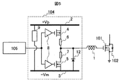
図5は、本実施例にかかるゲート駆動回路の構成図を示す。ゲート駆動回路104の出力部、すなわちオン側ゲート抵抗6とオフ側ゲート抵抗7の接続点にダイオード12のカソードが接続されている。ダイオード12のアノードは、ゲート駆動回路の負側電源3に接続されている。その他の接続様態は、実施例1と同じである。
FIG. 5 is a configuration diagram of the gate drive circuit according to the present embodiment. The cathode of the
ダイオード12を設けることにより、半導体素子101のゲート端子の電位が沈み込んだ時にゲート駆動回路104の出力部がゲート駆動回路の負側電源3に低インピーダンスで接続されるため、ゲート電圧の変動(沈み込み)を抑制できる。
By providing the
図6は、ゲート電圧の沈み込み現象の説明図である。図6に示すように、対アーム側の半導体素子がターンオフする際、半導体素子101はオフ状態であり、並列接続されている還流ダイオード102がフォワードリカバリー動作をする。この時、半導体素子101のドレイン‐ソース間電圧が減少するため、dv/dt<0であるから、ゲート駆動回路104から半導体素子101に向かって変異電流(Cgd*dv/dt)が流れる。
FIG. 6 is an explanatory diagram of the phenomenon of gate voltage sinking. As shown in FIG. 6, when the semiconductor element on the opposite arm side is turned off, the
この変異電流は、ゲート駆動回路の負側電源3、ダイオード12、ゲート配線1を経由して半導体素子101に流れ込む。このとき、図6に示すように、電流経路上の回路インピーダンスに応じて半導体素子101のゲート端子とゲート駆動回路の負側電源3との間に電位差が生じ、半導体素子101のVgsはゲート駆動回路の負側電源3の電圧(−Vm)よりも低く沈み込む。すなわち、(式2)で表されるようにV1+V3の電位差が生じる。ここで、V3はダイオード12の導通に起因した電位差であり、ダイオード12の順方向電圧に等しい。
Vgs=−Vm−(V1+V3) (式2)
This variation current flows into the
Vgs = −Vm− (V1 + V3) (Formula 2)
ゲート電圧の沈み込み現象により、半導体素子101のVgsがその定格電圧の下限値(たとえば−20V)を下回るとゲート酸化膜の信頼性低下が懸念されるが、本実施例では、沈み込み時に電流がダイオード12を経由することにより、ゲート駆動回路の負側電源3からの電圧降下(V1+V3)を抑制でき、ゲート酸化膜の信頼性を確保できる。したがって、ダイオード12の候補としては、順方向電圧(V3)の小さいショットキーバリアダイオードなど望ましいが、ツェナーダイオードやPNダイオードでも良い。
If the Vgs of the
また、(式1)(式2)より、ゲート電圧の変動量(持ち上がり、沈み込み)を抑制するためには、ゲート配線1で発生する電位差(V1)を低減することも有効であり、ゲート配線1の寄生インダクタンス(Lg)を低減することが望ましい。Lgを低減する手法としては、ゲート配線長を最小化する手法や、ゲート電流による磁場が効果的に打ち消しあうようにラミネートブスバー構造等を適用する手法がある。
From (Equation 1) and (Equation 2), it is also effective to reduce the potential difference (V1) generated in the
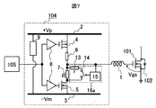
図7は、本実施例にかかるゲート駆動回路の構成図を示す。ゲート電位をゲート駆動回路の負側電源に接続する手段として、実施例2では、ダイオード12を用いたが、本実施例では、低インピーダンス化回路16aを用いている点が異なる。以下、実施例1乃至2との相違点を中心に説明する。
FIG. 7 shows a configuration diagram of the gate drive circuit according to the present embodiment. As a means for connecting the gate potential to the negative power source of the gate drive circuit, the
低インピーダンス化回路16aは、並列化抵抗13、アナログスイッチ14、およびゲートオフ判定部15から構成される。並列化抵抗13は、アナログスイッチ14を介してオフ側ゲート抵抗7に並列に接続される。ゲートオフ判定部15は、ゲート駆動回路104の出力部とアナログスイッチ14の間に接続される。
The
ゲートオフ判定部15は、半導体素子101のゲート‐ソース間電圧(Vgs)をモニタしており、半導体素子101がオフ状態であることをVgsの値から判定する。ゲートオフ判定部15は、半導体素子101がオフ状態であることを判定すると、アナログスイッチ14が閉じられ、オフ側ゲート抵抗7(抵抗値R)と並列化抵抗13(抵抗値r)が並列接続される。並列接続時の抵抗は、RからR/(1+R/r)(<R)に減少する。したがって、半導体素子101のオフ中に、ゲートの電位が沈み込んだ時にゲート駆動回路104の出力部がゲート駆動回路の負側電源3に低インピーダンスで接続されるため、ゲート電圧の変動(沈み込み)を抑制できる。
The gate-off
実施例2では、ダイオード12の整流作用から、ゲートが沈み込むときのみ変動抑制効果があるのに対し、本実施例では、低インピーダンス化回路16aの双方向性から、ゲートの沈み込みと持ち上がりの両方に変動抑制効果がある点で優位である。ゲート電圧の持ち上がり量の抑制により、半導体素子101のオフ時において、半導体素子101のゲート-ソース間電圧が閾値電圧(Vth)まで持ち上がるまでの電位差マージンが大きくなるため、誤オンを防止できる。
In the second embodiment, there is an effect of suppressing the fluctuation only when the gate sinks due to the rectifying action of the
図8は、本実施例にかかるゲート駆動回路の構成図を示す。本実施例では、低インピーダンス化回路として、アナログスイッチでななく、MOSFETを用いている点が異なる。以下、実施例1乃至3との相違点を中心に説明する。 FIG. 8 shows a configuration diagram of the gate drive circuit according to the present embodiment. This embodiment is different in that a MOSFET is used instead of an analog switch as a low impedance circuit. Hereinafter, the difference from the first to third embodiments will be mainly described.
低インピーダンス化回路16bは、電圧クランプ用MOSFET17、およびゲートオフ判定部15から構成される。電圧クランプ用MOS17は、ゲート駆動回路104の出力部とゲート駆動回路の負側電源3の間に接続される。ゲートオフ判定部15は、ゲート駆動回路104の出力部と電圧クランプ用MOS17のゲート端子との間に接続される。
The
ゲートオフ判定部15は、半導体素子101がオフ状態であることを判定すると、電圧クランプ用MOS17をオンさせ、ゲート駆動回路104の出力部とゲート駆動回路の負側電源3とを短絡させる。したがって、半導体素子101のオフ中にゲートの電位が沈み込んだ時に、ゲート駆動回路104の出力部がゲート駆動回路の負側電源3に極めて低インピーダンスで接続されるため、ゲート電圧の変動(沈み込み)を効果的に抑制できる。
When determining that the
本実施例では、ゲート駆動回路104の出力部とゲート駆動回路の負側電源3の間に介在するインピーダンス成分が、電圧クランプ用MOSFET17のオン抵抗のみとなって小さくなるため(たとえば数十mΩ)、実施例3に比べて、より効果的にゲートの変動(沈み込み、持ち上がり)を抑制できる利点がある。
In the present embodiment, the impedance component interposed between the output part of the
1:ゲート配線
2:ゲート駆動回路の正側電源
3:ゲート駆動回路の負側電源
4:P型MOSFET
5:N型MOSFET
6:オン側ゲート抵抗
7:オフ側ゲート抵抗
8:駆動制御装置
9:電源生成部
10:NPNトランジスタ
11:PNPトランジスタ
12:ダイオード
13:並列化抵抗
14:アナログスイッチ
15:ゲートオフ判定部
16a:低インピーダンス化回路
16b:低インピーダンス化回路
17:電圧クランプ用MOSFET
91:定格電圧(上限値)
92:正側電圧電源
93:負側電圧電源
94:定格電圧(下限値)
100:パワーユニット
101:電圧駆動型の半導体素子(IGBT、MOSFETなど)
102:還流ダイオード
103:フィルタコンデンサ
104:ゲート駆動回路
105:指令論理部
106:モータ
107:架線
108:集電装置
109:遮断機
110:フィルタリアクトル
111:車輪
112:レール
1: Gate wiring 2: Positive power supply of gate drive circuit 3: Negative power supply of gate drive circuit 4: P-type MOSFET
5: N-type MOSFET
6: ON-side gate resistance 7: OFF-side gate resistance 8: Drive controller 9: Power supply generation unit 10: NPN transistor 11: PNP transistor 12: Diode 13: Paralleling resistor 14: Analog switch 15: Gate-off
91: Rated voltage (upper limit)
92: Positive side voltage power supply 93: Negative side voltage power supply 94: Rated voltage (lower limit)
100: Power unit 101: Voltage-driven semiconductor element (IGBT, MOSFET, etc.)
102: freewheeling diode 103: filter capacitor 104: gate drive circuit 105: command logic unit 106: motor 107: overhead line 108: current collector 109: circuit breaker 110: filter reactor 111: wheel 112: rail
Claims (17)
前記ゲート駆動回路が、P型MOSFETおよびN側MOSFETが直列に接続され、且つ前記N側MOSFETが負側電源に直接接続されて構成され、前記P型MOSFETと前記N側MOSFETの中間にある出力段が、前記半導体素子のオフ中に負バイアスとなるように前記P型MOSFETおよび前記N型MOSFETを相補的にオンオフすることを特徴とするゲート駆動回路。 In a gate drive circuit for driving a voltage-driven semiconductor element to which SiC is applied,
The gate drive circuit includes a P-type MOSFET and an N-side MOSFET connected in series, and the N-side MOSFET is directly connected to a negative power source, and an output located between the P-type MOSFET and the N-side MOSFET. A gate driving circuit, wherein the stage complementarily turns on and off the P-type MOSFET and the N-type MOSFET so as to be negatively biased while the semiconductor element is off.
前記半導体素子のオフ中に出力段を負バイアスに維持する電圧維持手段を有することを特徴とするゲート駆動回路。 The gate drive circuit according to claim 1,
A gate driving circuit comprising voltage maintaining means for maintaining the output stage at a negative bias while the semiconductor element is off.
前記電圧維持手段が、前記出力部と前記負側電源の間に前記N型MOSFETと並列に接続されたダイオードを含むことを特徴とするゲート駆動回路。 The gate drive circuit according to claim 2,
The gate drive circuit, wherein the voltage maintaining means includes a diode connected in parallel with the N-type MOSFET between the output unit and the negative power source.
前記ダイオードが、ショットキーバリアダイオード、ツェナーダイオード、またはPNダイオードであることを特徴とするゲート駆動回路。 The gate drive circuit according to claim 3.
The gate drive circuit, wherein the diode is a Schottky barrier diode, a Zener diode, or a PN diode.
前記電圧維持手段が、前記出力段とN側MOSFETの中間にあるオフ側ゲート抵抗に並列接続された並列化抵抗と、前記並列化抵抗に直列接続されたスイッチと、前記半導体素子がオフ状態の場合に前記スイッチをオンとする判定部を含むことを特徴とするゲート駆動回路。 The gate drive circuit according to claim 2,
The voltage maintaining means includes a parallel resistor connected in parallel to an off-side gate resistor located between the output stage and the N-side MOSFET, a switch connected in series to the parallel resistor, and the semiconductor element in an off state. A gate drive circuit comprising: a determination unit that turns on the switch.
前記電圧維持手段が、前記出力段と前記負側電源の間で前記N側MOSFETと並列に接続されたMOSFETと、前記半導体素子がオフ状態の場合に前記MOSFETを短絡させる判定部を含むことを特徴とするゲート駆動回路。 The gate drive circuit according to claim 2,
The voltage maintaining means includes a MOSFET connected in parallel with the N-side MOSFET between the output stage and the negative power source, and a determination unit that short-circuits the MOSFET when the semiconductor element is in an off state. A characteristic gate drive circuit.
前記半導体素子が、ノーマリオフの半導体素子であることを特徴とするゲート駆動回路。 The gate drive circuit according to any one of claims 1 to 6,
A gate driving circuit, wherein the semiconductor element is a normally-off semiconductor element.
前記負側電源の電圧生成に、絶縁型電源トランス、または絶縁側DCDCコンバータが用いられることを特徴とするゲート駆動回路 The gate drive circuit according to any one of claims 1 to 7,
An insulated power transformer or an insulated DCDC converter is used for voltage generation of the negative power supply.
P側MOSFET、および負極電源に直接接続されたN側MOSFETを相補的にオンオフして、直列に接続されている前記P型MOSFETと前記N側MOSFETの中間にある出力段を、前記半導体素子のオフ中に負バイアスとすることを特徴とするゲート駆動方法。 In a gate driving method of a voltage-driven semiconductor element to which SiC is applied,
The P-side MOSFET and the N-side MOSFET directly connected to the negative power supply are complementarily turned on and off, and an output stage intermediate between the P-type MOSFET and the N-side MOSFET connected in series is connected to the semiconductor element. A gate driving method, wherein a negative bias is applied during off.
電圧維持手段により、前記半導体素子のオフ中に出力段を負バイアスに維持することを特徴とするゲート駆動方法。 The gate driving method according to claim 10.
A gate driving method characterized in that the output stage is maintained at a negative bias while the semiconductor element is turned off by voltage maintaining means.
前記電圧維持手段が、前記出力部と前記負側電源の間に前記N型MOSFETと並列に接続されたダイオードを含むことを特徴とするゲート駆動方法。 The gate driving method according to claim 11,
The gate driving method, wherein the voltage maintaining means includes a diode connected in parallel with the N-type MOSFET between the output unit and the negative power source.
前記ダイオードが、ショットキーバリアダイオード、ツェナーダイオード、またはPNダイオードであることを特徴とするゲート駆動方法。 The gate driving method according to claim 12, wherein
The gate driving method, wherein the diode is a Schottky barrier diode, a Zener diode, or a PN diode.
前記半導体素子がオフ状態の場合に、前記出力段とN側MOSFETの中間にあるオフ側ゲート抵抗に並列接続された並列化抵抗に直列接続されたスイッチをオンとすることを特徴とするゲート駆動方法。 The gate driving method according to claim 11,
When the semiconductor element is in an off state, a gate drive is characterized in that a switch connected in series to a paralleled resistor connected in parallel to an off-side gate resistor located between the output stage and the N-side MOSFET is turned on. Method.
前記半導体素子がオフ状態の場合に、前記出力段と前記負側電源の間で前記N側MOSFETと並列に接続されたMOSFETを短絡させることを特徴とするゲート駆動方法。 The gate driving method according to claim 11,
A gate driving method comprising: short-circuiting a MOSFET connected in parallel with the N-side MOSFET between the output stage and the negative power source when the semiconductor element is in an off state.
前記半導体素子が、ノーマリオフの半導体素子であることを特徴とするゲート駆動方法。 The gate drive method according to any one of claims 11 to 15,
A gate driving method, wherein the semiconductor element is a normally-off semiconductor element.
絶縁型電源トランス、または絶縁側DCDCコンバータにより、前記負側電源の電圧を生成することを特徴とするゲート駆動方法。 The gate driving method according to any one of claims 11 to 16,
A gate driving method, wherein the voltage of the negative power source is generated by an insulating power transformer or an insulating DCDC converter.
Priority Applications (4)
| Application Number | Priority Date | Filing Date | Title |
|---|---|---|---|
| JP2018082704A JP2019193406A (en) | 2018-04-24 | 2018-04-24 | Gate drive circuit and gate drive method |
| CN201980025569.4A CN111971884A (en) | 2018-04-24 | 2019-03-11 | Gate driving circuit and gate driving method |
| PCT/JP2019/009651 WO2019207977A1 (en) | 2018-04-24 | 2019-03-11 | Gate drive circuit and gate drive method |
| EP19792293.3A EP3787164A1 (en) | 2018-04-24 | 2019-03-11 | Gate drive circuit and gate drive method |
Applications Claiming Priority (1)
| Application Number | Priority Date | Filing Date | Title |
|---|---|---|---|
| JP2018082704A JP2019193406A (en) | 2018-04-24 | 2018-04-24 | Gate drive circuit and gate drive method |
Publications (2)
| Publication Number | Publication Date |
|---|---|
| JP2019193406A true JP2019193406A (en) | 2019-10-31 |
| JP2019193406A5 JP2019193406A5 (en) | 2021-01-28 |
Family
ID=68295092
Family Applications (1)
| Application Number | Title | Priority Date | Filing Date |
|---|---|---|---|
| JP2018082704A Pending JP2019193406A (en) | 2018-04-24 | 2018-04-24 | Gate drive circuit and gate drive method |
Country Status (4)
| Country | Link |
|---|---|
| EP (1) | EP3787164A1 (en) |
| JP (1) | JP2019193406A (en) |
| CN (1) | CN111971884A (en) |
| WO (1) | WO2019207977A1 (en) |
Cited By (1)
| Publication number | Priority date | Publication date | Assignee | Title |
|---|---|---|---|---|
| CN114884320A (en) * | 2022-07-07 | 2022-08-09 | 深圳平创半导体有限公司 | Device for reducing power consumption of grid negative pressure driving circuit |
Families Citing this family (2)
| Publication number | Priority date | Publication date | Assignee | Title |
|---|---|---|---|---|
| CN115632539A (en) | 2021-07-01 | 2023-01-20 | 纳维达斯半导体有限公司 | Integrated power device with energy harvesting gate driver |
| EP4131779A1 (en) | 2021-08-03 | 2023-02-08 | Infineon Technologies Austria AG | Gate driver device |
Citations (7)
| Publication number | Priority date | Publication date | Assignee | Title |
|---|---|---|---|---|
| JP2009055696A (en) * | 2007-08-27 | 2009-03-12 | Fuji Electric Device Technology Co Ltd | Gate drive circuit of semiconductor device and gate drive method |
| JP2012199763A (en) * | 2011-03-22 | 2012-10-18 | Sanken Electric Co Ltd | Gate drive circuit |
| JP2015023774A (en) * | 2013-07-23 | 2015-02-02 | 日新電機株式会社 | Gate drive circuit |
| WO2015182658A1 (en) * | 2014-05-30 | 2015-12-03 | 三菱電機株式会社 | Circuit for driving electrical-power semiconductor element |
| JP2016034178A (en) * | 2014-07-31 | 2016-03-10 | 株式会社日立製作所 | Power conversion apparatus and control method of the same |
| JP2016123199A (en) * | 2014-12-25 | 2016-07-07 | パナソニックIpマネジメント株式会社 | Driving device and power conversion device |
| WO2018008398A1 (en) * | 2016-07-04 | 2018-01-11 | 三菱電機株式会社 | Drive circuit and power module using same |
Family Cites Families (6)
| Publication number | Priority date | Publication date | Assignee | Title |
|---|---|---|---|---|
| JP2009225506A (en) * | 2008-03-13 | 2009-10-01 | Toshiba Corp | Power converter |
| JP5130310B2 (en) * | 2010-03-17 | 2013-01-30 | 日立アプライアンス株式会社 | GATE DRIVING CIRCUIT AND POWER CONVERSION DEVICE FOR VOLTAGE-DRIVEN SEMICONDUCTOR ELEMENT |
| JP5503427B2 (en) | 2010-06-22 | 2014-05-28 | 本田技研工業株式会社 | Gate drive circuit |
| JP5975833B2 (en) * | 2012-02-01 | 2016-08-23 | 三菱電機株式会社 | Power converter |
| JP2014057491A (en) * | 2012-09-14 | 2014-03-27 | Mitsubishi Electric Corp | Gate drive circuit for semiconductor switching element |
| JP6798179B2 (en) * | 2016-07-29 | 2020-12-09 | 富士電機株式会社 | 3-level chopper device |
-
2018
- 2018-04-24 JP JP2018082704A patent/JP2019193406A/en active Pending
-
2019
- 2019-03-11 CN CN201980025569.4A patent/CN111971884A/en active Pending
- 2019-03-11 EP EP19792293.3A patent/EP3787164A1/en not_active Withdrawn
- 2019-03-11 WO PCT/JP2019/009651 patent/WO2019207977A1/en unknown
Patent Citations (7)
| Publication number | Priority date | Publication date | Assignee | Title |
|---|---|---|---|---|
| JP2009055696A (en) * | 2007-08-27 | 2009-03-12 | Fuji Electric Device Technology Co Ltd | Gate drive circuit of semiconductor device and gate drive method |
| JP2012199763A (en) * | 2011-03-22 | 2012-10-18 | Sanken Electric Co Ltd | Gate drive circuit |
| JP2015023774A (en) * | 2013-07-23 | 2015-02-02 | 日新電機株式会社 | Gate drive circuit |
| WO2015182658A1 (en) * | 2014-05-30 | 2015-12-03 | 三菱電機株式会社 | Circuit for driving electrical-power semiconductor element |
| JP2016034178A (en) * | 2014-07-31 | 2016-03-10 | 株式会社日立製作所 | Power conversion apparatus and control method of the same |
| JP2016123199A (en) * | 2014-12-25 | 2016-07-07 | パナソニックIpマネジメント株式会社 | Driving device and power conversion device |
| WO2018008398A1 (en) * | 2016-07-04 | 2018-01-11 | 三菱電機株式会社 | Drive circuit and power module using same |
Cited By (1)
| Publication number | Priority date | Publication date | Assignee | Title |
|---|---|---|---|---|
| CN114884320A (en) * | 2022-07-07 | 2022-08-09 | 深圳平创半导体有限公司 | Device for reducing power consumption of grid negative pressure driving circuit |
Also Published As
| Publication number | Publication date |
|---|---|
| WO2019207977A1 (en) | 2019-10-31 |
| CN111971884A (en) | 2020-11-20 |
| EP3787164A1 (en) | 2021-03-03 |
Similar Documents
| Publication | Publication Date | Title |
|---|---|---|
| JP6619381B2 (en) | Method and circuit for operating a circuit | |
| EP3035532B1 (en) | Gate drive circuit and method of operating same | |
| US9444448B2 (en) | High performance IGBT gate drive | |
| US9362903B2 (en) | Gate drivers for circuits based on semiconductor devices | |
| US20170324316A1 (en) | Semiconductor device | |
| CN103986359B (en) | Power inverter | |
| US20110121884A1 (en) | Half-bridge circuits employing normally on switches and methods of preventing unintended current flow therein | |
| US20130271187A1 (en) | Driver for semiconductor switch element | |
| US20160285386A1 (en) | Rectifier | |
| WO2013115000A1 (en) | Drive circuit for semiconductor switching element and power conversion circuit using same | |
| WO2019207977A1 (en) | Gate drive circuit and gate drive method | |
| JP2009011013A (en) | Power conversion equipment | |
| WO2016030954A1 (en) | Driving circuit, power conversion device, and motor system | |
| JP5382535B2 (en) | Power supply device for gate drive circuit | |
| JP6122542B1 (en) | Active clamp circuit | |
| JP2019041499A (en) | Driver circuit and semiconductor module | |
| JP6004988B2 (en) | Gate control device for power semiconductor device | |
| CN110741546B (en) | Rectifier circuit and power supply device | |
| JP2019041514A (en) | Driving circuit of semiconductor element | |
| JPH10209832A (en) | Semiconductor switch circuit | |
| US11271547B2 (en) | Gate drive circuit, drive device, semiconductor device, and gate drive method | |
| WO2024057598A1 (en) | Gate drive circuit for semiconductor switching element, electric motor control system, and semiconductor device | |
| US11909384B2 (en) | Direct-drive D-mode GaN half-bridge power module | |
| JP6679967B2 (en) | Driving device for semiconductor element | |
| JP2021185741A (en) | Power conversion device |
Legal Events
| Date | Code | Title | Description |
|---|---|---|---|
| A521 | Request for written amendment filed |
Free format text: JAPANESE INTERMEDIATE CODE: A523 Effective date: 20201211 |
|
| A621 | Written request for application examination |
Free format text: JAPANESE INTERMEDIATE CODE: A621 Effective date: 20201211 |
|
| A871 | Explanation of circumstances concerning accelerated examination |
Free format text: JAPANESE INTERMEDIATE CODE: A871 Effective date: 20201211 |
|
| A975 | Report on accelerated examination |
Free format text: JAPANESE INTERMEDIATE CODE: A971005 Effective date: 20201221 |
|
| A131 | Notification of reasons for refusal |
Free format text: JAPANESE INTERMEDIATE CODE: A131 Effective date: 20201228 |
|
| A521 | Request for written amendment filed |
Free format text: JAPANESE INTERMEDIATE CODE: A523 Effective date: 20210226 |
|
| A02 | Decision of refusal |
Free format text: JAPANESE INTERMEDIATE CODE: A02 Effective date: 20210427 |