JP2018190875A - Semiconductor device - Google Patents
Semiconductor device Download PDFInfo
- Publication number
- JP2018190875A JP2018190875A JP2017093698A JP2017093698A JP2018190875A JP 2018190875 A JP2018190875 A JP 2018190875A JP 2017093698 A JP2017093698 A JP 2017093698A JP 2017093698 A JP2017093698 A JP 2017093698A JP 2018190875 A JP2018190875 A JP 2018190875A
- Authority
- JP
- Japan
- Prior art keywords
- pad
- terminal
- semiconductor device
- back surface
- resin
- Prior art date
- Legal status (The legal status is an assumption and is not a legal conclusion. Google has not performed a legal analysis and makes no representation as to the accuracy of the status listed.)
- Granted
Links
Images


Classifications
-
- H—ELECTRICITY
- H01—ELECTRIC ELEMENTS
- H01L—SEMICONDUCTOR DEVICES NOT COVERED BY CLASS H10
- H01L2224/00—Indexing scheme for arrangements for connecting or disconnecting semiconductor or solid-state bodies and methods related thereto as covered by H01L24/00
- H01L2224/01—Means for bonding being attached to, or being formed on, the surface to be connected, e.g. chip-to-package, die-attach, "first-level" interconnects; Manufacturing methods related thereto
- H01L2224/02—Bonding areas; Manufacturing methods related thereto
- H01L2224/04—Structure, shape, material or disposition of the bonding areas prior to the connecting process
- H01L2224/05—Structure, shape, material or disposition of the bonding areas prior to the connecting process of an individual bonding area
- H01L2224/0554—External layer
- H01L2224/0555—Shape
- H01L2224/05552—Shape in top view
- H01L2224/05554—Shape in top view being square
-
- H—ELECTRICITY
- H01—ELECTRIC ELEMENTS
- H01L—SEMICONDUCTOR DEVICES NOT COVERED BY CLASS H10
- H01L2224/00—Indexing scheme for arrangements for connecting or disconnecting semiconductor or solid-state bodies and methods related thereto as covered by H01L24/00
- H01L2224/01—Means for bonding being attached to, or being formed on, the surface to be connected, e.g. chip-to-package, die-attach, "first-level" interconnects; Manufacturing methods related thereto
- H01L2224/26—Layer connectors, e.g. plate connectors, solder or adhesive layers; Manufacturing methods related thereto
- H01L2224/31—Structure, shape, material or disposition of the layer connectors after the connecting process
- H01L2224/32—Structure, shape, material or disposition of the layer connectors after the connecting process of an individual layer connector
- H01L2224/321—Disposition
- H01L2224/32151—Disposition the layer connector connecting between a semiconductor or solid-state body and an item not being a semiconductor or solid-state body, e.g. chip-to-substrate, chip-to-passive
- H01L2224/32221—Disposition the layer connector connecting between a semiconductor or solid-state body and an item not being a semiconductor or solid-state body, e.g. chip-to-substrate, chip-to-passive the body and the item being stacked
- H01L2224/32245—Disposition the layer connector connecting between a semiconductor or solid-state body and an item not being a semiconductor or solid-state body, e.g. chip-to-substrate, chip-to-passive the body and the item being stacked the item being metallic
-
- H—ELECTRICITY
- H01—ELECTRIC ELEMENTS
- H01L—SEMICONDUCTOR DEVICES NOT COVERED BY CLASS H10
- H01L2224/00—Indexing scheme for arrangements for connecting or disconnecting semiconductor or solid-state bodies and methods related thereto as covered by H01L24/00
- H01L2224/01—Means for bonding being attached to, or being formed on, the surface to be connected, e.g. chip-to-package, die-attach, "first-level" interconnects; Manufacturing methods related thereto
- H01L2224/42—Wire connectors; Manufacturing methods related thereto
- H01L2224/47—Structure, shape, material or disposition of the wire connectors after the connecting process
- H01L2224/48—Structure, shape, material or disposition of the wire connectors after the connecting process of an individual wire connector
- H01L2224/4805—Shape
- H01L2224/4809—Loop shape
- H01L2224/48091—Arched
-
- H—ELECTRICITY
- H01—ELECTRIC ELEMENTS
- H01L—SEMICONDUCTOR DEVICES NOT COVERED BY CLASS H10
- H01L2224/00—Indexing scheme for arrangements for connecting or disconnecting semiconductor or solid-state bodies and methods related thereto as covered by H01L24/00
- H01L2224/01—Means for bonding being attached to, or being formed on, the surface to be connected, e.g. chip-to-package, die-attach, "first-level" interconnects; Manufacturing methods related thereto
- H01L2224/42—Wire connectors; Manufacturing methods related thereto
- H01L2224/47—Structure, shape, material or disposition of the wire connectors after the connecting process
- H01L2224/48—Structure, shape, material or disposition of the wire connectors after the connecting process of an individual wire connector
- H01L2224/481—Disposition
- H01L2224/48151—Connecting between a semiconductor or solid-state body and an item not being a semiconductor or solid-state body, e.g. chip-to-substrate, chip-to-passive
- H01L2224/48221—Connecting between a semiconductor or solid-state body and an item not being a semiconductor or solid-state body, e.g. chip-to-substrate, chip-to-passive the body and the item being stacked
- H01L2224/48245—Connecting between a semiconductor or solid-state body and an item not being a semiconductor or solid-state body, e.g. chip-to-substrate, chip-to-passive the body and the item being stacked the item being metallic
- H01L2224/48247—Connecting between a semiconductor or solid-state body and an item not being a semiconductor or solid-state body, e.g. chip-to-substrate, chip-to-passive the body and the item being stacked the item being metallic connecting the wire to a bond pad of the item
-
- H—ELECTRICITY
- H01—ELECTRIC ELEMENTS
- H01L—SEMICONDUCTOR DEVICES NOT COVERED BY CLASS H10
- H01L2224/00—Indexing scheme for arrangements for connecting or disconnecting semiconductor or solid-state bodies and methods related thereto as covered by H01L24/00
- H01L2224/01—Means for bonding being attached to, or being formed on, the surface to be connected, e.g. chip-to-package, die-attach, "first-level" interconnects; Manufacturing methods related thereto
- H01L2224/42—Wire connectors; Manufacturing methods related thereto
- H01L2224/47—Structure, shape, material or disposition of the wire connectors after the connecting process
- H01L2224/49—Structure, shape, material or disposition of the wire connectors after the connecting process of a plurality of wire connectors
- H01L2224/491—Disposition
- H01L2224/4911—Disposition the connectors being bonded to at least one common bonding area, e.g. daisy chain
- H01L2224/49113—Disposition the connectors being bonded to at least one common bonding area, e.g. daisy chain the connectors connecting different bonding areas on the semiconductor or solid-state body to a common bonding area outside the body, e.g. converging wires
-
- H—ELECTRICITY
- H01—ELECTRIC ELEMENTS
- H01L—SEMICONDUCTOR DEVICES NOT COVERED BY CLASS H10
- H01L2224/00—Indexing scheme for arrangements for connecting or disconnecting semiconductor or solid-state bodies and methods related thereto as covered by H01L24/00
- H01L2224/73—Means for bonding being of different types provided for in two or more of groups H01L2224/10, H01L2224/18, H01L2224/26, H01L2224/34, H01L2224/42, H01L2224/50, H01L2224/63, H01L2224/71
- H01L2224/732—Location after the connecting process
- H01L2224/73251—Location after the connecting process on different surfaces
- H01L2224/73265—Layer and wire connectors
-
- H—ELECTRICITY
- H01—ELECTRIC ELEMENTS
- H01L—SEMICONDUCTOR DEVICES NOT COVERED BY CLASS H10
- H01L2924/00—Indexing scheme for arrangements or methods for connecting or disconnecting semiconductor or solid-state bodies as covered by H01L24/00
- H01L2924/15—Details of package parts other than the semiconductor or other solid state devices to be connected
- H01L2924/181—Encapsulation
Landscapes
- Lead Frames For Integrated Circuits (AREA)
Abstract
Description
本発明は、パッケージ形式がQFNである半導体装置に関する。 The present invention relates to a semiconductor device whose package format is QFN.
複数の端子(リード)の基となるリードフレームの一部であるダイパッドに半導体素子を搭載し、これらを封止樹脂で覆った半導体装置には、様々な種類のパッケージ形式が存在する。これらのパッケージ形式のうち、QFN(Quad Flat No-leads)は、封止樹脂から複数の端子が側方に全く突出しない形式である。QFNは、回路基板に対する実装範囲を縮小することができるため、電子機器の小型化に寄与する。 There are various types of package formats for semiconductor devices in which semiconductor elements are mounted on a die pad, which is a part of a lead frame that is a base of a plurality of terminals (leads), and these are covered with a sealing resin. Among these package types, QFN (Quad Flat No-leads) is a type in which a plurality of terminals do not protrude sideways at all from the sealing resin. Since QFN can reduce the mounting range on the circuit board, it contributes to downsizing of electronic devices.
特許文献1には、パッケージ形式がQFNである半導体装置の一例が開示されている。当該半導体装置は、半導体素子(半導体チップ)が搭載されるダイパッドと、ダイパッドの周囲に配置された複数の端子(リード)と、これらを覆う封止樹脂(封止体)とを備える。当該半導体装置では、ダイパッドの裏面が封止樹脂から露出し、かつ平面視におけるダイパッドの面積が装置面積の大半を占める構成となっている。このため、当該半導体装置では、半導体素子から発生した熱をダイパッドから効率よく外部に放出することができる。ただし、ダイパッドの体積が比較的大きいため、当該半導体装置の使用にかかる温度サイクルなどによってダイパッドに熱膨張が生じる。そして、当該熱膨張に起因した熱応力が封止樹脂に作用する。封止樹脂に作用する熱応力の集中が顕著になると、封止樹脂に亀裂が発生するおそれがある。当該亀裂に水分などが進入すると、当該半導体装置に不具合が発生することが懸念される。こうした理由から、封止樹脂に作用する熱応力の集中を緩和するためダイパッドの大きさを縮小させた場合、封止樹脂から露出するダイパッドの表面積が減少する。この場合においては、半導体素子から発生した熱にかかる放熱性の低下が課題となる。
本発明は上記事情に鑑み、封止樹脂に作用する熱応力の集中を緩和しつつ、放熱性を確保することが可能な半導体装置を提供することをその課題とする。 In view of the above circumstances, an object of the present invention is to provide a semiconductor device capable of ensuring heat dissipation while relaxing the concentration of thermal stress acting on the sealing resin.
本発明によって提供される半導体装置は、厚さ方向において互いに反対側を向く搭載面およびパッド裏面を有するダイパッドと、前記搭載面に搭載された半導体素子と各々が前記パッド裏面と同方向を向く端子裏面を有するとともに、前記ダイパッドの厚さ方向視において前記ダイパッドを囲むように配置され、かつ前記半導体素子に導通する複数の端子と、前記パッド裏面と同方向を向く樹脂裏面を有し、かつ前記半導体素子と、前記ダイパッドおよび複数の前記端子のそれぞれ一部ずつとを覆う封止樹脂と、を備える半導体装置であって、前記パッド裏面および前記端子裏面は、ともに前記樹脂裏面から露出し、前記ダイパッドには、前記パッド裏面から凹むパッド凹部が形成されていることを特徴としている。 A semiconductor device provided by the present invention includes a die pad having a mounting surface and a pad back surface facing in opposite directions in the thickness direction, a semiconductor element mounted on the mounting surface, and a terminal each facing in the same direction as the pad back surface A plurality of terminals that are disposed so as to surround the die pad as viewed in the thickness direction of the die pad and that are electrically connected to the semiconductor element; and a resin back surface that faces in the same direction as the pad back surface, and A semiconductor device comprising a semiconductor element and a sealing resin that covers each of the die pad and each of the plurality of terminals, wherein the pad back surface and the terminal back surface are both exposed from the resin back surface, The die pad is characterized in that a pad recess recessed from the back surface of the pad is formed.
本発明の実施において好ましくは、前記パッド凹部は、前記樹脂裏面から露出している。 In the practice of the present invention, the pad recess is preferably exposed from the resin back surface.
本発明の実施において好ましくは、前記パッド凹部は、前記パッド裏面の中央を囲む複数の環状溝から構成され、前記パッド裏面において各々の前記環状溝によって囲まれた領域の中心位置は、いずれも同一である。 Preferably, in the implementation of the present invention, the pad recess is composed of a plurality of annular grooves surrounding the center of the back surface of the pad, and the center positions of the regions surrounded by the annular grooves on the pad back surface are all the same. It is.
本発明の実施において好ましくは、前記パッド凹部は、前記厚さ方向に対して直角である方向に沿って延びる複数の溝から構成される。 In the practice of the present invention, the pad recess is preferably composed of a plurality of grooves extending along a direction perpendicular to the thickness direction.
本発明の実施において好ましくは、前記ダイパッドは、前記パッド裏面に交差し、かつ複数の前記端子に対向するパッド側面をさらに有し、前記ダイパッドには、前記搭載面と面一であり、かつ前記パッド側面から複数の前記端子に向けて突出するパッド突出部が形成されている。 Preferably, in the embodiment of the present invention, the die pad further includes a pad side surface that intersects the pad back surface and faces the plurality of terminals, the die pad being flush with the mounting surface, and the Pad protrusions that protrude from the side surface of the pad toward the plurality of terminals are formed.
本発明の実施において好ましくは、前記パッド凹部には、前記封止樹脂が充填され、前記パッド裏面は、パッド中央部と、前記パッド中央部の周囲に位置するパッド外周部と、を有し、前記パッド中央部および前記パッド外周部は、前記厚さ方向視において前記パッド凹部により互いに隔てられている。 Preferably, in the implementation of the present invention, the pad recess is filled with the sealing resin, and the back surface of the pad has a pad center part and a pad outer peripheral part located around the pad center part, The pad center portion and the pad outer peripheral portion are separated from each other by the pad recess when viewed in the thickness direction.
本発明の実施において好ましくは、前記パッド外周部は、前記厚さ方向に対して直角である一方向において互いに離間した一対の第1領域を有する。 In an embodiment of the present invention, preferably, the pad outer peripheral portion has a pair of first regions separated from each other in one direction perpendicular to the thickness direction.
本発明の実施において好ましくは、前記パッド外周部は、前記厚さ方向および前記一方向の双方に対して直角である方向において互いに離間した一対の第2領域を有する。 In the practice of the present invention, preferably, the pad outer peripheral portion has a pair of second regions spaced from each other in a direction perpendicular to both the thickness direction and the one direction.
本発明の実施において好ましくは、前記搭載面の端縁には、前記厚さ方向視において前記搭載面の四隅から前記ダイパッドの内側に向かって凹む搭載面凹部が形成され、前記厚さ方向視において前記半導体素子の一部が前記搭載面凹部に重なっている。 Preferably, in the implementation of the present invention, a mounting surface recess that is recessed from the four corners of the mounting surface toward the inside of the die pad in the thickness direction view is formed at an edge of the mounting surface, and in the thickness direction view. A part of the semiconductor element overlaps the mounting surface recess.
本発明の実施において好ましくは、前記厚さ方向視において前記半導体素子の一部が前記パッド外周部に重なっている。 In the implementation of the present invention, preferably, a part of the semiconductor element overlaps the outer peripheral portion of the pad in the thickness direction view.
本発明の実施において好ましくは、前記厚さ方向において、前記パッド外周部の位置は、前記パッド中央部の位置に等しい。 In the embodiment of the present invention, preferably, in the thickness direction, the position of the pad outer peripheral portion is equal to the position of the pad central portion.
本発明の実施において好ましくは、前記端子は、前記搭載面と同方向を向く端子主面をさらに有し、前記半導体素子と前記端子主面とを接続するワイヤをさらに備える。 In the embodiment of the present invention, preferably, the terminal further includes a terminal main surface facing the same direction as the mounting surface, and further includes a wire connecting the semiconductor element and the terminal main surface.
本発明の実施において好ましくは、前記ダイパッドおよび前記端子には、前記搭載面および前記端子主面のいずれか一方に接する内装めっき層が設けられている。 In the embodiment of the present invention, preferably, the die pad and the terminal are provided with an interior plating layer in contact with either the mounting surface or the terminal main surface.
本発明の実施において好ましくは、前記端子は、前記端子主面および前記端子裏面の双方に交差し、かつ外側を向く端子外側面をさらに有し、前記封止樹脂は、前記樹脂裏面に交差する樹脂側面をさらに有し、前記端子外側面は、前記樹脂側面から露出している。 Preferably, in the embodiment of the present invention, the terminal further includes a terminal outer surface that intersects both the terminal main surface and the terminal back surface and faces outward, and the sealing resin intersects the resin back surface. It further has a resin side surface, and the terminal outer surface is exposed from the resin side surface.
本発明の実施において好ましくは、前記端子は、前記端子裏面に交差し、かつ前記端子外側面とは反対側を向く端子内側面をさらに有し、前記端子には、前記端子主面と面一であり、かつ前記端子内側面から前記ダイパッドに向けて突出する端子突出部が形成されている。 Preferably, in the implementation of the present invention, the terminal further includes a terminal inner surface that intersects the terminal back surface and faces away from the terminal outer surface, and the terminal is flush with the terminal main surface. And a terminal protrusion that protrudes from the inner surface of the terminal toward the die pad.
本発明の実施において好ましくは、複数の前記端子は、前記厚さ方向に対して直角である第1方向に沿って配列された複数の第1端子と、前記厚さ方向および前記第1方向の双方に対して直角である第2方向に沿って配列された複数の第2端子と、を含み、前記端子外側面は、前記樹脂側面と面一である。 Preferably, in the implementation of the present invention, the plurality of terminals include a plurality of first terminals arranged along a first direction perpendicular to the thickness direction, and the thickness direction and the first direction. A plurality of second terminals arranged along a second direction that is perpendicular to both, and the terminal outer surface is flush with the resin side surface.
本発明にかかる半導体装置によれば、封止樹脂に作用する熱応力の集中を緩和しつつ、放熱性を確保することが可能となる。 According to the semiconductor device of the present invention, it is possible to ensure heat dissipation while reducing the concentration of thermal stress acting on the sealing resin.
本発明のその他の特徴および利点は、添付図面に基づき以下に行う詳細な説明によって、より明らかとなろう。 Other features and advantages of the present invention will become more apparent from the detailed description given below with reference to the accompanying drawings.
本発明を実施するための形態(以下「実施形態」という。)について、添付図面に基づいて説明する。 A mode for carrying out the present invention (hereinafter referred to as “embodiment”) will be described with reference to the accompanying drawings.
〔第1実施形態〕
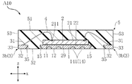
図1〜図11に基づき、本発明の第1実施形態にかかる半導体装置A10について説明する。半導体装置A10は、ダイパッド1、半導体素子2、複数の端子3および封止樹脂5を備える。本実施形態では、半導体装置A10は、ワイヤ4をさらに備える。
[First Embodiment]
A semiconductor device A10 according to the first embodiment of the present invention will be described with reference to FIGS. The semiconductor device A10 includes a
図3は、理解の便宜上、封止樹脂5を透過している。図3において透過した封止樹脂5を想像線(二点鎖線)で示している。図8は、図6に示す端子3付近を拡大している。図9は、図6に示すダイパッド1付近を拡大している。
In FIG. 3, the sealing
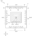
半導体装置A10は、様々な電子機器の回路基板に表面実装される。半導体装置A10は、パッケージ形式がQFNである。図1などに示すように、ダイパッド1の厚さ方向z視(以下「平面視」と呼ぶ。)における半導体装置A10は、矩形状である。ここで、説明の便宜上、ダイパッド1の厚さ方向z(以下、単に「厚さ方向z」と呼ぶ。)に対して直角である方向(図2における横方向)を第1方向xと呼ぶ。また、ダイパッド1の厚さ方向zおよび第1方向xの双方に対して直角である方向(図2における縦方向)を第2方向yと呼ぶ。
The semiconductor device A10 is surface-mounted on circuit boards of various electronic devices. The semiconductor device A10 has a QFN package format. As shown in FIG. 1 and the like, the semiconductor device A10 in the thickness direction z view of the die pad 1 (hereinafter referred to as “plan view”) has a rectangular shape. Here, for convenience of explanation, a direction (lateral direction in FIG. 2) perpendicular to the thickness direction z of the die pad 1 (hereinafter simply referred to as “thickness direction z”) is referred to as a first direction x. A direction (vertical direction in FIG. 2) perpendicular to both the thickness direction z and the first direction x of the
ダイパッド1は、図3および図6に示すように、半導体素子2が搭載される部材である。ダイパッド1は、金属材料から構成され、当該金属材料は、たとえばCuである。ダイパッド1は、当該金属材料を加工したリードフレームをその由来としている。ダイパッド1は、搭載面11、パッド裏面12、パッド側面13およびパッド斜材16を有する。
As shown in FIGS. 3 and 6, the
図6および図9に示すように、搭載面11は、厚さ方向zを向く。図3に示すように、搭載面11は、矩形状である。搭載面11に半導体素子2が搭載されている。搭載面11において、半導体素子2が搭載されない部分は、封止樹脂5に覆われている。
As shown in FIGS. 6 and 9, the mounting
図6および図9に示すように、パッド裏面12は、厚さ方向zにおいて搭載面11とは反対側を向く。図2に示すように、パッド裏面12は、矩形状であり、その面積は搭載面11よりも小に設定されている。本実施形態では、パッド裏面12は、封止樹脂5から露出している。
As shown in FIGS. 6 and 9, the pad back
図3および図9に示すように、パッド側面13は、パッド裏面12に交差し、かつ複数の端子3に対向している。パッド側面13は、4つの面から構成されており、各々のパッド側面13は、第1方向xおよび第2方向yのいずれか一方を向く。厚さ方向zにおいて、搭載面11とパッド裏面12との間に位置するパッド側面13の上端は、第1方向xおよび第2方向yのいずれか一方に向けて屈曲している。パッド側面13は、封止樹脂5に覆われている。
As shown in FIGS. 3 and 9, the
図2、図6および図9に示すように、ダイパッド1には、パッド裏面12から凹むパッド凹部14が形成されている。本実施形態では、パッド凹部14は、パッド裏面12とともに封止樹脂5から露出している。また、本実施形態では、パッド凹部14は、パッド裏面12から凹み、かつパッド裏面12の中央を囲む複数の環状溝141から構成される。図2に示すように、パッド裏面12において各々の環状溝141によって囲まれた領域の中心位置Cは、いずれも同一である。本実施形態では、各々の環状溝141によって囲まれた領域がいずれも矩形であり、中心位置Cは、当該領域の対角線の交点を指す。ここで、パッド裏面12の中央は、中心位置Cと同一である。なお、各々の環状溝141によって囲まれた領域は、たとえば円形であってもよい。パッド凹部14は、たとえばエッチングによりダイパッド1に形成することができる。
As shown in FIGS. 2, 6, and 9, a
図10および図11は、半導体装置A10の変形例である半導体装置A11を示している。パッド凹部14は、半導体装置A10のような複数の環状溝141以外に、本変形例のように複数の溝142から構成される形態であってもよい。各々の溝142は、厚さ方向zに対して直角である方向に沿って延びている。本変形例では、複数の溝142は、パッド裏面12から凹み、かつ第1方向xに沿って配列されている。各々の溝142は、第2方向yに沿って延びている。なお、複数の溝142は、第2方向yに沿って配列され、かつ各々の溝142が第1方向xに沿って延びる構成であってもよい。また、各々の溝142は、第1方向xおよび第2方向yの双方に対して斜め方向に沿って延びる構成であってもよい。
10 and 11 show a semiconductor device A11 that is a modification of the semiconductor device A10. In addition to the plurality of
図3、図6および図9に示すように、ダイパッド1には、搭載面11と面一であり、かつパッド側面13から複数の端子3に向けて突出する庇状のパッド突出部15が形成されている。パッド突出部15は、ダイパッド1において4箇所形成されており、各々のパッド突出部15は、第1方向xおよび第2方向yのいずれか一方に向けて突出している。パッド突出部15は、パッド端面151およびパッド中間面152を有する。パッド端面151は、厚さ方向zに沿っており、かつ第1方向xおよび第2方向yのいずれか一方を向く。パッド中間面152は、パッド裏面12と同方向を向き、かつパッド端面151に交差している。パッド中間面152は、ダイパッド1の内側においてパッド側面13につながっている。厚さ方向zにおいて、搭載面11からパッド中間面152までの距離は、搭載面11からパッド裏面12までの距離の約半分である。パッド突出部15は、封止樹脂5に覆われている。
As shown in FIGS. 3, 6, and 9, the
図3および図7に示すように、パッド斜材16は、2つのパッド端面151が交差する部分から第1方向xおよび第2方向yの双方に対して斜めに延びている。パッド斜材16は、4本から構成され、かつ平面視においてダイパッド1の四隅から放射状に延びている。パッド斜材16は、斜材上面161、斜材下面162および斜材端面163を有する。斜材上面161は、搭載面11と同方向を向き、かつ搭載面11に面一である。斜材下面162は、パッド裏面12と同方向を向く。パッド斜材16が延びる方向において、斜材下面162の一端は、パッド中間面152につながっている。また、厚さ方向zにおいて、斜材上面161から斜材下面162までの距離は、搭載面11からパッド中間面152までの距離に略等しい。斜材端面163は、パッド斜材16が延びる方向においてパッド斜材16の先端に位置し、かつ斜材上面161および斜材下面162の双方に交差している。斜材端面163は、L形状であり、かつ封止樹脂5から外部に露出している。なお、パッド斜材16において、斜材端面163を除く部分は、全て封止樹脂5に覆われている。
As shown in FIG. 3 and FIG. 7, the pad diagonal 16 extends obliquely with respect to both the first direction x and the second direction y from the portion where the two pad end surfaces 151 intersect. The pad diagonal 16 is composed of four pieces and extends radially from the four corners of the
半導体素子2は、図3および図6に示すように、ダイパッド1の搭載面11に搭載されている。本実施形態では、半導体素子2は、LEDなどの光源を点灯するための駆動回路が組み込まれた集積回路(IC)である。半導体素子2は、素子主面21および素子裏面22を有する。
As shown in FIGS. 3 and 6, the
図6および図9に示すように、素子主面21は、ダイパッド1の搭載面11と同方向を向く。素子主面21には、複数の電極パッド211が設けられている。各々の電極パッド211は、半導体素子2の内部に組み込まれた回路に導通している。電極パッド211は、たとえばAlから構成される。本実施形態では、各々の電極パッド211にワイヤ4が接続されている。また、図6および図9に示すように、素子裏面22は、厚さ方向zにおいて搭載面11とは反対側を向く。素子裏面22は、搭載面11に対向している。
As shown in FIGS. 6 and 9, the element
接合層29は、図6および図9に示すように、ダイパッド1の搭載面11と半導体素子2の素子裏面22との間に介在する。接合層29は、たとえばAgを含むエポキシ樹脂を主剤とした合成樹脂(いわゆるAgペースト)から構成される。半導体素子2は、接合層29を介して搭載面11に搭載されている。
As shown in FIGS. 6 and 9, the
複数の端子3は、図3に示すように、平面視においてダイパッド1を囲むように配置され、かつ半導体素子2に導通している。複数の端子3は、いずれもダイパッド1が由来とするリードフレームから構成される。複数の端子3は、第1方向xに沿って配列された複数の第1端子3aと、第2方向yに沿って配列された複数の第2端子3bとを含む。本実施形態では、複数の第1端子3aは、平面視かつ第2方向yにおいて互いに離間した半導体装置A10の二辺において、それぞれ7つ配列されている。また、複数の第2端子3bは、平面視かつ第1方向xにおいて互いに離間した半導体装置A10の二辺において、それぞれ7つ配列されている。なお、半導体装置A10における複数の第1端子3aおよび第2端子3bの配列数は、本実施形態に限定されない。複数の端子3は、いずれも同一形状である。本実施形態では、端子3は、端子主面31、端子裏面32、端子外側面33および端子内側面34を有する。
As shown in FIG. 3, the plurality of
図3および図8に示すように、端子主面31は、ダイパッド1の搭載面11と同方向を向き、かつ形状が帯状である。端子主面31は、封止樹脂5に覆われている。端子主面31には、ワイヤ4が接続されており、端子3は、ワイヤ4を介して半導体素子2に導通している。
As shown in FIGS. 3 and 8, the terminal
図2および図8に示すように、端子裏面32は、ダイパッド1のパッド裏面12と同方向を向き、かつ封止樹脂5から露出している。複数の第1端子3aおよび第2端子3bにおける端子裏面32は、いずれも平面視における半導体装置A10の各辺に接して配列されている。
As shown in FIGS. 2 and 8, the terminal back
図2〜図6および図8に示すように、端子外側面33は、端子主面31および端子裏面32の双方に交差し、かつ外側を向く。本実施形態では、端子外側面33は、厚さ方向zに沿って端子裏面32から端子主面31に向けて起立している。端子外側面33は、封止樹脂5から露出し、かつ第1方向xおよび第2方向yのいずれか一方を向く。端子外側面33は、平坦面である。
As shown in FIGS. 2 to 6 and 8, the terminal
図3および図8に示すように、端子内側面34は、端子裏面32に交差し、かつ端子外側面33とは反対側を向く。厚さ方向zにおいて、端子主面31と端子裏面32との間に位置する端子内側面34の上端は、第1方向xおよび第2方向yのいずれか一方に向けて屈曲している。端子内側面34は、封止樹脂5に覆われている。
As shown in FIGS. 3 and 8, the terminal
図3、図6および図8に示すように、端子3には、端子主面31と面一であり、かつ端子内側面34からダイパッド1に向けて突出する庇状の端子突出部35が形成されている。端子突出部35は、端子端面351および端子中間面352を有する。端子端面351は、厚さ方向zに沿っており、かつ第1方向xおよび第2方向yのいずれか一方を向く。端子端面351は、ダイパッド1のパッド突出部15のパッド端面151に対向している。端子中間面352は、端子裏面32と同方向を向き、かつ端子端面351に交差している。端子中間面352は、端子3の内部において端子内側面34につながっている。厚さ方向zにおいて、端子主面31から端子中間面352までの距離は、端子主面31から端子裏面32までの距離の約半分である。端子突出部35は、封止樹脂5に覆われている。
As shown in FIGS. 3, 6, and 8, the
ワイヤ4は、図3、図6、図8および図9に示すように、半導体素子2の電極パッド211と端子3の端子主面31とを接続している。ワイヤ4によって、複数の端子3は、半導体素子2に導通している。ワイヤ4は、たとえばAuなどの金属材料から構成される。
As shown in FIGS. 3, 6, 8, and 9, the
封止樹脂5は、図6に示すように、半導体素子2と、ダイパッド1および複数の端子3のそれぞれ一部ずつとを覆う。封止樹脂5は、電気絶縁性を有する合成樹脂であり、たとえば黒色のエポキシ樹脂である。封止樹脂5は、樹脂主面51、樹脂裏面52および樹脂側面53を有する。
As shown in FIG. 6, the sealing
図6に示すように、樹脂主面51は、ダイパッド1の搭載面11と同方向を向く。樹脂主面51は、矩形状でかつ平坦面である。図6に示すように、樹脂裏面52は、ダイパッド1のパッド裏面12と同方向を向く。このため、厚さ方向zにおいて樹脂主面51および樹脂裏面52は、互いに反対側を向く。図2に示すように、樹脂裏面52から、ダイパッド1のパッド裏面12およびパッド凹部14と、端子3の端子裏面32とが露出している。図4、図5および図8に示すように、樹脂側面53は、樹脂主面51および樹脂裏面52の双方に交差している。本実施形態では、樹脂側面53は、4つの面から構成されており、各々の樹脂側面53は、第1方向xおよび第2方向yのいずれか一方を向く。各々の樹脂側面53から、ダイパッド1のパッド斜材16の斜材端面163と、端子3の端子外側面33とが露出している。本実施形態では、端子外側面33は、樹脂側面53と面一である。
As shown in FIG. 6, the resin
内装めっき層61は、図8および図9に示すように、ダイパッド1の搭載面11と、端子3の端子主面31とを覆うように設けられている。内装めっき層61は、搭載面11および端子主面31のいずれか一方に接している。また、接合層29およびワイヤ4の一端は、内装めっき層61に接している。内装めっき層61は、たとえばAgから構成される。
As shown in FIGS. 8 and 9, the
外装めっき層62は、図8および図9に示すように、ダイパッド1のパッド裏面12と、端子3の端子裏面32とを覆うように設けられている。外装めっき層62は、パッド裏面12および端子裏面32のいずれか一方に接している。外装めっき層62は、たとえばSnから構成される。
As shown in FIGS. 8 and 9, the
次に、半導体装置A10の作用効果について説明する。 Next, functions and effects of the semiconductor device A10 will be described.
半導体装置A10では、ダイパッド1には、パッド裏面12から凹むパッド凹部14が形成されている。パッド裏面12およびパッド凹部14は、ともに封止樹脂5の樹脂裏面52から露出している。このような構成をとることによって、封止樹脂5に作用する熱応力の集中を緩和するためにダイパッド1の大きさを縮小した場合であっても、パッド凹部14により封止樹脂5から露出するダイパッド1の表面積について、所定の大きさを確保することができる。したがって、半導体装置A10によれば、封止樹脂5に作用する熱応力の集中を緩和しつつ、放熱性を確保することが可能である。
In the semiconductor device A <b> 10, a
パッド凹部14の構成は、半導体装置A10のように複数の環状溝141や、半導体装置A11のように複数の溝142とすることができる。パッド凹部14は、エッチングによりパッド裏面12に容易に形成することができる。
The configuration of the
半導体装置A10では、ダイパッド1には、搭載面11と面一であり、かつパッド側面13から複数の端子3に向けて突出するパッド突出部15が形成されている。このような構成をとることによって、パッド側面13とパッド突出部15のパッド中間面152とが、ともに封止樹脂5に覆われ、パッド突出部15によりダイパッド1が封止樹脂5に支持された状態となる。このため、パッド突出部15によって、封止樹脂5からダイパッド1が脱落することを防止できる。
In the semiconductor device A10, the
端子3は、封止樹脂5の樹脂側面53から露出する端子外側面33を有する。本実施形態では、端子外側面33は、樹脂側面53と面一である。このような構成をとることによって、半導体装置A10を回路基板に実装する際、端子外側面33がはんだフィレットの形成を促すため、回路基板に対する半導体装置A10の接合強度を向上させることができる。
The
端子3には、端子主面31と面一であり、かつ端子内側面34からダイパッド1に向けて突出する端子突出部35が形成されている。このような構成をとることによって、端子内側面34と端子突出部35の端子中間面352とが、ともに封止樹脂5に覆われ、端子突出部35により端子3が封止樹脂5に支持された状態となる。このため、端子突出部35によって、封止樹脂5から端子3が脱落することを防止できる。
The
ダイパッド1および端子3には、搭載面11および端子主面31のいずれか一方に接する内装めっき層61が設けられている。内装めっき層61によって、半導体素子2をダイパッド1に搭載する際、熱衝撃などからダイパッド1を保護することができる。これに加えて、ワイヤ4を端子3に接続する際、熱衝撃などから端子3を保護することができる。
The
〔第2実施形態〕
図12〜図16に基づき、本発明の第2実施形態にかかる半導体装置A20について説明する。これらの図において、先述した半導体装置A10と同一または類似の要素には同一の符号を付して、重複する説明を省略することとする。
[Second Embodiment]
A semiconductor device A20 according to the second embodiment of the present invention will be described with reference to FIGS. In these drawings, the same or similar elements as those of the semiconductor device A10 described above are denoted by the same reference numerals, and redundant description is omitted.
本実施形態にかかる半導体装置A20は、ダイパッド1の構成が先述した半導体装置A10と異なる。ここで、図13および図14は、理解の便宜上、封止樹脂5を透過している。図13および図14において透過した封止樹脂5を想像線で示している。また、図13は、理解の便宜上、ワイヤ4を省略している。図16は、図15に示すダイパッド1付近を拡大している。
The semiconductor device A20 according to the present embodiment is different from the semiconductor device A10 described above in the configuration of the
図12、図13および図16に示すように、本実施形態では、ダイパッド1のパッド凹部14には封止樹脂5が充填されている。なお、本実施形態では、パッド凹部14は先述した半導体装置A11と同じく複数の溝142から構成される。各々の溝142は、第1方向xおよび第2方向yのいずれか一方に沿って延びている。各々の溝142の両端は、他の溝142に交差している。
As shown in FIGS. 12, 13, and 16, in this embodiment, the
図12〜図16に示すように、本実施形態では、ダイパッド1のパッド裏面12は、パッド中央部121およびパッド外周部122を有する。パッド中央部121は、平面視において半導体装置A20の中央に位置する矩形状の部分である。パッド中央部121の外縁に沿って、パッド凹部14が形成されている。パッド外周部122は、パッド中央部121の周囲に位置する部分である。パッド中央部121およびパッド外周部122は、平面視においてパッド凹部14により隔てられている。本実施形態では、パッド外周部122は、第1方向xにおいて互いに離間した一対の第1領域122aと、第2方向yにおいて互いに離間した一対の第2領域122bとを有する。本発明にかかる特許請求の範囲に記載の「一方向」は、第1方向xまたは第2方向yのいずれかを指す。なお、パッド外周部122は、一対の第1領域122aおよび一対の第2領域122bのいずれか一方のみからなる構成であってもよい。各々の第1領域122aは、第2方向yに沿って延びる帯状である。各々の第2領域122bは、第1方向xに沿って延びる帯状である。
As shown in FIGS. 12 to 16, in this embodiment, the pad back
図15および図16に示すように、厚さ方向zにおいて、パッド外周部122の位置は、パッド中央部121の位置に等しい。また、図13〜図16に示すように、本実施形態では、平面視において半導体素子2の一部がパッド外周部122に重なっている。
As shown in FIGS. 15 and 16, the position of the pad outer peripheral portion 122 is equal to the position of the pad
図13および図14に示すように、本実施形態では、ダイパッド1の搭載面11の端縁には、搭載面凹部111が形成されている。搭載面凹部111は、平面視において搭載面11の四隅からダイパッド1の内側に向かって凹んでいる。本実施形態では、平面視において半導体素子2の一部が搭載面凹部111に重なっている。
As shown in FIGS. 13 and 14, in the present embodiment, a mounting
なお、図16に示すように、本実施形態では、ダイパッド1には、パッド突出部15が形成されていない。また、図13〜図16に示すように、本実施形態では、ダイパッド1のパッド側面13は、搭載面11およびパッド裏面12の双方に交差している。本実施形態では、パッド側面13は、厚さ方向zに沿ってパッド裏面12から搭載面11に向けて起立している。パッド側面13は、平坦面であり、かつ第1方向xおよび第2方向yのいずれか一方を向く。
As shown in FIG. 16, in this embodiment, the
次に、半導体装置A20の作用効果について説明する。 Next, functions and effects of the semiconductor device A20 will be described.
半導体装置A20では、ダイパッド1には、パッド裏面12から凹むパッド凹部14が形成されている。パッド凹部14には、封止樹脂5が充填されている。パッド裏面12は、パッド中央部121およびパッド外周部122を有し、これらは封止樹脂5の樹脂裏面52から露出している。パッド中央部121およびパッド外周部122は、パッド凹部14により互いに隔てられている。このような構成をとることによって、厚さ方向zにおいて搭載面11からパッド裏面12までに至るダイパッド1の領域が複数に分割された状態となる。このため、ダイパッド1の熱膨張に起因した封止樹脂5のひずみが全体に分散され、封止樹脂5に作用する熱応力の集中が緩和される。この場合において、パッド中央部121およびパッド外周部122によりにより封止樹脂5から露出するダイパッド1の表面積について、所定の大きさを確保することができる。したがって、半導体装置A20によっても、封止樹脂5に作用する熱応力の集中を緩和しつつ、放熱性を確保することが可能である。
In the semiconductor device A <b> 20, the
半導体装置A20では、ダイパッド1に形成されたパッド凹部14に封止樹脂5が充填されている。このような構成をとることによって、ダイパッド1が封止樹脂5に支持された状態となるため、封止樹脂5からダイパッド1が脱落することを防止できる。
In the semiconductor device A <b> 20, the sealing
半導体装置A20では、ダイパッド1の搭載面11の端縁には、搭載面凹部111が形成されている。平面視において半導体素子2の一部が搭載面凹部111に重なっている。さらに、平面視において半導体素子2の一部がパッド外周部122に重なっている。このような構成をとることによって、平面視において、半導体素子2の面積をパッド裏面12よりも大きく確保できるため、半導体素子2に配置された電極パッド211と端子3との距離が短縮される。このため、電極パッド211と端子3とを接続するワイヤ4の長さを短くできるため、半導体装置A20のコスト縮減に寄与する。
In the semiconductor device A <b> 20, a mounting
また、この場合において、厚さ方向zにおいてパッド外周部122の位置をパッド中央部121の位置に等しくすることによって、パッド中央部121およびパッド外周部122が作業台などに対する支持面となる。このため、半導体素子2をダイパッド1に搭載する際、コレット(図示略)などにより半導体素子2をダイパッド1に押し当てたとき、半導体素子2が搭載面11から一様に反力を受ける。したがって、ダイパッド1に対する半導体素子2の接合強度を確保することができる。
In this case, by making the position of the pad outer peripheral portion 122 equal to the position of the pad
〔第3実施形態〕
図17〜図22に基づき、本発明の第3実施形態にかかる半導体装置A30について説明する。これらの図において、先述した半導体装置A10と同一または類似の要素には同一の符号を付して、重複する説明を省略することとする。
[Third Embodiment]
A semiconductor device A30 according to the third embodiment of the present invention will be described with reference to FIGS. In these drawings, the same or similar elements as those of the semiconductor device A10 described above are denoted by the same reference numerals, and redundant description is omitted.
本実施形態にかかる半導体装置A30は、複数の端子3および封止樹脂5の構成が先述した半導体装置A10と異なる。また、半導体装置A30は、ワイヤ4に替えて、外部ワイヤ41および内部ワイヤ42を備える。ここで、図18は、理解の便宜上、封止樹脂5を透過している。図18において透過した封止樹脂5を想像線で示している。図21は、図20に示す端子3付近を拡大している。図22の断面位置は、図20の断面位置と同一である。
The semiconductor device A30 according to this embodiment is different from the semiconductor device A10 described above in the configuration of the plurality of
図17および図19〜図21に示すように、本実施形態では、封止樹脂5には、樹脂裏面52から凹み、かつ各々の端子3を貫通する溝部54が形成されている。本実施形態では、溝部54は、4箇所形成されており、各々の溝部54は、第1方向xおよび第2方向yのいずれか一方に沿っている。
As shown in FIGS. 17 and 19 to 21, in this embodiment, the sealing
図17および図20に示すように、本実施形態では、各々の端子3は、溝部54に対して外側に位置する外部端子301と、溝部54に対して内側(ダイパッド1側)に位置する内部端子302とを含む。外部端子301および内部端子302は、溝部54によって互いに隔てられている。外部端子301および内部端子302が、各々の第1端子3aおよび第2端子3bを構成している。
As shown in FIGS. 17 and 20, in this embodiment, each
図17〜図21に示すように、外部端子301は、端子第1主面311、端子第1裏面321、外部端子外側面331および外部端子内側面341を有する。
As illustrated in FIGS. 17 to 21, the
図18、図20および図21に示すように、端子第1主面311は、ダイパッド1の搭載面11と同方向を向く。端子第1主面311には、外部ワイヤ41が接続されている。外部ワイヤ41は、半導体素子2の電極パッド211と端子第1主面311とを接続している。外部ワイヤ41は、たとえばAuなどの金属材料から構成される。また、端子第1主面311には、これに接する内装めっき層61が設けられている。外部ワイヤ41は、内装めっき層61に接している。
As shown in FIGS. 18, 20, and 21, the terminal first
図17、図20および図21に示すように、端子第1裏面321は、ダイパッド1のパッド裏面12と同方向を向き、かつ封止樹脂5から露出している。複数の第1端子3aおよび第2端子3bにおける端子第1裏面321は、いずれも平面視における半導体装置A10の各辺に接して配列されている。また、端子第1裏面321には、これに接する外装めっき層62が設けられている。
As shown in FIGS. 17, 20, and 21, the terminal
図14および図19〜図21に示すように、外部端子外側面331は、端子第1主面311および端子第1裏面321の双方に交差している。本実施形態では、外部端子外側面331は、厚さ方向zに沿って端子第1裏面321から端子第1主面311に向けて起立している。外部端子外側面331は、封止樹脂5の樹脂側面53から露出し、かつ第1方向xおよび第2方向yのいずれか一方を向く。外部端子外側面331は、平坦面であり、かつ樹脂側面53と面一である。
As shown in FIGS. 14 and 19 to 21, the external terminal
図21に示すように、外部端子内側面341は、端子第1裏面321に交差し、かつ外部端子外側面331とは反対側を向く。厚さ方向zにおいて、端子第1主面311と端子第1裏面321との間に位置する外部端子内側面341の上端は、第1方向xおよび第2方向yのいずれか一方に向けて屈曲している。外部端子内側面341は、封止樹脂5に覆われている。
As shown in FIG. 21, the external terminal
図21に示すように、外部端子301には、端子第1主面311と面一であり、かつ外部端子内側面341から封止樹脂5の溝部54に向けて突出する庇状の外部端子突出部36が形成されている。外部端子突出部36は、外部端子端面361および外部端子中間面362を有する。外部端子端面361は、厚さ方向zに沿っており、かつ第1方向xおよび第2方向yのいずれか一方を向く。外部端子端面361は、溝部54から露出している。外部端子中間面362は、端子第1裏面321と同方向を向き、かつ外部端子端面361に交差している。外部端子中間面362は、外部端子301の内側において外部端子内側面341につながっている。厚さ方向zにおいて、端子第1主面311から外部端子中間面362までの距離は、端子第1主面311から端子第1裏面321までの距離の約半分である。外部端子突出部36は、外部端子端面361を除いて封止樹脂5に覆われている。
As shown in FIG. 21, the
図18に示すように、平面視における半導体装置A10の一辺に配列された複数の第1端子3aの一部を構成する複数の外部端子301において、中央に位置する外部端子301の外部端子突出部36は、第2方向yに沿った状態で形成されている。中央に位置する外部端子301から第1方向xに離間して配列された外部端子301の外部端子突出部36は、第2方向yに対して傾斜した状態で形成されている。外部端子301の外部端子突出部36は、中央に位置する外部端子301から第1方向xに遠ざかるほど、第2方向yに対する傾斜が大きくなるように設定されている。また、図18に示すように、平面視における半導体装置A10の一辺に配列された複数の第2端子3bの一部を構成する複数の外部端子301において、中央に位置する外部端子301の外部端子突出部36は、第1方向xに沿った状態で形成されている。中央に位置する外部端子301から第2方向yに離間して配列された外部端子301の外部端子突出部36は、第1方向xに対して傾斜した状態で形成されている。外部端子301の外部端子突出部36は、中央に位置する外部端子301から第2方向yに遠ざかるほど、第1方向xに対する傾斜が大きくなるように設定されている。
As shown in FIG. 18, in the plurality of
図17、図18、図20および図21に示すように、内部端子302は、端子第2主面312、端子第2裏面322および内部端子内側面342を有する。
As shown in FIGS. 17, 18, 20, and 21, the
図18、図20および図21に示すように、端子第2主面312は、ダイパッド1の搭載面11と同方向を向く。端子第2主面312には、内部ワイヤ42が接続されている。内部ワイヤ42は、半導体素子2の電極パッド211と端子第2主面312とを接続している。内部ワイヤ42は、たとえばAuなどの金属材料から構成される。また、端子第2主面312には、これに接する内装めっき層61が設けられている。内部ワイヤ42は、内装めっき層61に接している。
As shown in FIGS. 18, 20, and 21, the terminal second
図17、図20および図21に示すように、端子第2裏面322は、端子第1裏面321と同じくダイパッド1のパッド裏面12と同方向を向き、かつ封止樹脂5から露出している。各々の端子3における端子第2裏面322は、平面視において端子第1裏面321とパッド裏面12との間に位置する。また、複数の第1端子3aおよび第2端子3bにおいて、隣り合う端子第2裏面322どうしの間隔は、隣り合う端子第1裏面321どうしの間隔よりも短く設定されている。
As shown in FIGS. 17, 20, and 21, the terminal
図21に示すように、内部端子内側面342は、端子第2裏面322に交差し、かつ外部端子内側面341に対向している。厚さ方向zにおいて、端子第2主面312と端子第2裏面322との間に位置する内部端子内側面342の上端は、第1方向xおよび第2方向yのいずれか一方に向けて屈曲している。内部端子内側面342は、封止樹脂5に覆われている。
As shown in FIG. 21, the inner terminal
図21に示すように、内部端子302には、端子第2主面312と面一であり、かつ内部端子内側面342から封止樹脂5の溝部54に向けて突出する庇状の内部端子突出部37が形成されている。内部端子突出部37は、内部端子端面371および内部端子中間面372を有する。内部端子端面371は、厚さ方向zに沿っており、かつ第1方向xおよび第2方向yのいずれか一方を向く。内部端子端面371は、溝部54から露出し、かつ外部端子突出部36の外部端子端面361に対向している。内部端子中間面372は、端子第2裏面322と同方向を向き、かつ内部端子端面371に交差している。内部端子中間面372は、内部端子302の内側において内部端子内側面342につながっている。厚さ方向zにおいて、端子第2主面312から内部端子中間面372までの距離は、端子第2主面312から端子第2裏面322までの距離の半分である。内部端子突出部37は、内部端子端面371を除いて封止樹脂5に覆われている。
As shown in FIG. 21, the
図18に示すように、平面視における半導体装置A10の一辺に配列された複数の第1端子3aの一部を構成する複数の内部端子302において、中央に位置する内部端子302の内部端子突出部37は、第2方向yに沿った状態で形成されている。中央に位置する内部端子302から第1方向xに離間して配列された内部端子302の内部端子突出部37は、第2方向yに対して傾斜した状態で形成されている。内部端子302の内部端子突出部37は、中央に位置する内部端子302から第1方向xに遠ざかるほど、第2方向yに対する傾斜が大きくなるように設定されている。また、図18に示すように、平面視における半導体装置A10の一辺に配列された複数の第2端子3bの一部を構成する複数の内部端子302において、中央に位置する内部端子302の内部端子突出部37は、第1方向xに沿った状態で形成されている。中央に位置する内部端子302から第2方向yに離間して配列された内部端子302の内部端子突出部37は、第1方向xに対して傾斜した状態で形成されている。内部端子302の内部端子突出部37は、中央に位置する内部端子302から第2方向yに遠ざかるほど、第1方向xに対する傾斜が大きくなるように設定されている。
As shown in FIG. 18, in the plurality of
図19〜図21に示すように、封止樹脂5の溝部54には、外部端子突出部36の外部端子端面361と内部端子突出部37の内部端子端面371との間に介在する絶縁体55が注入されている。絶縁体55は、たとえばアンダーフィルに用いられる流動性を有する合成樹脂から構成される。
As shown in FIGS. 19 to 21, the
半導体装置A30は、図22に示すように、封止樹脂5を形成した後に樹脂裏面52から刃81を挿入することによって、溝部54と、外部端子301および内部端子302とを同時に形成することができる。
In the semiconductor device A30, as shown in FIG. 22, the
次に、半導体装置A30の作用効果について説明する。 Next, functions and effects of the semiconductor device A30 will be described.
半導体装置A30では、先述した半導体装置A10と同様に、ダイパッド1には、パッド裏面12から凹むパッド凹部14が形成されている。パッド裏面12およびパッド凹部14は、ともに封止樹脂5の樹脂裏面52から露出している。したがって、半導体装置A30によっても、封止樹脂5に作用する熱応力の集中を緩和しつつ、放熱性を確保することが可能である。
In the semiconductor device A30, the
半導体装置A30では、封止樹脂5には、樹脂裏面52から凹み、かつ各々の端子3を貫通する溝部54が形成されている。また、各々の端子3は、溝部54に対して外側に位置し、かつ端子第1裏面321を有する外部端子301と、溝部54に対して内側に位置し、かつ端子第2裏面322を有する内部端子302とを含む。このような構成をとることによって、外部端子301と内部端子302とは電気絶縁された状態となり、各々を独立した端子3とすることができる。外部端子301は、端子第1主面311を有し、端子第1主面311には外部ワイヤ41が接続されている。内部端子302は、端子第2主面312を有し、端子第2主面312には内部ワイヤ42が接続されている。外部ワイヤ41と内部ワイヤ42には、それぞれ異なる電気信号を流すことができる。このため、半導体装置A20では、端子3の増加を図ることができるとともに、より稠密な回路が集積された半導体素子2を備えることができる。
In the semiconductor device A <b> 30, the sealing
外部端子301は、封止樹脂5の樹脂側面53から露出する外部端子外側面331を有する。本実施形態では、外部端子外側面331は、樹脂側面53と面一である。このような構成をとることによって、半導体装置A30を回路基板に実装する際、外部端子外側面331がはんだフィレットの形成を促すため、回路基板に対する半導体装置A30の接合強度を向上させることができる。
The
外部端子301には、端子第1主面311と面一であり、かつ外部端子内側面341から封止樹脂5の溝部54に向けて突出する外部端子突出部36が形成されている。このような構成をとることによって、外部端子内側面341と外部端子突出部36の外部端子中間面362とが、ともに封止樹脂5に覆われ、外部端子突出部36により外部端子301が封止樹脂5に支持された状態となる。このため、外部端子突出部36によって、封止樹脂5から外部端子301が脱落することを防止できる。
The
また、内部端子302には、端子第2主面312と面一であり、かつ内部端子内側面342から封止樹脂5の溝部54に向けて突出する内部端子突出部37が形成されている。このような構成をとることによって、内部端子内側面342と内部端子突出部37の内部端子中間面372とが、ともに封止樹脂5に覆われ、内部端子突出部37により内部端子302が封止樹脂5に支持された状態となる。このため、内部端子突出部37によって、封止樹脂5から内部端子302が脱落することを防止できる。
Further, the
外部端子突出部36の外部端子端面361と、内部端子突出部37の内部端子端面371は、ともに封止樹脂5の溝部54から露出している。溝部54には、外部端子端面361と内部端子端面371との間に介在する絶縁体55が注入されている。このような構成をとることによって、外部端子301と内部端子302との電気絶縁を適切に確保することができる。
Both the external
本発明は、先述した実施形態に限定されるものではない。本発明の各部の具体的な構成は、種々に設計変更自在である。 The present invention is not limited to the embodiment described above. The specific configuration of each part of the present invention can be changed in various ways.
A10,A11,A20,A30:半導体装置
1:ダイパッド
11:搭載面
111:搭載面凹部
12:パッド裏面
121:パッド中央部
122:パッド外周部
122a:第1領域
122b:第2領域
13:パッド側面
14:パッド凹部
141:環状溝
142:溝
15:パッド突出部
151:パッド端面
152:パッド中間面
16:パッド斜材
161:斜材上面
162:斜材下面
163:斜材端面
2:半導体素子
21:素子主面
211:電極パッド
22:素子裏面
29:接合層
3:端子
3a:第1端子
3b:第2端子
301:外部端子
302:内部端子
31:端子主面
311:端子第1主面
312:端子第2主面
32:端子裏面
321:端子第1裏面
322:端子第2裏面
33:端子外側面
331:外部端子外側面
34:端子内側面
341:外部端子内側面
342:内部端子内側面
35:端子突出部
351:端子端面
352:端子中間面
36:外部端子突出部
361:外部端子端面
362:外部端子中間面
37:内部端子突出部
371:内部端子端面
372:内部端子中間面
4:ワイヤ
41:外部ワイヤ
42:内部ワイヤ
5:封止樹脂
51:樹脂主面
52:樹脂裏面
53:樹脂側面
54:溝部
55:絶縁体
61:内装めっき層
62:外装めっき層
81:刃
C:中心位置
z:厚さ方向
x:第1方向
y:第2方向
A10, A11, A20, A30: Semiconductor device 1: Die pad 11: Mounting surface 111: Mounting surface recess 12: Pad back surface 121: Pad center portion 122: Pad outer peripheral portion 122a: First region 122b: Second region 13: Pad side surface 14: pad recess 141: annular groove 142: groove 15: pad protrusion 151: pad end surface 152: pad intermediate surface 16: pad diagonal material 161: diagonal material upper surface 162: diagonal material lower surface 163: diagonal material end surface 2: semiconductor element 21 : Element main surface 211: electrode pad 22: element back surface 29: bonding layer 3: terminal 3 a: first terminal 3 b: second terminal 301: external terminal 302: internal terminal 31: terminal main surface 311: terminal first main surface 312 : Terminal second main surface 32: Terminal back surface 321: Terminal first back surface 322: Terminal second back surface 33: Terminal outer surface 331: External terminal outer surface 4: Terminal inner surface 341: External terminal inner surface 342: Internal terminal inner surface 35: Terminal protrusion 351: Terminal end surface 352: Terminal intermediate surface 36: External terminal protruding portion 361: External terminal end surface 362: External terminal intermediate surface 37: Internal terminal protrusion 371: Internal terminal end surface 372: Internal terminal intermediate surface 4: Wire 41: External wire 42: Internal wire 5: Sealing resin 51: Resin main surface 52: Resin back surface 53: Resin side surface 54: Groove 55: Insulation Body 61: Interior plating layer 62: Exterior plating layer 81: Blade C: Center position z: Thickness direction x: First direction y: Second direction
Claims (16)
前記搭載面に搭載された半導体素子と、
各々が前記パッド裏面と同方向を向く端子裏面を有するとともに、前記ダイパッドの厚さ方向視において前記ダイパッドを囲むように配置され、かつ前記半導体素子に導通する複数の端子と、
前記パッド裏面と同方向を向く樹脂裏面を有し、かつ前記半導体素子と、前記ダイパッドおよび複数の前記端子のそれぞれ一部ずつとを覆う封止樹脂と、を備える半導体装置であって、
前記パッド裏面および前記端子裏面は、ともに前記樹脂裏面から露出し、
前記ダイパッドには、前記パッド裏面から凹むパッド凹部が形成されていることを特徴とする、半導体装置。 A die pad having a mounting surface and a pad back surface facing opposite sides in the thickness direction;
A semiconductor element mounted on the mounting surface;
A plurality of terminals each having a terminal back surface facing in the same direction as the pad back surface, disposed so as to surround the die pad in the thickness direction of the die pad, and conducting to the semiconductor element;
A semiconductor device having a resin back surface facing in the same direction as the pad back surface, and including the semiconductor element and a sealing resin covering each of the die pad and each of the plurality of terminals,
The pad back surface and the terminal back surface are both exposed from the resin back surface,
The semiconductor device according to claim 1, wherein the die pad has a pad recess recessed from the back surface of the pad.
前記パッド裏面において各々の前記環状溝によって囲まれた領域の中心位置は、いずれも同一である、請求項2に記載の半導体装置。 The pad recess is composed of a plurality of annular grooves surrounding the center of the back surface of the pad,
The semiconductor device according to claim 2, wherein the center positions of the regions surrounded by the respective annular grooves on the back surface of the pad are all the same.
前記ダイパッドには、前記搭載面と面一であり、かつ前記パッド側面から複数の前記端子に向けて突出するパッド突出部が形成されている、請求項2ないし4のいずれかに記載の半導体装置。 The die pad further has a pad side surface that intersects the back surface of the pad and faces the plurality of terminals,
5. The semiconductor device according to claim 2, wherein the die pad includes a pad protrusion that is flush with the mounting surface and protrudes from the side surface of the pad toward the plurality of terminals. .
前記パッド裏面は、パッド中央部と、前記パッド中央部の周囲に位置するパッド外周部と、を有し、
前記パッド中央部および前記パッド外周部は、前記厚さ方向視において前記パッド凹部により互いに隔てられている、請求項1に記載の半導体装置。 The pad recess is filled with the sealing resin,
The pad back surface has a pad center part, and a pad outer peripheral part located around the pad center part,
2. The semiconductor device according to claim 1, wherein the pad central portion and the pad outer peripheral portion are separated from each other by the pad concave portion when viewed in the thickness direction.
前記厚さ方向視において前記半導体素子の一部が前記搭載面凹部に重なっている、請求項6ないし8のいずれかに記載の半導体装置。 On the edge of the mounting surface, a mounting surface recess is formed that is recessed from the four corners of the mounting surface toward the inside of the die pad in the thickness direction view.
The semiconductor device according to claim 6, wherein a part of the semiconductor element overlaps with the mounting surface recess when viewed in the thickness direction.
前記半導体素子と前記端子主面とを接続するワイヤをさらに備える、請求項1ないし11のいずれかに記載の半導体装置。 The terminal further has a terminal main surface facing the same direction as the mounting surface,
The semiconductor device according to claim 1, further comprising a wire connecting the semiconductor element and the terminal main surface.
前記封止樹脂は、前記樹脂裏面に交差する樹脂側面をさらに有し、
前記端子外側面は、前記樹脂側面から露出している、請求項12または13に記載の半導体装置。 The terminal further has a terminal outer surface that intersects both the terminal main surface and the terminal back surface and faces outward.
The sealing resin further has a resin side surface intersecting the resin back surface,
The semiconductor device according to claim 12, wherein the terminal outer surface is exposed from the resin side surface.
前記端子には、前記端子主面と面一であり、かつ前記端子内側面から前記ダイパッドに向けて突出する端子突出部が形成されている、請求項14に記載の半導体装置。 The terminal further has a terminal inner surface that intersects the terminal back surface and faces away from the terminal outer surface;
The semiconductor device according to claim 14, wherein the terminal is formed with a terminal protruding portion that is flush with the terminal main surface and protrudes from the inner surface of the terminal toward the die pad.
前記端子外側面は、前記樹脂側面と面一である、請求項14または15に記載の半導体装置。 The plurality of terminals include a plurality of first terminals arranged along a first direction that is perpendicular to the thickness direction, and a plurality of first terminals that are perpendicular to both the thickness direction and the first direction. A plurality of second terminals arranged along two directions,
The semiconductor device according to claim 14, wherein the terminal outer surface is flush with the resin side surface.
Priority Applications (1)
| Application Number | Priority Date | Filing Date | Title |
|---|---|---|---|
| JP2017093698A JP6909629B2 (en) | 2017-05-10 | 2017-05-10 | Semiconductor device |
Applications Claiming Priority (1)
| Application Number | Priority Date | Filing Date | Title |
|---|---|---|---|
| JP2017093698A JP6909629B2 (en) | 2017-05-10 | 2017-05-10 | Semiconductor device |
Publications (2)
| Publication Number | Publication Date |
|---|---|
| JP2018190875A true JP2018190875A (en) | 2018-11-29 |
| JP6909629B2 JP6909629B2 (en) | 2021-07-28 |
Family
ID=64478892
Family Applications (1)
| Application Number | Title | Priority Date | Filing Date |
|---|---|---|---|
| JP2017093698A Active JP6909629B2 (en) | 2017-05-10 | 2017-05-10 | Semiconductor device |
Country Status (1)
| Country | Link |
|---|---|
| JP (1) | JP6909629B2 (en) |
Cited By (2)
| Publication number | Priority date | Publication date | Assignee | Title |
|---|---|---|---|---|
| CN114080674A (en) * | 2019-09-11 | 2022-02-22 | Ngk电子器件株式会社 | Terminal structure, package, and method for manufacturing terminal structure |
| DE112022005438T5 (en) | 2021-12-13 | 2024-08-29 | Rohm Co., Ltd. | Semiconductor device and method for producing the semiconductor device |
Citations (8)
| Publication number | Priority date | Publication date | Assignee | Title |
|---|---|---|---|---|
| JPH01204460A (en) * | 1988-02-10 | 1989-08-17 | Hitachi Ltd | Lead frame for semiconductor device |
| JP2001077278A (en) * | 1999-10-15 | 2001-03-23 | Amkor Technology Korea Inc | Semiconductor package, lead frame thereof, manufacture of semiconductor package and mold thereof |
| WO2002061835A1 (en) * | 2001-01-31 | 2002-08-08 | Hitachi, Ltd | Semiconductor device and its manufacturing method |
| US20070052070A1 (en) * | 2005-09-06 | 2007-03-08 | Shafidul Islam | Die pad for semiconductor packages and methods of making and using same |
| JP2009071154A (en) * | 2007-09-14 | 2009-04-02 | Renesas Technology Corp | Semiconductor apparatus |
| JP2011091145A (en) * | 2009-10-21 | 2011-05-06 | Sanyo Electric Co Ltd | Semiconductor device and method of manufacturing the same |
| JP2013239740A (en) * | 2013-08-02 | 2013-11-28 | Rohm Co Ltd | Semiconductor device |
| JP2017028200A (en) * | 2015-07-27 | 2017-02-02 | 新光電気工業株式会社 | Semiconductor device and manufacturing method therefor |
-
2017
- 2017-05-10 JP JP2017093698A patent/JP6909629B2/en active Active
Patent Citations (9)
| Publication number | Priority date | Publication date | Assignee | Title |
|---|---|---|---|---|
| JPH01204460A (en) * | 1988-02-10 | 1989-08-17 | Hitachi Ltd | Lead frame for semiconductor device |
| JP2001077278A (en) * | 1999-10-15 | 2001-03-23 | Amkor Technology Korea Inc | Semiconductor package, lead frame thereof, manufacture of semiconductor package and mold thereof |
| WO2002061835A1 (en) * | 2001-01-31 | 2002-08-08 | Hitachi, Ltd | Semiconductor device and its manufacturing method |
| US20070052070A1 (en) * | 2005-09-06 | 2007-03-08 | Shafidul Islam | Die pad for semiconductor packages and methods of making and using same |
| JP2009507394A (en) * | 2005-09-06 | 2009-02-19 | ユニセム (モーリシャス) ホールディングス リミテッド | Semiconductor package die pad |
| JP2009071154A (en) * | 2007-09-14 | 2009-04-02 | Renesas Technology Corp | Semiconductor apparatus |
| JP2011091145A (en) * | 2009-10-21 | 2011-05-06 | Sanyo Electric Co Ltd | Semiconductor device and method of manufacturing the same |
| JP2013239740A (en) * | 2013-08-02 | 2013-11-28 | Rohm Co Ltd | Semiconductor device |
| JP2017028200A (en) * | 2015-07-27 | 2017-02-02 | 新光電気工業株式会社 | Semiconductor device and manufacturing method therefor |
Cited By (2)
| Publication number | Priority date | Publication date | Assignee | Title |
|---|---|---|---|---|
| CN114080674A (en) * | 2019-09-11 | 2022-02-22 | Ngk电子器件株式会社 | Terminal structure, package, and method for manufacturing terminal structure |
| DE112022005438T5 (en) | 2021-12-13 | 2024-08-29 | Rohm Co., Ltd. | Semiconductor device and method for producing the semiconductor device |
Also Published As
| Publication number | Publication date |
|---|---|
| JP6909629B2 (en) | 2021-07-28 |
Similar Documents
| Publication | Publication Date | Title |
|---|---|---|
| US7253508B2 (en) | Semiconductor package with a flip chip on a solder-resist leadframe | |
| US20030006055A1 (en) | Semiconductor package for fixed surface mounting | |
| KR20060121823A (en) | Reversible leadless package and methods of making and using same | |
| TW429567B (en) | Stack package and method of fabricating the same | |
| JPH11312764A (en) | Area array type semiconductor package and its manufacture | |
| JP2006318996A (en) | Lead frame and resin sealed semiconductor device | |
| JP2006294809A (en) | Semiconductor device | |
| KR20150047168A (en) | Semiconductor package | |
| JP6909630B2 (en) | Semiconductor device | |
| JP2001156251A (en) | Semiconductor device | |
| JP2018190875A (en) | Semiconductor device | |
| KR20010056618A (en) | Semiconductor package | |
| JP4566799B2 (en) | Resin-encapsulated electronic component built-in semiconductor device and electronic component built-in lead frame | |
| KR20010037246A (en) | leadframe and semiconductor package using it | |
| JP2005197604A (en) | Semiconductor device | |
| JP2006086150A (en) | Semiconductor device | |
| JP2006186282A (en) | Semiconductor device and its manufacturing method | |
| JP2522182B2 (en) | Semiconductor device | |
| KR100658903B1 (en) | Lead frame and semiconductor package using it | |
| JP2005150693A (en) | Chip package structure | |
| KR100235498B1 (en) | Semiconductor package | |
| JP3073536U (en) | Area array type semiconductor package | |
| JP2006032773A (en) | Semiconductor device | |
| JP4892418B2 (en) | Semiconductor device | |
| KR200313831Y1 (en) | Bottom Lead Package |
Legal Events
| Date | Code | Title | Description |
|---|---|---|---|
| A621 | Written request for application examination |
Free format text: JAPANESE INTERMEDIATE CODE: A621 Effective date: 20200416 |
|
| A977 | Report on retrieval |
Free format text: JAPANESE INTERMEDIATE CODE: A971007 Effective date: 20210219 |
|
| A131 | Notification of reasons for refusal |
Free format text: JAPANESE INTERMEDIATE CODE: A131 Effective date: 20210309 |
|
| A521 | Request for written amendment filed |
Free format text: JAPANESE INTERMEDIATE CODE: A523 Effective date: 20210423 |
|
| TRDD | Decision of grant or rejection written | ||
| A01 | Written decision to grant a patent or to grant a registration (utility model) |
Free format text: JAPANESE INTERMEDIATE CODE: A01 Effective date: 20210622 |
|
| A61 | First payment of annual fees (during grant procedure) |
Free format text: JAPANESE INTERMEDIATE CODE: A61 Effective date: 20210705 |
|
| R150 | Certificate of patent or registration of utility model |
Ref document number: 6909629 Country of ref document: JP Free format text: JAPANESE INTERMEDIATE CODE: R150 |