JP2018011069A - Light-emitting device - Google Patents
Light-emitting device Download PDFInfo
- Publication number
- JP2018011069A JP2018011069A JP2017167303A JP2017167303A JP2018011069A JP 2018011069 A JP2018011069 A JP 2018011069A JP 2017167303 A JP2017167303 A JP 2017167303A JP 2017167303 A JP2017167303 A JP 2017167303A JP 2018011069 A JP2018011069 A JP 2018011069A
- Authority
- JP
- Japan
- Prior art keywords
- film
- organic
- electrode
- substrate
- partition wall
- Prior art date
- Legal status (The legal status is an assumption and is not a legal conclusion. Google has not performed a legal analysis and makes no representation as to the accuracy of the status listed.)
- Withdrawn
Links
Images

Classifications
-
- H—ELECTRICITY
- H05—ELECTRIC TECHNIQUES NOT OTHERWISE PROVIDED FOR
- H05B—ELECTRIC HEATING; ELECTRIC LIGHT SOURCES NOT OTHERWISE PROVIDED FOR; CIRCUIT ARRANGEMENTS FOR ELECTRIC LIGHT SOURCES, IN GENERAL
- H05B33/00—Electroluminescent light sources
- H05B33/10—Apparatus or processes specially adapted to the manufacture of electroluminescent light sources
-
- H—ELECTRICITY
- H10—SEMICONDUCTOR DEVICES; ELECTRIC SOLID-STATE DEVICES NOT OTHERWISE PROVIDED FOR
- H10K—ORGANIC ELECTRIC SOLID-STATE DEVICES
- H10K50/00—Organic light-emitting devices
- H10K50/10—OLEDs or polymer light-emitting diodes [PLED]
- H10K50/14—Carrier transporting layers
- H10K50/15—Hole transporting layers
- H10K50/155—Hole transporting layers comprising dopants
-
- H—ELECTRICITY
- H10—SEMICONDUCTOR DEVICES; ELECTRIC SOLID-STATE DEVICES NOT OTHERWISE PROVIDED FOR
- H10K—ORGANIC ELECTRIC SOLID-STATE DEVICES
- H10K50/00—Organic light-emitting devices
- H10K50/10—OLEDs or polymer light-emitting diodes [PLED]
- H10K50/17—Carrier injection layers
-
- H—ELECTRICITY
- H10—SEMICONDUCTOR DEVICES; ELECTRIC SOLID-STATE DEVICES NOT OTHERWISE PROVIDED FOR
- H10K—ORGANIC ELECTRIC SOLID-STATE DEVICES
- H10K50/00—Organic light-emitting devices
- H10K50/10—OLEDs or polymer light-emitting diodes [PLED]
- H10K50/17—Carrier injection layers
- H10K50/171—Electron injection layers
-
- H—ELECTRICITY
- H10—SEMICONDUCTOR DEVICES; ELECTRIC SOLID-STATE DEVICES NOT OTHERWISE PROVIDED FOR
- H10K—ORGANIC ELECTRIC SOLID-STATE DEVICES
- H10K50/00—Organic light-emitting devices
- H10K50/80—Constructional details
- H10K50/805—Electrodes
-
- H—ELECTRICITY
- H10—SEMICONDUCTOR DEVICES; ELECTRIC SOLID-STATE DEVICES NOT OTHERWISE PROVIDED FOR
- H10K—ORGANIC ELECTRIC SOLID-STATE DEVICES
- H10K59/00—Integrated devices, or assemblies of multiple devices, comprising at least one organic light-emitting element covered by group H10K50/00
-
- H—ELECTRICITY
- H10—SEMICONDUCTOR DEVICES; ELECTRIC SOLID-STATE DEVICES NOT OTHERWISE PROVIDED FOR
- H10K—ORGANIC ELECTRIC SOLID-STATE DEVICES
- H10K59/00—Integrated devices, or assemblies of multiple devices, comprising at least one organic light-emitting element covered by group H10K50/00
- H10K59/10—OLED displays
- H10K59/12—Active-matrix OLED [AMOLED] displays
- H10K59/122—Pixel-defining structures or layers, e.g. banks
-
- H—ELECTRICITY
- H10—SEMICONDUCTOR DEVICES; ELECTRIC SOLID-STATE DEVICES NOT OTHERWISE PROVIDED FOR
- H10K—ORGANIC ELECTRIC SOLID-STATE DEVICES
- H10K59/00—Integrated devices, or assemblies of multiple devices, comprising at least one organic light-emitting element covered by group H10K50/00
- H10K59/10—OLED displays
- H10K59/17—Passive-matrix OLED displays
- H10K59/173—Passive-matrix OLED displays comprising banks or shadow masks
-
- H—ELECTRICITY
- H10—SEMICONDUCTOR DEVICES; ELECTRIC SOLID-STATE DEVICES NOT OTHERWISE PROVIDED FOR
- H10K—ORGANIC ELECTRIC SOLID-STATE DEVICES
- H10K71/00—Manufacture or treatment specially adapted for the organic devices covered by this subclass
- H10K71/10—Deposition of organic active material
- H10K71/12—Deposition of organic active material using liquid deposition, e.g. spin coating
- H10K71/13—Deposition of organic active material using liquid deposition, e.g. spin coating using printing techniques, e.g. ink-jet printing or screen printing
- H10K71/135—Deposition of organic active material using liquid deposition, e.g. spin coating using printing techniques, e.g. ink-jet printing or screen printing using ink-jet printing
-
- H—ELECTRICITY
- H10—SEMICONDUCTOR DEVICES; ELECTRIC SOLID-STATE DEVICES NOT OTHERWISE PROVIDED FOR
- H10K—ORGANIC ELECTRIC SOLID-STATE DEVICES
- H10K50/00—Organic light-emitting devices
- H10K50/10—OLEDs or polymer light-emitting diodes [PLED]
- H10K50/14—Carrier transporting layers
- H10K50/16—Electron transporting layers
- H10K50/165—Electron transporting layers comprising dopants
Landscapes
- Engineering & Computer Science (AREA)
- Physics & Mathematics (AREA)
- Optics & Photonics (AREA)
- Manufacturing & Machinery (AREA)
- Microelectronics & Electronic Packaging (AREA)
- Electroluminescent Light Sources (AREA)
- Devices For Indicating Variable Information By Combining Individual Elements (AREA)
Abstract
【課題】低消費電力で、寿命の長い表示装置および電気器具を提供する。【解決手段】基板101および第1電極102の上に、各画素110を囲むように絶縁体隔壁103を設け、さらに導電性ポリマー104を、全面に塗布する。その場合、導電性ポリマー104の厚さ形状は、絶縁体隔壁103の影響により、T2>T1>T3となる。したがって、T3部分における横方向の抵抗が高くなり、クロストークを防ぐことができる。導電性ポリマー104のバッファ層としての機能も加わり、消費電力を抑える結果につながる。さらに、T2部分が厚くなるため、画素部周辺の電界集中を緩和し、画素部周辺からの有機発光素子の劣化を防ぐことができる。【選択図】図1A display device and an appliance having low power consumption and a long lifetime are provided. An insulating partition wall 103 is provided on a substrate 101 and a first electrode 102 so as to surround each pixel 110, and a conductive polymer 104 is applied to the entire surface. In that case, the thickness shape of the conductive polymer 104 becomes T2> T1> T3 due to the influence of the insulator partition wall 103. Therefore, the lateral resistance at the T3 portion is increased, and crosstalk can be prevented. The function of the conductive polymer 104 as a buffer layer is also added, leading to a result of suppressing power consumption. Further, since the T2 portion is thick, the electric field concentration around the pixel portion can be alleviated, and deterioration of the organic light emitting element from around the pixel portion can be prevented. [Selection] Figure 1
Description
本発明は、陽極と、陰極と、電界を加えることで発光が得られる有機化合物を含む膜(以
下、「有機薄膜」と記す)と、を有する有機発光素子を用いた表示装置に関する。
The present invention relates to a display device using an organic light-emitting element having an anode, a cathode, and a film containing an organic compound that can emit light by applying an electric field (hereinafter referred to as “organic thin film”).
有機発光素子は、電界を加えることにより発光する素子である。その発光機構は、電極間
に有機薄膜を挟んで電圧を印加することにより、陰極から注入された電子および陽極から
注入された正孔が有機薄膜中で再結合して、励起状態の分子(以下、「分子励起子」と記
す)を形成し、その分子励起子が基底状態に戻る際にエネルギーを放出して発光すると言
われている。
An organic light emitting element is an element that emits light when an electric field is applied. The light emission mechanism is such that when a voltage is applied with an organic thin film sandwiched between electrodes, electrons injected from the cathode and holes injected from the anode recombine in the organic thin film, and excited molecules (hereinafter referred to as “excited state molecules”). , Which are referred to as “molecular excitons”, and are said to emit light when the molecular excitons return to the ground state.
なお、有機化合物が形成する分子励起子の種類としては、一重項励起状態と三重項励起状
態が可能であると考えられるが、ここではどちらの励起状態が発光に寄与する場合も含む
こととする。
In addition, although it is thought that a singlet excited state and a triplet excited state are possible as a kind of molecular exciton which an organic compound forms, suppose that both excited states contribute to light emission here. .
このような有機発光素子において、通常、有機薄膜は1μmを下回るほどの薄膜で形成され
る。また、有機発光素子は、有機薄膜そのものが光を放出する自発光型の素子であるため
、従来の液晶ディスプレイに用いられているようなバックライトも必要ない。したがって
、有機発光素子は極めて薄型軽量に作製できることが大きな利点である。
In such an organic light emitting device, the organic thin film is usually formed as a thin film having a thickness of less than 1 μm. In addition, since the organic light emitting element is a self-luminous element in which the organic thin film itself emits light, a backlight as used in a conventional liquid crystal display is not necessary. Therefore, it is a great advantage that the organic light emitting device can be manufactured to be extremely thin and light.
また、例えば100〜200nm程度の有機薄膜において、キャリアを注入してから再結合に至る
までの時間は、有機薄膜のキャリア移動度を考えると数十ナノ秒程度であり、キャリアの
再結合から発光までの過程を含めてもマイクロ秒以内のオーダーで発光に至る。したがっ
て、非常に応答速度が速いことも特長の一つである。
For example, in an organic thin film of about 100 to 200 nm, the time from carrier injection to recombination is about several tens of nanoseconds considering the carrier mobility of the organic thin film. Even including the process up to, light emission occurs on the order of microseconds or less. Therefore, one of the features is that the response speed is very fast.
さらに、有機発光素子はキャリア注入型の発光素子であるため、直流電圧での駆動が可能
であり、ノイズが生じにくい。駆動電圧に関しては、まず有機薄膜の厚みを100nm程度の
均一な超薄膜とし、また、有機薄膜に対するキャリア注入障壁を小さくするような電極材
料を選択し、さらにはヘテロ構造(二層構造)を導入することによって、5.5Vで100cd/m2
の十分な輝度が達成された(例えば、非特許文献1参照)。
Furthermore, since the organic light emitting element is a carrier injection type light emitting element, it can be driven with a direct current voltage, and noise hardly occurs. Regarding the driving voltage, the thickness of the organic thin film is first made to be a uniform ultra-thin film of about 100 nm, electrode materials that reduce the carrier injection barrier for the organic thin film are selected, and a heterostructure (two-layer structure) is introduced. 100cd / m 2 at 5.5V
Sufficient luminance was achieved (for example, see Non-Patent Document 1).
非特許文献1における有機発光素子は、いわば正孔の輸送は正孔輸送層が行い、電子の輸
送および発光は電子輸送性発光層が行うという、機能分離の発想であるとも言える。この
機能分離の概念はさらに、正孔輸送層と電子輸送層の間に発光層を挟むというダブルへテ
ロ構造(三層構造)の構想へと発展した(例えば、非特許文献2参照。)。
It can be said that the organic light-emitting device in Non-Patent Document 1 is an idea of functional separation in which hole transport is performed by a hole transport layer, and electron transport and light emission are performed by an electron transport light-emitting layer. This concept of functional separation has further developed into a double heterostructure (three-layer structure) concept in which a light emitting layer is sandwiched between a hole transport layer and an electron transport layer (see, for example, Non-Patent Document 2).
こういった機能分離の利点としては、機能分離することによって一種類の有機材料に様々
な機能(発光性、キャリア輸送性、電極からのキャリア注入性など)を同時に持たせる必
要がなくなり、分子設計等に幅広い自由度を持たせることができる点にある(例えば、無
理にバイポーラー材料を探索する必要がなくなる)。
つまり、発光特性のいい材料、キャリア輸送性が優れる材料などを、各々組み合わせるこ
とで、容易に高発光効率が達成できるということである。
The advantage of such functional separation is that it is no longer necessary to have various functions (such as light-emitting properties, carrier transportability, and carrier injection properties from electrodes) at the same time due to the functional separation. Etc. (for example, it becomes unnecessary to search for a bipolar material forcibly).
That is, a high light emission efficiency can be easily achieved by combining materials having good light emission characteristics and materials having excellent carrier transportability.
機能分離の中でも、キャリアを注入する機能の導入としては、陽極バッファ層や陰極バッ
ファ層の概念が提案されており、より低い電圧での駆動が可能になっている。例えば、陰
極との界面においては、エネルギー障壁を緩和するような材料を挿入し、キャリアの注入
性を高めて駆動電圧を低減している報告がある(例えば、非特許文献3参照。)。非特許
文献3では、陰極バッファ層としてLi2Oを用いることにより、駆動電圧の低減に成功して
いる。
Among the functional separations, the concept of an anode buffer layer and a cathode buffer layer has been proposed as the introduction of the function of injecting carriers, and driving at a lower voltage is possible. For example, at the interface with the cathode, there is a report that a material that relaxes the energy barrier is inserted to improve the carrier injectability and reduce the driving voltage (see, for example, Non-Patent Document 3). In Non-Patent Document 3, the driving voltage is successfully reduced by using Li 2 O as the cathode buffer layer.
また、バッファ層の中では特に、近年はポリマーを用いたバッファ層が注目されている(
例えば、非特許文献4参照。)。非特許文献4では、ポリマーの陽極バッファ層を用いる
ことにより、低電圧化・長寿命化・耐熱性向上に効果があると報告されている。また、ポ
リマーの陽極バッファ層は、適当なアクセプタの導入により導電率が向上するので厚膜化
が可能となる。したがって、平坦化にも寄与することができ、短絡の減少などにも効果が
あると言われている。
Further, in particular, in recent years, a buffer layer using a polymer has attracted attention among the buffer layers (
For example, see Non-Patent Document 4. ). Non-Patent Document 4 reports that the use of a polymer anode buffer layer is effective in reducing the voltage, extending the life, and improving the heat resistance. In addition, the polymer anode buffer layer can be made thick because the conductivity is improved by introducing an appropriate acceptor. Therefore, it can contribute to planarization and is said to be effective in reducing short circuits.
このように、有機発光素子は薄型軽量・高速応答性・直流低電圧駆動などの特性を有して
おり、次世代のフラットパネルディスプレイ素子として注目されている。また、自発光型
であり視野角が広いことから、視認性も比較的良好であり、特に車載用の表示画面や携帯
機器の表示画面に用いる素子として有効と考えられている。実際、車載用のカーオーディ
オの中には、エリアカラーの表示画面に有機発光素子が用いられているものもある。
As described above, the organic light-emitting element has characteristics such as thin and light weight, high-speed response, and direct current low voltage driving, and is attracting attention as a next-generation flat panel display element. Further, since it is a self-luminous type and has a wide viewing angle, the visibility is relatively good, and it is considered to be particularly effective as an element used for an in-vehicle display screen or a display screen of a portable device. In fact, some car audios for vehicles use an organic light emitting element for an area color display screen.
さらに、有機発光素子は、発光色のバリエーションに富んでいることも特色の一つである
。このような色彩の豊かさの要因は、有機化合物自体の多様性にある。
すなわち、分子設計(例えば置換基の導入)等により様々な発光色の材料を開発できると
いう柔軟性が、色彩の豊かさを生んでいるのである。
Furthermore, the organic light-emitting element is also characterized by being rich in variations in emission color. The reason for such richness of color is the diversity of the organic compounds themselves.
In other words, the flexibility of being able to develop materials with various emission colors by molecular design (for example, introduction of substituents) or the like gives rise to rich colors.
これらの観点から、有機発光素子の最も大きな応用分野は、モノカラーやエリアカラーの
表示装置はもちろんのこと、フルカラーの表示装置であると言っても過言ではない。有機
発光素子の特徴を考慮し、様々なフルカラー化の手法が考案されている。例えば、光の三
原色である赤色、緑色、青色のそれぞれの発光色を呈する有機発光素子を、シャドウマス
ク技術を用いて塗り分け、それぞれを画素とする手法(以下、「塗り分け方式」と記す)
、あるいは、青色の有機発光素子を発光源として用い、その青色の光を有機蛍光材料から
なる色変換層によって緑色および赤色に変換することで、光の三原色を得る手法(以下、
「CCM方式」と記す)、あるいは、白色の有機発光素子を発光源として用い、液晶表示装
置などで用いられているカラーフィルターを設けることで、光の三原色を得る手法(以下
、「CF方式」と記す)などがある。
From these viewpoints, it is no exaggeration to say that the largest application field of organic light-emitting elements is a full-color display device as well as a mono-color or area-color display device. Various full-color methods have been devised in consideration of the characteristics of organic light-emitting elements. For example, a method in which organic light-emitting elements that emit light of the three primary colors red, green, and blue are painted using shadow mask technology and each pixel is used (hereinafter referred to as a “painting method”).
Alternatively, a method of obtaining three primary colors of light by using a blue organic light emitting element as a light source and converting the blue light into green and red by a color conversion layer made of an organic fluorescent material (hereinafter referred to as “light source”).
"CCM method") or a method of obtaining the three primary colors of light by using a white organic light emitting element as a light source and providing a color filter used in liquid crystal display devices (hereinafter "CF method") And so on).
また、これらいずれの構成においても、有機発光素子をマトリクス状の各画素として配置
することにより形成される表示装置に対しては、パッシブマトリクス駆動(単純マトリク
ス型)やアクティブマトリクス駆動(アクティブマトリクス型)のような駆動方法が用い
られている。なお、画素密度が多くなる場合には、画素ごとにスイッチ(例えばトランジ
スタなどの非線形素子)が設けられているアクティブマトリクス型の方が、低電圧で駆動
できるため有利であると言われている。
In any of these configurations, passive matrix driving (simple matrix type) or active matrix driving (active matrix type) is applied to a display device formed by arranging organic light-emitting elements as pixels in a matrix. The drive method like this is used. Note that when the pixel density increases, an active matrix type in which a switch (for example, a non-linear element such as a transistor) is provided for each pixel is said to be advantageous because it can be driven at a low voltage.
ところで、非特許文献4で示されるようなポリマーを用いたバッファ層は、低駆動電圧化
・長寿命化・耐熱性向上に効果があることは先に述べたが、このような材料をバッファ層
(主に陽極バッファ層)として、有機発光素子をマトリクス状の各画素として配置するこ
とにより形成される表示装置に適用しようとすると、問題点が生じる。それは、クロスト
ークの問題である。
By the way, as described above, the buffer layer using the polymer as shown in Non-Patent Document 4 is effective in reducing the driving voltage, extending the life, and improving the heat resistance. If the organic light emitting element is arranged as a matrix pixel (mainly the anode buffer layer), a problem arises. That is the problem of crosstalk.
ポリマーを用いたバッファ層は、π共役系を有するポリマーにドナーやアクセプタを添加
することによって、そのポリマーに導電性を持たせるものがほとんどである。そして、こ
れらのポリマーは通常、スピンコートなどで全面に塗布するため、所々、ポリマーと配線
との間で漏れ電流が生じるのである。
Most buffer layers using a polymer add conductivity to the polymer by adding a donor or an acceptor to the polymer having a π-conjugated system. And since these polymers are normally apply | coated to the whole surface by spin coating etc., a leakage current arises in some places between a polymer and wiring.
例えば、アクセプタを添加した導電性ポリマーであるポリエチレンジオキシチオフェン/
ポリスチレンスルホン酸(以下、「PEDT/PSS」と記す)を、陽極バッファ層として用いた
パッシブマトリクス型の表示装置を作製すると、クロストークが生じると報告されている
(例えば、非特許文献5参照。)。非特許文献5では、その解決法として、わざとPEDT/P
SSの抵抗率を高くすることにより、クロストークを防いでいる。
For example, polyethylenedioxythiophene / conductive polymer with acceptor added
It has been reported that when a passive matrix display device using polystyrene sulfonic acid (hereinafter referred to as “PEDT / PSS”) as an anode buffer layer is produced, crosstalk occurs (see, for example, Non-Patent Document 5). ). In Non-Patent Document 5, as a solution, PETT / P purposely
Cross talk is prevented by increasing the resistivity of SS.
しかしながら、抵抗率を高くしてしまうと、今度はポリマーを用いたバッファ層の厚さを
厚くすることができなくなってしまう(つまり、有機発光素子に電流が流れにくくなって
しまう)。したがって、厚膜化によって電極表面を平坦化し、短絡を防げるという特徴が
失われてしまう。また、抵抗率が高くなれば、自然、駆動電圧も高くなってしまい、低駆
動電圧という特徴もなくなる。
However, if the resistivity is increased, it becomes impossible to increase the thickness of the buffer layer using the polymer (that is, it becomes difficult for current to flow through the organic light emitting device). Therefore, the feature of flattening the electrode surface by thickening and preventing a short circuit is lost. Further, if the resistivity is increased, the drive voltage naturally increases, and the feature of low drive voltage is lost.
そこで本発明では、有機発光素子をマトリクス状の各画素として配置することにより形成
される表示装置に対し、クロストークを起こすことなく、ポリマーを用いた導電性のバッ
ファ層を適用することを目的とする。またそれにより、駆動電圧が低く、信頼性・耐熱性
にも優れ、短絡などの欠陥が少ない表示装置を提供することを課題とする。
Accordingly, an object of the present invention is to apply a conductive buffer layer using a polymer to a display device formed by arranging organic light emitting elements as pixels in a matrix without causing crosstalk. To do. It is another object of the present invention to provide a display device with low driving voltage, excellent reliability and heat resistance, and few defects such as short circuit.
さらに、前記表示装置を用いて電気器具を作製することにより、消費電力が少なく、寿命
の長い電気器具を提供することを課題とする。
It is another object of the present invention to provide an electric appliance with low power consumption and a long lifetime by manufacturing the electric appliance using the display device.
本発明は、マトリクス状に配置された複数の画素を有する表示装置において、前記表示装
置は、基板と、前記基板の絶縁表面上に設けられた前記複数の画素に対応する複数の第1
電極と、前記第1電極を囲みなおかつ前記第1電極の表面より上方に突出した絶縁体隔壁
と、前記絶縁体隔壁および前記第1電極の上に設けられた有機導電体膜と、前記有機導電
体の上に設けられなおかつ電界発光できる有機化合物を含む有機薄膜と、前記有機薄膜の
上に設けられた第2電極と、を有することを特徴とする。
The present invention provides a display device having a plurality of pixels arranged in a matrix, wherein the display device includes a substrate and a plurality of first pixels corresponding to the plurality of pixels provided on an insulating surface of the substrate.
An electrode, an insulator partition that surrounds the first electrode and protrudes above the surface of the first electrode, an organic conductor film provided on the insulator partition and the first electrode, and the organic conductive layer An organic thin film including an organic compound that can be provided on a body and can emit light, and a second electrode provided on the organic thin film.
また特に、前記第1電極上における前記有機導電体膜の膜厚T1と、前記第1電極と前記
絶縁体隔壁との境界上における前記有機導電体膜の膜厚T2と、前記絶縁体隔壁上におけ
る前期有機導電体膜の膜厚T3と、の関係が、T2>T1>T3であることを特徴とする。
More particularly, the film thickness T 1 of the organic conductor film on the first electrode, the film thickness T 2 of the organic conductor film on the boundary between the first electrode and the insulator partition, and the insulator The relationship between the film thickness T 3 of the organic conductive film on the partition wall and T 2 > T 1 > T 3 is characterized.
また特に、前記有機導電体膜は、高分子化合物にアクセプタまたはドナーを添加したもの
であることを特徴とする。さらに、前記有機導電体膜は、平坦性を考慮すると湿式法にて
成膜された膜であることが好ましく、その湿式法としては、スピンコート法、またはイン
クジェット法、またはスプレー法が好適である。なお、前記有機導電体膜の導電率は、1
0-6S/cm以上、10-2S/cm以下であることが好ましい。
In particular, the organic conductor film is characterized in that an acceptor or a donor is added to a polymer compound. Further, the organic conductor film is preferably a film formed by a wet method in consideration of flatness, and as the wet method, a spin coat method, an inkjet method, or a spray method is preferable. . The conductivity of the organic conductor film is 1
It is preferably 0 −6 S / cm or more and 10 −2 S / cm or less.
また、前記絶縁体隔壁は、前記基板の上方向に向けて徐々に細くなるテーパー形状を有す
ることを特徴とする。この時のテーパー形状のテーパー角度は、60度以上80度以下で
あることが好ましい。さらに、前記絶縁体隔壁が、前記絶縁体隔壁の稜線に対して基板側
に曲率半径の中心を少なくとも一つ有する曲面形状である場合や、前記絶縁体隔壁の稜線
が変曲点を有さない曲面形状である場合や、前記絶縁体隔壁が、前記絶縁体隔壁の稜線に
対して基板側に曲率半径の中心を少なくとも一つ有すると同時に前記絶縁体隔壁の稜線に
対して基板側と反対側にも曲率半径の中心を少なくとも一つ有する曲面形状である場合や
、前記絶縁体隔壁の稜線が少なくとも1つの変曲点を有する曲面形状である場合は、スピ
ン塗布を行う場合などに特に好適である。
Further, the insulator partition wall has a tapered shape that becomes gradually narrower toward the upper direction of the substrate. The taper angle of the tapered shape at this time is preferably 60 degrees or more and 80 degrees or less. Furthermore, when the insulator partition has a curved shape having at least one center of curvature radius on the substrate side with respect to the ridge line of the insulator partition, or the ridge line of the insulator partition has no inflection point. In the case of a curved shape, the insulator partition wall has at least one center of curvature radius on the substrate side with respect to the ridge line of the insulator partition wall, and at the same time opposite to the substrate side with respect to the ridge line of the insulator partition wall In particular, when the shape is a curved surface having at least one center of curvature radius, or when the ridgeline of the insulator partition wall is a curved shape having at least one inflection point, it is particularly suitable for spin coating. is there.
さらに本発明においては、前記表示装置は、データ信号ラインと、走査信号ラインと、前
記データ信号ラインおよび前記走査信号ラインおよび前記第1電極に接続された非線形素
子と、をさらに含むことを特徴とする。この時、前記非線形素子は、互いに接続された薄
膜トランジスタとキャパシタとの組み合わせ、または、薄膜トランジスタと前記薄膜トラ
ンジスタの寄生のキャパシタとの組み合わせ、からなることが好ましい。
Furthermore, in the present invention, the display device further includes a data signal line, a scanning signal line, and a nonlinear element connected to the data signal line, the scanning signal line, and the first electrode. To do. At this time, it is preferable that the nonlinear element is composed of a combination of a thin film transistor and a capacitor connected to each other, or a combination of a thin film transistor and a parasitic capacitor of the thin film transistor.
また表示装置である以上、表示装置のいずれかの面が可視光透過性を有すればよい。従っ
て本発明では、前記基板および前記第1電極が可視光透過性を有することを特徴とする。
あるいは、前記第2電極が可視光透過性を有することを特徴とする。
Further, as long as it is a display device, any surface of the display device may have visible light transmission. Accordingly, the present invention is characterized in that the substrate and the first electrode have visible light transparency.
Alternatively, the second electrode has visible light permeability.
以上で述べたような表示装置の製造方法として、本発明では、マトリクス状に配置された
複数の画素を有する表示装置を製造する工程は、基板の絶縁表面上に前記複数の画素に対
応する複数の第1電極を形成するパターン工程と、前記第1電極を囲みなおかつ前記第1
電極の表面より上方に突出した絶縁体隔壁を形成する工程と、前記絶縁体隔壁および前記
第1電極の上に有機導電体膜を設ける工程と、前記有機導電体の上に電界発光できる有機
化合物を含む有機薄膜を形成する工程と、前記有機薄膜の上に第2電極を形成する工程と
、を含むことを特徴とする。
As a method for manufacturing a display device as described above, in the present invention, a process for manufacturing a display device having a plurality of pixels arranged in a matrix includes a plurality of pixels corresponding to the plurality of pixels on an insulating surface of a substrate. A patterning process for forming the first electrode, and surrounding the first electrode and the first electrode
Forming an insulating partition protruding above the surface of the electrode; providing an organic conductor film on the insulating partition and the first electrode; and an organic compound capable of electroluminescence on the organic conductor And a step of forming a second electrode on the organic thin film.
また本発明では、前記絶縁体隔壁および前記第1電極の上に有機導電体膜を設ける工程は
、湿式プロセスであることを特徴とする。この時、前記湿式プロセスは、前記有機導電体
膜の原料溶液または原料分散液をスプレー塗布する工程、またはスピン塗布する工程、ま
たはインクジェット法により塗布する工程であることが好ましい。
In the present invention, the step of providing the organic conductor film on the insulator partition and the first electrode is a wet process. At this time, the wet process is preferably a step of spray coating the raw material solution or raw material dispersion of the organic conductor film, a step of spin coating, or a step of coating by an inkjet method.
さらに本発明においては、前記パターン工程は、データ信号ラインと、走査信号ラインと
、前記データ信号ラインおよび前記走査信号ラインおよび前記第1電極に接続された非線
形素子と、を形成する工程を含むことを特徴とする。この時、前記非線形素子は、互いに
接続された薄膜トランジスタとキャパシタとの組み合わせ、または、薄膜トランジスタと
前記薄膜トランジスタの寄生のキャパシタとの組み合わせ、からなることが好ましい。
Further, in the present invention, the patterning step includes a step of forming a data signal line, a scanning signal line, and a nonlinear element connected to the data signal line, the scanning signal line, and the first electrode. It is characterized by. At this time, it is preferable that the nonlinear element is composed of a combination of a thin film transistor and a capacitor connected to each other, or a combination of a thin film transistor and a parasitic capacitor of the thin film transistor.
なお、有機薄膜は、発光する化合物として有機化合物を用いているものであり、他の構成
要素として無機化合物を含んでいても良い。また、本発明でいう表示装置とは、発光素子
として有機発光素子を用いた画像表示デバイスを指す。また、有機発光素子にコネクター
、例えば異方導電性フィルム(FPC:Flexible printed circuit)もしくはTAB(Tape Aut
omated Bonding)テープもしくはTCP(Tape Carrier Package)が取り付けられたモジュ
ール、TABテープやTCPの先にプリント配線板が設けられたモジュール、または有機発光素
子にCOG(Chip On Glass)
方式によりIC(集積回路)が直接実装されたモジュールも全て表示装置に含むものとする
。
The organic thin film uses an organic compound as a compound that emits light, and may contain an inorganic compound as another constituent element. The display device in the present invention refers to an image display device using an organic light emitting element as a light emitting element. In addition, connectors such as anisotropic conductive film (FPC: Flexible printed circuit) or TAB (Tape Aut)
Module with omated Bonding) or TCP (Tape Carrier Package), module with TAB tape or TCP with printed wiring board, or COG (Chip On Glass) for organic light emitting device
All modules on which IC (integrated circuit) is directly mounted by the method are also included in the display device.
以上で述べたような発明を実施することにより、有機発光素子をマトリクス状の各画素と
して配置することにより形成される表示装置に対し、クロストークを起こすことなく、ポ
リマーを用いた導電性のバッファ層を適用することができる。
またそれにより、駆動電圧が低く、信頼性・耐熱性にも優れ、短絡などの欠陥が少ない表
示装置を提供することができる。
By implementing the invention as described above, a conductive buffer using a polymer without causing crosstalk with respect to a display device formed by arranging organic light emitting elements as respective pixels in a matrix form. Layers can be applied.
Accordingly, a display device with a low driving voltage, excellent reliability and heat resistance, and few defects such as a short circuit can be provided.
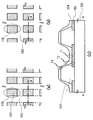
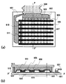
本発明の概念図を図1に示す。図1(a)は基板上にストライプ状(図中縦方向)
の第1電極102aを形成し、画素部110aを形成するために、画素部110aを囲む形で絶縁体隔
壁103aを設け、有機導電体膜104a(図示せず)を形成したものである。
また図1(b)は、基板上にアイランド状の第1電極102bを形成し、画素部110bを形成する
ために、画素部110bを囲む形で絶縁体隔壁103bを設け、有機導電体膜104b(図示せず)を
形成したものである。いずれの場合も、図中A−A'における断面図は図1(c)のようになる
。101は基板、102は第1電極、103は絶縁体隔壁、104は有機導電体膜である。
A conceptual diagram of the present invention is shown in FIG. Fig. 1 (a) shows stripes on the substrate (vertical direction in the figure).
In order to form the first electrode 102a and form the pixel portion 110a, an insulating partition wall 103a is provided so as to surround the pixel portion 110a, and an organic conductor film 104a (not shown) is formed.
In FIG. 1B, an island-shaped first electrode 102b is formed on a substrate, and in order to form the pixel portion 110b, an insulating partition wall 103b is provided so as to surround the pixel portion 110b, and an organic conductor film 104b is formed. (Not shown) is formed. In either case, the cross-sectional view taken along the line AA ′ in the drawing is as shown in FIG. 101 is a substrate, 102 is a first electrode, 103 is an insulator partition, and 104 is an organic conductor film.
この時、有機導電体膜104の厚さ形状は、絶縁体隔壁103の影響により、T2>T1>T3となる
。したがって、T3部分における横方向の抵抗が高くなり、クロストークを防ぐことができ
る。さらに、T2部分が厚くなるため、画素部周辺の電界集中を緩和し、画素部周辺からの
有機発光素子の劣化を防ぐことができる。有機導電体膜104としては、例えばPEDOT/PSSの
ような導電性ポリマーを湿式塗布したものを用いれば良い。
At this time, the thickness shape of the
なお、この形状は、有機導電体膜を湿式塗布する場合に効果的に得られるが、真空蒸着の
ような乾式プロセスによって有機導電体膜を形成する場合も、同様の形状は得られる。し
たがって、有機導電体膜104を形成するプロセスは、乾式プロセス・湿式プロセスいず
れの場合でも有効である。
This shape can be effectively obtained when the organic conductor film is wet-coated, but the same shape can also be obtained when the organic conductor film is formed by a dry process such as vacuum deposition. Therefore, the process for forming the
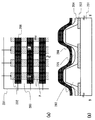
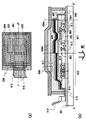
このような概念をパッシブマトリクス型に適用すると、図2のようになる。図2(a)は上
面図、図2(b)は図2(a)中のB−B'の断面図である。すなわち、基板201上にストライプ
状の第1電極202が形成されており、その第1電極202より上方に突き出てなおかつ、画素
部Pを囲む形で絶縁体隔壁203が形成されている。そしてその上に有機導電体膜204(代表
的には導電性ポリマー)が設けられ、さらには電界発光できる有機化合物を含む有機薄膜
205が形成されている。その上に、第1電極と直交する形で、第2電極206が形成されてい
る。
When such a concept is applied to the passive matrix type, it becomes as shown in FIG. 2A is a top view, and FIG. 2B is a cross-sectional view taken along the line BB ′ in FIG. 2A. That is, the stripe-shaped
205 is formed. On top of this, a
なお、ここでは、有機薄膜205はメタルマスクによって画素部ごとに塗り分けられており
、フルカラー表示に適した形態を示している。むろん、単色であれば、塗り分けすること
なくベタ付けしてもよい。
Here, the organic
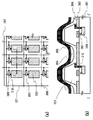
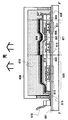
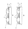
また、このような概念をアクティブマトリクス型に適用すると、図3のようになる。図3
(a)は上面図、図3(b)は図3(a)中のC−C'の断面図である。すなわち、基板301上にアイ
ランド状の第1電極302が形成されており、その第1電極302より上方に突き出てなおかつ
、画素部を囲む形で絶縁体隔壁303が形成されている。そしてその上に有機導電体膜304が
設けられ、さらには電界発光できる有機化合物を含む有機薄膜305が形成されている。そ
の上に、ベタ付けの形で第2電極306が形成されている。
Moreover, when such a concept is applied to the active matrix type, it is as shown in FIG. FIG.
FIG. 3A is a top view, and FIG. 3B is a cross-sectional view taken along the line CC ′ in FIG. That is, an island-shaped
さらに、データ信号ライン307と、走査信号ライン308と、データ信号ライン307および走
査信号ライン308に接続された非線形素子309が設けられており、非線形素子はコンタクト
310により、第1電極302に接続されている。これにより、各画素をそれぞれ単独でスイッ
チすることができる。非線形素子309は代表的には、互いに接続された薄膜トランジスタ
とキャパシタとの組み合わせ、または、薄膜トランジスタと前記薄膜トランジスタの寄生
のキャパシタとの組み合わせ、からなる。
Further, a
The
なお、図2および図3において、有機薄膜の構成としては、公知の有機発光素子の構造を
用いればよい。また、第1電極および第2電極のいずれか一方が可視光透過性を有してい
れば良く、第1電極が陽極の場合は第2電極を陰極に、第1電極が陰極の場合は第2電極
を陽極とすればよい。
2 and 3, the structure of the organic thin film may be a known organic light emitting element structure. In addition, it is sufficient that either one of the first electrode and the second electrode has visible light transmittance. When the first electrode is an anode, the second electrode is a cathode, and when the first electrode is a cathode, the first electrode is a cathode. Two electrodes may be used as anodes.
有機導電体膜としては、有機半導体にアクセプタやドナーをドープして暗導電性を持たせ
る手法が好適である。成膜方法としては、真空蒸着法のような乾式プロセスにて成膜でき
るものと、スピンコートのような湿式プロセスにて成膜できるものがある。
As the organic conductor film, a method of imparting dark conductivity by doping an organic semiconductor with an acceptor or a donor is suitable. As a film forming method, there are a film forming method that can be formed by a dry process such as a vacuum evaporation method and a film forming method that can be formed by a wet process such as spin coating.
乾式プロセスで成膜できる有機導電体膜の一例としては、低分子系の有機半導体と、アク
セプタまたはドナーとを共蒸着する手法が一般的である。p型の有機半導体とアクセプタ
とを共蒸着した場合の有機導電体膜はホール注入層として好ましく、n型の有機半導体と
ドナーとを共蒸着した場合の有機導電体膜は電子注入層として好ましい。
As an example of an organic conductor film that can be formed by a dry process, a technique of co-evaporating a low molecular weight organic semiconductor and an acceptor or a donor is common. An organic conductor film when a p-type organic semiconductor and an acceptor are co-evaporated is preferable as a hole injection layer, and an organic conductor film when an n-type organic semiconductor and a donor are co-evaporated is preferable as an electron injection layer.
低分子系のp型有機半導体としては、4,4'−ビス[N−(1−ナフチル)−N−フェ
ニル−アミノ]−ビフェニル(略称;α−NPD)や、4,4',4''−トリス(N,N−ジ
フェニル−アミノ)−トリフェニルアミン(略称;TDATA)、4,4',4''−トリス[N
−(3−メチルフェニル)−N−フェニル−アミノ]−トリフェニルアミン(略称;MTDA
TA)などの芳香族アミン化合物が挙げられる。また、低分子系のn型有機半導体としては
、トリス(8−キノリノラト)アルミニウム(略称;Alq3)、ビス[2−(2−ヒドロキ
シフェニル)−ベンゾオキサゾラト]亜鉛(略称;Zn(BOX)2)などの金属錯体や、2−(
4−ビフェニリル)−5−(4−tert−ブチルフェニル)−1,3,4−オキサジアゾー
ル(略称;PBD)、1,3−ビス[5−(p−tert−ブチルフェニル)−1,3,4−オキ
サジアゾール−2−イル]ベンゼン(略称;OXD−7)などのオキサジアゾール誘導体、5
−(4−ビフェニリル)−3−(4−tert−ブチルフェニル)−4−フェニル−1,2,
4−トリアゾール(略称;TAZ)、5−(4−ビフェニリル)−3−(4−tert−ブチル
フェニル)−4−(4−エチルフェニル)−1,2,4−トリアゾール(略称;p-EtTAZ
)などのトリアゾール誘導体、バソフェナントロリン(略称;BPhen)・バソキュプロイ
ン(略称;BCP)と記す)などのフェナントロリン誘導体などが挙げられる。
As a low molecular weight p-type organic semiconductor, 4,4′-bis [N- (1-naphthyl) -N-phenyl-amino] -biphenyl (abbreviation: α-NPD), 4,4 ′, 4 ′ '-Tris (N, N-diphenyl-amino) -triphenylamine (abbreviation; TDATA), 4,4', 4 "-Tris [N
-(3-Methylphenyl) -N-phenyl-amino] -triphenylamine (abbreviation; MTDA
And aromatic amine compounds such as TA). As low-molecular n-type organic semiconductors, tris (8-quinolinolato) aluminum (abbreviation: Alq 3 ), bis [2- (2-hydroxyphenyl) -benzoxazolate] zinc (abbreviation: Zn (BOX ) 2 ) and other metal complexes, and 2- (
4-biphenylyl) -5- (4-tert-butylphenyl) -1,3,4-oxadiazole (abbreviation: PBD), 1,3-bis [5- (p-tert-butylphenyl) -1, Oxadiazole derivatives such as 3,4-oxadiazol-2-yl] benzene (abbreviation: OXD-7), 5
-(4-biphenylyl) -3- (4-tert-butylphenyl) -4-phenyl-1,2,
4-triazole (abbreviation; TAZ), 5- (4-biphenylyl) -3- (4-tert-butylphenyl) -4- (4-ethylphenyl) -1,2,4-triazole (abbreviation; p-EtTAZ)
) And the like, and phenanthroline derivatives such as bathophenanthroline (abbreviation: BPhen) and bathocuproin (abbreviation: BCP)).
アクセプタとして有効に機能し、なおかつ蒸着が可能な例としては、TCNQ、TCE、DDQ、ベ
ンゾキノン、2,6−ナフトキノン、p−フルオラニル、テトラクロロジフェノキノン、
ニッケルビスジフェニルグルオキシムなど、ルイス酸として作用するものが代表的である
。ドナーとして有効に機能し、なおかつ蒸着が可能な例としては、TTF、TTT、メチルフェ
ノチアジン、N−イソプロピルカルバゾールなどの有機化合物の他、アルカリ金属、アル
カリ土類金属のようなドナー性の強い金属類など、ルイス塩基として作用するものが代表
的である。
Examples that function effectively as acceptors and that can be deposited include TCNQ, TCE, DDQ, benzoquinone, 2,6-naphthoquinone, p-fluoranil, tetrachlorodiphenoquinone,
A typical example is nickel bisdiphenylglyoxime which acts as a Lewis acid. Examples that can function effectively as a donor and can be deposited include organic compounds such as TTF, TTT, methylphenothiazine, N-isopropylcarbazole, and other metals having strong donor properties such as alkali metals and alkaline earth metals. A typical example is one that acts as a Lewis base.
湿式プロセスで成膜できる有機導電体膜の一例としては、導電性高分子化合物に代表され
るπ共役系を有する高分子化合物と、アクセプタまたはドナーとを混合した溶液を湿式塗
布する手法が一般的である。成膜性が良ければ、高分子化合物ではなく、低分子系の有機
化合物を用いてもよい。この場合も、アクセプタを混合した場合の有機導電体膜はホール
注入層として好ましく、ドナーを混合した場合の有機導電体膜は電子注入層として好まし
い。
As an example of an organic conductor film that can be formed by a wet process, a method of wet coating a solution in which a polymer compound having a π-conjugated system typified by a conductive polymer compound and an acceptor or a donor is mixed is generally used. It is. If the film-forming property is good, a low molecular organic compound may be used instead of the high molecular compound. Also in this case, the organic conductor film when the acceptor is mixed is preferable as the hole injection layer, and the organic conductor film when the donor is mixed is preferable as the electron injection layer.
π共役系を有する高分子化合物の例としては、ポリ(エチレンジオキシチオフェン)(略
称:PEDOT)、ポリアニリン(略称;PAni)、ポリピロールのように実用化されている材
料の他、ポリフェニレン誘導体、ポリチオフェン誘導体、ポリ(パラフェニレンビニレン
)誘導体などがある。
Examples of polymer compounds having a π-conjugated system include poly (ethylenedioxythiophene) (abbreviation: PEDOT), polyaniline (abbreviation: PAni), polypyrrole derivatives, polythiophenes, as well as materials that are put into practical use such as polypyrrole. Derivatives, poly (paraphenylene vinylene) derivatives, and the like.
アクセプタやドナーとしては、上記で挙げたものを用いることもできるが、ポリスチレン
スルホン酸(PSS)のような水溶性ポリマーのアクセプタを用いることで、水溶媒系で湿
式塗布することもできる。PEDOT/PSSやPAni/PSSなどが知られており、特にホール注入層
として有効である。
As the acceptor and donor, those mentioned above can be used, but by using an acceptor of a water-soluble polymer such as polystyrene sulfonic acid (PSS), wet coating can also be performed in an aqueous solvent system. PEDOT / PSS and PAni / PSS are known, and are particularly effective as a hole injection layer.
ところで、図1〜図3の図面上ではテーパー形状の絶縁体隔壁を例に説明しているが、絶
縁体隔壁が他の形状の場合でも、同様の効果、あるいはより大きな効果を得ることができ
る。図1(c)におけるテーパー形状の絶縁体隔壁を、他の形状とした場合の模式図を図
14に示す。
By the way, in the drawings of FIGS. 1 to 3, a taper-shaped insulator partition is described as an example, but the same effect or a larger effect can be obtained even when the insulator partition has another shape. . FIG. 14 shows a schematic diagram in the case where the tapered insulating partition wall in FIG. 1C has another shape.
図14(a)は、絶縁体隔壁103の端部が、絶縁体隔壁103の内側に曲率半径R1を一
つ有する曲面形状となる場合である。つまり、絶縁体隔壁は、絶縁体隔壁の稜線に対して
基板側に曲率半径の中心を少なくとも1つ有する場合であり、前記絶縁体隔壁の稜線は、
変曲点を有さない曲面形状である場合の一例である。
このような場合、図14(a)に示したとおり、絶縁体隔壁の端部は弧を描く形となるた
め、T2>T1>T3の状態を容易に形成することができる。特にT3は、絶縁体隔壁の上端に近
づくにつれ薄くなっていくため、クロストーク防止に大きな効果をもたらす。
FIG. 14A shows a case where the end portion of the
It is an example in the case of a curved surface shape having no inflection points.
In such a case, as shown in FIG. 14A, the end portion of the insulating partition wall has an arcuate shape, so that the state of T2>T1> T3 can be easily formed. In particular, since T3 becomes thinner as it approaches the upper end of the insulator partition wall, it has a great effect on preventing crosstalk.
図14(b)は、絶縁体隔壁103の端部が、絶縁体隔壁103の内側に曲率半径R1を一
つ有すると同時に絶縁体隔壁103の外側にも曲率半径R2を一つ有する曲面形状となる場
合である。つまり、絶縁体隔壁は、絶縁体隔壁の稜線に対して基板側に曲率半径の中心を
少なくとも1つ有し、かつ前記絶縁体隔壁の稜線に対して基板側と反対側に曲率半径の中
心を少なくとも1つ有する場合であり、前記絶縁体隔壁の稜線は、少なくとも1つの変曲
点を有する曲面形状である場合の一例である。このような場合、図14(b)に示したと
おり、絶縁体隔壁の端部はS字型を描く形となるため、同様にT2>T1>T3の状態を容易に
形成することができる。この場合も、T3は絶縁体隔壁の上端に近づくにつれ薄くなってい
くため、クロストーク防止に大きな効果をもたらす。
FIG. 14B shows a curved shape in which the end portion of the
図14に示したような絶縁体隔壁の形状は、スピンコート法により湿式塗布する場合に、
特に効果的である。絶縁体隔壁の端部がなだらかになっているため、スピンコートする際
、液が全面に均一に広がりやすいためである。
The shape of the insulator partition walls as shown in FIG. 14 is obtained when wet coating is applied by a spin coating method.
It is particularly effective. This is because the end of the insulating partition wall is gentle, so that the liquid tends to spread uniformly over the entire surface during spin coating.
なお、有機導電体膜104や204や304に、あらかじめ水素プラズマあるいは水素イオンドー
プなどにより水素原子あるいは水素分子を存在させておき、有機薄膜205や305の成膜後、
加熱等により拡散させておくと、駆動中に有機薄膜205や305において不対結合手(あるい
はラジカル)が生じてしまった場合、それを補修して劣化を防止させるようなことも可能
である。
In addition, hydrogen atoms or hydrogen molecules were previously present in the
If it is diffused by heating or the like, if an unpaired bond (or radical) is generated in the organic
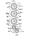
次に、図2や図3の表示装置を形成する装置の概念図を図4に示す。この装置は、有機薄
膜を真空蒸着にて形成する例である。主に基板を搬送する搬送室、受渡を行う受渡室、各
種薄膜を作成する成膜室、封止を行う封止室から構成されている。各室には必要な真空度
を達成するための排気装置、あるいはN2等のガス雰囲気を生成するための装置が装備さ
れており、また各室間はゲートバルブ等で接続されている。基板搬送は搬送ロボットによ
って行われる。
Next, FIG. 4 shows a conceptual diagram of a device for forming the display device of FIG. 2 or FIG. This apparatus is an example of forming an organic thin film by vacuum deposition. It is mainly composed of a transfer chamber for transferring a substrate, a transfer chamber for transferring, a film forming chamber for forming various thin films, and a sealing chamber for sealing. Each chamber is equipped with an exhaust device for achieving a necessary degree of vacuum or a device for generating a gas atmosphere such as N 2 , and the chambers are connected by a gate valve or the like. Substrate transfer is performed by a transfer robot.
最初に、仕込室400に、基板401c(画素部、駆動回路部、配線、電極、保護膜等が
あらかじめ作り込まれているものとするが、ここでは単に「基板」と称す)を外部から導
入する。典型的には、画素部・駆動回路部にはTFTが用いられる。
First, a substrate 401c (a pixel portion, a drive circuit portion, wiring, an electrode, a protective film, etc. are preliminarily formed in the preparation chamber 400, but is simply referred to as “substrate” here) is introduced from the outside. To do. Typically, TFTs are used for the pixel portion and the drive circuit portion.
仕込室400に導入された基板401cは、搬送ロボット401bによって搬送室401
a内に運ばれ、更に前処理室402に搬送される。典型的には、前処理室402で基板4
01cに対して加熱、あるいはO2プラズマ処理などの前処理が行われる。この前処理は
OLEDの諸特性向上を目的としている。また、水溶性の導電性ポリマーなどを有機導電
体膜として塗布する場合は、基板の塗布表面を親水性にし、濡れ性を向上させる役割も果
たす。
The substrate 401c introduced into the preparation chamber 400 is transferred by the transfer robot 401b.
It is carried into a and further conveyed to the
The 01c is heated or pretreated such as O 2 plasma treatment. This pretreatment aims to improve various characteristics of the OLED. In the case where a water-soluble conductive polymer or the like is applied as an organic conductor film, it also serves to improve the wettability by making the coated surface of the substrate hydrophilic.
前処理が終了した基板は、再び仕込み室に戻され、窒素パージを行う。そして、常圧下(
窒素雰囲気)にある搬送室420に運ばれ、反転室422にて基板を表向きに反転させる
。そして、塗布室421にて有機導電体膜(具体的には、PEDOT/PSSのような導電性ポリ
マー)を塗布する。塗布方法は、スピンコートやディップコートなどがあるが、ここでは
スプレー法によって成膜する。塗布後、搬送室420を経由して、反転および真空ベーク
室423へ搬入される。ここでは、反転および真空ベークが行われる。
The substrate for which the pretreatment has been completed is returned to the preparation chamber again, and nitrogen purge is performed. And under normal pressure (
The substrate is transferred to the transfer chamber 420 in a nitrogen atmosphere, and the substrate is inverted in the reverse chamber 422. Then, an organic conductor film (specifically, a conductive polymer such as PEDOT / PSS) is applied in the application chamber 421. Examples of the coating method include spin coating and dip coating. Here, the film is formed by a spray method. After the application, the reversal and vacuum bake chamber 423 is carried through the transfer chamber 420. Here, inversion and vacuum baking are performed.
このように、ここでは真空ベークを反転状態(すなわち、基板表面が下向きとなるフェイ
スダウンの状態)にて行うが、図1や図14で述べたようなT2>T1>T3の関係は、フェイ
スダウンの状態でベークする場合でも問題なく保持されることがわかっている(実施例8
にて後述)。
As described above, the vacuum baking is performed in an inverted state (that is, a face-down state in which the substrate surface faces downward). The relationship of T2>T1> T3 as described in FIG. 1 and FIG. It has been found that even when baking in a down state, it is maintained without any problem (Example 8).
Later).
真空ベーク後、搬送室401aおよび受渡室403を経由して、搬送室404へ運ばれる
。搬送室404にも搬送ロボットが搭載されており、搬送室404に接続されている各部
屋へ基板を搬送する役割を果たす。搬送室404には有機層形成を目的とした成膜室が接
続されている。フルカラー表示のOLED表示装置を作ることを念頭に置いて、R・G・
B各色の発光層を形成するための成膜室406R、406G、406Bが、さらに各色に
共通な層、即ちキャリア輸送層やキャリア注入層等を作成するための成膜室405が設置
されている。これらの成膜室では一般に真空蒸着法が用いられる。フルカラー発光を得る
ためには、R・G・B各色の発光を示す発光層がストライプ状、モザイク状、あるいはデ
ルタ状に配列するように、塗り分け用のシャドウマスクを使用して蒸着を行えばよい。な
お、有機導電体膜をスピンコート法やディップコート法により全面に塗布した場合、各有
機層の成膜を行う前に、前処理室402においてO2プラズマ処理とマスクを組み合わせ
ることにより、有機導電体膜の不必要な部分(封止剤を塗布する部分や配線の上など)を
除去することもできる。
After the vacuum baking, it is carried to the transfer chamber 404 via the transfer chamber 401a and the delivery chamber 403. A transfer robot is also mounted in the transfer chamber 404 and plays a role of transferring a substrate to each room connected to the transfer chamber 404. A film forming chamber for forming an organic layer is connected to the transfer chamber 404. With the goal of creating a full-color OLED display, R, G,
Film formation chambers 406R, 406G, and 406B for forming the light emitting layers of each color B are further provided, and a film formation chamber 405 for forming layers common to the respective colors, that is, a carrier transport layer, a carrier injection layer, and the like. . In these film forming chambers, a vacuum deposition method is generally used. In order to obtain full-color light emission, vapor deposition is performed using a shadow mask for separate coating so that the light-emitting layers that emit light of R, G, and B colors are arranged in stripes, mosaics, or deltas. Good. In the case where the organic conductor film is applied to the entire surface by spin coating or dip coating, the organic conductive film is combined by combining an O 2 plasma treatment and a mask in the
有機層の成膜が終了した基板は、受渡室407を経由して、搬送室408へ運ばれる。搬
送室408にも搬送ロボットが搭載されており、搬送室408に接続されている各部屋へ
基板を搬送する役割を果たす。搬送室408には裏面電極形成や保護膜等形成を目的とし
た成膜室が接続されている。成膜室409や410では、真空蒸着法やEB法で電極とな
る金属(例としてAlLi合金やMgAg合金等)が成膜される。成膜室411では、基
板上面から発光を得る場合に必要な透明導電膜(例としてITOやIZO等)が、一般に
スパッタ法あるいは化学気相成長(CVD:Chemical Vapor Deposition)法で成膜され
る。成膜室412では、表面を保護するためのパッシベーション膜(例としてSiN、S
iOx膜等)が、一般にスパッタ法あるいはCVD法で成膜される。
The substrate on which the organic layer has been formed is transferred to the transfer chamber 408 via the delivery chamber 407. A transfer robot is also mounted in the transfer chamber 408 and plays a role of transferring a substrate to each room connected to the transfer chamber 408. A film forming chamber for the purpose of forming a back electrode or a protective film is connected to the transfer chamber 408. In the film formation chambers 409 and 410, a metal (for example, an AlLi alloy or an MgAg alloy) that serves as an electrode is formed by a vacuum vapor deposition method or an EB method. In the film formation chamber 411, a transparent conductive film (for example, ITO, IZO, etc.) necessary for obtaining light emission from the upper surface of the substrate is generally formed by a sputtering method or a chemical vapor deposition (CVD) method. . In the film formation chamber 412, a passivation film for protecting the surface (for example, SiN, S
In general, an iOx film or the like is formed by sputtering or CVD.
成膜が終了した基板は、受渡室413を経由して、搬送室414へ運ばれる。搬送室41
4には封止を行うために必要な部屋が複数接続されている。搬送室414にも搬送ロボッ
トが搭載されており、搬送室414に接続されている各部屋へ基板あるいは封止基板を搬
送する役割を果たす。
The substrate on which film formation has been completed is carried to the transfer chamber 414 via the delivery chamber 413. Transfer chamber 41
A plurality of rooms necessary for sealing are connected to 4. A transfer robot is also mounted in the transfer chamber 414 and plays a role of transferring a substrate or a sealing substrate to each room connected to the transfer chamber 414.
まず、封止を行うための基板を準備する必要がある。そのための部屋が封止ガラス基板準
備室415a、及び封止プラスチック基板準備室418である。
First, it is necessary to prepare a substrate for sealing. The rooms for that purpose are a sealing glass substrate preparation chamber 415a and a sealing plastic substrate preparation chamber 418.
封止ガラス基板準備室415aには、作成したOLEDをガラス封止するための対向ガラ
スを外部から導入する。必要ならば、OLEDを水から防ぐ乾燥剤を対向ガラスに導入す
ることができる。例えば、シート状の乾燥剤を、あらかじめザグリ加工が施してある対向
ガラスのザグリ部分に両面テープ等で貼りつけておけばよい。
Into the sealing glass substrate preparation chamber 415a, a counter glass for glass sealing the created OLED is introduced from the outside. If necessary, a desiccant that prevents the OLED from water can be introduced into the facing glass. For example, a sheet-like desiccant may be attached to the counterbore portion of the counter glass that has been subjected to counterbore processing in advance with a double-sided tape or the like.
一方、封止プラスチック基板準備室418では、作成したOLEDをプラスチック封止す
るための準備を行う。これらの作業に関しては完全に自動化してもよいし、グローブを設
置して一部手動で行ってもよい。
On the other hand, in the sealing plastic substrate preparation chamber 418, preparation for sealing the produced OLED with plastic is performed. These operations may be completely automated, or may be partially performed manually by installing gloves.
準備された封止ガラス基板あるいは封止プラスチック基板はディスペンサ室416運ばれ
、後に基板と貼り合わせるための接着剤(図示しない)が塗布される。
本実施例では、接着剤として紫外線硬化型のものを用いる。また、必要ならば、OLED
を水から防ぐ乾燥剤(図示しない)を、封止ガラス基板準備室415aにおけるガラス導
入時ではなく、ディスペンサ室416内で仕込んでもよい。例えば、シート状の乾燥剤を
、あらかじめザグリ加工が施してある対向ガラスのザグリ部分に両面テープ等で貼りつけ
ることができる。こうすれば、乾燥剤を大気中で取り扱う必要がなくなる。これらの作業
に関しては、完全に自動化してもよいし、グローブを設置して一部手動で行ってもよい。
特に封止プラスチック基板が曲率及び弾性を有する場合は、曲がった状態で接着剤を塗布
してもよいし、真っ直ぐ伸ばした状態で塗布してもよい。
The prepared sealing glass substrate or sealing plastic substrate is transported to the dispenser chamber 416, and an adhesive (not shown) for later bonding to the substrate is applied.
In this embodiment, an ultraviolet curing type adhesive is used. If necessary, OLED
A desiccant (not shown) for preventing water from being charged may be charged in the dispenser chamber 416 instead of when the glass is introduced into the sealing glass substrate preparation chamber 415a. For example, a sheet-like desiccant can be attached to the counterbore portion of the counter glass that has been subjected to counterbore processing in advance with a double-sided tape or the like. This eliminates the need to handle the desiccant in the atmosphere. These operations may be completely automated, or may be partially manually performed with a glove installed.
In particular, when the sealing plastic substrate has curvature and elasticity, the adhesive may be applied in a bent state, or may be applied in a straightened state.
成膜を終えた基板、及び接着剤が塗布された封止ガラス基板あるいは封止プラスチック基
板は封止室417へ運ばれ、互いに貼り合わせられる。接着時は適当な治具(図示しない
)を用いて加圧する必要がある。曲率及び弾性を有する封止プラスチック基板の場合は真
っ直ぐ伸ばした状態で貼りつければよい。これらの作業に関しては、完全に自動化しても
よいし、グローブを設置して一部手動で行ってもよい。
The substrate after the film formation and the sealing glass substrate or the sealing plastic substrate to which the adhesive is applied are conveyed to the sealing chamber 417 and bonded to each other. At the time of bonding, it is necessary to apply pressure using an appropriate jig (not shown). In the case of a sealed plastic substrate having a curvature and elasticity, it may be attached in a state of being straightened. These operations may be completely automated, or may be partially manually performed with a glove installed.
次いで、封止室417で貼り合わせられた基板および封止基板は紫外光照射室419へ運
ばれ、接着剤硬化のための紫外線が照射させられる。
Next, the substrate and the sealing substrate bonded together in the sealing chamber 417 are conveyed to the ultraviolet light irradiation chamber 419 and irradiated with ultraviolet rays for curing the adhesive.
紫外光照射室419で接着された基板および封止基板は受渡室(図示しない)から外部に
取り出せばよい。
The substrate and the sealing substrate bonded in the ultraviolet light irradiation chamber 419 may be taken out from a delivery chamber (not shown).
本実施例では、本発明で開示した表示装置の例として、パッシブマトリクス型表示装置を
例示する。図5(a)にはその上面図を示し、図5(b)には図5(a)をP−P'で切断した時の断
面図を示す。
In this embodiment, a passive matrix display device is illustrated as an example of the display device disclosed in the present invention. FIG. 5A shows a top view thereof, and FIG. 5B shows a cross-sectional view of FIG. 5A taken along PP ′.
図5(a)において、501は基板であり、ガラスやプラスチック材が用いられる。プラスチッ
ク材としては、ポリイミド、ポリアミド、アクリル樹脂、エポキシ樹脂、PES(ポリエー
テルスルホン)、PC(ポリカーボネート)、PET(ポリエチレンテレフタレート)もしく
はPEN(ポリエーテルニトリル)を板状、もしくはフィルム上にしたものが使用できる。
In FIG. 5A,
502は酸化導電膜からなる走査線(陽極)であり、本実施例では可視光透過性を有するイ
ンジウム錫酸化物(ITO)を用いる。また、506は金属膜を含むデータ線(陰極)であり、
本実施例ではCaF2\Al電極を用い、ストライプ状にパターニングしてある。また、503は
アクリル樹脂からなる絶縁体隔壁である。走査線502とデータ線506は両方とも、ストライ
プ状に複数形成されており、互いに直交するように設けられている。なお、図5(a)では
図示していないが、走査線502とデータ線506の間には導電性ポリマーPEDOT/PSS504および
有機薄膜505が挟まれており、交差部507が画素となる。
In this embodiment, a CaF 2 \ Al electrode is used and patterned in a stripe shape.
そして、走査線502およびデータ線506はTABテープ508を介して外部の駆動回路に接続され
る。なお、509は走査線502が集合してなる配線群を表しており、510はデータ線506に接続
された接続配線511の集合からなる配線群を表す。また、図示していないが、TABテープ50
8の代わりに、TABテープにICを設けたTCPを接続してもよい。
The
Instead of 8, TCP with IC provided on TAB tape may be connected.
また、図5(b)において、512はシール材、513はシール材512により基板501に貼り合わさ
れたカバー材である。シール材512としては例えば光硬化樹脂を用いていればよく、脱ガ
スが少なく、吸湿性の低い材料が望ましい。カバー材としては基板501と同一の材料が好
ましく、ガラス(石英ガラスを含む)もしくはプラスチックを用いることができる。ここ
ではガラスを用いる。
In FIG. 5B, 512 is a sealing material, and 513 is a cover material bonded to the
以上のような構成からなる本発明の表示装置は、画素部514が走査線502、データ線506、
絶縁体隔壁503、導電性ポリマー504、および有機薄膜505で形成されるため、非常に簡単
なプロセスで作製することができる。
In the display device of the present invention having the above structure, the
Since the insulating
また、本実施例に示した表示装置の表示面(画像を観測する面)に偏光板をもうけてもよ
い。この偏光板は、外部から入射した光の反射を押さえ、観測者が表示面に映り込むこと
を防ぐ効果がある。一般的には、円偏光板が用いられている。
ただし、有機化合物膜から発した光が偏光板により反射されて内部に戻ることを防ぐため
、屈折率を調節して内部反射の少ない構造とすることが好ましい。
Further, a polarizing plate may be provided on the display surface (the surface on which an image is observed) of the display device shown in this embodiment. This polarizing plate has an effect of suppressing reflection of light incident from the outside and preventing an observer from being reflected on the display surface. Generally, a circularly polarizing plate is used.
However, in order to prevent light emitted from the organic compound film from being reflected by the polarizing plate and returning to the inside, it is preferable to adjust the refractive index so that the structure has less internal reflection.
本実施例では、本発明で開示した有機発光素子を含む表示装置について説明する。図6で
は、本発明のアクティブマトリクス型表示装置を示す。なお、図6(a)には上面図を示し
、図6(b)には図6(a)をP−P'で切断した時の断面図を示す。
In this example, a display device including the organic light-emitting element disclosed in the present invention will be described. FIG. 6 shows an active matrix display device of the present invention. 6A shows a top view, and FIG. 6B shows a cross-sectional view when FIG. 6A is cut along PP ′.
なお、能動素子としてここでは薄膜トランジスタ(以下、「TFT」と記す)を用いている
が、MOSトランジスタを用いてもよい。また、TFTとしてトップゲート型TFT(具体的には
プレーナ型TFT)を例示するが、ボトムゲート型TFT(典型的には逆スタガ型TFT)を用い
ることもできる。
Note that although a thin film transistor (hereinafter referred to as “TFT”) is used here as an active element, a MOS transistor may be used. Further, although a top gate TFT (specifically, a planar TFT) is exemplified as the TFT, a bottom gate TFT (typically an inverted staggered TFT) can also be used.
図6において、601は基板であり、ここでは基板側から光を取り出すため、可視光を透過
する基板を用いる。具体的には、ガラス基板、石英基板、結晶化ガラス基板もしくはプラ
スチック基板(プラスチックフィルムを含む)を用いればよい。なお、基板601とは、表
面に設けた絶縁膜も含めるものとする。
In FIG. 6,
基板601の上には画素部621および駆動回路622が設けられている。まず、画素部621につい
て説明する。
A
画素部621は画像表示を行う領域である。基板上には複数の画素が存在し、各画素には有
機発光素子に流れる電流を制御するためのTFT(以下、「電流制御TFT」と記す)611、画
素電極(陽極)602、導電性ポリマー膜604、有機薄膜605および陰極606が設けられている
。各画素は、絶縁体隔壁603により囲まれている。なお、612は、電流制御TFTのゲートに
加わる電圧を制御するためのTFT(以下、「スイッチングTFT」と記す)である。
The
電流制御TFT611は、ここではpチャネル型TFTを用いることが好ましい。nチャネル型TFTと
することも可能であるが、図6のように有機発光素子の陽極に電流制御TFTを接続する場
合は、pチャネル型TFTの方が消費電力を押さえることができる。ただし、スイッチングTF
Tはnチャネル型TFTでもpチャネル型TFTでもよい。
Here, the
T may be an n-channel TFT or a p-channel TFT.
また、電流制御TFT611のドレインには画素電極602が電気的に接続されている。
本実施例では、画素電極602の材料として仕事関数が4.5〜5.5eVの導電性材料を用いるた
め、画素電極602は有機発光素子の陽極として機能する。画素電極602として代表的には、
酸化インジウム、酸化錫、酸化亜鉛もしくはこれらの化合物(ITOなど)のような、光透
過性の材料を用いればよい。画素電極602の上には導電性ポリマー膜604、有機薄膜605が
設けられている。
A
In this embodiment, since a conductive material having a work function of 4.5 to 5.5 eV is used as the material of the
A light-transmitting material such as indium oxide, tin oxide, zinc oxide, or a compound thereof (ITO or the like) may be used. A
さらに、有機薄膜605の上には陰極606が設けられている。陰極606の材料としては、仕事
関数が2.5〜3.5eVの導電性材料を用いることが望ましい。陰極606として代表的には、ア
ルカリ金属元素もしくはアルカリ度類金属元素を含む導電膜、アルミニウムを含む導電膜
、あるいはその導電膜にアルミニウムや銀などを積層したもの、を用いればよい。
Further, a
また、陰極606からなる層は、保護膜607で覆われている。保護膜607は、有機発光素子を
酸素および水から保護するために設けられている。保護膜607の材料としては、窒化珪素
、窒化酸化珪素、酸化アルミニウム、酸化タンタル、もしくは炭素(具体的にはダイヤモ
ンドライクカーボン)を用いる。特に、ダイヤモンドライクカーボンを用いた場合、保護
膜607中には水素原子が含まれるため、先に述べたように、加熱等により拡散させておく
と、駆動中に有機薄膜605において不対結合手(あるいはラジカル)が生じてしまった場
合、それを補修して劣化を防止させるようなことも可能である。
Further, the layer made of the
次に、駆動回路622について説明する。駆動回路622は画素部621に伝送される信号(ゲー
ト信号およびデータ信号)のタイミングを制御する領域であり、シフトレジスタ、バッフ
ァ、ラッチ、アナログスイッチ(トランスファゲート)もしくはレベルシフタが設けられ
ている。図6では、これらの回路の基本単位としてnチャネル型TFT613およびpチャネル型
TFT614からなるCMOS回路を示している。
Next, the
The CMOS circuit which consists of TFT614 is shown.
なお、シフトレジスタ、バッファ、ラッチ、アナログスイッチ(トランスファゲート)も
しくはレベルシフタの回路構成は、公知のものでよい。また図6では、同一の基板上に画
素部621および駆動回路622を設けているが、駆動回路622を設けずにICやLSIを電気的に接
続することもできる。
The circuit configuration of the shift register, buffer, latch, analog switch (transfer gate) or level shifter may be a known one. In FIG. 6, the
また、623はゲート信号側駆動回路、622はデータ信号側駆動回路である。また、ゲート信
号側駆動回路623およびデータ信号側駆動回路622に伝送される信号は、データ信号および
走査信号は入力配線615を介してTAB(Tape Automated Bonding)テープ616から入力され
る。なお、図示しないが、TABテープ616の代わりに、TABテープにIC(集積回路)を設け
たTCP(Tape Carrier Package)を接続してもよい。
608は表示装置の上方に設けられるカバー材であり、樹脂からなるシール材609により接着
されている。カバー材608は酸素および水を透過しない材質であれば、いかなるものを用
いてもよい。本実施例では、カバー材608は窪みを持つガラス608aおよび乾燥剤608bから
なる。したがって、シール材609により、有機発光素子を完全に密閉空間610に封入するよ
うになっている。密閉空間610は不活性ガス(代表的には窒素ガスや希ガス)、樹脂また
は不活性液体(例えばパーフルオロアルカンに代表される液状のフッ素化炭素)を充填し
ておけばよい。さらに、吸湿剤や脱酸素剤を設けることも有効である。
A
なお、図6では電流制御TFT611に画素電極(陽極)602が電気的に接続されているが、陰
極が電流制御TFTに接続された構造をとることもできる。その場合、画素電極を陰極606と
同様の材料で形成し、陰極を画素電極(陽極)602と同様の材料で形成すればよい。その
場合、電流制御TFTはnチャネル型TFTとすることが好ましい。
In FIG. 6, the pixel electrode (anode) 602 is electrically connected to the
また、本実施例に示した表示装置の表示面(画像を観測する面)に偏光板をもうけてもよ
い。この偏光板は、外部から入射した光の反射を押さえ、観測者が表示面に映り込むこと
を防ぐ効果がある。一般的には、円偏光板が用いられている。
ただし、有機化合物膜から発した光が偏光板により反射されて内部に戻ることを防ぐため
、屈折率を調節して内部反射の少ない構造とすることが好ましい。
Further, a polarizing plate may be provided on the display surface (the surface on which an image is observed) of the display device shown in this embodiment. This polarizing plate has an effect of suppressing reflection of light incident from the outside and preventing an observer from being reflected on the display surface. Generally, a circularly polarizing plate is used.
However, in order to prevent light emitted from the organic compound film from being reflected by the polarizing plate and returning to the inside, it is preferable to adjust the refractive index so that the structure has less internal reflection.
本実施例では、本発明の表示装置の例として、アクティブマトリクス型表示装置を例示す
るが、実施例2とは異なり、能動素子が形成されている基板とは反対側から光を取り出す
構造(以下、「上方出射」と記す)の表示装置を示す。図7にその断面図を示す。
In this embodiment, an active matrix display device is illustrated as an example of the display device of the present invention. Unlike
なお、能動素子としてここでは薄膜トランジスタ(以下、「TFT」と記す)を用いている
が、MOSトランジスタを用いてもよい。また、TFTとしてトップゲート型TFT(具体的には
プレーナ型TFT)を例示するが、ボトムゲート型TFT(典型的には逆スタガ型TFT)を用い
ることもできる。
Note that although a thin film transistor (hereinafter referred to as “TFT”) is used here as an active element, a MOS transistor may be used. Further, although a top gate TFT (specifically, a planar TFT) is exemplified as the TFT, a bottom gate TFT (typically an inverted staggered TFT) can also be used.
本実施例において、第1電極、第2電極、保護膜、カバー材以外の構成は、実施例2と同
様でよい。
In the present embodiment, the configuration other than the first electrode, the second electrode, the protective film, and the cover material may be the same as in the second embodiment.
電流制御TFT611のドレインに接続されている第一電極602であるが、本実施例では陽極と
して用いるため、仕事関数がより大きい導電性材料を用いることが好ましい。その代表例
として、ニッケル、パラジウム、タングステン、金、銀などの金属が挙げられる。本実施
例では、第一電極602は光を透過しないことが好ましいが、それに加えて、光の反射性の
高い材料を用いることがさらに好ましい。
The
また、本実施例は上方出射であるため、第二電極606が光透過性であることが大前提であ
る。したがって、これらの金属を用いる場合は、20nm程度の超薄膜であることが好ましい
。
Further, since the present embodiment is upward emission, it is a major premise that the
また、保護膜607は、有機発光素子を酸素および水から保護するために設けられている。
本実施例では、光を透過するものであればいかなるものを用いてもよい。
The protective film 607 is provided to protect the organic light emitting element from oxygen and water.
In this embodiment, any material that transmits light may be used.
さらに、608はカバー材であり、樹脂からなるシール材609により接着されている。カバー
材608は酸素および水を透過しない材質で、かつ、光を透過する材質であればいかなるも
のを用いてもよい。本実施例ではガラスを用いる。密閉空間610は不活性ガス(代表的に
は窒素ガスや希ガス)、樹脂または不活性液体(例えばパーフルオロアルカンに代表され
る液状のフッ素化炭素)を充填しておけばよい。さらに、吸湿剤や脱酸素剤を設けること
も有効である。
Further,
なお、図7では電流制御TFT611に第一電極(陽極)602が電気的に接続されているが、陰
極が電流制御TFTに接続された構造をとることもできる。その場合、第一電極を陰極の材
料で形成し、第二電極を陽極の材料で形成すればよい。このとき、電流制御TFTはnチャネ
ル型TFTとすることが好ましい。
In FIG. 7, the first electrode (anode) 602 is electrically connected to the
本実施例では、実施例2および実施例3で示したような表示装置を、デジタル時間階調表
示により駆動する例を示す。
In this embodiment, an example in which the display device as shown in
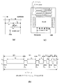
有機発光素子を用いた画素の、回路構成を図8(a)に示す。Trはトランジスタ、Csはスト
レージキャパシタを表す。図8(a)中の回路構成では、ソース線はトランジスタTr1のソー
ス側に、ゲート線はトランジスタTr1のゲートに接続されている。また、電源供給線はス
トレージキャパシタCs、およびトランジスタTr2のソース側に接続されている。トランジ
スタTr2のドレイン側には本発明の有機発光素子の陽極が接続されているため、有機発光
素子を挟んでトランジスタTr2の反対側は、陰極となっている。
FIG. 8A shows a circuit configuration of a pixel using an organic light emitting element. Tr represents a transistor, and Cs represents a storage capacitor. In the circuit configuration in FIG. 8A, the source line is connected to the source side of the transistor Tr1, and the gate line is connected to the gate of the transistor Tr1. The power supply line is connected to the storage capacitor Cs and the source side of the transistor Tr2. Since the anode of the organic light emitting element of the present invention is connected to the drain side of the transistor Tr2, the opposite side of the transistor Tr2 across the organic light emitting element is a cathode.
この回路においては、ゲート線が選択されると、電流がソース線からTr1に流れ、その信
号に対応する電圧がCsに蓄積される。そして、Tr2のゲートおよびソース間の電圧(Vgs)
により制御される電流が、Tr2および有機発光素子に流れることになる。
In this circuit, when a gate line is selected, a current flows from the source line to Tr1, and a voltage corresponding to the signal is accumulated in Cs. And the voltage between the gate and source of Tr2 (V gs )
The current controlled by the current flows through Tr2 and the organic light emitting element.
Tr1が選択されたあとは、Tr1はオフ状態となり、Csの電圧(Vgs)が保持される。したが
って、Vgsに依存するだけの電流を流し続けることができる。
After Tr1 is selected, Tr1 is turned off and the Cs voltage (V gs ) is maintained. Therefore, it is possible to continue flowing a current that depends on V gs .
このような回路を、デジタル時間階調表示により駆動するチャートを図8(b)に示す。す
なわち、1フレームを複数のサブフレームに分割するわけだが、図8(b)では、1フレー
ムを6つのサブフレーム(SF1〜SF6)に分割する6ビット階調とした。TAは書き込み時間
である。この場合、それぞれのサブフレーム発光期間の割合は、図に示したように32:
16:8:4:2:1となる。
FIG. 8B shows a chart for driving such a circuit by digital time gray scale display. That is, one frame is divided into a plurality of subframes. In FIG. 8B, a 6-bit gradation is used to divide one frame into six subframes (SF1 to SF6). TA is the write time. In this case, the ratio of each sub-frame light emission period is 32:
16: 8: 4: 2: 1.
本実施例におけるTFT基板の駆動回路の概要を図8(c)に示す。図8(c)中の基板構成では
、本発明の有機発光素子を各画素とした画素部に対し、図8(a)で示したような電源供給
線および陰極が接続されている。また、シフトレジスタは、シフトレジスタ→ラッチ1→
ラッチ2→画素部の順で、画素部に接続されている。
ラッチ1にはデジタル信号が入力され、ラッチ2に入力されるラッチパルスによって画像
データを画素部に送り込むことができる。
The outline of the TFT substrate drive circuit in this embodiment is shown in FIG. In the substrate configuration in FIG. 8 (c), the power supply line and the cathode as shown in FIG. 8 (a) are connected to the pixel portion having the organic light emitting device of the present invention as each pixel. The shift register is shift register → latch 1 →
They are connected to the pixel portion in the order of
A digital signal is input to the latch 1, and image data can be sent to the pixel portion by a latch pulse input to the
ゲートドライバおよびソースドライバは同じ基板上に設けられている。本実施例では、画
素回路およびドライバは、デジタル駆動するように設計されているため、TFT特性のばら
つきの影響を受けることなく、均一な像を得ることができる。
The gate driver and the source driver are provided on the same substrate. In this embodiment, since the pixel circuit and the driver are designed to be digitally driven, a uniform image can be obtained without being affected by variations in TFT characteristics.
上記実施例で述べた本発明の表示装置は、低消費電力で寿命が長いという利点を有する。
したがって、前記表示装置が表示部等として含まれる電気器具は、従来よりも低い消費電
力で動作可能であり、なおかつ長保ちする電気器具となる。特に電源としてバッテリーを
使用する携帯機器のような電気器具に関しては、低消費電力化が便利さに直結する(電池
切れが起こりにくい)ため、極めて有用である。
The display device of the present invention described in the above embodiment has an advantage of low power consumption and long life.
Therefore, an electric appliance in which the display device is included as a display unit or the like is an electric appliance that can operate with lower power consumption than the conventional one and keep it long. In particular, an electric appliance such as a portable device that uses a battery as a power source is extremely useful because low power consumption is directly linked to convenience (battery is unlikely to run out).
また、前記表示装置は、自発光型であることから液晶表示装置のようなバックライトは必
要なく、有機化合物膜の厚みも1μmに満たないため、薄型軽量化が可能である。したが
って、前記表示装置が表示部等として含まれる電気器具は、従来よりも薄型軽量な電気器
具となる。このことも、特に携帯機器のような電気器具に関して、便利さ(持ち運びの際
の軽さやコンパクトさ)に直結するため、極めて有用である。さらに、電気器具全般にお
いても、薄型である(かさばらない)ことは運送面(大量輸送が可能)、設置面(部屋な
どのスペース確保)からみても有用であることは疑いない。
Further, since the display device is a self-luminous type, a backlight as in a liquid crystal display device is not necessary, and the thickness of the organic compound film is less than 1 μm, so that the thickness and weight can be reduced. Therefore, an electric appliance in which the display device is included as a display unit or the like is an electric appliance that is thinner and lighter than conventional ones. This is also extremely useful because it is directly connected to convenience (lightness and compactness when carrying), especially with respect to electric appliances such as portable devices. Furthermore, there is no doubt that the thinness (not bulky) of electrical appliances in general is also useful from the viewpoint of transportation (capable of mass transportation) and installation (serving space such as rooms).
なお、前記表示装置は自発光型であるために、液晶表示装置に比べて明るい場所での視認
性に優れ、しかも視野角が広いという特徴を持つ。したがって、前記表示装置を表示部と
して有する電気器具は、表示の見やすさの点でも大きなメリットがある。
Since the display device is a self-luminous type, the display device is superior in visibility in a bright place as compared with the liquid crystal display device and has a wide viewing angle. Therefore, an electric appliance having the display device as a display unit has a great merit in viewability of display.
すなわち、本発明の表示装置を用いた電気器具は、薄型軽量・高視認性といった従来の有
機発光素子の長所に加え、低消費電力・長寿命という特長も保有しており、極めて有用で
ある。
That is, the electric appliance using the display device of the present invention is extremely useful because it has the advantages of low power consumption and long life in addition to the advantages of the conventional organic light emitting device such as thin and light weight and high visibility.
本実施例では、本発明の表示装置を表示部として含む電気器具を例示する。その具体例を
図9および図10に示す。なお、本実施例の電気器具に含まれる有機発光素子には、本発
明で開示した素子のいずれを用いてもよい。また、本実施例の電気器具に含まれる表示装
置の形態は、図2、図3、図5〜図8のいずれの形態を用いても良い。
In this example, an electric appliance including the display device of the present invention as a display unit is illustrated. Specific examples thereof are shown in FIGS. In addition, any of the elements disclosed in the present invention may be used as the organic light-emitting element included in the electric appliance of this example. In addition, as the form of the display device included in the electric appliance of the present embodiment, any form of FIGS. 2, 3, and 5 to 8 may be used.
図9(a)は有機発光素子を用いたディスプレイであり、筐体901a、支持台902a、表示部903
aを含む。本発明の表示装置を表示部903aとして用いたディスプレイを作製することによ
り、薄く軽量で、長保ちするディスプレイを実現できる。よって、輸送が簡便になり、設
置の際の省スペースが可能となる上に、寿命も長い。
FIG. 9A illustrates a display using an organic light emitting element, which includes a housing 901a, a
Includes a. By manufacturing a display using the display device of the present invention as the display portion 903a, a thin, light, and long display can be realized. Therefore, transportation becomes simple, space saving during installation is possible, and the service life is also long.
図9(b)はビデオカメラであり、本体901b、表示部902b、音声入力部903b、操作スイッチ9
04b、バッテリー905b、受像部906bを含む。本発明の表示装置を表示部902bとして用いた
ビデオカメラを作製することにより、消費電力が少なく、軽量なビデオカメラを実現でき
る。よって、電池の消費量が少なくなり、持ち運びも簡便になる。
FIG. 9B shows a video camera, which includes a
04b, a
図9(c)はデジタルカメラであり、本体901c、表示部902c、接眼部903c、操作スイッチ904
cを含む。本発明の表示装置を表示部902cとして用いたデジタルカメラを作製することに
より、消費電力が少なく、軽量なデジタルカメラを実現できる。よって、電池の消費量が
少なくなり、持ち運びも簡便になる。
FIG. 9C illustrates a digital camera, which includes a
c included. By manufacturing a digital camera using the display device of the present invention as the
図9(d)は記録媒体を備えた画像再生装置であり、本体901d、記録媒体(CD、LD、またはD
VDなど)902d、操作スイッチ903d、表示部(A)904d、表示部(B)905dを含む。表示部(A)904
dは主として画像情報を表示し、表示部(B)905dは主として文字情報を表示する。本発明の
表示装置をこれら表示部(A)904dや表示部(B)905dとして用いた前記画像再生装置を作製す
ることにより、消費電力が少なく軽量な上に、長保ちする前記画像再生装置を実現できる
。なお、この記録媒体を備えた画像再生装置には、CD再生装置、ゲーム機器なども含む。
FIG. 9 (d) shows an image reproducing apparatus provided with a recording medium. The
VD etc.) 902d,
“d” mainly displays image information, and the display unit (B) 905d mainly displays character information. By producing the image reproduction device using the display device of the present invention as the display unit (A) 904d and the display unit (B) 905d, the image reproduction device that is low in power consumption and is long in length can be obtained. realizable. Note that the image reproducing device provided with the recording medium includes a CD reproducing device, a game machine, and the like.
図9(e)は携帯型(モバイル)コンピュータであり、本体901e、表示部902e、受像部903e
、操作スイッチ904e、メモリスロット905eを含む。本発明の表示装置を表示部902eとして
用いた携帯型コンピュータを作製することにより、消費電力が少なく、薄型軽量な携帯型
コンピュータを実現できる。よって、電池の消費量が少なくなり、持ち運びも簡便になる
。なお、この携帯型コンピュータはフラッシュメモリや不揮発性メモリを集積化した記録
媒体に情報を記録したり、それを再生したりすることができる。
FIG. 9E shows a portable (mobile) computer, which includes a
図9(f)はパーソナルコンピュータであり、本体901f、筐体902f、表示部903f、キーボー
ド904fを含む。本発明の表示装置を表示部903fとして用いたパーソナルコンピュータを作
製することにより、消費電力が少なく、薄型軽量なパーソナルコンピュータを実現できる
。特に、ノートパソコンのように持ち歩く用途が必要な場合、電池の消費量や軽さの点で
大きなメリットとなる。
FIG. 9F shows a personal computer, which includes a
なお、上記電気器具はインターネットなどの電子通信回線や電波などの無線通信を通じて
配信される情報を表示することが多くなってきており、特に動画情報を表示する機会が増
えている。有機発光素子の応答速度は非常に速く、そのような動画表示に好適である。
In addition, the electric appliances often display information distributed through an electronic communication line such as the Internet or wireless communication such as radio waves, and in particular, opportunities for displaying moving image information are increasing. The response speed of the organic light emitting device is very fast, and it is suitable for such moving image display.
次に、図10(a)は携帯電話であり、本体1001a、音声出力部1002a、音声入力部1003a、表
示部1004a、操作スイッチ1005a、アンテナ1006aを含む。本発明の表示装置を表示部1004a
として用いた携帯電話を作製することにより、消費電力が少なく、薄型軽量な携帯電話を
実現できる。よって、電池の消費量が少なくなり、持ち運びも楽になる上にコンパクトな
本体にできる。
Next, FIG. 10A shows a mobile phone, which includes a
By manufacturing the mobile phone used as the mobile phone, a thin and light mobile phone with low power consumption can be realized. Therefore, the battery consumption is reduced, the carrying becomes easier and the body can be made compact.
図10(b)は音響機器(具体的には車載用オーディオ)であり、本体1001b、表示部1002b
、操作スイッチ1003b、1004bを含む。本発明の表示装置を表示部1002bとして用いた音響
機器を作製することにより、消費電力が少なく、軽量な音響機器を実現できる。また、本
実施例では車載用オーディオを例として示すが、家庭用オーディオに用いても良い。
FIG. 10B shows an acoustic device (specifically, an on-vehicle audio), which includes a
, Including operation switches 1003b and 1004b. By manufacturing an acoustic device using the display device of the present invention as the
なお、図9〜図10で示したような電気器具において、さらに光センサを内蔵させ、使用
環境の明るさを検知する手段を設けることで、使用環境の明るさに応じて発光輝度を変調
させるような機能を持たせることは有効である。使用者は、使用環境の明るさに比べてコ
ントラスト比で100〜150の明るさを確保できれば、問題なく画像もしくは文字情報を認識
できる。すなわち、使用環境が明るい場合は画像の輝度を上げて見やすくし、使用環境が
暗い場合は画像の輝度を抑えて消費電力を抑えるといったことが可能となる。
In addition, in the electric appliances as shown in FIGS. 9 to 10, the light emission luminance is modulated according to the brightness of the use environment by further incorporating a light sensor and providing means for detecting the brightness of the use environment. It is effective to have such a function. The user can recognize the image or the character information without any problem if the brightness of 100 to 150 can be secured in the contrast ratio as compared with the brightness of the usage environment. That is, when the usage environment is bright, it is possible to increase the brightness of the image for easy viewing, and when the usage environment is dark, the brightness of the image can be suppressed to reduce power consumption.
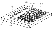
導電性ポリマーはスピン塗布法などで全面に塗布せずとも、ディスペンサーやインクジェ
ット法を用いてストライプ状に形成しても良い。図11は基板1101上にデータ線駆動回路
1104が形成され、画素部1102にインクジェット法で導電性ポリマー1106を形成する様子を
示している。画素部1102にはストライプ状に隔壁1105が設けられ、各隔壁の間に導電性ポ
リマー1106を形成する。隔壁1105はインクジェット法で有機化合物層を形成する際に、隣
接する有機化合層が相互に混ざり合わないようにするために設けている。
The conductive polymer may be formed in a stripe shape using a dispenser or an ink jet method without being applied to the entire surface by a spin coating method or the like. FIG. 11 shows a data line driving circuit on a
1104 is formed and a
導電性ポリマー1106は、インクヘッド1107から導電性ポリマーを含む組成物を吐出して形
成する。この組成物はインクヘッドから連続的に吐出させて、線状のパターンを形成する
。
The
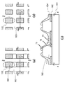
図12(a)は基板上にストライプ状(図中縦方向)の第1電極102aを形成し、画素部110a
を形成するために、画素部110aを囲む形で絶縁体隔壁103aを設けたものである。また図1
2(b)は、基板上にアイランド状の第1電極102bを形成し、画素部110bを形成するために
、画素部110bを囲む形で絶縁体隔壁103bを設けたものである。いずれの場合も、図中A−A
'における断面図は図12(c)のようになる。
即ち、隔壁の間に導電性ポリマー104を形成することができ、隔壁103上には必ずしも形成
されず分離させることができる。この導電性ポリマー層上には低分子有機化合物材料で形
成される発光層、電子注入輸送層などを形成すれば良い。
In FIG. 12A, a first electrode 102a having a stripe shape (vertical direction in the figure) is formed on a substrate, and a pixel portion 110a is formed.
In order to form this, an insulating partition wall 103a is provided so as to surround the pixel portion 110a. Figure 1
In FIG. 2B, an island-shaped first electrode 102b is formed on a substrate, and an insulator partition wall 103b is provided so as to surround the pixel portion 110b in order to form the pixel portion 110b. In either case, A-A in the figure
The cross-sectional view at 'is as shown in FIG.
That is, the
その場合においても、導電性ポリマー104の厚さ形状は、絶縁体隔壁103の影響により、T2
>T1>T3となる。したがって、T3部分における横方向の抵抗が高くなり、クロストークを
防ぐことができる。さらに、T2部分が厚くなるため、画素部周辺の電界集中を緩和し、画
素部周辺からの有機発光素子の劣化を防ぐことができる。
Even in that case, the thickness shape of the
>T1> T3. Therefore, the lateral resistance at the T3 portion is increased, and crosstalk can be prevented. Further, since the T2 portion is thick, the electric field concentration around the pixel portion can be alleviated, and deterioration of the organic light emitting element from around the pixel portion can be prevented.
本実施例ではアクティブマトリクス型表示装置を作製する例を示す。 In this embodiment, an example of manufacturing an active matrix display device is shown.
まず、絶縁表面上に複数のTFT(スイッチング用TFTや電流制御用TFTを含む)
、保持容量、電流制御用TFTに接続する第1の電極(陽極)、該第1の電極の端部を覆
う隔壁を形成する。第1の電極の材料としては、Ti、TiN、TiSiXNY、Ni、W
、WSiX、WNX、WSiXNY、NbN、Mo、Cr、Pt、あるいはTi、Si、Ni
、W、Nb、Cr、Zn、Sn、In、Moから選ばれた元素を主成分とする合金材料も
しくは化合物材料を用いればよい。
また、第1の電極は、これらの材料を用いた膜またはそれらの積層膜を総膜厚100nm
〜800nmの範囲で用いればよい。また、カバレッジを良好なものとするため、隔壁の
上端部または下端部に曲率を有する曲面が形成されるようにする。例えば、隔壁の材料と
してポジ型の感光性アクリルを用いた場合、絶縁物1114の上端部のみに曲率半径(0
.2μm〜3μm)を有する曲面を持たせることが好ましい。また、隔壁として、感光性
の光によってエッチャントに不溶解性となるネガ型、或いは光によってエッチャントに溶
解性となるポジ型のいずれも使用することができる。
First, a plurality of TFTs (including switching TFTs and current control TFTs) on the insulating surface
A first electrode (anode) connected to the storage capacitor and the current control TFT and a partition wall covering the end portion of the first electrode are formed. As the material of the first electrode, Ti, TiN, TiSi x N y , Ni, W
, WSi x , WN x , WSi x N y , NbN, Mo, Cr, Pt, or Ti, Si, Ni
An alloy material or a compound material whose main component is an element selected from W, Nb, Cr, Zn, Sn, In, and Mo may be used.
The first electrode is formed of a film using these materials or a stacked film thereof with a total film thickness of 100 nm.
What is necessary is just to use in the range of -800 nm. In order to improve the coverage, a curved surface having a curvature is formed at the upper end portion or the lower end portion of the partition wall. For example, when positive photosensitive acrylic is used as a material for the partition wall, only the upper end portion of the insulator 1114 has a curvature radius (0
. It is preferable to have a curved surface having 2 μm to 3 μm. As the partition wall, either a negative type that becomes insoluble in an etchant by photosensitive light or a positive type that becomes soluble in an etchant by light can be used.
次いで、隔壁で覆われていない第1の電極の表面に塗布法による正孔注入層を形成する。
例えば、正孔注入層として作用するポリ(エチレンジオキシチオフェン)/ポリ(スチレ
ンスルホン酸)水溶液(PEDOT/PSS)をスピンコート法で全面に塗布、焼成する。正孔注
入層を塗布法で形成した後、蒸着法による成膜直前に真空加熱(100〜200℃)を行
うことが好ましい。なお、例えば、第1の電極(陽極)の表面をスポンジで洗浄した後、
スピンコート法でポリ(エチレンジオキシチオフェン)/ポリ(スチレンスルホン酸)水
溶液(PEDOT/PSS)を全面に設定膜厚60nm、80℃、10分間で仮焼成、200℃、
1時間で本焼成し、さらに蒸着直前に真空加熱(170℃、加熱30分、冷却30分)し
て大気に触れることなく蒸着法で発光層を含む有機薄膜の形成を行う。特に、ITO膜を
第1の電極の材料として用い、表面に凹凸や微小な粒子が存在している場合、PEDOT/PSS
の膜厚を30nm以上の膜厚とすることでこれらの影響を低減することができ、結果的に
点欠陥を減少させる。
Next, a hole injection layer is formed by a coating method on the surface of the first electrode not covered with the partition walls.
For example, a poly (ethylenedioxythiophene) / poly (styrenesulfonic acid) aqueous solution (PEDOT / PSS) that acts as a hole injection layer is applied to the entire surface by a spin coating method and baked. After the hole injection layer is formed by a coating method, it is preferable to perform vacuum heating (100 to 200 ° C.) immediately before film formation by a vapor deposition method. For example, after cleaning the surface of the first electrode (anode) with a sponge,
A poly (ethylenedioxythiophene) / poly (styrenesulfonic acid) aqueous solution (PEDOT / PSS) is set on the entire surface by spin coating. Film thickness 60 nm, pre-baked at 80 ° C. for 10 minutes, 200 ° C.
The main calcination is performed for 1 hour, and vacuum heating (170 ° C., heating for 30 minutes, cooling for 30 minutes) is performed immediately before vapor deposition to form an organic thin film including a light emitting layer by vapor deposition without exposure to the atmosphere. In particular, when ITO film is used as the material for the first electrode and there are irregularities and fine particles on the surface, PEDOT / PSS
These effects can be reduced by setting the film thickness to 30 nm or more, resulting in a decrease in point defects.
また、PEDOT/PSSはITO膜上に塗布すると濡れ性があまりよくないため、PEDOT/PSS
溶液をスピンコート法で1回目の塗布を行った後、一旦純水で洗浄することによって濡れ
性を向上させ、再度、PEDOT/PSS溶液をスピンコート法で2回目の塗布を行い、焼成を行
って均一性良く成膜することが好ましい。なお、1回目の塗布を行った後、一旦純水で洗
浄することによって表面を改質するとともに、微小な粒子なども除去できる効果が得られ
る。
In addition, PEDOT / PSS is not so good when applied on ITO film, so PEDOT / PSS
After the solution is first applied by spin coating, the wettability is improved by washing with pure water once, and the PEDOT / PSS solution is applied again by spin coating for the second time and then baked. It is preferable to form a film with good uniformity. In addition, after performing the 1st application | coating, while washing | cleaning with a pure water once, while modifying the surface, the effect which can remove a micro particle etc. is acquired.
また、スピンコート法によりPEDOT/PSSを成膜した場合、全面に成膜されるため、基板
の端面や周縁部、端子部、陰極と下部配線との接続領域などは選択的に除去することが好
ましく、O2アッシングなどで除去することが好ましい。
In addition, when PEDOT / PSS is formed by spin coating, the film is formed over the entire surface, so that the end face, peripheral edge, terminal part, connection area between the cathode and lower wiring, etc. can be selectively removed. Preferably, it is preferably removed by O 2 ashing or the like.
次いで、有機薄膜上に第2の電極(陰極)を形成する。第2の電極としては、仕事関数の
小さい材料(Al、Ag、Li、Ca、またはこれらの合金MgAg、MgIn、AlL
i、CaF2、またはCaN)を用いればよい。なお、第2の電極は、TFTにダメージ
が少ない抵抗加熱法で蒸着を行うことが好ましい。
Next, a second electrode (cathode) is formed on the organic thin film. As the second electrode, a material having a small work function (Al, Ag, Li, Ca, or an alloy thereof MgAg, MgIn, AlL
i, CaF 2 , or CaN) may be used. Note that the second electrode is preferably deposited by a resistance heating method with little damage to the TFT.
また、図13(A)は、第2の電極形成後の素子を切断して観察したTEM写真である
。なお、図13(B)は図13(A)に対応する模式図である。なお、図13(A)にお
いて、第1の電極上にはPEDOT/PSSが90nm程度形成されている。
FIG. 13A is a TEM photograph obtained by observing the element after forming the second electrode. FIG. 13B is a schematic diagram corresponding to FIG. In FIG. 13A, PEDOT / PSS is formed to approximately 90 nm on the first electrode.
本実施例では、隔壁の上端部または下端部に曲率を有する曲面を形成することで、スピ
ンコート法であっても、隔壁のなだらかな側壁において、第1の電極から離れるに従って
膜厚を薄くし、好ましくは、隔壁上部には正孔注入層である導電性ポリマーがない構造と
することを特徴としている。
In this example, a curved surface having a curvature is formed at the upper end or the lower end of the partition wall, so that the film thickness is reduced as the distance from the first electrode increases on the gentle side wall of the partition wall even in the spin coating method. Preferably, the structure is characterized in that there is no conductive polymer as a hole injection layer above the partition wall.
図13(A)に示すように、隔壁のなだらかな側壁には薄くあるものの隔壁上部には正
孔注入層であるPEDOT/PSSが確認できず、図13(A)に示す構造とすることで効果的に
クロストークの発生を抑えることができる。
As shown in FIG. 13A, although the thin side wall of the partition wall is thin, PEDOT / PSS which is a hole injection layer cannot be confirmed in the upper part of the partition wall, and the structure shown in FIG. The occurrence of crosstalk can be effectively suppressed.
また、本実施例は、実施の形態、実施例1乃至6のいずれか一と自由に組み合わせるこ
とができる。
In addition, this embodiment can be freely combined with any one of the embodiment mode and Embodiments 1 to 6.
図4に示すような装置を用いて本発明の有機発光装置を作製する場合、導電性ポリマーな
どの有機導電体膜を塗布後、ベークする際は、塗布面を下、すなわちフェイスダウンの状
態でベークする状況となる。本実施例では、そのようなベーク法であっても、実施例7の
ような形状が得られることを確認する実験を行った。
When the organic light-emitting device of the present invention is manufactured using an apparatus as shown in FIG. 4, when an organic conductor film such as a conductive polymer is applied and then baked, the application surface is down, that is, face-down state. Bake situation. In this example, an experiment was conducted to confirm that the shape as in Example 7 was obtained even with such a baking method.
まず、図13に示したものと同じ形状の絶縁体隔壁を有する基板に、PEDOT/PSSをスピン
コート法により塗布し、その後塗布面を下向きにして200℃にてベークを行い、断面TE
Mにて形状を観察した。その様子を図15に示す。1501はITO、1502はPEDOT/P
SSの層、その上のやや白みがかった層1503は保護層(カーボン層)である。
First, PEDOT / PSS is applied to a substrate having an insulating partition having the same shape as that shown in FIG. 13 by spin coating, followed by baking at 200.degree.
The shape was observed with M. This is shown in FIG. 1501 is ITO, 1502 is PEDOT / P
The SS layer, and the slightly whitish layer 1503 thereon, is a protective layer (carbon layer).
図15の通り、有機導電体膜を湿式塗布後フェイスダウンにてベークする場合でも、図1
3と全く同様の形状が得られることが確認できた。したがって、本発明の特徴である形状
は、ベーク時の基板の向きによらず形成できる。
As shown in FIG. 15, even when the organic conductor film is baked face-down after wet coating, FIG.
It was confirmed that the same shape as that of No. 3 was obtained. Therefore, the shape that is a feature of the present invention can be formed regardless of the orientation of the substrate during baking.
本実施例では、上面出射構造の発光装置の一例を例示する。その概略図を図16に示す
。
In this embodiment, an example of a light emitting device having a top emission structure is illustrated. A schematic diagram thereof is shown in FIG.
図16(A)は、発光装置を示す上面図、図16(B)は図16(A)をA−A’で切
断した断面図である。点線で示された1601はソース信号線駆動回路、1602は画素
部、1603はゲート信号線駆動回路である。また、1604は透明な封止基板、160
5は第1のシール材であり、第1のシール材1605で囲まれた内側は、透明な第2のシ
ール材1607で充填されている。なお、第1のシール材1605には基板間隔を保持す
るためのギャップ材が含有されている。
16A is a top view illustrating the light-emitting device, and FIG. 16B is a cross-sectional view taken along line AA ′ in FIG. 16A. Reference numeral 1601 indicated by a dotted line denotes a source signal line driver circuit, 1602 denotes a pixel portion, and 1603 denotes a gate signal line driver circuit. 1604 is a transparent sealing substrate, 160
Reference numeral 5 denotes a first sealing material, and the inside surrounded by the first sealing material 1605 is filled with a transparent second sealing material 1607. Note that the first sealing material 1605 contains a gap material for maintaining the distance between the substrates.
なお、1608はソース信号線駆動回路1601及びゲート信号線駆動回路1603に
入力される信号を伝送するための配線であり、外部入力端子となるFPC(フレキシブル
プリントサーキット)1609からビデオ信号やクロック信号を受け取る。なお、ここで
はFPCしか図示されていないが、このFPCにはプリント配線基盤(PWB)が取り付
けられていても良い。
次に、断面構造について図16(B)を用いて説明する。基板1610上には駆動回路
及び画素部が形成されているが、ここでは、駆動回路としてソース信号線駆動回路160
1と画素部1602が示されている。
Next, a cross-sectional structure is described with reference to FIG. A driver circuit and a pixel portion are formed over the substrate 1610. Here, the source signal line driver circuit 160 is used as the driver circuit.
1 and a pixel portion 1602 are shown.
なお、ソース信号線駆動回路1601はnチャネル型TFT1623とpチャネル型T
FT1624とを組み合わせたCMOS回路が形成される。また、駆動回路を形成するT
FTは、公知のCMOS回路、PMOS回路もしくはNMOS回路で形成しても良い。ま
た、本実施例では、基板上に駆動回路を形成したドライバー一体型を示すが、必ずしもそ
の必要はなく、基板上ではなく外部に形成することもできる。
Note that the source signal line driver circuit 1601 includes an n-
A CMOS circuit combined with FT1624 is formed. Also, T forming the drive circuit
The FT may be formed by a known CMOS circuit, PMOS circuit or NMOS circuit. Further, in this embodiment, a driver integrated type in which a drive circuit is formed on a substrate is shown, but this is not always necessary, and it can be formed outside the substrate.
また、画素部1602はスイッチング用TFT1611と、電流制御用TFT1612
とそのドレインに電気的に接続された第1の電極(陽極)1613を含む複数の画素によ
り形成される。電流制御用TFT1612としてはnチャネル型TFTであってもよいし
、pチャネル型TFTであってもよいが、陽極と接続させる場合、pチャネル型TFTと
することが好ましい。また、保持容量(図示しない)を適宜設けることが好ましい。なお
、ここでは無数に配置された画素のうち、一つの画素の断面構造のみを示し、その一つの
画素に2つのTFTを用いた例を示したが、3つ、またはそれ以上のTFTを適宜、用い
てもよい。
The pixel portion 1602 includes a switching TFT 1611 and a current control TFT 1612.
And a first electrode (anode) 1613 electrically connected to the drain thereof. The current control TFT 1612 may be an n-channel TFT or a p-channel TFT, but is preferably a p-channel TFT when connected to the anode. In addition, it is preferable to appropriately provide a storage capacitor (not shown). Note that here, only a cross-sectional structure of one pixel among the infinitely arranged pixels is shown, and an example in which two TFTs are used for the one pixel is shown. However, three or more TFTs are appropriately used. , May be used.
ここでは第1の電極1613がTFTのドレインと直接接している構成となっているた
め、第1の電極1613の下層はシリコンからなるドレインとオーミックコンタクトのと
れる材料層とし、有機化合物を含む層と接する最上層を仕事関数の大きい材料層とするこ
とが望ましい。例えば、窒化チタン膜とアルミニウムを主成分とする膜と窒化チタン膜と
の3層構造とすると、配線としての抵抗も低く、且つ、良好なオーミックコンタクトがと
れ、且つ、陽極として機能させることができる。また、第1の電極1613は、窒化チタ
ン膜、クロム膜、タングステン膜、Zn膜、Pt膜などの単層としてもよいし、3層以上
の積層を用いてもよい。
Here, since the first electrode 1613 is in direct contact with the drain of the TFT, the lower layer of the first electrode 1613 is a material layer that can be in ohmic contact with the drain made of silicon, and a layer containing an organic compound. It is desirable that the uppermost layer in contact is a material layer having a large work function. For example, when a three-layer structure of a titanium nitride film, a film containing aluminum as a main component, and a titanium nitride film is used, the resistance as a wiring is low, a good ohmic contact can be obtained, and the film can function as an anode. . The first electrode 1613 may be a single layer such as a titanium nitride film, a chromium film, a tungsten film, a Zn film, or a Pt film, or may be a stack of three or more layers.
また、第1の電極(陽極)1613の両端には絶縁体隔壁(バンク、隔壁、障壁、土手な
どと呼ばれる)1614が形成される。絶縁体隔壁1614は有機樹脂膜もしくは珪素を
含む絶縁膜で形成すれば良い。ここでは、絶縁体隔壁1614として、ポジ型の感光性ア
クリル樹脂膜を用いて図16に示す形状の絶縁体隔壁を形成する。
In addition, insulating partition walls (called banks, partition walls, barriers, banks, or the like) 1614 are formed at both ends of the first electrode (anode) 1613. The insulator partition 1614 may be formed using an organic resin film or an insulating film containing silicon. Here, as the insulator partition 1614, an insulator partition having a shape shown in FIG. 16 is formed using a positive photosensitive acrylic resin film.
カバレッジを良好なものとするため、および有機導電体膜930の塗布を均一に行うた
め、絶縁体隔壁1614の上端部または下端部に曲率を有する曲面が形成されるようにす
る。例えば、絶縁体隔壁1614の材料としてポジ型の感光性アクリルを用いた場合、絶
縁体隔壁1614の上端部のみに曲率半径(0.2μm〜3μm)を有する曲面を持たせ
ることが好ましい。また、絶縁体隔壁1614として、感光性の光によってエッチャント
に不溶解性となるネガ型、或いは光によってエッチャントに溶解性となるポジ型のいずれ
も使用することができる。
In order to improve the coverage and to apply the organic conductor film 930 uniformly, a curved surface having a curvature is formed at the upper end portion or the lower end portion of the insulator partition wall 1614. For example, when positive photosensitive acrylic is used as the material of the insulating partition wall 1614, it is preferable that only the upper end portion of the insulating partition wall 1614 has a curved surface having a curvature radius (0.2 μm to 3 μm). As the insulator partition 1614, either a negative type that becomes insoluble in an etchant by photosensitive light or a positive type that becomes soluble in an etchant by light can be used.
また、絶縁体隔壁1614を窒化アルミニウム膜、窒化酸化アルミニウム膜、炭素を主
成分とする薄膜、または窒化珪素膜からなる保護膜で覆ってもよい。
The insulating partition 1614 may be covered with a protective film made of an aluminum nitride film, an aluminum nitride oxide film, a thin film containing carbon as its main component, or a silicon nitride film.
ここで、第1の電極(陽極)1613および絶縁体隔壁1614の上に、有機導電体膜
1630を形成する。本実施例では、導電性ポリマーをスピンコート法により塗布する例
を例示するが、他の湿式法を用いてもよい。また、有機物とアクセプタまたはドナーとを
共蒸着するといった乾式法にて形成してもよい。なお、導電性ポリマーとしてPEDOT/PSS
のような水溶媒系のものを用いてスピンコートする場合は、あらかじめ塗布面にUVオゾン
処理あるいはO2プラズマ処理などで親水処理を施し、その後スピンコートする手法が有
効である。
Here, an organic conductor film 1630 is formed over the first electrode (anode) 1613 and the insulator partition 1614. In this embodiment, an example in which the conductive polymer is applied by spin coating is illustrated, but other wet methods may be used. Further, it may be formed by a dry method in which an organic substance and an acceptor or a donor are co-evaporated. PEDOT / PSS as conductive polymer
In the case of spin coating using an aqueous solvent such as that described above, it is effective to perform a hydrophilic treatment such as UV ozone treatment or O 2 plasma treatment on the coated surface in advance and then spin coat.
本実施例では、スピンコート法にて有機導電体膜1630を形成するため、塗布直後は基
板全面に塗布されている。したがって、基板の端面や周縁部、端子部、第2の電極161
6と接続配線1608との接続領域などは選択的に除去することが好ましく、O2アッシ
ング、あるいはレーザーアブレーションにより除去することが好ましい。
In this embodiment, since the organic conductor film 1630 is formed by spin coating, it is applied to the entire surface of the substrate immediately after application. Therefore, the end face, the peripheral edge portion, the terminal portion, and the second electrode 161 of the substrate.
6 and the
有機導電体膜1630上には、蒸着マスクを用いた蒸着法、またはインクジェット法によ
って有機薄膜1615を選択的に形成する。なお、本実施例における有機薄膜1615と
は、白色発光を呈する膜とする。
An organic thin film 1615 is selectively formed on the organic conductor film 1630 by a vapor deposition method using a vapor deposition mask or an ink jet method. Note that the organic thin film 1615 in this embodiment is a film that emits white light.
さらに、有機薄膜1615上には第2の電極(陰極)1616が形成される。
陰極としては、仕事関数の小さい材料(Al、Ag、Li、Ca、またはこれらの合金M
gAg、MgIn、AlLi、CaF2、またはCa3N2)を用いればよい。ここでは、
発光が透過するように、第2の電極(陰極)1616として、膜厚を薄くした金属薄膜と
、透明導電膜(ITO(酸化インジウム酸化スズ合金)、酸化インジウム酸化亜鉛合金(
In2O3―ZnO)、酸化亜鉛(ZnO)等)との積層を用いる。こうして、第1の電極
(陽極)1613、有機導電体膜1630、有機薄膜1615、及び第2の電極(陰極)
1616からなる有機発光素子1618が形成される。ここでは有機発光素子1618は
白色発光とする例とするので、着色層1631と遮光層(BM)1632からなるカラー
フィルター(簡略化のため、ここではオーバーコート層は図示しない)を設けることによ
り、フルカラー化が可能となる。
Further, a second electrode (cathode) 1616 is formed on the organic thin film 1615.
As the cathode, a material having a low work function (Al, Ag, Li, Ca, or an alloy thereof M
gAg, MgIn, AlLi, CaF 2 , or Ca 3 N 2 ) may be used. here,
In order to transmit light, the second electrode (cathode) 1616 includes a thin metal film, a transparent conductive film (ITO (indium tin oxide alloy), indium oxide zinc oxide alloy (
(In 2 O 3 —ZnO), zinc oxide (ZnO), or the like) is used. Thus, the first electrode (anode) 1613, the organic conductor film 1630, the organic thin film 1615, and the second electrode (cathode)
An organic light emitting element 1618 made of 1616 is formed. Here, since the organic light emitting element 1618 is an example of white light emission, by providing a color filter composed of a colored layer 1631 and a light shielding layer (BM) 1632 (for simplicity, an overcoat layer is not shown here) Full color is possible.
また、R、G、Bの発光が得られる有機化合物を含む層をそれぞれ選択的に形成すれば
、カラーフィルターを用いなくともフルカラーの表示を得ることができる。
Further, if each layer containing an organic compound capable of emitting R, G, and B is selectively formed, a full color display can be obtained without using a color filter.
また、有機発光素子1618を封止するために透明保護層1617を形成する。この透
明保護層1617としてはスパッタ法(DC方式やRF方式)やPCVD法により得られ
る窒化珪素または窒化酸化珪素を主成分とする絶縁膜、炭素を主成分とする薄膜(ダイヤ
モンドライクカーボン:DLC膜、窒化炭素:CN膜など)、またはこれらの積層を用い
ることが好ましい。シリコンターゲットを用い、窒素とアルゴンを含む雰囲気で形成すれ
ば、水分やアルカリ金属などの不純物に対してブロッキング効果の高い窒化珪素膜が得ら
れる。また、窒化シリコンターゲットを用いてもよい。また、透明保護層は、リモートプ
ラズマを用いた成膜装置を用いて形成してもよい。また、透明保護層に発光を通過させる
ため、透明保護層の膜厚は、可能な限り薄くすることが好ましい。
In addition, a transparent protective layer 1617 is formed to seal the organic light emitting element 1618. As this transparent protective layer 1617, an insulating film mainly composed of silicon nitride or silicon nitride oxide obtained by sputtering (DC method or RF method) or PCVD method, a thin film mainly composed of carbon (diamond-like carbon: DLC film) , Carbon nitride: CN film, or the like) or a laminate of these. If a silicon target is used and formed in an atmosphere containing nitrogen and argon, a silicon nitride film having a high blocking effect against impurities such as moisture and alkali metals can be obtained. A silicon nitride target may be used. The transparent protective layer may be formed using a film forming apparatus using remote plasma. Moreover, in order to allow light emission to pass through the transparent protective layer, it is preferable to make the film thickness of the transparent protective layer as thin as possible.
また、有機発光素子1618を封止するために不活性気体雰囲気下で第1シール材16
05、第2シール材1607により封止基板1604を貼り合わせる。
なお、第1シール材1605、第2シール材1607としてはエポキシ系樹脂を用いるの
が好ましい。また、第1シール材1605、第2シール材1607はできるだけ水分や酸
素を透過しない材料であることが望ましい。
Further, in order to seal the organic light emitting element 1618, the
05, the sealing substrate 1604 is bonded by the second sealing material 1607.
Note that an epoxy-based resin is preferably used as the first sealing material 1605 and the second sealing material 1607. Further, it is desirable that the first sealing material 1605 and the second sealing material 1607 are materials that do not transmit moisture and oxygen as much as possible.
また、本実施例では封止基板1604を構成する材料としてガラス基板や石英基板の他
、FRP(Fiberglass-Reinforced Plastics)、PVF(ポリビニルフロライド)、マイ
ラー、ポリエステルまたはアクリル等からなるプラスチック基板を用いることができる。
また、第1シール材1605、第2シール材1607を用いて封止基板1604を接着し
た後、さらに側面(露呈面)を覆うように第3のシール材で封止することも可能である。
Further, in this embodiment, a plastic substrate made of FRP (Fiberglass-Reinforced Plastics), PVF (Polyvinyl Fluoride), Mylar, polyester, acrylic, or the like is used as a material constituting the sealing substrate 1604 in addition to a glass substrate or a quartz substrate. be able to.
Further, after the sealing substrate 1604 is bonded using the first sealing material 1605 and the second sealing material 1607, it is also possible to seal with a third sealing material so as to cover the side surface (exposed surface).
以上のようにして有機発光素子を第1シール材1605、第2シール材1607に封入
することにより、有機発光素子を外部から完全に遮断することができ、外部から水分や酸
素といった有機化合物層の劣化を促す物質が侵入することを防ぐことができる。従って、
信頼性の高い発光装置を得ることができる。
By encapsulating the organic light emitting element in the first sealing material 1605 and the second sealing material 1607 as described above, the organic light emitting element can be completely shut off from the outside, and the organic compound layer such as moisture or oxygen is externally blocked. It is possible to prevent intrusion of substances that promote deterioration. Therefore,
A highly reliable light-emitting device can be obtained.
なお、第1の電極1613として透明導電膜を用いれば両面発光型の発光装置を作製す
ることができる。
Note that when a transparent conductive film is used for the first electrode 1613, a double-sided light-emitting device can be manufactured.
Claims (1)
陽極と、
前記画素を囲み、前記陽極の表面より上方に突出した隔壁と、
前記隔壁及び前記陽極を覆う、正孔を注入する機能を有する膜と、
前記正孔を注入する機能を有する膜上の、発光層と、
前記発光層上の、陰極と、を有し、
前記絶縁体隔壁は、平坦な上面を有し、
前記陰極は、前記平坦な上面と重なる領域を有することを特徴とする発光装置。 In the pixel,
The anode,
A partition wall surrounding the pixel and protruding above the surface of the anode;
A film having a function of injecting holes, covering the partition wall and the anode;
A light emitting layer on the film having a function of injecting holes;
A cathode on the light emitting layer,
The insulator partition has a flat upper surface,
The light emitting device, wherein the cathode has a region overlapping with the flat upper surface.
Applications Claiming Priority (6)
| Application Number | Priority Date | Filing Date | Title |
|---|---|---|---|
| JP2002016524 | 2002-01-25 | ||
| JP2002016524 | 2002-01-25 | ||
| JP2002047379 | 2002-02-25 | ||
| JP2002047379 | 2002-02-25 | ||
| JP2002255216 | 2002-08-30 | ||
| JP2002255216 | 2002-08-30 |
Related Parent Applications (1)
| Application Number | Title | Priority Date | Filing Date |
|---|---|---|---|
| JP2016121407A Division JP2016167640A (en) | 2002-01-25 | 2016-06-20 | Light emitting device |
Related Child Applications (1)
| Application Number | Title | Priority Date | Filing Date |
|---|---|---|---|
| JP2019112527A Division JP2019175863A (en) | 2002-01-25 | 2019-06-18 | Light-emitting device |
Publications (1)
| Publication Number | Publication Date |
|---|---|
| JP2018011069A true JP2018011069A (en) | 2018-01-18 |
Family
ID=27348102
Family Applications (10)
| Application Number | Title | Priority Date | Filing Date |
|---|---|---|---|
| JP2010256459A Expired - Lifetime JP5271993B2 (en) | 2002-01-25 | 2010-11-17 | Manufacturing method of display device |
| JP2012236990A Withdrawn JP2013041850A (en) | 2002-01-25 | 2012-10-26 | Light-emitting device and method of fabricating the same |
| JP2013201688A Withdrawn JP2014017514A (en) | 2002-01-25 | 2013-09-27 | Display device |
| JP2015091364A Expired - Fee Related JP6049797B2 (en) | 2002-01-25 | 2015-04-28 | Method for manufacturing light emitting device |
| JP2016121407A Withdrawn JP2016167640A (en) | 2002-01-25 | 2016-06-20 | Light emitting device |
| JP2017167303A Withdrawn JP2018011069A (en) | 2002-01-25 | 2017-08-31 | Light-emitting device |
| JP2019112527A Withdrawn JP2019175863A (en) | 2002-01-25 | 2019-06-18 | Light-emitting device |
| JP2020120573A Withdrawn JP2020178136A (en) | 2002-01-25 | 2020-07-14 | Display device |
| JP2020120579A Withdrawn JP2020178137A (en) | 2002-01-25 | 2020-07-14 | Display device |
| JP2020212207A Withdrawn JP2021077645A (en) | 2002-01-25 | 2020-12-22 | Light-emitting device |
Family Applications Before (5)
| Application Number | Title | Priority Date | Filing Date |
|---|---|---|---|
| JP2010256459A Expired - Lifetime JP5271993B2 (en) | 2002-01-25 | 2010-11-17 | Manufacturing method of display device |
| JP2012236990A Withdrawn JP2013041850A (en) | 2002-01-25 | 2012-10-26 | Light-emitting device and method of fabricating the same |
| JP2013201688A Withdrawn JP2014017514A (en) | 2002-01-25 | 2013-09-27 | Display device |
| JP2015091364A Expired - Fee Related JP6049797B2 (en) | 2002-01-25 | 2015-04-28 | Method for manufacturing light emitting device |
| JP2016121407A Withdrawn JP2016167640A (en) | 2002-01-25 | 2016-06-20 | Light emitting device |
Family Applications After (4)
| Application Number | Title | Priority Date | Filing Date |
|---|---|---|---|
| JP2019112527A Withdrawn JP2019175863A (en) | 2002-01-25 | 2019-06-18 | Light-emitting device |
| JP2020120573A Withdrawn JP2020178136A (en) | 2002-01-25 | 2020-07-14 | Display device |
| JP2020120579A Withdrawn JP2020178137A (en) | 2002-01-25 | 2020-07-14 | Display device |
| JP2020212207A Withdrawn JP2021077645A (en) | 2002-01-25 | 2020-12-22 | Light-emitting device |
Country Status (6)
| Country | Link |
|---|---|
| US (6) | US7199516B2 (en) |
| EP (1) | EP1331667B1 (en) |
| JP (10) | JP5271993B2 (en) |
| KR (4) | KR100989788B1 (en) |
| CN (2) | CN100524888C (en) |
| TW (1) | TWI258317B (en) |
Families Citing this family (174)
| Publication number | Priority date | Publication date | Assignee | Title |
|---|---|---|---|---|
| US7569849B2 (en) * | 2001-02-16 | 2009-08-04 | Ignis Innovation Inc. | Pixel driver circuit and pixel circuit having the pixel driver circuit |
| TWI258317B (en) | 2002-01-25 | 2006-07-11 | Semiconductor Energy Lab | A display device and method for manufacturing thereof |
| JP4094863B2 (en) * | 2002-02-12 | 2008-06-04 | 三星エスディアイ株式会社 | Organic EL display device |
| SG119187A1 (en) * | 2002-06-28 | 2006-02-28 | Semiconductor Energy Lab | Light emitting device and manufacturing method therefor |
| JP3501155B1 (en) * | 2002-07-03 | 2004-03-02 | 富士電機ホールディングス株式会社 | Organic EL display and manufacturing method thereof |
| GB2416066B (en) * | 2002-07-31 | 2006-04-12 | Dainippon Printing Co Ltd | Electroluminescent display and process for producing the same |
| GB2391686B (en) * | 2002-07-31 | 2006-03-22 | Dainippon Printing Co Ltd | Electroluminescent display and process for producing the same |
| JP4234376B2 (en) * | 2002-08-28 | 2009-03-04 | 東芝松下ディスプレイテクノロジー株式会社 | Display device and electronic device |
| KR100491146B1 (en) * | 2002-11-04 | 2005-05-24 | 삼성에스디아이 주식회사 | AMOLED and method for fabricating the same |
| CA2419704A1 (en) * | 2003-02-24 | 2004-08-24 | Ignis Innovation Inc. | Method of manufacturing a pixel with organic light-emitting diode |
| JP4082242B2 (en) * | 2003-03-06 | 2008-04-30 | ソニー株式会社 | Element transfer method |
| JP4493926B2 (en) * | 2003-04-25 | 2010-06-30 | 株式会社半導体エネルギー研究所 | Manufacturing equipment |
| US7247986B2 (en) * | 2003-06-10 | 2007-07-24 | Samsung Sdi. Co., Ltd. | Organic electro luminescent display and method for fabricating the same |
| WO2004112436A1 (en) * | 2003-06-13 | 2004-12-23 | Fuji Electric Holdings Co., Ltd. | Organic el display and method for producing the same |
| KR100527194B1 (en) * | 2003-06-24 | 2005-11-08 | 삼성에스디아이 주식회사 | organic electroluminescence device employing doped hole transfer layer and/or hole injection layer |
| US20050007026A1 (en) * | 2003-07-07 | 2005-01-13 | Shin-Tai Lo | Method and apparatus for generating uniform images of active matrix OLED display devices |
| WO2005011017A1 (en) * | 2003-07-24 | 2005-02-03 | Koninklijke Philips Electronics N.V. | Organic elettroluminescent device with low oxygen content |
| US7211454B2 (en) * | 2003-07-25 | 2007-05-01 | Semiconductor Energy Laboratory Co., Ltd. | Manufacturing method of a light emitting device including moving the source of the vapor deposition parallel to the substrate |
| US20050048314A1 (en) * | 2003-08-28 | 2005-03-03 | Homer Antoniadis | Light emitting polymer devices with improved efficiency and lifetime |
| CA2443206A1 (en) | 2003-09-23 | 2005-03-23 | Ignis Innovation Inc. | Amoled display backplanes - pixel driver circuits, array architecture, and external compensation |
| CN100451797C (en) * | 2003-11-14 | 2009-01-14 | 株式会社半导体能源研究所 | Display device and method for manufacturing the same |
| WO2005050597A1 (en) | 2003-11-14 | 2005-06-02 | Semiconductor Energy Laboratory Co., Ltd. | Light-emitting device and method for manufacturing the same |
| KR100993826B1 (en) * | 2003-11-19 | 2010-11-12 | 삼성전자주식회사 | Display device and manufacturing method thereof |
| KR100741962B1 (en) * | 2003-11-26 | 2007-07-23 | 삼성에스디아이 주식회사 | Flat Panel Display |
| US20050122034A1 (en) * | 2003-12-08 | 2005-06-09 | Fuji Photo Film Co., Ltd. | Electroluminescent device |
| JP4485184B2 (en) * | 2003-12-15 | 2010-06-16 | 株式会社半導体エネルギー研究所 | LIGHT EMITTING DEVICE AND ELECTRONIC DEVICE |
| KR100555598B1 (en) * | 2003-12-30 | 2006-03-03 | 엘지.필립스 엘시디 주식회사 | Organic EL device and method of manufacturing the same |
| US7265299B2 (en) * | 2004-03-04 | 2007-09-04 | Au Optronics Corporation | Method for reducing voltage drop across metal lines of electroluminescence display devices |
| US7217956B2 (en) * | 2004-03-29 | 2007-05-15 | Articulated Technologies, Llc. | Light active sheet material |
| KR100710351B1 (en) * | 2004-06-28 | 2007-04-23 | 엘지전자 주식회사 | Adhesive organic EL display |
| CA2472671A1 (en) | 2004-06-29 | 2005-12-29 | Ignis Innovation Inc. | Voltage-programming scheme for current-driven amoled displays |
| JP2006054111A (en) * | 2004-08-12 | 2006-02-23 | Sony Corp | Display device |
| US7755278B2 (en) * | 2004-08-25 | 2010-07-13 | Semiconductor Energy Laboratory Co., Ltd. | Light emitting element provided with organic conductive and inorganic hole transport layers between an electrode and organic emissive layer |
| KR101362468B1 (en) * | 2004-09-13 | 2014-02-11 | 가부시키가이샤 한도오따이 에네루기 켄큐쇼 | Lighting Device |
| US8350466B2 (en) | 2004-09-17 | 2013-01-08 | Semiconductor Energy Laboratory Co., Ltd. | Display device and manufacturing method thereof |
| JP2006092908A (en) * | 2004-09-24 | 2006-04-06 | Tohoku Pioneer Corp | Double-sided display panel and manufacturing method thereof, electronic device |
| US7753751B2 (en) | 2004-09-29 | 2010-07-13 | Semiconductor Energy Laboratory Co., Ltd. | Method of fabricating the display device |
| US8148895B2 (en) | 2004-10-01 | 2012-04-03 | Semiconductor Energy Laboratory Co., Ltd. | Display device and manufacturing method of the same |
| KR100718555B1 (en) * | 2004-10-11 | 2007-05-15 | 두산디앤디 주식회사 | Large Area Organic Thin Film Deposition System Combining Inkjet Printing and Low Molecular Organic Deposition |
| CA2587051A1 (en) * | 2004-10-28 | 2006-05-11 | The Regents Of The University Of California | Organic-complex thin film for nonvolatile memory applications |
| KR20060061880A (en) * | 2004-12-02 | 2006-06-08 | 엘지.필립스 엘시디 주식회사 | Organic light emitting display device and manufacturing method |
| KR100682836B1 (en) * | 2004-12-06 | 2007-02-15 | 엘지전자 주식회사 | Organic electroluminescent element |
| CA2490858A1 (en) | 2004-12-07 | 2006-06-07 | Ignis Innovation Inc. | Driving method for compensated voltage-programming of amoled displays |
| US7414363B2 (en) * | 2004-12-24 | 2008-08-19 | Optrex Corporation | Organic EL display device and method for fabricating the same |
| US7335551B2 (en) * | 2005-01-13 | 2008-02-26 | Intelleflex Corp. | Method to fabricate a thin film non volatile memory device scalable to small sizes |
| DE102005002836A1 (en) * | 2005-01-20 | 2006-08-17 | Schott Ag | Method for producing flat electro-optical element, involves preparation of substrate, application of first electrode layer whereby at least one functional layer is applied along with a second electrode layer |
| CA2495726A1 (en) | 2005-01-28 | 2006-07-28 | Ignis Innovation Inc. | Locally referenced voltage programmed pixel for amoled displays |
| TWI334313B (en) * | 2005-02-23 | 2010-12-01 | Au Optronics Corp | Organic electroluminiscent display and fabricating method thereof |
| JP4706287B2 (en) * | 2005-03-11 | 2011-06-22 | セイコーエプソン株式会社 | Organic EL device and electronic device |
| JP4667096B2 (en) * | 2005-03-25 | 2011-04-06 | 株式会社半導体エネルギー研究所 | Organic semiconductor device and manufacturing method thereof |
| JP4466594B2 (en) * | 2005-03-30 | 2010-05-26 | セイコーエプソン株式会社 | Organic EL device and method for manufacturing organic EL device |
| KR100712295B1 (en) | 2005-06-22 | 2007-04-27 | 삼성에스디아이 주식회사 | Organic electroluminescent device and manufacturing method thereof |
| KR100745346B1 (en) * | 2005-09-20 | 2007-08-02 | 삼성에스디아이 주식회사 | Thin film deposition apparatus and thin film deposition method using the same |
| EP1775780A1 (en) * | 2005-10-14 | 2007-04-18 | STMicroelectronics S.r.l. | Organic electroluminescent device and process for manufacturing the device |
| US7990047B2 (en) * | 2005-10-28 | 2011-08-02 | Samsung Electronics Co., Ltd. | Organic light emitting diode display and method of manufacturing the same |
| JP2007123611A (en) * | 2005-10-28 | 2007-05-17 | Sanyo Electric Co Ltd | Organic electroluminescent device and organic electroluminescent display device |
| US7601567B2 (en) * | 2005-12-13 | 2009-10-13 | Samsung Mobile Display Co., Ltd. | Method of preparing organic thin film transistor, organic thin film transistor, and organic light-emitting display device including the organic thin film transistor |
| JP4251329B2 (en) * | 2005-12-20 | 2009-04-08 | カシオ計算機株式会社 | Display device and manufacturing method thereof |
| JP4251331B2 (en) * | 2005-12-27 | 2009-04-08 | カシオ計算機株式会社 | Display device manufacturing apparatus and display device manufacturing method |
| KR100746369B1 (en) * | 2005-12-30 | 2007-08-03 | (재)대구경북과학기술연구원 | Structure of backplane for electroluminescent device, manufacturing method thereof and electroluminescent device comprising same |
| EP1814173B1 (en) * | 2006-01-30 | 2017-01-04 | Micron Technology, Inc. | Electronic device containing semiconductor polymers and corresponding manufacturing process |
| US7416938B2 (en) * | 2006-03-31 | 2008-08-26 | Intel Corporation | Inkjet patterning for thin-film capacitor fabrication, thin-film capacitors fabricated thereby, and systems containing same |
| WO2007114536A1 (en) * | 2006-04-05 | 2007-10-11 | Daewoo Electronics Corporation | Organic electroluminescence device and method for manufacturing same |
| US8477121B2 (en) | 2006-04-19 | 2013-07-02 | Ignis Innovation, Inc. | Stable driving scheme for active matrix displays |
| KR101244898B1 (en) | 2006-06-28 | 2013-03-19 | 삼성디스플레이 주식회사 | Organic Thin Film Transistor Substrate And Fabricating Method Thereof |
| TWI427682B (en) * | 2006-07-04 | 2014-02-21 | 半導體能源研究所股份有限公司 | Display device manufacturing method |
| US7943287B2 (en) * | 2006-07-28 | 2011-05-17 | Semiconductor Energy Laboratory Co., Ltd. | Method for manufacturing display device |
| US7994021B2 (en) | 2006-07-28 | 2011-08-09 | Semiconductor Energy Laboratory Co., Ltd. | Method of manufacturing semiconductor device |
| TWI412079B (en) * | 2006-07-28 | 2013-10-11 | 半導體能源研究所股份有限公司 | Method of manufacturing a display device |
| TWI427702B (en) * | 2006-07-28 | 2014-02-21 | 半導體能源研究所股份有限公司 | Display device manufacturing method |
| US20080032039A1 (en) * | 2006-08-07 | 2008-02-07 | Toppan Printing Co., Ltd. | Method of manufacturing organic electroluminescence device |
| KR101346246B1 (en) | 2006-08-24 | 2013-12-31 | 가부시키가이샤 한도오따이 에네루기 켄큐쇼 | Method for manufacturing display device |
| US8563431B2 (en) * | 2006-08-25 | 2013-10-22 | Semiconductor Energy Laboratory Co., Ltd. | Method for manufacturing semiconductor device |
| US7795154B2 (en) | 2006-08-25 | 2010-09-14 | Semiconductor Energy Laboratory Co., Ltd. | Method for manufacturing semiconductor device that uses laser ablation, to selectively remove one or more material layers |
| US8148259B2 (en) | 2006-08-30 | 2012-04-03 | Semiconductor Energy Laboratory Co., Ltd. | Method for manufacturing semiconductor device |
| US7651896B2 (en) * | 2006-08-30 | 2010-01-26 | Semiconductor Energy Laboratory Co., Ltd. | Method for manufacturing semiconductor device |
| JP5110830B2 (en) * | 2006-08-31 | 2012-12-26 | 株式会社半導体エネルギー研究所 | Method for manufacturing semiconductor device |
| US7732351B2 (en) | 2006-09-21 | 2010-06-08 | Semiconductor Energy Laboratory Co., Ltd. | Manufacturing method of semiconductor device and laser processing apparatus |
| TWI308805B (en) * | 2006-09-22 | 2009-04-11 | Innolux Display Corp | Active matrix oled and fabricating method incorporating the same |
| US7767595B2 (en) * | 2006-10-26 | 2010-08-03 | Semiconductor Energy Laboratory Co., Ltd. | Manufacturing method of semiconductor device |
| US7977866B2 (en) * | 2006-11-22 | 2011-07-12 | Toppan Printing Co., Ltd | Organic electroluminescence element having partition wall covered by insulating layer |
| JP2008210788A (en) * | 2007-02-02 | 2008-09-11 | Toppan Printing Co Ltd | Organic EL device |
| DE202007004137U1 (en) * | 2007-02-06 | 2008-06-12 | Diehl Aerospace Gmbh | Electro-optical illuminant with organic light-emitting material |
| JP4952318B2 (en) * | 2007-03-19 | 2012-06-13 | セイコーエプソン株式会社 | Method for manufacturing electroluminescence device |
| US7960261B2 (en) * | 2007-03-23 | 2011-06-14 | Semiconductor Energy Laboratory Co., Ltd. | Method for manufacturing crystalline semiconductor film and method for manufacturing thin film transistor |
| ATE523897T1 (en) | 2007-05-31 | 2011-09-15 | Panasonic Corp | ORGANIC EL ELEMENT AND PRODUCTION PROCESS THEREOF |
| KR20100037604A (en) * | 2007-06-15 | 2010-04-09 | 가부시키가이샤 한도오따이 에네루기 켄큐쇼 | Display device |
| JP2009043499A (en) * | 2007-08-08 | 2009-02-26 | Canon Inc | Organic EL device substrate and method for producing the same |
| JP5185598B2 (en) * | 2007-11-06 | 2013-04-17 | 株式会社ジャパンディスプレイイースト | Organic EL display device and manufacturing method thereof |
| KR101307549B1 (en) * | 2007-12-31 | 2013-09-12 | 엘지디스플레이 주식회사 | Manufacturing Method for Organic Light Emitting Display |
| KR101318442B1 (en) * | 2008-04-25 | 2013-10-16 | 엘지디스플레이 주식회사 | Manufacturing Method for Organic Light Emitting Display |
| US8350468B2 (en) * | 2008-06-30 | 2013-01-08 | Samsung Display Co., Ltd. | Organic electroluminescence display including a spacer and method for fabricating the same |
| JP5125886B2 (en) * | 2008-08-26 | 2013-01-23 | 大日本印刷株式会社 | Organic electroluminescence device and method for producing the same |
| JP2010093068A (en) * | 2008-10-08 | 2010-04-22 | Hitachi Displays Ltd | Organic el display device and method of manufacturing the same |
| EP2422218A4 (en) * | 2009-04-20 | 2013-12-18 | Integrated Sensors Llp | DETECTOR FOR IONIZING PARTICLE RADIATION ON PLASMATE ROBUST |
| KR20110049578A (en) | 2009-11-05 | 2011-05-12 | 삼성모바일디스플레이주식회사 | Organic electroluminescent display |
| US8633873B2 (en) | 2009-11-12 | 2014-01-21 | Ignis Innovation Inc. | Stable fast programming scheme for displays |
| SG10201500041XA (en) * | 2010-01-14 | 2015-03-30 | Univ Singapore | Superhydrophilic and water-capturing surfaces |
| GB2479120A (en) * | 2010-03-26 | 2011-10-05 | Cambridge Display Tech Ltd | Organic electrolumunescent device having conductive layer connecting metal over well defining layer and cathode |
| WO2012086662A1 (en) | 2010-12-24 | 2012-06-28 | Semiconductor Energy Laboratory Co., Ltd. | Lighting device |
| US8552440B2 (en) | 2010-12-24 | 2013-10-08 | Semiconductor Energy Laboratory Co., Ltd. | Lighting device |
| WO2012090889A1 (en) | 2010-12-28 | 2012-07-05 | Semiconductor Energy Laboratory Co., Ltd. | Light-emitting unit, light-emitting device, and lighting device |
| US9516713B2 (en) | 2011-01-25 | 2016-12-06 | Semiconductor Energy Laboratory Co., Ltd. | Light-emitting device |
| JP5925511B2 (en) | 2011-02-11 | 2016-05-25 | 株式会社半導体エネルギー研究所 | Light emitting unit, light emitting device, lighting device |
| JP5969216B2 (en) | 2011-02-11 | 2016-08-17 | 株式会社半導体エネルギー研究所 | Light emitting element, display device, lighting device, and manufacturing method thereof |
| US8735874B2 (en) | 2011-02-14 | 2014-05-27 | Semiconductor Energy Laboratory Co., Ltd. | Light-emitting device, display device, and method for manufacturing the same |
| US8772795B2 (en) | 2011-02-14 | 2014-07-08 | Semiconductor Energy Laboratory Co., Ltd. | Light-emitting device and lighting device |
| KR101784994B1 (en) * | 2011-03-31 | 2017-10-13 | 삼성디스플레이 주식회사 | Organic light emitting diode display and manufacturing method thereof |
| US9134825B2 (en) | 2011-05-17 | 2015-09-15 | Ignis Innovation Inc. | Systems and methods for display systems with dynamic power control |
| US9606607B2 (en) | 2011-05-17 | 2017-03-28 | Ignis Innovation Inc. | Systems and methods for display systems with dynamic power control |
| TWI565119B (en) * | 2011-05-27 | 2017-01-01 | 半導體能源研究所股份有限公司 | Light-emitting device manufacturing method and light-emitting device |
| KR101995700B1 (en) * | 2011-06-24 | 2019-07-03 | 가부시키가이샤 한도오따이 에네루기 켄큐쇼 | Light-emitting panel, light-emitting device using the light-emitting panel, and method for manufacturing the light-emitting panel |
| FR2977971B1 (en) | 2011-07-13 | 2013-08-16 | Hutchinson | SUPERCONDENSER CELL AND SUPERCAPACITIVE MODULE INCORPORATING A PLURALITY OF THESE CELLS. |
| US8901579B2 (en) | 2011-08-03 | 2014-12-02 | Ignis Innovation Inc. | Organic light emitting diode and method of manufacturing |
| US9070775B2 (en) | 2011-08-03 | 2015-06-30 | Ignis Innovations Inc. | Thin film transistor |
| WO2013031509A1 (en) * | 2011-08-26 | 2013-03-07 | Semiconductor Energy Laboratory Co., Ltd. | Light-emitting device, electronic device, lighting device, and method for manufacturing the light-emitting device |
| JP5827858B2 (en) * | 2011-09-29 | 2015-12-02 | 株式会社半導体エネルギー研究所 | Light emitting device |
| KR20130043482A (en) | 2011-10-20 | 2013-04-30 | 삼성디스플레이 주식회사 | Organic light emitting display device |
| US9385169B2 (en) | 2011-11-29 | 2016-07-05 | Ignis Innovation Inc. | Multi-functional active matrix organic light-emitting diode display |
| US10089924B2 (en) | 2011-11-29 | 2018-10-02 | Ignis Innovation Inc. | Structural and low-frequency non-uniformity compensation |
| CA2856196C (en) | 2011-12-06 | 2020-09-01 | Masco Corporation Of Indiana | Ozone distribution in a faucet |
| KR101888447B1 (en) * | 2012-05-22 | 2018-08-16 | 엘지디스플레이 주식회사 | Method for manufacturing organic light emitting display panel |
| KR101636116B1 (en) * | 2012-05-31 | 2016-07-04 | 가부시키가이샤 제이올레드 | Light emitting element, transistor and partition wall |
| JP2014056999A (en) * | 2012-09-13 | 2014-03-27 | Tokyo Electron Ltd | Method for forming patterned organic electrode |
| JP6155020B2 (en) * | 2012-12-21 | 2017-06-28 | 株式会社半導体エネルギー研究所 | Light emitting device and manufacturing method thereof |
| US9721505B2 (en) | 2013-03-08 | 2017-08-01 | Ignis Innovation Inc. | Pixel circuits for AMOLED displays |
| CN105247462A (en) | 2013-03-15 | 2016-01-13 | 伊格尼斯创新公司 | Dynamic adjustment of touch resolutions on AMOLED display |
| GB201314657D0 (en) * | 2013-08-16 | 2013-10-02 | Cambridge Display Tech Ltd | Film profiles |
| KR102080296B1 (en) * | 2013-12-03 | 2020-02-21 | 엘지디스플레이 주식회사 | Organic light emitting device |
| US9502653B2 (en) | 2013-12-25 | 2016-11-22 | Ignis Innovation Inc. | Electrode contacts |
| US10997901B2 (en) | 2014-02-28 | 2021-05-04 | Ignis Innovation Inc. | Display system |
| US10176752B2 (en) | 2014-03-24 | 2019-01-08 | Ignis Innovation Inc. | Integrated gate driver |
| KR102173510B1 (en) | 2014-05-20 | 2020-11-04 | 엘지디스플레이 주식회사 | Organic light emitting device |
| TWI790965B (en) | 2014-05-30 | 2023-01-21 | 日商半導體能源研究所股份有限公司 | Touch panel |
| TWI542066B (en) * | 2014-06-10 | 2016-07-11 | 群創光電股份有限公司 | Organic light emitting diode display |
| CN104241329A (en) * | 2014-08-22 | 2014-12-24 | 京东方科技集团股份有限公司 | Display panel provided with pixel defining layer and manufacturing method of pixel defining layer |
| CA2872563A1 (en) | 2014-11-28 | 2016-05-28 | Ignis Innovation Inc. | High pixel density array architecture |
| KR20160066234A (en) * | 2014-12-02 | 2016-06-10 | 엘지디스플레이 주식회사 | Organic light emitting display apparatus and manufacturing the same |
| US9450203B2 (en) | 2014-12-22 | 2016-09-20 | Apple Inc. | Organic light-emitting diode display with glass encapsulation and peripheral welded plastic seal |
| CN104465708B (en) * | 2014-12-24 | 2017-10-17 | 京东方科技集团股份有限公司 | A kind of array base palte and preparation method thereof and display device |
| KR102370715B1 (en) * | 2014-12-29 | 2022-03-07 | 엘지디스플레이 주식회사 | Organic Light Emitting Diode Display Having Quantum Dot |
| CN104779268B (en) * | 2015-04-13 | 2016-07-06 | 深圳市华星光电技术有限公司 | Oled display device |
| US10373554B2 (en) | 2015-07-24 | 2019-08-06 | Ignis Innovation Inc. | Pixels and reference circuits and timing techniques |
| CA2898282A1 (en) | 2015-07-24 | 2017-01-24 | Ignis Innovation Inc. | Hybrid calibration of current sources for current biased voltage progra mmed (cbvp) displays |
| US10657895B2 (en) | 2015-07-24 | 2020-05-19 | Ignis Innovation Inc. | Pixels and reference circuits and timing techniques |
| CA2909813A1 (en) | 2015-10-26 | 2017-04-26 | Ignis Innovation Inc | High ppi pattern orientation |
| CN108463437B (en) | 2015-12-21 | 2022-07-08 | 德尔塔阀门公司 | Fluid delivery system comprising a disinfection device |
| KR102579326B1 (en) * | 2015-12-23 | 2023-09-14 | 엘지디스플레이 주식회사 | Organic light emitting display apparatus |
| KR102481737B1 (en) * | 2015-12-23 | 2022-12-27 | 엘지디스플레이 주식회사 | Organic light emitting diode display device |
| WO2017115484A1 (en) * | 2015-12-28 | 2017-07-06 | 鴻海精密工業股▲ふん▼有限公司 | Method for manufacturing organic el display device |
| CN106531766A (en) * | 2016-11-03 | 2017-03-22 | Tcl集团股份有限公司 | Pixel bank structure and preparation method thereof |
| DE102017222059A1 (en) | 2016-12-06 | 2018-06-07 | Ignis Innovation Inc. | Pixel circuits for reducing hysteresis |
| CN106848103B (en) * | 2017-03-30 | 2020-07-17 | 昆山维信诺科技有限公司 | O L ED substrate, manufacturing method thereof and display device |
| US10522775B2 (en) | 2017-03-30 | 2019-12-31 | Sharp Kabushiki Kaisha | El display device including island shaped hole injection layer and island shaped electron injection layer and method of manufacturing the same |
| US10714018B2 (en) | 2017-05-17 | 2020-07-14 | Ignis Innovation Inc. | System and method for loading image correction data for displays |
| US11025899B2 (en) | 2017-08-11 | 2021-06-01 | Ignis Innovation Inc. | Optical correction systems and methods for correcting non-uniformity of emissive display devices |
| CN109671738B (en) | 2017-10-13 | 2021-02-05 | 京东方科技集团股份有限公司 | Array substrate, display panel, manufacturing method of display panel and display device |
| JP7002908B2 (en) * | 2017-10-13 | 2022-01-20 | 株式会社ジャパンディスプレイ | Display device |
| JP7102131B2 (en) * | 2017-12-01 | 2022-07-19 | キヤノン株式会社 | Top emission type organic EL element and its manufacturing method |
| KR102560918B1 (en) * | 2017-12-29 | 2023-07-27 | 엘지디스플레이 주식회사 | Electroluminescent Display Device |
| US10971078B2 (en) | 2018-02-12 | 2021-04-06 | Ignis Innovation Inc. | Pixel measurement through data line |
| CN108428723B (en) | 2018-03-27 | 2021-08-03 | 京东方科技集团股份有限公司 | Pixel defining structure and preparation method thereof, display substrate, and inkjet printing method |
| US10581011B2 (en) * | 2018-06-01 | 2020-03-03 | Int Tech Co., Ltd. | Light emitting device with different light emitting material overlapping width |
| KR102602739B1 (en) | 2018-09-07 | 2023-11-16 | 삼성디스플레이 주식회사 | Electronic apparatus |
| CN111192898B (en) * | 2019-03-28 | 2022-05-17 | 广东聚华印刷显示技术有限公司 | Pixel structure, organic light emitting diode and preparation method thereof |
| CN112201675B (en) * | 2020-09-15 | 2022-09-27 | 云谷(固安)科技有限公司 | Display substrate and preparation method thereof |
| CN112436043A (en) * | 2020-11-26 | 2021-03-02 | 合肥视涯技术有限公司 | Organic light-emitting display panel, manufacturing method thereof and organic light-emitting display device |
| US20230422592A1 (en) * | 2020-12-07 | 2023-12-28 | Semiconductor Energy Laboratory Co., Ltd. | Manufacturing equipment of light-emitting device |
| JP2022133759A (en) | 2021-03-02 | 2022-09-14 | 株式会社ジャパンディスプレイ | Display device |
| CN115437215A (en) | 2021-06-02 | 2022-12-06 | 三星显示有限公司 | Photosensitive resin composition, film prepared therefrom, and electronic device including the film |
| CN113921576A (en) * | 2021-09-30 | 2022-01-11 | 云谷(固安)科技有限公司 | Display panel, preparation method thereof and display device |
| CN118103764A (en) * | 2022-09-28 | 2024-05-28 | 京东方科技集团股份有限公司 | Display panel and manufacturing method thereof, and display device |
| CN116525173B (en) * | 2023-05-09 | 2024-07-16 | 湖南特发新材料有限公司 | High-power thick film silver platinum tungsten resistor paste for stainless steel substrate, firing method and application |
| JP2025014993A (en) | 2023-07-20 | 2025-01-30 | 東京エレクトロン株式会社 | Substrate processing method and substrate processing apparatus |
Citations (3)
| Publication number | Priority date | Publication date | Assignee | Title |
|---|---|---|---|---|
| JPH03250583A (en) * | 1990-02-28 | 1991-11-08 | Idemitsu Kosan Co Ltd | Electroluminescence element and its manufacture |
| JP2001351787A (en) * | 2000-06-07 | 2001-12-21 | Sharp Corp | Organic LED element, method of manufacturing the same, and organic LED display |
| JP2002006777A (en) * | 2000-04-17 | 2002-01-11 | Semiconductor Energy Lab Co Ltd | Light-emitting device and electrical apparatus using the same |
Family Cites Families (58)
| Publication number | Priority date | Publication date | Assignee | Title |
|---|---|---|---|---|
| JPH03269995A (en) | 1990-03-16 | 1991-12-02 | Ricoh Co Ltd | Method for manufacturing electroluminescent device |
| JP3250583B2 (en) | 1992-11-16 | 2002-01-28 | キヤノン株式会社 | Photovoltaic element and power generation system |
| JPH08199161A (en) | 1995-01-26 | 1996-08-06 | Mitsubishi Chem Corp | Organic electroluminescent device |
| JP3401356B2 (en) | 1995-02-21 | 2003-04-28 | パイオニア株式会社 | Organic electroluminescent display panel and method of manufacturing the same |
| JPH097768A (en) | 1995-06-15 | 1997-01-10 | Nippon Paint Co Ltd | Electroluminescent device and its manufacturing method and display device using the same |
| JP3272620B2 (en) | 1996-12-06 | 2002-04-08 | ティーディーケイ株式会社 | Organic electroluminescence display device and method of manufacturing the same |
| JP3036436B2 (en) | 1996-06-19 | 2000-04-24 | セイコーエプソン株式会社 | Method of manufacturing active matrix type organic EL display |
| US5955244A (en) | 1996-08-20 | 1999-09-21 | Quantum Corporation | Method for forming photoresist features having reentrant profiles using a basic agent |
| JPH1077467A (en) | 1996-09-04 | 1998-03-24 | Sumitomo Chem Co Ltd | Method for manufacturing organic electroluminescence device |
| US5834893A (en) * | 1996-12-23 | 1998-11-10 | The Trustees Of Princeton University | High efficiency organic light emitting devices with light directing structures |
| JP3269995B2 (en) | 1997-08-28 | 2002-04-02 | 本田技研工業株式会社 | Vehicle motion control device |
| JP3830238B2 (en) | 1997-08-29 | 2006-10-04 | セイコーエプソン株式会社 | Active matrix type device |
| GB9718516D0 (en) * | 1997-09-01 | 1997-11-05 | Cambridge Display Tech Ltd | Methods of Increasing the Efficiency of Organic Electroluminescent Devices |
| KR100430664B1 (en) * | 1997-10-03 | 2004-06-16 | 가부시끼가이샤 히다치 세이사꾸쇼 | Wiring substrate and gas discharge type display device using thereof |
| JP4547723B2 (en) | 1998-03-09 | 2010-09-22 | セイコーエプソン株式会社 | Manufacturing method of organic EL display device |
| JPH11273859A (en) | 1998-03-24 | 1999-10-08 | Sony Corp | Organic electroluminescent device and method of manufacturing the same |
| JP3900675B2 (en) | 1998-04-23 | 2007-04-04 | カシオ計算機株式会社 | Electroluminescent device and manufacturing method thereof |
| JP2000003789A (en) | 1998-06-12 | 2000-01-07 | Fuji Photo Film Co Ltd | Organic electroluminescent element |
| US6486601B1 (en) * | 1998-06-26 | 2002-11-26 | Idemitsu Kosan Co., Ltd. | Organic luminescence device with reduced leakage current |
| JP3927323B2 (en) * | 1998-09-11 | 2007-06-06 | パイオニア株式会社 | Organic EL full-color display panel and manufacturing method thereof |
| US6274887B1 (en) | 1998-11-02 | 2001-08-14 | Semiconductor Energy Laboratory Co., Ltd. | Semiconductor device and manufacturing method therefor |
| TW439387B (en) * | 1998-12-01 | 2001-06-07 | Sanyo Electric Co | Display device |
| US6306559B1 (en) * | 1999-01-26 | 2001-10-23 | Mitsubishi Chemical Corporation | Organic electroluminescent device comprising a patterned photosensitive composition and a method for producing same |
| JP2000328098A (en) * | 1999-05-17 | 2000-11-28 | Sekisui Chem Co Ltd | Detergent composition |
| US8853696B1 (en) | 1999-06-04 | 2014-10-07 | Semiconductor Energy Laboratory Co., Ltd. | Electro-optical device and electronic device |
| ATE449997T1 (en) | 1999-06-21 | 2009-12-15 | Alberto B Sabato | REFERENCE KEY FOR KEYBOARD |
| TW522453B (en) * | 1999-09-17 | 2003-03-01 | Semiconductor Energy Lab | Display device |
| TW471011B (en) | 1999-10-13 | 2002-01-01 | Semiconductor Energy Lab | Thin film forming apparatus |
| EP1096568A3 (en) | 1999-10-28 | 2007-10-24 | Sony Corporation | Display apparatus and method for fabricating the same |
| JP3809758B2 (en) * | 1999-10-28 | 2006-08-16 | ソニー株式会社 | Display device and manufacturing method of display device |
| JP2001203081A (en) * | 1999-11-09 | 2001-07-27 | Matsushita Electric Ind Co Ltd | Thin film EL device and method of manufacturing the same |
| WO2001039272A1 (en) * | 1999-11-29 | 2001-05-31 | Koninklijke Philips Electronics N.V. | Organic electroluminescent device and a method of manufacturing thereof |
| KR20010103000A (en) * | 1999-11-29 | 2001-11-17 | 요트.게.아. 롤페즈 | Organic electroluminescent device and a method of manufacturing thereof |
| JP4461548B2 (en) * | 2000-02-02 | 2010-05-12 | 住友化学株式会社 | Method for manufacturing organic electroluminescent element and organic electroluminescent element |
| US6559594B2 (en) * | 2000-02-03 | 2003-05-06 | Semiconductor Energy Laboratory Co., Ltd. | Light-emitting device |
| TWI249363B (en) | 2000-02-25 | 2006-02-11 | Seiko Epson Corp | Organic electroluminescence device and manufacturing method therefor |
| JP4810739B2 (en) | 2000-03-21 | 2011-11-09 | セイコーエプソン株式会社 | Organic electroluminescence device and method for producing the same |
| US6853130B2 (en) * | 2000-03-21 | 2005-02-08 | Seiko Epson Corporation | Organic electroluminescent device and manufacturing method therefor |
| TW493282B (en) | 2000-04-17 | 2002-07-01 | Semiconductor Energy Lab | Self-luminous device and electric machine using the same |
| US6381383B1 (en) * | 2000-04-24 | 2002-04-30 | Agere Systems Guardian Corp | Large N×N waveguide grating router |
| US6692845B2 (en) * | 2000-05-12 | 2004-02-17 | Semiconductor Energy Laboratory Co., Ltd. | Light-emitting device |
| US6905784B2 (en) | 2000-08-22 | 2005-06-14 | Semiconductor Energy Laboratory Co., Ltd. | Light emitting device |
| JP3695308B2 (en) | 2000-10-27 | 2005-09-14 | 日本電気株式会社 | Active matrix organic EL display device and manufacturing method thereof |
| JP4021177B2 (en) | 2000-11-28 | 2007-12-12 | セイコーエプソン株式会社 | Organic electroluminescence device manufacturing method, organic electroluminescence device, and electronic apparatus |
| SG118118A1 (en) * | 2001-02-22 | 2006-01-27 | Semiconductor Energy Lab | Organic light emitting device and display using the same |
| US7301279B2 (en) | 2001-03-19 | 2007-11-27 | Semiconductor Energy Laboratory Co., Ltd. | Light-emitting apparatus and method of manufacturing the same |
| JP2002299058A (en) | 2001-03-29 | 2002-10-11 | Ricoh Co Ltd | Organic electroluminescent device |
| JP2002313565A (en) * | 2001-04-17 | 2002-10-25 | Sharp Corp | Method for manufacturing light emitting display element |
| JP4237501B2 (en) * | 2001-04-26 | 2009-03-11 | コーニンクレッカ フィリップス エレクトロニクス エヌ ヴィ | Electroluminescent device and method for manufacturing the same |
| JP2002343564A (en) * | 2001-05-18 | 2002-11-29 | Sharp Corp | Transfer film and method of manufacturing organic electroluminescence device using the same |
| US7199515B2 (en) * | 2001-06-01 | 2007-04-03 | Semiconductor Energy Laboratory Co., Ltd. | Organic light emitting element and light emitting device using the element |
| US6908695B2 (en) | 2001-07-13 | 2005-06-21 | Semiconductor Energy Laboratory Co., Ltd. | Light-emitting device and manufacturing method thereof |
| US6866807B2 (en) * | 2001-09-21 | 2005-03-15 | Stratasys, Inc. | High-precision modeling filament |
| JP4058930B2 (en) * | 2001-10-09 | 2008-03-12 | セイコーエプソン株式会社 | ORGANIC ELECTROLUMINESCENT DEVICE, ITS MANUFACTURING METHOD, AND ELECTRONIC DEVICE |
| TWI258317B (en) * | 2002-01-25 | 2006-07-11 | Semiconductor Energy Lab | A display device and method for manufacturing thereof |
| JP4310984B2 (en) * | 2002-02-06 | 2009-08-12 | 株式会社日立製作所 | Organic light emitting display |
| KR100467553B1 (en) * | 2002-05-21 | 2005-01-24 | 엘지.필립스 엘시디 주식회사 | electroluminescent display device and fabrication method of the same |
| JP2004071558A (en) * | 2002-07-25 | 2004-03-04 | Semiconductor Energy Lab Co Ltd | Method of manufacturing light-emitting device |
-
2003
- 2003-01-14 TW TW092100704A patent/TWI258317B/en not_active IP Right Cessation
- 2003-01-16 US US10/345,745 patent/US7199516B2/en not_active Expired - Fee Related
- 2003-01-17 EP EP03001028.4A patent/EP1331667B1/en not_active Expired - Lifetime
- 2003-01-24 CN CNB031031099A patent/CN100524888C/en not_active Expired - Lifetime
- 2003-01-24 CN CN2009101505638A patent/CN101630690B/en not_active Expired - Fee Related
- 2003-01-24 KR KR1020030004881A patent/KR100989788B1/en not_active Expired - Lifetime
-
2007
- 2007-03-05 US US11/713,910 patent/US7728513B2/en not_active Expired - Lifetime
-
2010
- 2010-05-28 US US12/790,238 patent/US8004183B2/en not_active Expired - Fee Related
- 2010-06-28 KR KR1020100061352A patent/KR101170345B1/en not_active Expired - Fee Related
- 2010-11-17 JP JP2010256459A patent/JP5271993B2/en not_active Expired - Lifetime
-
2011
- 2011-07-29 KR KR1020110075957A patent/KR101170347B1/en not_active Expired - Fee Related
- 2011-07-29 KR KR1020110075953A patent/KR101170346B1/en not_active Expired - Fee Related
- 2011-08-15 US US13/209,717 patent/US8450925B2/en not_active Expired - Fee Related
-
2012
- 2012-10-26 JP JP2012236990A patent/JP2013041850A/en not_active Withdrawn
-
2013
- 2013-05-23 US US13/900,798 patent/US8747178B2/en not_active Expired - Lifetime
- 2013-09-27 JP JP2013201688A patent/JP2014017514A/en not_active Withdrawn
-
2014
- 2014-06-04 US US14/295,769 patent/US8937429B2/en not_active Expired - Fee Related
-
2015
- 2015-04-28 JP JP2015091364A patent/JP6049797B2/en not_active Expired - Fee Related
-
2016
- 2016-06-20 JP JP2016121407A patent/JP2016167640A/en not_active Withdrawn
-
2017
- 2017-08-31 JP JP2017167303A patent/JP2018011069A/en not_active Withdrawn
-
2019
- 2019-06-18 JP JP2019112527A patent/JP2019175863A/en not_active Withdrawn
-
2020
- 2020-07-14 JP JP2020120573A patent/JP2020178136A/en not_active Withdrawn
- 2020-07-14 JP JP2020120579A patent/JP2020178137A/en not_active Withdrawn
- 2020-12-22 JP JP2020212207A patent/JP2021077645A/en not_active Withdrawn
Patent Citations (3)
| Publication number | Priority date | Publication date | Assignee | Title |
|---|---|---|---|---|
| JPH03250583A (en) * | 1990-02-28 | 1991-11-08 | Idemitsu Kosan Co Ltd | Electroluminescence element and its manufacture |
| JP2002006777A (en) * | 2000-04-17 | 2002-01-11 | Semiconductor Energy Lab Co Ltd | Light-emitting device and electrical apparatus using the same |
| JP2001351787A (en) * | 2000-06-07 | 2001-12-21 | Sharp Corp | Organic LED element, method of manufacturing the same, and organic LED display |
Also Published As
Similar Documents
| Publication | Publication Date | Title |
|---|---|---|
| JP6049797B2 (en) | Method for manufacturing light emitting device | |
| JP4263415B2 (en) | ORGANIC LIGHT EMITTING ELEMENT AND DISPLAY DEVICE USING THE ELEMENT | |
| JP2004145244A (en) | Display device | |
| JP3986829B2 (en) | Light emitting device and manufacturing method thereof | |
| JP2004227944A (en) | Display device manufacturing method | |
| JP4198695B2 (en) | Light emitting device and manufacturing method thereof |
Legal Events
| Date | Code | Title | Description |
|---|---|---|---|
| A131 | Notification of reasons for refusal |
Free format text: JAPANESE INTERMEDIATE CODE: A131 Effective date: 20181002 |
|
| A02 | Decision of refusal |
Free format text: JAPANESE INTERMEDIATE CODE: A02 Effective date: 20190326 |
|
| A761 | Written withdrawal of application |
Free format text: JAPANESE INTERMEDIATE CODE: A761 Effective date: 20190710 |