JP5925511B2 - Light emitting unit, light emitting device, lighting device - Google Patents
Light emitting unit, light emitting device, lighting device Download PDFInfo
- Publication number
- JP5925511B2 JP5925511B2 JP2012025713A JP2012025713A JP5925511B2 JP 5925511 B2 JP5925511 B2 JP 5925511B2 JP 2012025713 A JP2012025713 A JP 2012025713A JP 2012025713 A JP2012025713 A JP 2012025713A JP 5925511 B2 JP5925511 B2 JP 5925511B2
- Authority
- JP
- Japan
- Prior art keywords
- light
- electrode
- layer
- light emitting
- emitting unit
- Prior art date
- Legal status (The legal status is an assumption and is not a legal conclusion. Google has not performed a legal analysis and makes no representation as to the accuracy of the status listed.)
- Expired - Fee Related
Links
- 238000000926 separation method Methods 0.000 claims description 56
- 150000002894 organic compounds Chemical class 0.000 claims description 53
- 238000005192 partition Methods 0.000 claims description 49
- 239000002131 composite material Substances 0.000 claims description 40
- 238000007789 sealing Methods 0.000 claims description 29
- 230000005525 hole transport Effects 0.000 claims description 20
- 229910044991 metal oxide Inorganic materials 0.000 claims description 14
- 150000004706 metal oxides Chemical class 0.000 claims description 14
- 239000007769 metal material Substances 0.000 claims description 13
- 239000002274 desiccant Substances 0.000 claims description 9
- 229910052736 halogen Inorganic materials 0.000 claims description 7
- 150000002367 halogens Chemical class 0.000 claims description 7
- 229910000476 molybdenum oxide Inorganic materials 0.000 claims description 6
- PQQKPALAQIIWST-UHFFFAOYSA-N oxomolybdenum Chemical group [Mo]=O PQQKPALAQIIWST-UHFFFAOYSA-N 0.000 claims description 6
- 239000004020 conductor Substances 0.000 claims description 4
- 239000011737 fluorine Substances 0.000 claims description 3
- 229910052731 fluorine Inorganic materials 0.000 claims description 3
- 125000001153 fluoro group Chemical group F* 0.000 claims 1
- 239000010410 layer Substances 0.000 description 288
- 238000005401 electroluminescence Methods 0.000 description 88
- 239000000758 substrate Substances 0.000 description 86
- 239000000463 material Substances 0.000 description 76
- 239000000126 substance Substances 0.000 description 75
- 238000000034 method Methods 0.000 description 58
- 239000002585 base Substances 0.000 description 49
- 229910052751 metal Inorganic materials 0.000 description 39
- 239000002184 metal Substances 0.000 description 39
- 229920005989 resin Polymers 0.000 description 29
- 239000011347 resin Substances 0.000 description 29
- 238000002347 injection Methods 0.000 description 27
- 239000007924 injection Substances 0.000 description 27
- 238000004519 manufacturing process Methods 0.000 description 21
- -1 polyethylene terephthalate Polymers 0.000 description 21
- 239000011521 glass Substances 0.000 description 18
- CUJRVFIICFDLGR-UHFFFAOYSA-N acetylacetonate Chemical compound CC(=O)[CH-]C(C)=O CUJRVFIICFDLGR-UHFFFAOYSA-N 0.000 description 16
- 229910052757 nitrogen Inorganic materials 0.000 description 15
- 150000001875 compounds Chemical class 0.000 description 14
- 238000000605 extraction Methods 0.000 description 14
- PXHVJJICTQNCMI-UHFFFAOYSA-N Nickel Chemical compound [Ni] PXHVJJICTQNCMI-UHFFFAOYSA-N 0.000 description 13
- 229910052782 aluminium Inorganic materials 0.000 description 13
- XAGFODPZIPBFFR-UHFFFAOYSA-N aluminium Chemical compound [Al] XAGFODPZIPBFFR-UHFFFAOYSA-N 0.000 description 13
- 238000005530 etching Methods 0.000 description 12
- 239000003566 sealing material Substances 0.000 description 12
- 229910052799 carbon Inorganic materials 0.000 description 11
- 239000010949 copper Substances 0.000 description 11
- AZFHXIBNMPIGOD-UHFFFAOYSA-N 4-hydroxypent-3-en-2-one iridium Chemical compound [Ir].CC(O)=CC(C)=O.CC(O)=CC(C)=O.CC(O)=CC(C)=O AZFHXIBNMPIGOD-UHFFFAOYSA-N 0.000 description 10
- RYGMFSIKBFXOCR-UHFFFAOYSA-N Copper Chemical compound [Cu] RYGMFSIKBFXOCR-UHFFFAOYSA-N 0.000 description 10
- MILUBEOXRNEUHS-UHFFFAOYSA-N iridium(3+) Chemical compound [Ir+3] MILUBEOXRNEUHS-UHFFFAOYSA-N 0.000 description 10
- JKQOBWVOAYFWKG-UHFFFAOYSA-N molybdenum trioxide Chemical compound O=[Mo](=O)=O JKQOBWVOAYFWKG-UHFFFAOYSA-N 0.000 description 10
- 239000007983 Tris buffer Substances 0.000 description 9
- 239000000956 alloy Substances 0.000 description 9
- 239000000872 buffer Substances 0.000 description 9
- 150000004649 carbonic acid derivatives Chemical class 0.000 description 9
- 150000004820 halides Chemical class 0.000 description 9
- 238000004768 lowest unoccupied molecular orbital Methods 0.000 description 9
- 239000001301 oxygen Substances 0.000 description 9
- 229910052760 oxygen Inorganic materials 0.000 description 9
- 238000004544 sputter deposition Methods 0.000 description 9
- XEEYBQQBJWHFJM-UHFFFAOYSA-N Iron Chemical compound [Fe] XEEYBQQBJWHFJM-UHFFFAOYSA-N 0.000 description 8
- 229910045601 alloy Inorganic materials 0.000 description 8
- 230000015572 biosynthetic process Effects 0.000 description 8
- 229910052802 copper Inorganic materials 0.000 description 8
- 239000000945 filler Substances 0.000 description 8
- IEQIEDJGQAUEQZ-UHFFFAOYSA-N phthalocyanine Chemical compound N1C(N=C2C3=CC=CC=C3C(N=C3C4=CC=CC=C4C(=N4)N3)=N2)=C(C=CC=C2)C2=C1N=C1C2=CC=CC=C2C4=N1 IEQIEDJGQAUEQZ-UHFFFAOYSA-N 0.000 description 8
- VYPSYNLAJGMNEJ-UHFFFAOYSA-N silicon dioxide Inorganic materials O=[Si]=O VYPSYNLAJGMNEJ-UHFFFAOYSA-N 0.000 description 8
- 125000005595 acetylacetonate group Chemical group 0.000 description 7
- 150000004696 coordination complex Chemical class 0.000 description 7
- 239000011810 insulating material Substances 0.000 description 7
- 239000010936 titanium Substances 0.000 description 7
- RTAQQCXQSZGOHL-UHFFFAOYSA-N Titanium Chemical compound [Ti] RTAQQCXQSZGOHL-UHFFFAOYSA-N 0.000 description 6
- MWPLVEDNUUSJAV-UHFFFAOYSA-N anthracene Chemical compound C1=CC=CC2=CC3=CC=CC=C3C=C21 MWPLVEDNUUSJAV-UHFFFAOYSA-N 0.000 description 6
- 239000003086 colorant Substances 0.000 description 6
- 230000000295 complement effect Effects 0.000 description 6
- AMWRITDGCCNYAT-UHFFFAOYSA-L hydroxy(oxo)manganese;manganese Chemical compound [Mn].O[Mn]=O.O[Mn]=O AMWRITDGCCNYAT-UHFFFAOYSA-L 0.000 description 6
- 230000004048 modification Effects 0.000 description 6
- 238000012986 modification Methods 0.000 description 6
- 229910052759 nickel Inorganic materials 0.000 description 6
- 125000001997 phenyl group Chemical group [H]C1=C([H])C([H])=C(*)C([H])=C1[H] 0.000 description 6
- 239000000565 sealant Substances 0.000 description 6
- 229910052719 titanium Inorganic materials 0.000 description 6
- 239000011800 void material Substances 0.000 description 6
- 229910000838 Al alloy Inorganic materials 0.000 description 5
- 206010034972 Photosensitivity reaction Diseases 0.000 description 5
- 229910052581 Si3N4 Inorganic materials 0.000 description 5
- 229910052783 alkali metal Inorganic materials 0.000 description 5
- 150000001340 alkali metals Chemical class 0.000 description 5
- 230000004888 barrier function Effects 0.000 description 5
- 230000036211 photosensitivity Effects 0.000 description 5
- 238000007639 printing Methods 0.000 description 5
- 238000012545 processing Methods 0.000 description 5
- 229910052761 rare earth metal Inorganic materials 0.000 description 5
- HQVNEWCFYHHQES-UHFFFAOYSA-N silicon nitride Chemical compound N12[Si]34N5[Si]62N3[Si]51N64 HQVNEWCFYHHQES-UHFFFAOYSA-N 0.000 description 5
- 238000007740 vapor deposition Methods 0.000 description 5
- ZVFQEOPUXVPSLB-UHFFFAOYSA-N 3-(4-tert-butylphenyl)-4-phenyl-5-(4-phenylphenyl)-1,2,4-triazole Chemical compound C1=CC(C(C)(C)C)=CC=C1C(N1C=2C=CC=CC=2)=NN=C1C1=CC=C(C=2C=CC=CC=2)C=C1 ZVFQEOPUXVPSLB-UHFFFAOYSA-N 0.000 description 4
- DHDHJYNTEFLIHY-UHFFFAOYSA-N 4,7-diphenyl-1,10-phenanthroline Chemical compound C1=CC=CC=C1C1=CC=NC2=C1C=CC1=C(C=3C=CC=CC=3)C=CN=C21 DHDHJYNTEFLIHY-UHFFFAOYSA-N 0.000 description 4
- KDLHZDBZIXYQEI-UHFFFAOYSA-N Palladium Chemical compound [Pd] KDLHZDBZIXYQEI-UHFFFAOYSA-N 0.000 description 4
- XLOMVQKBTHCTTD-UHFFFAOYSA-N Zinc monoxide Chemical compound [Zn]=O XLOMVQKBTHCTTD-UHFFFAOYSA-N 0.000 description 4
- 229910052784 alkaline earth metal Inorganic materials 0.000 description 4
- 150000001342 alkaline earth metals Chemical class 0.000 description 4
- 150000001491 aromatic compounds Chemical class 0.000 description 4
- 239000011651 chromium Substances 0.000 description 4
- XCJYREBRNVKWGJ-UHFFFAOYSA-N copper(II) phthalocyanine Chemical compound [Cu+2].C12=CC=CC=C2C(N=C2[N-]C(C3=CC=CC=C32)=N2)=NC1=NC([C]1C=CC=CC1=1)=NC=1N=C1[C]3C=CC=CC3=C2[N-]1 XCJYREBRNVKWGJ-UHFFFAOYSA-N 0.000 description 4
- 230000007547 defect Effects 0.000 description 4
- ZUOUZKKEUPVFJK-UHFFFAOYSA-N diphenyl Chemical compound C1=CC=CC=C1C1=CC=CC=C1 ZUOUZKKEUPVFJK-UHFFFAOYSA-N 0.000 description 4
- 239000003822 epoxy resin Substances 0.000 description 4
- 229910052742 iron Inorganic materials 0.000 description 4
- 239000003446 ligand Substances 0.000 description 4
- FUJCRWPEOMXPAD-UHFFFAOYSA-N lithium oxide Chemical compound [Li+].[Li+].[O-2] FUJCRWPEOMXPAD-UHFFFAOYSA-N 0.000 description 4
- 229910001947 lithium oxide Inorganic materials 0.000 description 4
- BASFCYQUMIYNBI-UHFFFAOYSA-N platinum Chemical compound [Pt] BASFCYQUMIYNBI-UHFFFAOYSA-N 0.000 description 4
- 229920000647 polyepoxide Polymers 0.000 description 4
- 229920000642 polymer Polymers 0.000 description 4
- 230000008569 process Effects 0.000 description 4
- 150000002909 rare earth metal compounds Chemical class 0.000 description 4
- 150000002910 rare earth metals Chemical class 0.000 description 4
- 229910052814 silicon oxide Inorganic materials 0.000 description 4
- 239000002356 single layer Substances 0.000 description 4
- 238000012546 transfer Methods 0.000 description 4
- IYZMXHQDXZKNCY-UHFFFAOYSA-N 1-n,1-n-diphenyl-4-n,4-n-bis[4-(n-phenylanilino)phenyl]benzene-1,4-diamine Chemical compound C1=CC=CC=C1N(C=1C=CC(=CC=1)N(C=1C=CC(=CC=1)N(C=1C=CC=CC=1)C=1C=CC=CC=1)C=1C=CC(=CC=1)N(C=1C=CC=CC=1)C=1C=CC=CC=1)C1=CC=CC=C1 IYZMXHQDXZKNCY-UHFFFAOYSA-N 0.000 description 3
- 125000001637 1-naphthyl group Chemical group [H]C1=C([H])C([H])=C2C(*)=C([H])C([H])=C([H])C2=C1[H] 0.000 description 3
- FQJQNLKWTRGIEB-UHFFFAOYSA-N 2-(4-tert-butylphenyl)-5-[3-[5-(4-tert-butylphenyl)-1,3,4-oxadiazol-2-yl]phenyl]-1,3,4-oxadiazole Chemical compound C1=CC(C(C)(C)C)=CC=C1C1=NN=C(C=2C=C(C=CC=2)C=2OC(=NN=2)C=2C=CC(=CC=2)C(C)(C)C)O1 FQJQNLKWTRGIEB-UHFFFAOYSA-N 0.000 description 3
- VFUDMQLBKNMONU-UHFFFAOYSA-N 9-[4-(4-carbazol-9-ylphenyl)phenyl]carbazole Chemical group C12=CC=CC=C2C2=CC=CC=C2N1C1=CC=C(C=2C=CC(=CC=2)N2C3=CC=CC=C3C3=CC=CC=C32)C=C1 VFUDMQLBKNMONU-UHFFFAOYSA-N 0.000 description 3
- UHOVQNZJYSORNB-UHFFFAOYSA-N Benzene Chemical compound C1=CC=CC=C1 UHOVQNZJYSORNB-UHFFFAOYSA-N 0.000 description 3
- VYZAMTAEIAYCRO-UHFFFAOYSA-N Chromium Chemical compound [Cr] VYZAMTAEIAYCRO-UHFFFAOYSA-N 0.000 description 3
- ZOKXTWBITQBERF-UHFFFAOYSA-N Molybdenum Chemical compound [Mo] ZOKXTWBITQBERF-UHFFFAOYSA-N 0.000 description 3
- YNPNZTXNASCQKK-UHFFFAOYSA-N Phenanthrene Natural products C1=CC=C2C3=CC=CC=C3C=CC2=C1 YNPNZTXNASCQKK-UHFFFAOYSA-N 0.000 description 3
- WGLPBDUCMAPZCE-UHFFFAOYSA-N Trioxochromium Chemical compound O=[Cr](=O)=O WGLPBDUCMAPZCE-UHFFFAOYSA-N 0.000 description 3
- DGEZNRSVGBDHLK-UHFFFAOYSA-N [1,10]phenanthroline Chemical compound C1=CN=C2C3=NC=CC=C3C=CC2=C1 DGEZNRSVGBDHLK-UHFFFAOYSA-N 0.000 description 3
- XHCLAFWTIXFWPH-UHFFFAOYSA-N [O-2].[O-2].[O-2].[O-2].[O-2].[V+5].[V+5] Chemical compound [O-2].[O-2].[O-2].[O-2].[O-2].[V+5].[V+5] XHCLAFWTIXFWPH-UHFFFAOYSA-N 0.000 description 3
- 150000001339 alkali metal compounds Chemical class 0.000 description 3
- 150000004945 aromatic hydrocarbons Chemical class 0.000 description 3
- 125000003118 aryl group Chemical group 0.000 description 3
- GQVWHWAWLPCBHB-UHFFFAOYSA-L beryllium;benzo[h]quinolin-10-olate Chemical compound [Be+2].C1=CC=NC2=C3C([O-])=CC=CC3=CC=C21.C1=CC=NC2=C3C([O-])=CC=CC3=CC=C21 GQVWHWAWLPCBHB-UHFFFAOYSA-L 0.000 description 3
- FJDQFPXHSGXQBY-UHFFFAOYSA-L caesium carbonate Chemical compound [Cs+].[Cs+].[O-]C([O-])=O FJDQFPXHSGXQBY-UHFFFAOYSA-L 0.000 description 3
- 229910000024 caesium carbonate Inorganic materials 0.000 description 3
- 150000001716 carbazoles Chemical class 0.000 description 3
- 229910052804 chromium Inorganic materials 0.000 description 3
- 229910000423 chromium oxide Inorganic materials 0.000 description 3
- 238000004140 cleaning Methods 0.000 description 3
- 238000010549 co-Evaporation Methods 0.000 description 3
- 238000002425 crystallisation Methods 0.000 description 3
- 230000008025 crystallization Effects 0.000 description 3
- 230000007423 decrease Effects 0.000 description 3
- 230000006866 deterioration Effects 0.000 description 3
- 238000011161 development Methods 0.000 description 3
- 239000012535 impurity Substances 0.000 description 3
- XGZVUEUWXADBQD-UHFFFAOYSA-L lithium carbonate Chemical compound [Li+].[Li+].[O-]C([O-])=O XGZVUEUWXADBQD-UHFFFAOYSA-L 0.000 description 3
- 229910052808 lithium carbonate Inorganic materials 0.000 description 3
- 238000012423 maintenance Methods 0.000 description 3
- 150000002739 metals Chemical class 0.000 description 3
- 229910052750 molybdenum Inorganic materials 0.000 description 3
- 239000011733 molybdenum Substances 0.000 description 3
- QJGQUHMNIGDVPM-UHFFFAOYSA-N nitrogen group Chemical group [N] QJGQUHMNIGDVPM-UHFFFAOYSA-N 0.000 description 3
- QGLKJKCYBOYXKC-UHFFFAOYSA-N nonaoxidotritungsten Chemical compound O=[W]1(=O)O[W](=O)(=O)O[W](=O)(=O)O1 QGLKJKCYBOYXKC-UHFFFAOYSA-N 0.000 description 3
- NJPPVKZQTLUDBO-UHFFFAOYSA-N novaluron Chemical compound C1=C(Cl)C(OC(F)(F)C(OC(F)(F)F)F)=CC=C1NC(=O)NC(=O)C1=C(F)C=CC=C1F NJPPVKZQTLUDBO-UHFFFAOYSA-N 0.000 description 3
- DYIZHKNUQPHNJY-UHFFFAOYSA-N oxorhenium Chemical compound [Re]=O DYIZHKNUQPHNJY-UHFFFAOYSA-N 0.000 description 3
- BPUBBGLMJRNUCC-UHFFFAOYSA-N oxygen(2-);tantalum(5+) Chemical compound [O-2].[O-2].[O-2].[O-2].[O-2].[Ta+5].[Ta+5] BPUBBGLMJRNUCC-UHFFFAOYSA-N 0.000 description 3
- 125000002080 perylenyl group Chemical group C1(=CC=C2C=CC=C3C4=CC=CC5=CC=CC(C1=C23)=C45)* 0.000 description 3
- 125000000951 phenoxy group Chemical group [H]C1=C([H])C([H])=C(O*)C([H])=C1[H] 0.000 description 3
- 229920003227 poly(N-vinyl carbazole) Polymers 0.000 description 3
- 229920006122 polyamide resin Polymers 0.000 description 3
- 229920001721 polyimide Polymers 0.000 description 3
- 230000001681 protective effect Effects 0.000 description 3
- 230000002441 reversible effect Effects 0.000 description 3
- 229910003449 rhenium oxide Inorganic materials 0.000 description 3
- YYMBJDOZVAITBP-UHFFFAOYSA-N rubrene Chemical compound C1=CC=CC=C1C(C1=C(C=2C=CC=CC=2)C2=CC=CC=C2C(C=2C=CC=CC=2)=C11)=C(C=CC=C2)C2=C1C1=CC=CC=C1 YYMBJDOZVAITBP-UHFFFAOYSA-N 0.000 description 3
- 238000007650 screen-printing Methods 0.000 description 3
- 239000004065 semiconductor Substances 0.000 description 3
- 239000002904 solvent Substances 0.000 description 3
- 238000004528 spin coating Methods 0.000 description 3
- 229910001936 tantalum oxide Inorganic materials 0.000 description 3
- 229920001187 thermosetting polymer Polymers 0.000 description 3
- ODHXBMXNKOYIBV-UHFFFAOYSA-N triphenylamine Chemical compound C1=CC=CC=C1N(C=1C=CC=CC=1)C1=CC=CC=C1 ODHXBMXNKOYIBV-UHFFFAOYSA-N 0.000 description 3
- WFKWXMTUELFFGS-UHFFFAOYSA-N tungsten Chemical compound [W] WFKWXMTUELFFGS-UHFFFAOYSA-N 0.000 description 3
- 229910052721 tungsten Inorganic materials 0.000 description 3
- 239000010937 tungsten Substances 0.000 description 3
- 229910001930 tungsten oxide Inorganic materials 0.000 description 3
- 238000001771 vacuum deposition Methods 0.000 description 3
- 229910001935 vanadium oxide Inorganic materials 0.000 description 3
- UHXOHPVVEHBKKT-UHFFFAOYSA-N 1-(2,2-diphenylethenyl)-4-[4-(2,2-diphenylethenyl)phenyl]benzene Chemical group C=1C=C(C=2C=CC(C=C(C=3C=CC=CC=3)C=3C=CC=CC=3)=CC=2)C=CC=1C=C(C=1C=CC=CC=1)C1=CC=CC=C1 UHXOHPVVEHBKKT-UHFFFAOYSA-N 0.000 description 2
- HDMYKJVSQIHZLM-UHFFFAOYSA-N 1-[3,5-di(pyren-1-yl)phenyl]pyrene Chemical compound C1=CC(C=2C=C(C=C(C=2)C=2C3=CC=C4C=CC=C5C=CC(C3=C54)=CC=2)C=2C3=CC=C4C=CC=C5C=CC(C3=C54)=CC=2)=C2C=CC3=CC=CC4=CC=C1C2=C43 HDMYKJVSQIHZLM-UHFFFAOYSA-N 0.000 description 2
- SPDPTFAJSFKAMT-UHFFFAOYSA-N 1-n-[4-[4-(n-[4-(3-methyl-n-(3-methylphenyl)anilino)phenyl]anilino)phenyl]phenyl]-4-n,4-n-bis(3-methylphenyl)-1-n-phenylbenzene-1,4-diamine Chemical compound CC1=CC=CC(N(C=2C=CC(=CC=2)N(C=2C=CC=CC=2)C=2C=CC(=CC=2)C=2C=CC(=CC=2)N(C=2C=CC=CC=2)C=2C=CC(=CC=2)N(C=2C=C(C)C=CC=2)C=2C=C(C)C=CC=2)C=2C=C(C)C=CC=2)=C1 SPDPTFAJSFKAMT-UHFFFAOYSA-N 0.000 description 2
- STTGYIUESPWXOW-UHFFFAOYSA-N 2,9-dimethyl-4,7-diphenyl-1,10-phenanthroline Chemical compound C=12C=CC3=C(C=4C=CC=CC=4)C=C(C)N=C3C2=NC(C)=CC=1C1=CC=CC=C1 STTGYIUESPWXOW-UHFFFAOYSA-N 0.000 description 2
- UOCMXZLNHQBBOS-UHFFFAOYSA-N 2-(1,3-benzoxazol-2-yl)phenol zinc Chemical compound [Zn].Oc1ccccc1-c1nc2ccccc2o1.Oc1ccccc1-c1nc2ccccc2o1 UOCMXZLNHQBBOS-UHFFFAOYSA-N 0.000 description 2
- GEQBRULPNIVQPP-UHFFFAOYSA-N 2-[3,5-bis(1-phenylbenzimidazol-2-yl)phenyl]-1-phenylbenzimidazole Chemical compound C1=CC=CC=C1N1C2=CC=CC=C2N=C1C1=CC(C=2N(C3=CC=CC=C3N=2)C=2C=CC=CC=2)=CC(C=2N(C3=CC=CC=C3N=2)C=2C=CC=CC=2)=C1 GEQBRULPNIVQPP-UHFFFAOYSA-N 0.000 description 2
- OBAJPWYDYFEBTF-UHFFFAOYSA-N 2-tert-butyl-9,10-dinaphthalen-2-ylanthracene Chemical compound C1=CC=CC2=CC(C3=C4C=CC=CC4=C(C=4C=C5C=CC=CC5=CC=4)C4=CC=C(C=C43)C(C)(C)C)=CC=C21 OBAJPWYDYFEBTF-UHFFFAOYSA-N 0.000 description 2
- 125000001255 4-fluorophenyl group Chemical group [H]C1=C([H])C(*)=C([H])C([H])=C1F 0.000 description 2
- USIXUMGAHVBSHQ-UHFFFAOYSA-N 9,10-bis(3,5-diphenylphenyl)anthracene Chemical compound C1=CC=CC=C1C1=CC(C=2C=CC=CC=2)=CC(C=2C3=CC=CC=C3C(C=3C=C(C=C(C=3)C=3C=CC=CC=3)C=3C=CC=CC=3)=C3C=CC=CC3=2)=C1 USIXUMGAHVBSHQ-UHFFFAOYSA-N 0.000 description 2
- FCNCGHJSNVOIKE-UHFFFAOYSA-N 9,10-diphenylanthracene Chemical compound C1=CC=CC=C1C(C1=CC=CC=C11)=C(C=CC=C2)C2=C1C1=CC=CC=C1 FCNCGHJSNVOIKE-UHFFFAOYSA-N 0.000 description 2
- SXGIRTCIFPJUEQ-UHFFFAOYSA-N 9-anthracen-9-ylanthracene Chemical group C1=CC=CC2=CC3=CC=CC=C3C(C=3C4=CC=CC=C4C=C4C=CC=CC4=3)=C21 SXGIRTCIFPJUEQ-UHFFFAOYSA-N 0.000 description 2
- 229920000178 Acrylic resin Polymers 0.000 description 2
- 239000004925 Acrylic resin Substances 0.000 description 2
- 229910001316 Ag alloy Inorganic materials 0.000 description 2
- XKRFYHLGVUSROY-UHFFFAOYSA-N Argon Chemical compound [Ar] XKRFYHLGVUSROY-UHFFFAOYSA-N 0.000 description 2
- IJGRMHOSHXDMSA-UHFFFAOYSA-N Atomic nitrogen Chemical compound N#N IJGRMHOSHXDMSA-UHFFFAOYSA-N 0.000 description 2
- OKTJSMMVPCPJKN-UHFFFAOYSA-N Carbon Chemical compound [C] OKTJSMMVPCPJKN-UHFFFAOYSA-N 0.000 description 2
- 229910000881 Cu alloy Inorganic materials 0.000 description 2
- 239000004593 Epoxy Substances 0.000 description 2
- YCKRFDGAMUMZLT-UHFFFAOYSA-N Fluorine atom Chemical compound [F] YCKRFDGAMUMZLT-UHFFFAOYSA-N 0.000 description 2
- 229910052779 Neodymium Inorganic materials 0.000 description 2
- OAICVXFJPJFONN-UHFFFAOYSA-N Phosphorus Chemical compound [P] OAICVXFJPJFONN-UHFFFAOYSA-N 0.000 description 2
- 229920001609 Poly(3,4-ethylenedioxythiophene) Polymers 0.000 description 2
- 239000004952 Polyamide Substances 0.000 description 2
- 239000004642 Polyimide Substances 0.000 description 2
- GWEVSGVZZGPLCZ-UHFFFAOYSA-N Titan oxide Chemical compound O=[Ti]=O GWEVSGVZZGPLCZ-UHFFFAOYSA-N 0.000 description 2
- SORGEQQSQGNZFI-UHFFFAOYSA-N [azido(phenoxy)phosphoryl]oxybenzene Chemical compound C=1C=CC=CC=1OP(=O)(N=[N+]=[N-])OC1=CC=CC=C1 SORGEQQSQGNZFI-UHFFFAOYSA-N 0.000 description 2
- 150000001341 alkaline earth metal compounds Chemical class 0.000 description 2
- REDXJYDRNCIFBQ-UHFFFAOYSA-N aluminium(3+) Chemical compound [Al+3] REDXJYDRNCIFBQ-UHFFFAOYSA-N 0.000 description 2
- QVGXLLKOCUKJST-UHFFFAOYSA-N atomic oxygen Chemical compound [O] QVGXLLKOCUKJST-UHFFFAOYSA-N 0.000 description 2
- QVQLCTNNEUAWMS-UHFFFAOYSA-N barium oxide Chemical compound [Ba]=O QVQLCTNNEUAWMS-UHFFFAOYSA-N 0.000 description 2
- 230000008901 benefit Effects 0.000 description 2
- 125000005605 benzo group Chemical group 0.000 description 2
- 235000010290 biphenyl Nutrition 0.000 description 2
- 239000004305 biphenyl Substances 0.000 description 2
- UFVXQDWNSAGPHN-UHFFFAOYSA-K bis[(2-methylquinolin-8-yl)oxy]-(4-phenylphenoxy)alumane Chemical compound [Al+3].C1=CC=C([O-])C2=NC(C)=CC=C21.C1=CC=C([O-])C2=NC(C)=CC=C21.C1=CC([O-])=CC=C1C1=CC=CC=C1 UFVXQDWNSAGPHN-UHFFFAOYSA-K 0.000 description 2
- XZCJVWCMJYNSQO-UHFFFAOYSA-N butyl pbd Chemical compound C1=CC(C(C)(C)C)=CC=C1C1=NN=C(C=2C=CC(=CC=2)C=2C=CC=CC=2)O1 XZCJVWCMJYNSQO-UHFFFAOYSA-N 0.000 description 2
- XJHCXCQVJFPJIK-UHFFFAOYSA-M caesium fluoride Chemical compound [F-].[Cs+] XJHCXCQVJFPJIK-UHFFFAOYSA-M 0.000 description 2
- 238000006243 chemical reaction Methods 0.000 description 2
- 238000000576 coating method Methods 0.000 description 2
- 239000010941 cobalt Substances 0.000 description 2
- 229910017052 cobalt Inorganic materials 0.000 description 2
- GUTLYIVDDKVIGB-UHFFFAOYSA-N cobalt atom Chemical compound [Co] GUTLYIVDDKVIGB-UHFFFAOYSA-N 0.000 description 2
- VPUGDVKSAQVFFS-UHFFFAOYSA-N coronene Chemical compound C1=C(C2=C34)C=CC3=CC=C(C=C3)C4=C4C3=CC=C(C=C3)C4=C2C3=C1 VPUGDVKSAQVFFS-UHFFFAOYSA-N 0.000 description 2
- KZPXREABEBSAQM-UHFFFAOYSA-N cyclopenta-1,3-diene;nickel(2+) Chemical compound [Ni+2].C=1C=C[CH-]C=1.C=1C=C[CH-]C=1 KZPXREABEBSAQM-UHFFFAOYSA-N 0.000 description 2
- 239000000412 dendrimer Substances 0.000 description 2
- 229920000736 dendritic polymer Polymers 0.000 description 2
- 238000010586 diagram Methods 0.000 description 2
- 238000007598 dipping method Methods 0.000 description 2
- 230000009977 dual effect Effects 0.000 description 2
- 230000000694 effects Effects 0.000 description 2
- 239000007772 electrode material Substances 0.000 description 2
- ADHNFLCTOCFIFV-UHFFFAOYSA-N europium(3+) 1,10-phenanthroline Chemical compound [Eu+3].c1cnc2c(c1)ccc1cccnc21 ADHNFLCTOCFIFV-UHFFFAOYSA-N 0.000 description 2
- 238000001704 evaporation Methods 0.000 description 2
- 239000007850 fluorescent dye Substances 0.000 description 2
- 229910052732 germanium Inorganic materials 0.000 description 2
- GNPVGFCGXDBREM-UHFFFAOYSA-N germanium atom Chemical compound [Ge] GNPVGFCGXDBREM-UHFFFAOYSA-N 0.000 description 2
- PCHJSUWPFVWCPO-UHFFFAOYSA-N gold Chemical compound [Au] PCHJSUWPFVWCPO-UHFFFAOYSA-N 0.000 description 2
- 229910052737 gold Inorganic materials 0.000 description 2
- 239000010931 gold Substances 0.000 description 2
- 229910021389 graphene Inorganic materials 0.000 description 2
- 229910010272 inorganic material Inorganic materials 0.000 description 2
- 239000011147 inorganic material Substances 0.000 description 2
- PQXKHYXIUOZZFA-UHFFFAOYSA-M lithium fluoride Chemical compound [Li+].[F-] PQXKHYXIUOZZFA-UHFFFAOYSA-M 0.000 description 2
- 239000011159 matrix material Substances 0.000 description 2
- 238000002156 mixing Methods 0.000 description 2
- AJNJGJDDJIBTBP-UHFFFAOYSA-N n-(9,10-diphenylanthracen-2-yl)-n,9-diphenylcarbazol-3-amine Chemical compound C1=CC=CC=C1N(C=1C=C2C(C=3C=CC=CC=3)=C3C=CC=CC3=C(C=3C=CC=CC=3)C2=CC=1)C1=CC=C(N(C=2C=CC=CC=2)C=2C3=CC=CC=2)C3=C1 AJNJGJDDJIBTBP-UHFFFAOYSA-N 0.000 description 2
- IBHBKWKFFTZAHE-UHFFFAOYSA-N n-[4-[4-(n-naphthalen-1-ylanilino)phenyl]phenyl]-n-phenylnaphthalen-1-amine Chemical compound C1=CC=CC=C1N(C=1C2=CC=CC=C2C=CC=1)C1=CC=C(C=2C=CC(=CC=2)N(C=2C=CC=CC=2)C=2C3=CC=CC=C3C=CC=2)C=C1 IBHBKWKFFTZAHE-UHFFFAOYSA-N 0.000 description 2
- YTVNOVQHSGMMOV-UHFFFAOYSA-N naphthalenetetracarboxylic dianhydride Chemical compound C1=CC(C(=O)OC2=O)=C3C2=CC=C2C(=O)OC(=O)C1=C32 YTVNOVQHSGMMOV-UHFFFAOYSA-N 0.000 description 2
- QEFYFXOXNSNQGX-UHFFFAOYSA-N neodymium atom Chemical compound [Nd] QEFYFXOXNSNQGX-UHFFFAOYSA-N 0.000 description 2
- 229910000484 niobium oxide Inorganic materials 0.000 description 2
- URLJKFSTXLNXLG-UHFFFAOYSA-N niobium(5+);oxygen(2-) Chemical compound [O-2].[O-2].[O-2].[O-2].[O-2].[Nb+5].[Nb+5] URLJKFSTXLNXLG-UHFFFAOYSA-N 0.000 description 2
- 150000004767 nitrides Chemical class 0.000 description 2
- 238000007645 offset printing Methods 0.000 description 2
- 230000003647 oxidation Effects 0.000 description 2
- 238000007254 oxidation reaction Methods 0.000 description 2
- TWNQGVIAIRXVLR-UHFFFAOYSA-N oxo(oxoalumanyloxy)alumane Chemical compound O=[Al]O[Al]=O TWNQGVIAIRXVLR-UHFFFAOYSA-N 0.000 description 2
- YRZZLAGRKZIJJI-UHFFFAOYSA-N oxyvanadium phthalocyanine Chemical compound [V+2]=O.C12=CC=CC=C2C(N=C2[N-]C(C3=CC=CC=C32)=N2)=NC1=NC([C]1C=CC=CC1=1)=NC=1N=C1[C]3C=CC=CC3=C2[N-]1 YRZZLAGRKZIJJI-UHFFFAOYSA-N 0.000 description 2
- 229910052763 palladium Inorganic materials 0.000 description 2
- 230000002093 peripheral effect Effects 0.000 description 2
- 229910052698 phosphorus Inorganic materials 0.000 description 2
- 239000011574 phosphorus Substances 0.000 description 2
- 238000000206 photolithography Methods 0.000 description 2
- CLYVDMAATCIVBF-UHFFFAOYSA-N pigment red 224 Chemical compound C=12C3=CC=C(C(OC4=O)=O)C2=C4C=CC=1C1=CC=C2C(=O)OC(=O)C4=CC=C3C1=C42 CLYVDMAATCIVBF-UHFFFAOYSA-N 0.000 description 2
- 229910052697 platinum Inorganic materials 0.000 description 2
- 229920000172 poly(styrenesulfonic acid) Polymers 0.000 description 2
- 229920000139 polyethylene terephthalate Polymers 0.000 description 2
- 239000005020 polyethylene terephthalate Substances 0.000 description 2
- 238000003672 processing method Methods 0.000 description 2
- LYKXFSYCKWNWEZ-UHFFFAOYSA-N pyrazino[2,3-f][1,10]phenanthroline-2,3-dicarbonitrile Chemical compound N1=CC=CC2=C(N=C(C(C#N)=N3)C#N)C3=C(C=CC=N3)C3=C21 LYKXFSYCKWNWEZ-UHFFFAOYSA-N 0.000 description 2
- 239000010453 quartz Substances 0.000 description 2
- 238000010791 quenching Methods 0.000 description 2
- 230000000171 quenching effect Effects 0.000 description 2
- 230000035945 sensitivity Effects 0.000 description 2
- 229910052710 silicon Inorganic materials 0.000 description 2
- 239000010703 silicon Substances 0.000 description 2
- 229910052709 silver Inorganic materials 0.000 description 2
- 239000004332 silver Substances 0.000 description 2
- NDVLTYZPCACLMA-UHFFFAOYSA-N silver oxide Chemical compound [O-2].[Ag+].[Ag+] NDVLTYZPCACLMA-UHFFFAOYSA-N 0.000 description 2
- 239000000243 solution Substances 0.000 description 2
- 238000001179 sorption measurement Methods 0.000 description 2
- 239000010935 stainless steel Substances 0.000 description 2
- 229910001220 stainless steel Inorganic materials 0.000 description 2
- JIIYLLUYRFRKMG-UHFFFAOYSA-N tetrathianaphthacene Chemical compound C1=CC=CC2=C3SSC(C4=CC=CC=C44)=C3C3=C4SSC3=C21 JIIYLLUYRFRKMG-UHFFFAOYSA-N 0.000 description 2
- XOLBLPGZBRYERU-UHFFFAOYSA-N tin dioxide Chemical compound O=[Sn]=O XOLBLPGZBRYERU-UHFFFAOYSA-N 0.000 description 2
- OGIDPMRJRNCKJF-UHFFFAOYSA-N titanium oxide Inorganic materials [Ti]=O OGIDPMRJRNCKJF-UHFFFAOYSA-N 0.000 description 2
- TVIVIEFSHFOWTE-UHFFFAOYSA-K tri(quinolin-8-yloxy)alumane Chemical compound [Al+3].C1=CN=C2C([O-])=CC=CC2=C1.C1=CN=C2C([O-])=CC=CC2=C1.C1=CN=C2C([O-])=CC=CC2=C1 TVIVIEFSHFOWTE-UHFFFAOYSA-K 0.000 description 2
- XLYOFNOQVPJJNP-UHFFFAOYSA-N water Substances O XLYOFNOQVPJJNP-UHFFFAOYSA-N 0.000 description 2
- 239000011701 zinc Substances 0.000 description 2
- 239000011787 zinc oxide Substances 0.000 description 2
- IWZZBBJTIUYDPZ-DVACKJPTSA-N (z)-4-hydroxypent-3-en-2-one;iridium;2-phenylpyridine Chemical compound [Ir].C\C(O)=C\C(C)=O.[C-]1=CC=CC=C1C1=CC=CC=N1.[C-]1=CC=CC=C1C1=CC=CC=N1 IWZZBBJTIUYDPZ-DVACKJPTSA-N 0.000 description 1
- RTSZQXSYCGBHMO-UHFFFAOYSA-N 1,2,4-trichloro-3-prop-1-ynoxybenzene Chemical compound CC#COC1=C(Cl)C=CC(Cl)=C1Cl RTSZQXSYCGBHMO-UHFFFAOYSA-N 0.000 description 1
- XOYZGLGJSAZOAG-UHFFFAOYSA-N 1-n,1-n,4-n-triphenyl-4-n-[4-[4-(n-[4-(n-phenylanilino)phenyl]anilino)phenyl]phenyl]benzene-1,4-diamine Chemical group C1=CC=CC=C1N(C=1C=CC(=CC=1)N(C=1C=CC=CC=1)C=1C=CC(=CC=1)C=1C=CC(=CC=1)N(C=1C=CC=CC=1)C=1C=CC(=CC=1)N(C=1C=CC=CC=1)C=1C=CC=CC=1)C1=CC=CC=C1 XOYZGLGJSAZOAG-UHFFFAOYSA-N 0.000 description 1
- JEBPFDQAOYARIB-UHFFFAOYSA-N 2,3,6,7-tetramethyl-9,10-dinaphthalen-2-ylanthracene Chemical compound C1=CC=CC2=CC(C=3C4=CC(C)=C(C)C=C4C(C=4C=C5C=CC=CC5=CC=4)=C4C=C(C(=CC4=3)C)C)=CC=C21 JEBPFDQAOYARIB-UHFFFAOYSA-N 0.000 description 1
- NTOCEJPHYKUUAZ-UHFFFAOYSA-N 2,3-bis(4-fluorophenyl)pyrido[2,3-b]pyrazine Chemical compound C1=CC(F)=CC=C1C1=NC2=CC=CN=C2N=C1C1=CC=C(F)C=C1 NTOCEJPHYKUUAZ-UHFFFAOYSA-N 0.000 description 1
- RBAXWBRRSJYIIW-UHFFFAOYSA-N 2,3-diphenylpyrido[2,3-b]pyrazine Chemical compound C1=CC=CC=C1C1=NC2=CC=CN=C2N=C1C1=CC=CC=C1 RBAXWBRRSJYIIW-UHFFFAOYSA-N 0.000 description 1
- BFTIPCRZWILUIY-UHFFFAOYSA-N 2,5,8,11-tetratert-butylperylene Chemical group CC(C)(C)C1=CC(C2=CC(C(C)(C)C)=CC=3C2=C2C=C(C=3)C(C)(C)C)=C3C2=CC(C(C)(C)C)=CC3=C1 BFTIPCRZWILUIY-UHFFFAOYSA-N 0.000 description 1
- IXHWGNYCZPISET-UHFFFAOYSA-N 2-[4-(dicyanomethylidene)-2,3,5,6-tetrafluorocyclohexa-2,5-dien-1-ylidene]propanedinitrile Chemical compound FC1=C(F)C(=C(C#N)C#N)C(F)=C(F)C1=C(C#N)C#N IXHWGNYCZPISET-UHFFFAOYSA-N 0.000 description 1
- POXIZPBFFUKMEQ-UHFFFAOYSA-N 2-cyanoethenylideneazanide Chemical group [N-]=C=[C+]C#N POXIZPBFFUKMEQ-UHFFFAOYSA-N 0.000 description 1
- HONWGFNQCPRRFM-UHFFFAOYSA-N 2-n-(3-methylphenyl)-1-n,1-n,2-n-triphenylbenzene-1,2-diamine Chemical compound CC1=CC=CC(N(C=2C=CC=CC=2)C=2C(=CC=CC=2)N(C=2C=CC=CC=2)C=2C=CC=CC=2)=C1 HONWGFNQCPRRFM-UHFFFAOYSA-N 0.000 description 1
- 125000001622 2-naphthyl group Chemical group [H]C1=C([H])C([H])=C2C([H])=C(*)C([H])=C([H])C2=C1[H] 0.000 description 1
- VQGHOUODWALEFC-UHFFFAOYSA-N 2-phenylpyridine Chemical compound C1=CC=CC=C1C1=CC=CC=N1 VQGHOUODWALEFC-UHFFFAOYSA-N 0.000 description 1
- IBHNCJLKIQIKFU-UHFFFAOYSA-N 2-tert-butyl-9,10-bis(2-naphthalen-1-ylphenyl)anthracene Chemical compound C1=CC=C2C(C3=CC=CC=C3C3=C4C=CC=CC4=C(C=4C(=CC=CC=4)C=4C5=CC=CC=C5C=CC=4)C4=CC=C(C=C43)C(C)(C)C)=CC=CC2=C1 IBHNCJLKIQIKFU-UHFFFAOYSA-N 0.000 description 1
- MNHPNCZSKTUPMB-UHFFFAOYSA-N 2-tert-butyl-9,10-bis(4-phenylphenyl)anthracene Chemical compound C=12C=CC=CC2=C(C=2C=CC(=CC=2)C=2C=CC=CC=2)C2=CC(C(C)(C)C)=CC=C2C=1C(C=C1)=CC=C1C1=CC=CC=C1 MNHPNCZSKTUPMB-UHFFFAOYSA-N 0.000 description 1
- ONMVVYFKZFORGI-UHFFFAOYSA-N 2-tert-butyl-9,10-dinaphthalen-1-ylanthracene Chemical compound C1=CC=C2C(C3=C4C=CC=CC4=C(C=4C5=CC=CC=C5C=CC=4)C4=CC=C(C=C43)C(C)(C)C)=CC=CC2=C1 ONMVVYFKZFORGI-UHFFFAOYSA-N 0.000 description 1
- WBPXZSIKOVBSAS-UHFFFAOYSA-N 2-tert-butylanthracene Chemical compound C1=CC=CC2=CC3=CC(C(C)(C)C)=CC=C3C=C21 WBPXZSIKOVBSAS-UHFFFAOYSA-N 0.000 description 1
- TVMBOHMLKCZFFW-UHFFFAOYSA-N 3-N,6-N,9-triphenyl-3-N,6-N-bis(9-phenylcarbazol-3-yl)carbazole-3,6-diamine Chemical compound C1=CC=CC=C1N(C=1C=C2C3=CC(=CC=C3N(C=3C=CC=CC=3)C2=CC=1)N(C=1C=CC=CC=1)C=1C=C2C3=CC=CC=C3N(C=3C=CC=CC=3)C2=CC=1)C1=CC=C(N(C=2C=CC=CC=2)C=2C3=CC=CC=2)C3=C1 TVMBOHMLKCZFFW-UHFFFAOYSA-N 0.000 description 1
- OGGKVJMNFFSDEV-UHFFFAOYSA-N 3-methyl-n-[4-[4-(n-(3-methylphenyl)anilino)phenyl]phenyl]-n-phenylaniline Chemical compound CC1=CC=CC(N(C=2C=CC=CC=2)C=2C=CC(=CC=2)C=2C=CC(=CC=2)N(C=2C=CC=CC=2)C=2C=C(C)C=CC=2)=C1 OGGKVJMNFFSDEV-UHFFFAOYSA-N 0.000 description 1
- LGDCSNDMFFFSHY-UHFFFAOYSA-N 4-butyl-n,n-diphenylaniline Polymers C1=CC(CCCC)=CC=C1N(C=1C=CC=CC=1)C1=CC=CC=C1 LGDCSNDMFFFSHY-UHFFFAOYSA-N 0.000 description 1
- 125000004172 4-methoxyphenyl group Chemical group [H]C1=C([H])C(OC([H])([H])[H])=C([H])C([H])=C1* 0.000 description 1
- HGHBHXZNXIDZIZ-UHFFFAOYSA-N 4-n-(9,10-diphenylanthracen-2-yl)-1-n,1-n,4-n-triphenylbenzene-1,4-diamine Chemical compound C1=CC=CC=C1N(C=1C=CC(=CC=1)N(C=1C=CC=CC=1)C=1C=C2C(C=3C=CC=CC=3)=C3C=CC=CC3=C(C=3C=CC=CC=3)C2=CC=1)C1=CC=CC=C1 HGHBHXZNXIDZIZ-UHFFFAOYSA-N 0.000 description 1
- KLNDKWAYVMOOFU-UHFFFAOYSA-N 4-n-[9,10-bis(2-phenylphenyl)anthracen-2-yl]-1-n,1-n,4-n-triphenylbenzene-1,4-diamine Chemical compound C1=CC=CC=C1N(C=1C=CC(=CC=1)N(C=1C=CC=CC=1)C=1C=C2C(C=3C(=CC=CC=3)C=3C=CC=CC=3)=C3C=CC=CC3=C(C=3C(=CC=CC=3)C=3C=CC=CC=3)C2=CC=1)C1=CC=CC=C1 KLNDKWAYVMOOFU-UHFFFAOYSA-N 0.000 description 1
- KIYZNTXHGDXHQH-UHFFFAOYSA-N 5,12-diphenyl-6,11-bis(4-phenylphenyl)tetracene Chemical compound C1=CC=CC=C1C1=CC=C(C=2C3=C(C=4C=CC=CC=4)C4=CC=CC=C4C(C=4C=CC=CC=4)=C3C(C=3C=CC(=CC=3)C=3C=CC=CC=3)=C3C=CC=CC3=2)C=C1 KIYZNTXHGDXHQH-UHFFFAOYSA-N 0.000 description 1
- ZCAPDAJQDNCVAE-UHFFFAOYSA-N 5,6,7,8,14,15,16,17,23,24,25,26,32,33,34,35-hexadecafluoro-2,11,20,29,37,38,39,40-octazanonacyclo[28.6.1.13,10.112,19.121,28.04,9.013,18.022,27.031,36]tetraconta-1,3,5,7,9,11,13(18),14,16,19,21(38),22(27),23,25,28,30(37),31(36),32,34-nonadecaene Chemical compound C12=C(F)C(F)=C(F)C(F)=C2C(N=C2NC(C3=C(F)C(F)=C(F)C(F)=C32)=N2)=NC1=NC([C]1C(F)=C(F)C(F)=C(F)C1=1)=NC=1N=C1[C]3C(F)=C(F)C(F)=C(F)C3=C2N1 ZCAPDAJQDNCVAE-UHFFFAOYSA-N 0.000 description 1
- GUIIZZCUSXBMJN-UHFFFAOYSA-N 5,8-bis(2,2,3,3,4,4,5,5,6,6,7,7,8,8,8-pentadecafluorooctylcarbamoyl)naphthalene-1,4-dicarboxylic acid Chemical compound C1=CC(C(O)=NCC(F)(F)C(F)(F)C(F)(F)C(F)(F)C(F)(F)C(F)(F)C(F)(F)F)=C2C(C(=O)O)=CC=C(C(O)=O)C2=C1C(O)=NCC(F)(F)C(F)(F)C(F)(F)C(F)(F)C(F)(F)C(F)(F)C(F)(F)F GUIIZZCUSXBMJN-UHFFFAOYSA-N 0.000 description 1
- TYGSHIPXFUQBJO-UHFFFAOYSA-N 5-n,5-n,11-n,11-n-tetrakis(4-methylphenyl)tetracene-5,11-diamine Chemical compound C1=CC(C)=CC=C1N(C=1C2=CC3=CC=CC=C3C(N(C=3C=CC(C)=CC=3)C=3C=CC(C)=CC=3)=C2C=C2C=CC=CC2=1)C1=CC=C(C)C=C1 TYGSHIPXFUQBJO-UHFFFAOYSA-N 0.000 description 1
- MWQDBYKWEGXSJW-UHFFFAOYSA-N 6,12-dimethoxy-5,11-diphenylchrysene Chemical compound C12=C3C=CC=CC3=C(OC)C(C=3C=CC=CC=3)=C2C2=CC=CC=C2C(OC)=C1C1=CC=CC=C1 MWQDBYKWEGXSJW-UHFFFAOYSA-N 0.000 description 1
- XQNMSKCVXVXEJT-UHFFFAOYSA-N 7,14,25,32-tetrazaundecacyclo[21.13.2.22,5.03,19.04,16.06,14.08,13.020,37.024,32.026,31.034,38]tetraconta-1(36),2,4,6,8,10,12,16,18,20(37),21,23(38),24,26,28,30,34,39-octadecaene-15,33-dione 7,14,25,32-tetrazaundecacyclo[21.13.2.22,5.03,19.04,16.06,14.08,13.020,37.025,33.026,31.034,38]tetraconta-1(37),2,4,6,8,10,12,16,18,20,22,26,28,30,32,34(38),35,39-octadecaene-15,24-dione Chemical compound O=c1c2ccc3c4ccc5c6nc7ccccc7n6c(=O)c6ccc(c7ccc(c8nc9ccccc9n18)c2c37)c4c56.O=c1c2ccc3c4ccc5c6c(ccc(c7ccc(c8nc9ccccc9n18)c2c37)c46)c1nc2ccccc2n1c5=O XQNMSKCVXVXEJT-UHFFFAOYSA-N 0.000 description 1
- YTSGZCWSEMDTBC-UHFFFAOYSA-N 9,10-bis(4-methylnaphthalen-1-yl)anthracene Chemical compound C12=CC=CC=C2C(C)=CC=C1C(C1=CC=CC=C11)=C(C=CC=C2)C2=C1C1=CC=C(C)C2=CC=CC=C12 YTSGZCWSEMDTBC-UHFFFAOYSA-N 0.000 description 1
- RGEOJBAJNJQRPF-UHFFFAOYSA-N 9,10-bis(hexylcarbamoyl)perylene-3,4-dicarboxylic acid Chemical compound C=12C3=CC=C(C(O)=O)C2=C(C(O)=O)C=CC=1C1=CC=C(C(=O)NCCCCCC)C2=C1C3=CC=C2C(=O)NCCCCCC RGEOJBAJNJQRPF-UHFFFAOYSA-N 0.000 description 1
- ULYOATJQTYIRQV-UHFFFAOYSA-N 9,10-bis(octylcarbamoyl)perylene-3,4-dicarboxylic acid Chemical compound C=12C3=CC=C(C(O)=O)C2=C(C(O)=O)C=CC=1C1=CC=C(C(=O)NCCCCCCCC)C2=C1C3=CC=C2C(=O)NCCCCCCCC ULYOATJQTYIRQV-UHFFFAOYSA-N 0.000 description 1
- BITWULPDIGXQDL-UHFFFAOYSA-N 9,10-bis[4-(2,2-diphenylethenyl)phenyl]anthracene Chemical compound C=1C=C(C=2C3=CC=CC=C3C(C=3C=CC(C=C(C=4C=CC=CC=4)C=4C=CC=CC=4)=CC=3)=C3C=CC=CC3=2)C=CC=1C=C(C=1C=CC=CC=1)C1=CC=CC=C1 BITWULPDIGXQDL-UHFFFAOYSA-N 0.000 description 1
- VIZUPBYFLORCRA-UHFFFAOYSA-N 9,10-dinaphthalen-2-ylanthracene Chemical compound C12=CC=CC=C2C(C2=CC3=CC=CC=C3C=C2)=C(C=CC=C2)C2=C1C1=CC=C(C=CC=C2)C2=C1 VIZUPBYFLORCRA-UHFFFAOYSA-N 0.000 description 1
- OEYLQYLOSLLBTR-UHFFFAOYSA-N 9-(2-phenylphenyl)-10-[10-(2-phenylphenyl)anthracen-9-yl]anthracene Chemical group C1=CC=CC=C1C1=CC=CC=C1C(C1=CC=CC=C11)=C(C=CC=C2)C2=C1C(C1=CC=CC=C11)=C(C=CC=C2)C2=C1C1=CC=CC=C1C1=CC=CC=C1 OEYLQYLOSLLBTR-UHFFFAOYSA-N 0.000 description 1
- SMFWPCTUTSVMLQ-UHFFFAOYSA-N 9-N,9-N,21-N,21-N-tetrakis(4-methylphenyl)-4,15-diphenylheptacyclo[12.10.1.13,7.02,12.018,25.019,24.011,26]hexacosa-1,3,5,7,9,11(26),12,14,16,18(25),19(24),20,22-tridecaene-9,21-diamine Chemical compound C1=CC(C)=CC=C1N(C=1C=C2C(C=3[C]4C5=C(C=6C=CC=CC=6)C=CC6=CC(=CC([C]56)=C4C=C4C(C=5C=CC=CC=5)=CC=C2C=34)N(C=2C=CC(C)=CC=2)C=2C=CC(C)=CC=2)=CC=1)C1=CC=C(C)C=C1 SMFWPCTUTSVMLQ-UHFFFAOYSA-N 0.000 description 1
- DTGCMKMICLCAQU-UHFFFAOYSA-N 9-[3-[2-(3-phenanthren-9-ylphenyl)ethenyl]phenyl]phenanthrene Chemical compound C1=CC=C2C(C=3C=CC=C(C=3)C=CC=3C=C(C=CC=3)C=3C4=CC=CC=C4C4=CC=CC=C4C=3)=CC3=CC=CC=C3C2=C1 DTGCMKMICLCAQU-UHFFFAOYSA-N 0.000 description 1
- UQVFZEYHQJJGPD-UHFFFAOYSA-N 9-[4-(10-phenylanthracen-9-yl)phenyl]carbazole Chemical compound C1=CC=CC=C1C(C1=CC=CC=C11)=C(C=CC=C2)C2=C1C1=CC=C(N2C3=CC=CC=C3C3=CC=CC=C32)C=C1 UQVFZEYHQJJGPD-UHFFFAOYSA-N 0.000 description 1
- FWBOHYCJNHZZCU-UHFFFAOYSA-N 9-[4-(2,3,5,6-tetraphenylphenyl)phenyl]carbazole Chemical compound C1=CC=CC=2C3=CC=CC=C3N(C1=2)C1=CC=C(C=C1)C1=C(C(=CC(=C1C1=CC=CC=C1)C1=CC=CC=C1)C1=CC=CC=C1)C1=CC=CC=C1 FWBOHYCJNHZZCU-UHFFFAOYSA-N 0.000 description 1
- HOGUGXVETSOMRE-UHFFFAOYSA-N 9-[4-[2-(4-phenanthren-9-ylphenyl)ethenyl]phenyl]phenanthrene Chemical compound C1=CC=C2C(C3=CC=C(C=C3)C=CC=3C=CC(=CC=3)C=3C4=CC=CC=C4C4=CC=CC=C4C=3)=CC3=CC=CC=C3C2=C1 HOGUGXVETSOMRE-UHFFFAOYSA-N 0.000 description 1
- XCICDYGIJBPNPC-UHFFFAOYSA-N 9-[4-[3,5-bis(4-carbazol-9-ylphenyl)phenyl]phenyl]carbazole Chemical compound C12=CC=CC=C2C2=CC=CC=C2N1C1=CC=C(C=2C=C(C=C(C=2)C=2C=CC(=CC=2)N2C3=CC=CC=C3C3=CC=CC=C32)C=2C=CC(=CC=2)N2C3=CC=CC=C3C3=CC=CC=C32)C=C1 XCICDYGIJBPNPC-UHFFFAOYSA-N 0.000 description 1
- NBYGJKGEGNTQBK-UHFFFAOYSA-N 9-phenyl-10-(10-phenylanthracen-9-yl)anthracene Chemical group C1=CC=CC=C1C(C1=CC=CC=C11)=C(C=CC=C2)C2=C1C(C1=CC=CC=C11)=C(C=CC=C2)C2=C1C1=CC=CC=C1 NBYGJKGEGNTQBK-UHFFFAOYSA-N 0.000 description 1
- DDCOSPFEMPUOFY-UHFFFAOYSA-N 9-phenyl-3-[4-(10-phenylanthracen-9-yl)phenyl]carbazole Chemical compound C1=CC=CC=C1C(C1=CC=CC=C11)=C(C=CC=C2)C2=C1C1=CC=C(C=2C=C3C4=CC=CC=C4N(C=4C=CC=CC=4)C3=CC=2)C=C1 DDCOSPFEMPUOFY-UHFFFAOYSA-N 0.000 description 1
- NLZUEZXRPGMBCV-UHFFFAOYSA-N Butylhydroxytoluene Chemical compound CC1=CC(C(C)(C)C)=C(O)C(C(C)(C)C)=C1 NLZUEZXRPGMBCV-UHFFFAOYSA-N 0.000 description 1
- ZKHISQHQYQCSJE-UHFFFAOYSA-N C1=CC=CC=C1N(C=1C=CC(=CC=1)N(C=1C=CC=CC=1)C=1C=C(C=C(C=1)N(C=1C=CC=CC=1)C=1C=CC(=CC=1)N(C=1C=CC=CC=1)C=1C=CC=CC=1)N(C=1C=CC=CC=1)C=1C=CC(=CC=1)N(C=1C=CC=CC=1)C=1C=CC=CC=1)C1=CC=CC=C1 Chemical compound C1=CC=CC=C1N(C=1C=CC(=CC=1)N(C=1C=CC=CC=1)C=1C=C(C=C(C=1)N(C=1C=CC=CC=1)C=1C=CC(=CC=1)N(C=1C=CC=CC=1)C=1C=CC=CC=1)N(C=1C=CC=CC=1)C=1C=CC(=CC=1)N(C=1C=CC=CC=1)C=1C=CC=CC=1)C1=CC=CC=C1 ZKHISQHQYQCSJE-UHFFFAOYSA-N 0.000 description 1
- OYPRJOBELJOOCE-UHFFFAOYSA-N Calcium Chemical compound [Ca] OYPRJOBELJOOCE-UHFFFAOYSA-N 0.000 description 1
- GYHNNYVSQQEPJS-UHFFFAOYSA-N Gallium Chemical compound [Ga] GYHNNYVSQQEPJS-UHFFFAOYSA-N 0.000 description 1
- WHXSMMKQMYFTQS-UHFFFAOYSA-N Lithium Chemical compound [Li] WHXSMMKQMYFTQS-UHFFFAOYSA-N 0.000 description 1
- UUIQMZJEGPQKFD-UHFFFAOYSA-N Methyl butyrate Chemical compound CCCC(=O)OC UUIQMZJEGPQKFD-UHFFFAOYSA-N 0.000 description 1
- SAOIZUHLSLDXFZ-UHFFFAOYSA-N N-[3-(9H-carbazol-1-yl)phenyl]-N,9-diphenylcarbazol-3-amine Chemical compound C1(=CC=CC=C1)N1C2=CC=CC=C2C=2C=C(C=CC1=2)N(C1=CC=CC=C1)C=1C=C(C=CC=1)C1=CC=CC=2C3=CC=CC=C3NC1=2 SAOIZUHLSLDXFZ-UHFFFAOYSA-N 0.000 description 1
- VUMVABVDHWICAZ-UHFFFAOYSA-N N-phenyl-N-[4-[4-[N-(9,9'-spirobi[fluorene]-2-yl)anilino]phenyl]phenyl]-9,9'-spirobi[fluorene]-2-amine Chemical group C1=CC=CC=C1N(C=1C=C2C3(C4=CC=CC=C4C4=CC=CC=C43)C3=CC=CC=C3C2=CC=1)C1=CC=C(C=2C=CC(=CC=2)N(C=2C=CC=CC=2)C=2C=C3C4(C5=CC=CC=C5C5=CC=CC=C54)C4=CC=CC=C4C3=CC=2)C=C1 VUMVABVDHWICAZ-UHFFFAOYSA-N 0.000 description 1
- ZCQWOFVYLHDMMC-UHFFFAOYSA-N Oxazole Chemical compound C1=COC=N1 ZCQWOFVYLHDMMC-UHFFFAOYSA-N 0.000 description 1
- 229920012266 Poly(ether sulfone) PES Polymers 0.000 description 1
- 239000004962 Polyamide-imide Substances 0.000 description 1
- BQCADISMDOOEFD-UHFFFAOYSA-N Silver Chemical compound [Ag] BQCADISMDOOEFD-UHFFFAOYSA-N 0.000 description 1
- XBDYBAVJXHJMNQ-UHFFFAOYSA-N Tetrahydroanthracene Natural products C1=CC=C2C=C(CCCC3)C3=CC2=C1 XBDYBAVJXHJMNQ-UHFFFAOYSA-N 0.000 description 1
- FZWLAAWBMGSTSO-UHFFFAOYSA-N Thiazole Chemical compound C1=CSC=N1 FZWLAAWBMGSTSO-UHFFFAOYSA-N 0.000 description 1
- NRTOMJZYCJJWKI-UHFFFAOYSA-N Titanium nitride Chemical compound [Ti]#N NRTOMJZYCJJWKI-UHFFFAOYSA-N 0.000 description 1
- 229910021536 Zeolite Inorganic materials 0.000 description 1
- HCHKCACWOHOZIP-UHFFFAOYSA-N Zinc Chemical compound [Zn] HCHKCACWOHOZIP-UHFFFAOYSA-N 0.000 description 1
- GBKYFASVJPZWLI-UHFFFAOYSA-N [Pt+2].N1C(C=C2C(=C(CC)C(C=C3C(=C(CC)C(=C4)N3)CC)=N2)CC)=C(CC)C(CC)=C1C=C1C(CC)=C(CC)C4=N1 Chemical compound [Pt+2].N1C(C=C2C(=C(CC)C(C=C3C(=C(CC)C(=C4)N3)CC)=N2)CC)=C(CC)C(CC)=C1C=C1C(CC)=C(CC)C4=N1 GBKYFASVJPZWLI-UHFFFAOYSA-N 0.000 description 1
- SUFKFXIFMLKZTD-UHFFFAOYSA-N [Tb+3].N1=CC=CC2=CC=C3C=CC=NC3=C12 Chemical compound [Tb+3].N1=CC=CC2=CC=C3C=CC=NC3=C12 SUFKFXIFMLKZTD-UHFFFAOYSA-N 0.000 description 1
- 239000002253 acid Substances 0.000 description 1
- 239000000853 adhesive Substances 0.000 description 1
- 230000001070 adhesive effect Effects 0.000 description 1
- 239000012790 adhesive layer Substances 0.000 description 1
- 229910000287 alkaline earth metal oxide Inorganic materials 0.000 description 1
- 150000001454 anthracenes Chemical class 0.000 description 1
- 229910052786 argon Inorganic materials 0.000 description 1
- WZJYKHNJTSNBHV-UHFFFAOYSA-N benzo[h]quinoline Chemical group C1=CN=C2C3=CC=CC=C3C=CC2=C1 WZJYKHNJTSNBHV-UHFFFAOYSA-N 0.000 description 1
- UMIVXZPTRXBADB-UHFFFAOYSA-N benzocyclobutene Chemical compound C1=CC=C2CCC2=C1 UMIVXZPTRXBADB-UHFFFAOYSA-N 0.000 description 1
- 229910052790 beryllium Inorganic materials 0.000 description 1
- ATBAMAFKBVZNFJ-UHFFFAOYSA-N beryllium atom Chemical compound [Be] ATBAMAFKBVZNFJ-UHFFFAOYSA-N 0.000 description 1
- 239000005380 borophosphosilicate glass Substances 0.000 description 1
- 229910052792 caesium Inorganic materials 0.000 description 1
- TVFDJXOCXUVLDH-UHFFFAOYSA-N caesium atom Chemical compound [Cs] TVFDJXOCXUVLDH-UHFFFAOYSA-N 0.000 description 1
- 229910052791 calcium Inorganic materials 0.000 description 1
- 239000011575 calcium Substances 0.000 description 1
- WUKWITHWXAAZEY-UHFFFAOYSA-L calcium difluoride Chemical compound [F-].[F-].[Ca+2] WUKWITHWXAAZEY-UHFFFAOYSA-L 0.000 description 1
- 229910001634 calcium fluoride Inorganic materials 0.000 description 1
- BRPQOXSCLDDYGP-UHFFFAOYSA-N calcium oxide Chemical compound [O-2].[Ca+2] BRPQOXSCLDDYGP-UHFFFAOYSA-N 0.000 description 1
- ODINCKMPIJJUCX-UHFFFAOYSA-N calcium oxide Inorganic materials [Ca]=O ODINCKMPIJJUCX-UHFFFAOYSA-N 0.000 description 1
- 239000000292 calcium oxide Substances 0.000 description 1
- XLJKHNWPARRRJB-UHFFFAOYSA-N cobalt(2+) Chemical compound [Co+2] XLJKHNWPARRRJB-UHFFFAOYSA-N 0.000 description 1
- PMHQVHHXPFUNSP-UHFFFAOYSA-M copper(1+);methylsulfanylmethane;bromide Chemical compound Br[Cu].CSC PMHQVHHXPFUNSP-UHFFFAOYSA-M 0.000 description 1
- BHQBDOOJEZXHPS-UHFFFAOYSA-N ctk3i0272 Chemical group C1=CC=CC=C1C(C(=C(C=1C=CC=CC=1)C(=C1C=2C=CC=CC=2)C=2C3=CC=CC=C3C(C=3C4=CC=CC=C4C(C=4C(=C(C=5C=CC=CC=5)C(C=5C=CC=CC=5)=C(C=5C=CC=CC=5)C=4C=4C=CC=CC=4)C=4C=CC=CC=4)=C4C=CC=CC4=3)=C3C=CC=CC3=2)C=2C=CC=CC=2)=C1C1=CC=CC=C1 BHQBDOOJEZXHPS-UHFFFAOYSA-N 0.000 description 1
- 150000001925 cycloalkenes Chemical class 0.000 description 1
- BHMABKBIKLSYGX-UHFFFAOYSA-N cyclopenta-1,3-diene 5-methylcyclopenta-1,3-diene nickel(2+) Chemical compound [Ni++].c1cc[cH-]c1.C[c-]1cccc1 BHMABKBIKLSYGX-UHFFFAOYSA-N 0.000 description 1
- 230000003247 decreasing effect Effects 0.000 description 1
- 238000009792 diffusion process Methods 0.000 description 1
- HNPSIPDUKPIQMN-UHFFFAOYSA-N dioxosilane;oxo(oxoalumanyloxy)alumane Chemical compound O=[Si]=O.O=[Al]O[Al]=O HNPSIPDUKPIQMN-UHFFFAOYSA-N 0.000 description 1
- DKHNGUNXLDCATP-UHFFFAOYSA-N dipyrazino[2,3-f:2',3'-h]quinoxaline-2,3,6,7,10,11-hexacarbonitrile Chemical group C12=NC(C#N)=C(C#N)N=C2C2=NC(C#N)=C(C#N)N=C2C2=C1N=C(C#N)C(C#N)=N2 DKHNGUNXLDCATP-UHFFFAOYSA-N 0.000 description 1
- KPUWHANPEXNPJT-UHFFFAOYSA-N disiloxane Chemical class [SiH3]O[SiH3] KPUWHANPEXNPJT-UHFFFAOYSA-N 0.000 description 1
- 238000001312 dry etching Methods 0.000 description 1
- 239000000428 dust Substances 0.000 description 1
- 229920006332 epoxy adhesive Polymers 0.000 description 1
- 238000011049 filling Methods 0.000 description 1
- 229910052733 gallium Inorganic materials 0.000 description 1
- 239000007789 gas Substances 0.000 description 1
- 239000003365 glass fiber Substances 0.000 description 1
- 229910000449 hafnium oxide Inorganic materials 0.000 description 1
- WIHZLLGSGQNAGK-UHFFFAOYSA-N hafnium(4+);oxygen(2-) Chemical compound [O-2].[O-2].[Hf+4] WIHZLLGSGQNAGK-UHFFFAOYSA-N 0.000 description 1
- 238000010438 heat treatment Methods 0.000 description 1
- 238000004770 highest occupied molecular orbital Methods 0.000 description 1
- 238000005286 illumination Methods 0.000 description 1
- 229910003437 indium oxide Inorganic materials 0.000 description 1
- PJXISJQVUVHSOJ-UHFFFAOYSA-N indium(iii) oxide Chemical compound [O-2].[O-2].[O-2].[In+3].[In+3] PJXISJQVUVHSOJ-UHFFFAOYSA-N 0.000 description 1
- AMGQUBHHOARCQH-UHFFFAOYSA-N indium;oxotin Chemical compound [In].[Sn]=O AMGQUBHHOARCQH-UHFFFAOYSA-N 0.000 description 1
- 239000011261 inert gas Substances 0.000 description 1
- 239000011256 inorganic filler Substances 0.000 description 1
- 229910003475 inorganic filler Inorganic materials 0.000 description 1
- 230000003993 interaction Effects 0.000 description 1
- AOZVYCYMTUWJHJ-UHFFFAOYSA-K iridium(3+) pyridine-2-carboxylate Chemical compound [Ir+3].[O-]C(=O)C1=CC=CC=N1.[O-]C(=O)C1=CC=CC=N1.[O-]C(=O)C1=CC=CC=N1 AOZVYCYMTUWJHJ-UHFFFAOYSA-K 0.000 description 1
- 125000001449 isopropyl group Chemical group [H]C([H])([H])C([H])(*)C([H])([H])[H] 0.000 description 1
- 238000010030 laminating Methods 0.000 description 1
- 229910052744 lithium Inorganic materials 0.000 description 1
- 238000001755 magnetron sputter deposition Methods 0.000 description 1
- 230000007257 malfunction Effects 0.000 description 1
- 150000002736 metal compounds Chemical class 0.000 description 1
- FQPSGWSUVKBHSU-UHFFFAOYSA-N methacrylamide Chemical compound CC(=C)C(N)=O FQPSGWSUVKBHSU-UHFFFAOYSA-N 0.000 description 1
- BBNZOXKLBAWRSH-UHFFFAOYSA-N n,9-diphenyl-n-[4-(10-phenylanthracen-9-yl)phenyl]carbazol-3-amine Chemical compound C1=CC=CC=C1N(C=1C=C2C3=CC=CC=C3N(C=3C=CC=CC=3)C2=CC=1)C1=CC=C(C=2C3=CC=CC=C3C(C=3C=CC=CC=3)=C3C=CC=CC3=2)C=C1 BBNZOXKLBAWRSH-UHFFFAOYSA-N 0.000 description 1
- LNFOMBWFZZDRKO-UHFFFAOYSA-N n,9-diphenyl-n-[4-[4-(10-phenylanthracen-9-yl)phenyl]phenyl]carbazol-3-amine Chemical compound C1=CC=CC=C1N(C=1C=C2C3=CC=CC=C3N(C=3C=CC=CC=3)C2=CC=1)C1=CC=C(C=2C=CC(=CC=2)C=2C3=CC=CC=C3C(C=3C=CC=CC=3)=C3C=CC=CC3=2)C=C1 LNFOMBWFZZDRKO-UHFFFAOYSA-N 0.000 description 1
- XAWQWMLNBYNXJX-UHFFFAOYSA-N n,n-diphenyl-9-[4-(10-phenylanthracen-9-yl)phenyl]carbazol-3-amine Chemical compound C1=CC=CC=C1N(C=1C=C2C3=CC=CC=C3N(C=3C=CC(=CC=3)C=3C4=CC=CC=C4C(C=4C=CC=CC=4)=C4C=CC=CC4=3)C2=CC=1)C1=CC=CC=C1 XAWQWMLNBYNXJX-UHFFFAOYSA-N 0.000 description 1
- CRWAGLGPZJUQQK-UHFFFAOYSA-N n-(4-carbazol-9-ylphenyl)-4-[2-[4-(n-(4-carbazol-9-ylphenyl)anilino)phenyl]ethenyl]-n-phenylaniline Chemical compound C=1C=C(N(C=2C=CC=CC=2)C=2C=CC(=CC=2)N2C3=CC=CC=C3C3=CC=CC=C32)C=CC=1C=CC(C=C1)=CC=C1N(C=1C=CC(=CC=1)N1C2=CC=CC=C2C2=CC=CC=C21)C1=CC=CC=C1 CRWAGLGPZJUQQK-UHFFFAOYSA-N 0.000 description 1
- UMFJAHHVKNCGLG-UHFFFAOYSA-N n-Nitrosodimethylamine Chemical compound CN(C)N=O UMFJAHHVKNCGLG-UHFFFAOYSA-N 0.000 description 1
- VZYZZKOUCVXTOJ-UHFFFAOYSA-N n-[4-[4-(n-(9,9-dimethylfluoren-2-yl)anilino)phenyl]phenyl]-9,9-dimethyl-n-phenylfluoren-2-amine Chemical group C1=C2C(C)(C)C3=CC=CC=C3C2=CC=C1N(C=1C=CC(=CC=1)C=1C=CC(=CC=1)N(C=1C=CC=CC=1)C=1C=C2C(C)(C)C3=CC=CC=C3C2=CC=1)C1=CC=CC=C1 VZYZZKOUCVXTOJ-UHFFFAOYSA-N 0.000 description 1
- FPOBXNYAWLLCGZ-UHFFFAOYSA-N nickel(2+);1,2,3,4,5-pentamethylcyclopenta-1,3-diene Chemical compound [Ni+2].CC=1C(C)=C(C)[C-](C)C=1C.CC=1C(C)=C(C)[C-](C)C=1C FPOBXNYAWLLCGZ-UHFFFAOYSA-N 0.000 description 1
- 239000011368 organic material Substances 0.000 description 1
- 125000002524 organometallic group Chemical group 0.000 description 1
- NGSMDHYQABJENH-UHFFFAOYSA-N oxovanadium(2+) 6,15,24,33-tetraphenoxy-2,11,20,29,37,39-hexaza-38,40-diazanidanonacyclo[28.6.1.13,10.112,19.121,28.04,9.013,18.022,27.031,36]tetraconta-1,3,5,7,9,11,13(18),14,16,19(39),20,22(27),23,25,28,30(37),31(36),32,34-nonadecaene Chemical compound [V+2]=O.C=1C=C2C(N=C3[N-]C(C4=CC=C(OC=5C=CC=CC=5)C=C43)=NC3=NC(C4=CC=C(OC=5C=CC=CC=5)C=C43)=NC=3[N-]C(=C4C=CC(OC=5C=CC=CC=5)=CC4=3)N=3)=NC=3C2=CC=1OC1=CC=CC=C1 NGSMDHYQABJENH-UHFFFAOYSA-N 0.000 description 1
- RVTZCBVAJQQJTK-UHFFFAOYSA-N oxygen(2-);zirconium(4+) Chemical compound [O-2].[O-2].[Zr+4] RVTZCBVAJQQJTK-UHFFFAOYSA-N 0.000 description 1
- 238000012856 packing Methods 0.000 description 1
- NFHFRUOZVGFOOS-UHFFFAOYSA-N palladium;triphenylphosphane Chemical compound [Pd].C1=CC=CC=C1P(C=1C=CC=CC=1)C1=CC=CC=C1.C1=CC=CC=C1P(C=1C=CC=CC=1)C1=CC=CC=C1.C1=CC=CC=C1P(C=1C=CC=CC=1)C1=CC=CC=C1.C1=CC=CC=C1P(C=1C=CC=CC=1)C1=CC=CC=C1 NFHFRUOZVGFOOS-UHFFFAOYSA-N 0.000 description 1
- 239000002245 particle Substances 0.000 description 1
- 238000000059 patterning Methods 0.000 description 1
- SLIUAWYAILUBJU-UHFFFAOYSA-N pentacene Chemical compound C1=CC=CC2=CC3=CC4=CC5=CC=CC=C5C=C4C=C3C=C21 SLIUAWYAILUBJU-UHFFFAOYSA-N 0.000 description 1
- AZVQGIPHTOBHAF-UHFFFAOYSA-N perfluoropentacene Chemical compound FC1=C(F)C(F)=C(F)C2=C(F)C3=C(F)C4=C(F)C5=C(F)C(F)=C(F)C(F)=C5C(F)=C4C(F)=C3C(F)=C21 AZVQGIPHTOBHAF-UHFFFAOYSA-N 0.000 description 1
- 230000000737 periodic effect Effects 0.000 description 1
- 230000035699 permeability Effects 0.000 description 1
- CSHWQDPOILHKBI-UHFFFAOYSA-N peryrene Natural products C1=CC(C2=CC=CC=3C2=C2C=CC=3)=C3C2=CC=CC3=C1 CSHWQDPOILHKBI-UHFFFAOYSA-N 0.000 description 1
- 229920000078 poly(4-vinyltriphenylamine) Polymers 0.000 description 1
- 229920003229 poly(methyl methacrylate) Polymers 0.000 description 1
- 229920006350 polyacrylonitrile resin Polymers 0.000 description 1
- 229920002312 polyamide-imide Polymers 0.000 description 1
- 229920000767 polyaniline Polymers 0.000 description 1
- 239000004417 polycarbonate Substances 0.000 description 1
- 229920000515 polycarbonate Polymers 0.000 description 1
- 229920001225 polyester resin Polymers 0.000 description 1
- 239000004645 polyester resin Substances 0.000 description 1
- 239000011112 polyethylene naphthalate Substances 0.000 description 1
- 239000009719 polyimide resin Substances 0.000 description 1
- 239000004926 polymethyl methacrylate Substances 0.000 description 1
- 229920005990 polystyrene resin Polymers 0.000 description 1
- 229920000915 polyvinyl chloride Polymers 0.000 description 1
- 239000004800 polyvinyl chloride Substances 0.000 description 1
- 125000002924 primary amino group Chemical group [H]N([H])* 0.000 description 1
- 230000001737 promoting effect Effects 0.000 description 1
- VLRICFVOGGIMKK-UHFFFAOYSA-N pyrazol-1-yloxyboronic acid Chemical compound OB(O)ON1C=CC=N1 VLRICFVOGGIMKK-UHFFFAOYSA-N 0.000 description 1
- 125000002943 quinolinyl group Chemical group N1=C(C=CC2=CC=CC=C12)* 0.000 description 1
- 230000009467 reduction Effects 0.000 description 1
- 230000003252 repetitive effect Effects 0.000 description 1
- 238000012827 research and development Methods 0.000 description 1
- 229910001925 ruthenium oxide Inorganic materials 0.000 description 1
- WOCIAKWEIIZHES-UHFFFAOYSA-N ruthenium(iv) oxide Chemical compound O=[Ru]=O WOCIAKWEIIZHES-UHFFFAOYSA-N 0.000 description 1
- 239000004576 sand Substances 0.000 description 1
- 229910052706 scandium Inorganic materials 0.000 description 1
- SIXSYDAISGFNSX-UHFFFAOYSA-N scandium atom Chemical compound [Sc] SIXSYDAISGFNSX-UHFFFAOYSA-N 0.000 description 1
- 229910002027 silica gel Inorganic materials 0.000 description 1
- 239000000741 silica gel Substances 0.000 description 1
- 229910001923 silver oxide Inorganic materials 0.000 description 1
- 238000005507 spraying Methods 0.000 description 1
- 229910052715 tantalum Inorganic materials 0.000 description 1
- GUVRBAGPIYLISA-UHFFFAOYSA-N tantalum atom Chemical compound [Ta] GUVRBAGPIYLISA-UHFFFAOYSA-N 0.000 description 1
- IFLREYGFSNHWGE-UHFFFAOYSA-N tetracene Chemical compound C1=CC=CC2=CC3=CC4=CC=CC=C4C=C3C=C21 IFLREYGFSNHWGE-UHFFFAOYSA-N 0.000 description 1
- UGNWTBMOAKPKBL-UHFFFAOYSA-N tetrachloro-1,4-benzoquinone Chemical compound ClC1=C(Cl)C(=O)C(Cl)=C(Cl)C1=O UGNWTBMOAKPKBL-UHFFFAOYSA-N 0.000 description 1
- PCCVSPMFGIFTHU-UHFFFAOYSA-N tetracyanoquinodimethane Chemical compound N#CC(C#N)=C1C=CC(=C(C#N)C#N)C=C1 PCCVSPMFGIFTHU-UHFFFAOYSA-N 0.000 description 1
- 125000001544 thienyl group Chemical group 0.000 description 1
- IUTCEZPPWBHGIX-UHFFFAOYSA-N tin(2+) Chemical compound [Sn+2] IUTCEZPPWBHGIX-UHFFFAOYSA-N 0.000 description 1
- 230000007704 transition Effects 0.000 description 1
- 229910052723 transition metal Inorganic materials 0.000 description 1
- 150000003624 transition metals Chemical class 0.000 description 1
- QGJSAGBHFTXOTM-UHFFFAOYSA-K trifluoroerbium Chemical compound F[Er](F)F QGJSAGBHFTXOTM-UHFFFAOYSA-K 0.000 description 1
- 125000002023 trifluoromethyl group Chemical group FC(F)(F)* 0.000 description 1
- 239000010457 zeolite Substances 0.000 description 1
- 229910052725 zinc Inorganic materials 0.000 description 1
- YVTHLONGBIQYBO-UHFFFAOYSA-N zinc indium(3+) oxygen(2-) Chemical compound [O--].[Zn++].[In+3] YVTHLONGBIQYBO-UHFFFAOYSA-N 0.000 description 1
- CJGUQZGGEUNPFQ-UHFFFAOYSA-L zinc;2-(1,3-benzothiazol-2-yl)phenolate Chemical compound [Zn+2].[O-]C1=CC=CC=C1C1=NC2=CC=CC=C2S1.[O-]C1=CC=CC=C1C1=NC2=CC=CC=C2S1 CJGUQZGGEUNPFQ-UHFFFAOYSA-L 0.000 description 1
- GWDUZCIBPDVBJM-UHFFFAOYSA-L zinc;2-(2-hydroxyphenyl)-3h-1,3-benzothiazole-2-carboxylate Chemical compound [Zn+2].OC1=CC=CC=C1C1(C([O-])=O)SC2=CC=CC=C2N1.OC1=CC=CC=C1C1(C([O-])=O)SC2=CC=CC=C2N1 GWDUZCIBPDVBJM-UHFFFAOYSA-L 0.000 description 1
- QEPMORHSGFRDLW-UHFFFAOYSA-L zinc;2-(2-hydroxyphenyl)-3h-1,3-benzoxazole-2-carboxylate Chemical compound [Zn+2].OC1=CC=CC=C1C1(C([O-])=O)OC2=CC=CC=C2N1.OC1=CC=CC=C1C1(C([O-])=O)OC2=CC=CC=C2N1 QEPMORHSGFRDLW-UHFFFAOYSA-L 0.000 description 1
- HTPBWAPZAJWXKY-UHFFFAOYSA-L zinc;quinolin-8-olate Chemical compound [Zn+2].C1=CN=C2C([O-])=CC=CC2=C1.C1=CN=C2C([O-])=CC=CC2=C1 HTPBWAPZAJWXKY-UHFFFAOYSA-L 0.000 description 1
- 229910001928 zirconium oxide Inorganic materials 0.000 description 1
Images


Classifications
-
- H—ELECTRICITY
- H10—SEMICONDUCTOR DEVICES; ELECTRIC SOLID-STATE DEVICES NOT OTHERWISE PROVIDED FOR
- H10K—ORGANIC ELECTRIC SOLID-STATE DEVICES
- H10K59/00—Integrated devices, or assemblies of multiple devices, comprising at least one organic light-emitting element covered by group H10K50/00
- H10K59/80—Constructional details
- H10K59/86—Series electrical configurations of multiple OLEDs
-
- H—ELECTRICITY
- H10—SEMICONDUCTOR DEVICES; ELECTRIC SOLID-STATE DEVICES NOT OTHERWISE PROVIDED FOR
- H10K—ORGANIC ELECTRIC SOLID-STATE DEVICES
- H10K50/00—Organic light-emitting devices
- H10K50/80—Constructional details
- H10K50/85—Arrangements for extracting light from the devices
-
- H—ELECTRICITY
- H10—SEMICONDUCTOR DEVICES; ELECTRIC SOLID-STATE DEVICES NOT OTHERWISE PROVIDED FOR
- H10K—ORGANIC ELECTRIC SOLID-STATE DEVICES
- H10K50/00—Organic light-emitting devices
- H10K50/80—Constructional details
- H10K50/805—Electrodes
- H10K50/81—Anodes
-
- H—ELECTRICITY
- H10—SEMICONDUCTOR DEVICES; ELECTRIC SOLID-STATE DEVICES NOT OTHERWISE PROVIDED FOR
- H10K—ORGANIC ELECTRIC SOLID-STATE DEVICES
- H10K50/00—Organic light-emitting devices
- H10K50/80—Constructional details
- H10K50/805—Electrodes
- H10K50/81—Anodes
- H10K50/813—Anodes characterised by their shape
-
- H—ELECTRICITY
- H10—SEMICONDUCTOR DEVICES; ELECTRIC SOLID-STATE DEVICES NOT OTHERWISE PROVIDED FOR
- H10K—ORGANIC ELECTRIC SOLID-STATE DEVICES
- H10K50/00—Organic light-emitting devices
- H10K50/80—Constructional details
- H10K50/805—Electrodes
- H10K50/81—Anodes
- H10K50/816—Multilayers, e.g. transparent multilayers
-
- H—ELECTRICITY
- H10—SEMICONDUCTOR DEVICES; ELECTRIC SOLID-STATE DEVICES NOT OTHERWISE PROVIDED FOR
- H10K—ORGANIC ELECTRIC SOLID-STATE DEVICES
- H10K59/00—Integrated devices, or assemblies of multiple devices, comprising at least one organic light-emitting element covered by group H10K50/00
- H10K59/80—Constructional details
- H10K59/805—Electrodes
- H10K59/8051—Anodes
- H10K59/80515—Anodes characterised by their shape
-
- H—ELECTRICITY
- H10—SEMICONDUCTOR DEVICES; ELECTRIC SOLID-STATE DEVICES NOT OTHERWISE PROVIDED FOR
- H10K—ORGANIC ELECTRIC SOLID-STATE DEVICES
- H10K59/00—Integrated devices, or assemblies of multiple devices, comprising at least one organic light-emitting element covered by group H10K50/00
- H10K59/80—Constructional details
- H10K59/805—Electrodes
- H10K59/8051—Anodes
- H10K59/80517—Multilayers, e.g. transparent multilayers
-
- H—ELECTRICITY
- H10—SEMICONDUCTOR DEVICES; ELECTRIC SOLID-STATE DEVICES NOT OTHERWISE PROVIDED FOR
- H10K—ORGANIC ELECTRIC SOLID-STATE DEVICES
- H10K59/00—Integrated devices, or assemblies of multiple devices, comprising at least one organic light-emitting element covered by group H10K50/00
- H10K59/80—Constructional details
- H10K59/875—Arrangements for extracting light from the devices
-
- H—ELECTRICITY
- H10—SEMICONDUCTOR DEVICES; ELECTRIC SOLID-STATE DEVICES NOT OTHERWISE PROVIDED FOR
- H10K—ORGANIC ELECTRIC SOLID-STATE DEVICES
- H10K2102/00—Constructional details relating to the organic devices covered by this subclass
- H10K2102/301—Details of OLEDs
- H10K2102/341—Short-circuit prevention
-
- H—ELECTRICITY
- H10—SEMICONDUCTOR DEVICES; ELECTRIC SOLID-STATE DEVICES NOT OTHERWISE PROVIDED FOR
- H10K—ORGANIC ELECTRIC SOLID-STATE DEVICES
- H10K50/00—Organic light-emitting devices
- H10K50/10—OLEDs or polymer light-emitting diodes [PLED]
- H10K50/17—Carrier injection layers
-
- H—ELECTRICITY
- H10—SEMICONDUCTOR DEVICES; ELECTRIC SOLID-STATE DEVICES NOT OTHERWISE PROVIDED FOR
- H10K—ORGANIC ELECTRIC SOLID-STATE DEVICES
- H10K50/00—Organic light-emitting devices
- H10K50/80—Constructional details
- H10K50/805—Electrodes
- H10K50/82—Cathodes
- H10K50/822—Cathodes characterised by their shape
-
- H—ELECTRICITY
- H10—SEMICONDUCTOR DEVICES; ELECTRIC SOLID-STATE DEVICES NOT OTHERWISE PROVIDED FOR
- H10K—ORGANIC ELECTRIC SOLID-STATE DEVICES
- H10K59/00—Integrated devices, or assemblies of multiple devices, comprising at least one organic light-emitting element covered by group H10K50/00
- H10K59/80—Constructional details
- H10K59/805—Electrodes
- H10K59/8052—Cathodes
- H10K59/80521—Cathodes characterised by their shape
Landscapes
- Physics & Mathematics (AREA)
- Optics & Photonics (AREA)
- Electroluminescent Light Sources (AREA)
Description
有機エレクトロルミネッセンス(EL:Electroluminescence)を用いた発光素子(有機EL素子とも記す)を含む発光ユニットに関する。該発光ユニットを用いた発光装置、照明装置に関する。 The present invention relates to a light-emitting unit that includes a light-emitting element (also referred to as an organic EL element) using organic electroluminescence (EL). The present invention relates to a light emitting device and a lighting device using the light emitting unit.
有機EL素子の研究開発が盛んに行われている。有機EL素子の基本的な構成は、一対の電極の間に発光性の有機化合物を含む層を挟んだものである。この素子に電圧を印加することにより、発光性の有機化合物からの発光を得ることができる。 Research and development of organic EL elements are actively conducted. The basic structure of the organic EL element is such that a layer containing a light-emitting organic compound is sandwiched between a pair of electrodes. By applying voltage to this element, light emission from the light-emitting organic compound can be obtained.
有機EL素子は膜状に形成することが可能であるため、大面積の素子を容易に形成することができ、照明等に応用できる面光源としての利用価値も高い。 Since the organic EL element can be formed in a film shape, a large-area element can be easily formed, and the utility value as a surface light source applicable to illumination or the like is high.
例えば、特許文献1には、有機EL素子を用いた照明器具が開示されている。
For example,
有機EL素子は比較的低い電圧、具体的には3V程度から数十V程度の電圧で駆動できる。従って、出力電圧が低い電源(例えば電池など)を電源に用いる用途、具体的には携帯可能な用途に用いる発光素子に好適である。 The organic EL element can be driven at a relatively low voltage, specifically, a voltage of about 3V to several tens of volts. Therefore, it is suitable for a light-emitting element that is used for a use in which a power source (for example, a battery) having a low output voltage is used as the power source, specifically for a portable use.
しかし、家庭用の電灯線などから供給される電圧は、例えば100V程度から240V程度であるため、有機EL素子の駆動電圧との差が大きすぎる。よって、このような高電圧の電源を用いる場合は、電源電位を変換するコンバータ等が必要とされる。そこで、コンバータによるエネルギーの損失が問題となる。例えば、電圧を変換するコンバータの変換効率は入力電圧と出力電圧の差が大きいほど低下する傾向がある。具体的には、電灯線から得た100V程度から240V程度の電源電位を、3V程度から数十V程度で駆動可能な有機EL素子の駆動電圧まで降圧すると、コンバータにより多くのエネルギーが損なわれてしまうという問題がある。 However, since the voltage supplied from a household power line or the like is, for example, about 100V to 240V, the difference from the driving voltage of the organic EL element is too large. Therefore, when such a high voltage power supply is used, a converter for converting the power supply potential is required. Therefore, energy loss due to the converter becomes a problem. For example, the conversion efficiency of a converter that converts voltage tends to decrease as the difference between the input voltage and the output voltage increases. Specifically, when the power source potential of about 100 V to about 240 V obtained from the power line is lowered to the driving voltage of the organic EL element that can be driven by about 3 V to about several tens of volts, much energy is lost to the converter. There is a problem of end.
また、有機EL素子は下部電極と上部電極の間に発光性の有機化合物を含む層を備える。絶縁性の基板上に形成した下部電極上に有機化合物を含む層と、上部電極を順次積層する方法としては、例えば真空蒸着法がある。真空蒸着法を用いて複数のEL層と複数の上部電極を形成する方法としては、金属板に開口部を設けたメタルマスク(シャドーマスクともいう)を用いる方法が知られている。基板と蒸着源の間に該メタルマスクを設け、該メタルマスクの開口部を介して基板に蒸着をおこなうと、開口部の形状に応じた形状の蒸着を行うことができる。なお、メタルマスクと基板の距離が短いほど、開口部に応じた明瞭な形状で、すなわち周辺部のボケが少ない島状の層が形成できる。 The organic EL element includes a layer containing a light-emitting organic compound between the lower electrode and the upper electrode. As a method of sequentially laminating a layer containing an organic compound and an upper electrode on a lower electrode formed on an insulating substrate, for example, there is a vacuum deposition method. As a method for forming a plurality of EL layers and a plurality of upper electrodes by using a vacuum evaporation method, a method using a metal mask (also referred to as a shadow mask) in which openings are provided in a metal plate is known. When the metal mask is provided between the substrate and the vapor deposition source and vapor deposition is performed on the substrate through the opening of the metal mask, vapor deposition having a shape corresponding to the shape of the opening can be performed. Note that the shorter the distance between the metal mask and the substrate, the clearer the shape corresponding to the opening, that is, the formation of an island-like layer with less blur at the peripheral portion.
しかし、メタルマスクを基板に近づけると不具合が生じる確率が高まる。例えば、メタルマスクの開口部にある開口端が、基板や基板上に形成済みの他の層を傷つけてしまう場合がある。具体的には、メタルマスクを基板に近づける際に、メタルマスクが基板表面を擦り、基板上に形成済みの他の層を破壊してしまう場合がある。また、メタルマスクに付着したゴミ(パーティクルと呼ばれる小さな異物を含む)が、基板に再付着してしまう場合もある。 However, when the metal mask is brought close to the substrate, the probability of occurrence of a problem increases. For example, the opening end in the opening of the metal mask may damage the substrate or other layers already formed on the substrate. Specifically, when the metal mask is brought close to the substrate, the metal mask may rub the substrate surface and destroy other layers formed on the substrate. In addition, dust (including small foreign matters called particles) attached to the metal mask may reattach to the substrate.
また、有機EL素子が有する下部電極や上部電極の抵抗率が高いと、消費電力の増加や、電圧降下による発光面内の輝度ばらつきが生じやすくなる。 In addition, when the resistivity of the lower electrode or the upper electrode of the organic EL element is high, the power consumption increases and the luminance variation in the light emitting surface due to the voltage drop tends to occur.
本発明は、このような技術的背景のもとでなされたものである。したがって、エネルギーの損失が少ない発光ユニットを提供することを目的の一とする。または、信頼性の高い発光ユニットを提供することを目的の一とする。または、開口率の高い発光ユニットを提供することを目的の一とする。または、発光面内の輝度ばらつきが少ない発光ユニットを提供することを目的の一とする。 The present invention has been made under such a technical background. Therefore, an object is to provide a light-emitting unit with low energy loss. Another object is to provide a light-emitting unit with high reliability. Another object is to provide a light-emitting unit with a high aperture ratio. Another object is to provide a light-emitting unit with less luminance variation in the light-emitting surface.
または、エネルギーの損失が少ない発光ユニットを備えた発光装置を提供することを目的の一とする。または、信頼性の高い発光ユニットを備えた発光装置を提供することを目的の一とする。または、開口率の高い発光ユニットを備えた発光装置を提供することを目的の一とする。または、発光面内の輝度ばらつきが少ない発光ユニットを備えた発光装置を提供することを目的の一とする。 Another object is to provide a light-emitting device including a light-emitting unit with low energy loss. Another object is to provide a light-emitting device including a highly reliable light-emitting unit. Another object is to provide a light-emitting device including a light-emitting unit with a high aperture ratio. Another object is to provide a light-emitting device including a light-emitting unit with less luminance variation in the light-emitting surface.
または、エネルギーの損失が少ない発光ユニットを備えた照明装置を提供することを目的の一とする。または、信頼性の高い発光ユニットを備えた照明装置を提供することを目的の一とする。または、開口率の高い発光ユニットを備えた照明装置を提供することを目的の一とする。または、発光面内の輝度ばらつきが少ない発光ユニットを備えた照明装置を提供することを目的の一とする。 Another object is to provide a lighting device including a light-emitting unit with low energy loss. Another object is to provide a lighting device including a light-emitting unit with high reliability. Another object is to provide a lighting device including a light-emitting unit with a high aperture ratio. Another object is to provide a lighting device including a light-emitting unit with less luminance variation in the light-emitting surface.
または、エネルギーの損失が少ない発光ユニットの作製方法を提供することを目的の一とする。または、信頼性の高い発光ユニットの作製方法を提供することを目的の一とする。または、発光面内の輝度ばらつきが少ない発光ユニットの作製方法を提供することを目的の一とする。 Another object is to provide a method for manufacturing a light-emitting unit with little energy loss. Another object is to provide a method for manufacturing a light-emitting unit with high reliability. Another object is to provide a method for manufacturing a light-emitting unit with less luminance variation in the light-emitting surface.
高い電源電位が供給される使用環境において、エネルギーの損失をできるだけ減らして、発光効率の優れた有機EL素子を動作するには、エネルギーの損失の原因となるコンバータを用いずに高い電源電位で有機EL素子を駆動するか、又はコンバータの変換効率が損なわれない程度の電源電位まで変換し、且つ有機EL素子の駆動電圧をそれに合わせる構成とすればよい。具体的には、有機EL素子を直列に接続して駆動電圧が高められた発光ユニットを構成し、コンバータを介して当該発光ユニットを高い電源電位に接続して用いればよい。 In operating environments where high power supply potential is supplied, to reduce the energy loss as much as possible and operate an organic EL device with excellent luminous efficiency, the organic power supply can be operated at a high power supply potential without using a converter that causes energy loss. The EL element may be driven or converted to a power supply potential that does not impair the conversion efficiency of the converter, and the drive voltage of the organic EL element may be adjusted to that. Specifically, a light emitting unit in which driving voltage is increased by connecting organic EL elements in series may be configured, and the light emitting unit may be connected to a high power supply potential via a converter.
一方で、複数の有機EL素子を直列に接続した構成においては、有機EL素子の接続部の一が断線すると発光ユニット全体が消灯してしまう。すなわち、当該発光ユニットを用いた照明装置の不良率が発光素子の接続部の不良率の積となり、該照明装置の信頼性を確保することが困難になるという副作用が生じてしまう。 On the other hand, in the configuration in which a plurality of organic EL elements are connected in series, if one of the connection portions of the organic EL elements is disconnected, the entire light emitting unit is turned off. That is, the defect rate of the lighting device using the light emitting unit is the product of the defect rates of the connection portions of the light emitting elements, which causes a side effect that it is difficult to ensure the reliability of the lighting device.
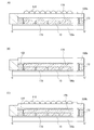
そこで、発明者は、複数の有機EL素子(以下、単に発光素子と記す)が直列に接続された発光ユニットが備える一方の発光素子の上部電極が、他方の発光素子の下部電極に接続する接続部の構成と、不良の発生原因となるメタルマスクに着眼した。そして、メタルマスクを用いることなく複数のEL層と複数の上部電極を形成し、第1の発光素子の上部電極が、第2の発光素子の下部電極に接続する構成、具体的には、第1の発光素子の下部電極の端部を覆う第1の隔壁を設け、第2の発光素子の下部電極上に、脚部及び脚部より投影面積が広くなるように電極上にせり出した台部を備える分離層と、分離層の一方の側に接する第2の隔壁とを設け、さらにメタルマスクを用いることなく形成された、発光性の有機化合物を含む層とそれに重ねて第1の発光素子の上部電極と第2の発光素子の上部電極とを有し、さらに第1の発光素子の上部電極が第1の隔壁を介して第1の発光素子の下部電極の端部と交差し、且つ分離層の台部と重なる領域において第2の発光素子の下部電極と電気的に接続する構成に想到し、上記課題の解決に至った。 Therefore, the inventor has a connection in which an upper electrode of one light emitting element provided in a light emitting unit in which a plurality of organic EL elements (hereinafter simply referred to as light emitting elements) are connected in series is connected to a lower electrode of the other light emitting element. Particular attention was paid to the structure of the part and the metal mask that would cause defects. A structure in which a plurality of EL layers and a plurality of upper electrodes are formed without using a metal mask, and the upper electrode of the first light emitting element is connected to the lower electrode of the second light emitting element, specifically, A first partition that covers an end portion of the lower electrode of the first light emitting element is provided, and a base portion that protrudes on the lower electrode of the second light emitting element so that a projected area is larger than the leg portion. And a second partition wall in contact with one side of the separation layer, a layer containing a light-emitting organic compound formed without using a metal mask, and a first light-emitting element superimposed on the layer And the upper electrode of the second light emitting element, the upper electrode of the first light emitting element intersects the end of the lower electrode of the first light emitting element through the first partition, and The second electrode of the second light emitting element is electrically connected to the base portion of the separation layer Conceive configured to connect, it led to solve the above problems.
これにより、第1の発光素子と第2の発光素子が直列に接続され、駆動電圧が高められた発光ユニットを提供することができる。また、メタルマスクを複数の上部電極の形成に使用しないため、前述した周辺部のボケの問題が生じない。このため、第1の発光素子の上部電極と、第2の発光素子の下部電極を精度よく接続することが可能となり、発光ユニットの開口率(発光ユニットの面積と、実際に発光する領域の面積の比)を高めることができる。 Accordingly, the light emitting unit in which the first light emitting element and the second light emitting element are connected in series and the driving voltage is increased can be provided. Further, since the metal mask is not used for forming the plurality of upper electrodes, the above-described problem of blurring in the peripheral portion does not occur. Therefore, the upper electrode of the first light-emitting element and the lower electrode of the second light-emitting element can be accurately connected, and the aperture ratio of the light-emitting unit (the area of the light-emitting unit and the area of the region that actually emits light) Ratio) can be increased.
加えて、第1の隔壁を設けることで、第1の電極の端部に生じる段差部における第1の電極と第2の電極の短絡を防止でき、さらに第2の隔壁を設けることで、分離層の台部と重なる領域における第3の電極と第4の電極の短絡を防止できる。 In addition, by providing the first partition wall, it is possible to prevent the first electrode and the second electrode from being short-circuited at the stepped portion generated at the end portion of the first electrode, and by providing the second partition wall, separation is achieved. It is possible to prevent a short circuit between the third electrode and the fourth electrode in a region overlapping with the base portion of the layer.
加えて、メタルマスクを用いずに複数のEL層と複数の上部電極を作製可能な構成とすることで、メタルマスクの開口端が基板表面を傷つけてしまうことによる不具合を防止でき、信頼性の高い発光ユニットを提供することができる。さらに、不要としたメタルマスクの作製費用並びに洗浄等の保守費用を削減する効果も奏する。 In addition, by adopting a configuration in which a plurality of EL layers and a plurality of upper electrodes can be manufactured without using a metal mask, it is possible to prevent problems caused by the opening end of the metal mask damaging the substrate surface, and reliability. A high light emitting unit can be provided. Furthermore, the production cost of unnecessary metal masks and maintenance costs such as cleaning can be reduced.
また、有機EL素子が有する下部電極や上部電極に接するEL層の一部に有機化合物と金属酸化物を含む複合材料を用いることで有機EL素子のエネルギーの損失を低減させ、発光効率の優れた有機EL素子を実現することができる。加えて、上記複合材料にハロゲン元素を添加することで、複合材料の抵抗率を低減することが可能となり、電圧降下による発光面内の輝度ばらつきを低減することができる。 In addition, by using a composite material containing an organic compound and a metal oxide for a part of the EL layer in contact with the lower electrode or the upper electrode of the organic EL element, energy loss of the organic EL element is reduced, and light emission efficiency is excellent. An organic EL element can be realized. In addition, by adding a halogen element to the composite material, it is possible to reduce the resistivity of the composite material, and it is possible to reduce luminance variations in the light-emitting surface due to a voltage drop.
有機化合物と金属酸化物を含む複合材料は、配線や電極として用いることもできる。また、配線や電極として、ハロゲン元素を含む上記複合材料を用いることもできる。また、配線や電極として、上記複合材料と、金属材料および/または透光性を有する導電性材料の積層を用いることもできる。 A composite material containing an organic compound and a metal oxide can also be used as a wiring or an electrode. Alternatively, the above-described composite material containing a halogen element can be used for the wiring and the electrode. Alternatively, a stack of the composite material, a metal material, and / or a light-transmitting conductive material can be used as a wiring or an electrode.
上部電極の抵抗値を下げることで、第1の発光素子の上部電極と、第2の発光素子の下部電極の接触面積を小さくすることができるため、発光ユニットの開口率を向上させることができる。 By reducing the resistance value of the upper electrode, the contact area between the upper electrode of the first light emitting element and the lower electrode of the second light emitting element can be reduced, so that the aperture ratio of the light emitting unit can be improved. .
上記複合材料に含まれる有機化合物には、正孔輸送性の高い有機化合物を用いることができる。また、上記金属酸化物には、酸化バナジウム、酸化ニオブ、酸化タンタル、酸化クロム、酸化モリブデン、酸化タングステン、酸化マンガン、酸化レニウムなどを用いることができる。特に、酸化モリブデンは大気中でも安定であり、吸湿性が低く、扱いやすいため好ましい。さらに、三酸化モリブデンを用いることが好ましい。また、上記複合材料としては、例えば、NPBと三酸化モリブデンとを含む複合材料を用いることができる。 As the organic compound contained in the composite material, an organic compound having a high hole-transport property can be used. As the metal oxide, vanadium oxide, niobium oxide, tantalum oxide, chromium oxide, molybdenum oxide, tungsten oxide, manganese oxide, rhenium oxide, or the like can be used. In particular, molybdenum oxide is preferable because it is stable in the air, has a low hygroscopic property, and is easy to handle. Furthermore, it is preferable to use molybdenum trioxide. As the composite material, for example, a composite material containing NPB and molybdenum trioxide can be used.
なお、本明細書において、第1の発光素子の下部電極を第1の電極、上部電極を第2の電極とも記す。また、第2の発光素子の下部電極を第3の電極、上部電極を第4の電極とも記す。 Note that in this specification, the lower electrode of the first light-emitting element is also referred to as a first electrode, and the upper electrode is also referred to as a second electrode. The lower electrode of the second light-emitting element is also referred to as a third electrode, and the upper electrode is also referred to as a fourth electrode.
本発明の一態様は、第1の電極と、第1の電極と重畳する第2の電極と、第1の電極の端部を覆う第1の隔壁を有し、第1の電極と第2の電極の間に形成された発光性の有機化合物を含む層を備える第1の発光素子と、第3の電極と、第3の電極上に形成された第2の隔壁と、第3の電極及び第2の隔壁上に形成された分離層と、第3の電極と重畳する第4の電極と、第3の電極と第4の電極の間に形成された発光性の有機化合物を含む層を備える第2の発光素子を有し、第2の電極と第3の電極は電気的に接続され、第2の電極と前記第4の電極は、有機化合物と金属酸化物を含む複合材料を有することを特徴とする発光ユニットである。 One embodiment of the present invention includes a first electrode, a second electrode overlapping with the first electrode, a first partition wall that covers an end portion of the first electrode, and the first electrode and the second electrode A first light-emitting element including a layer containing a light-emitting organic compound formed between the electrodes, a third electrode, a second partition formed on the third electrode, and a third electrode And a separation layer formed on the second partition, a fourth electrode overlapping with the third electrode, and a layer containing a light-emitting organic compound formed between the third electrode and the fourth electrode The second electrode and the third electrode are electrically connected, and the second electrode and the fourth electrode are made of a composite material containing an organic compound and a metal oxide. It is a light emitting unit characterized by having.
なお、本明細書中で示す発光素子は、トップエミッション構造である。したがって、第2の電極は発光性の有機化合物が発する光に対して透光性を有する。ただし、本発明はボトムエミッション構造やデュアルエミッション構造に適用することができる。ボトムエミッション構造の場合は、第1の電極が、発光性の有機化合物が発する光に対して透光性を有する。デュアルエミッション構造の場合は、第1の電極及び第2の電極が、発光性の有機化合物が発する光に対して透光性を有する。 Note that the light-emitting element described in this specification has a top-emission structure. Therefore, the second electrode has a light-transmitting property with respect to light emitted from the light-emitting organic compound. However, the present invention can be applied to a bottom emission structure or a dual emission structure. In the case of the bottom emission structure, the first electrode has a light-transmitting property with respect to light emitted from the light-emitting organic compound. In the case of a dual emission structure, the first electrode and the second electrode have a light-transmitting property with respect to light emitted from the light-emitting organic compound.
エネルギーの損失が少ない発光ユニットを提供することができる。または、信頼性の高い発光ユニットを提供することができる。または、開口率の高い発光ユニットを提供することができる。または、発光面内の輝度ばらつきが少ない発光ユニットを提供することができる。 A light-emitting unit with little energy loss can be provided. Alternatively, a highly reliable light-emitting unit can be provided. Alternatively, a light-emitting unit with a high aperture ratio can be provided. Alternatively, it is possible to provide a light emitting unit with less luminance variation in the light emitting surface.
エネルギーの損失が少ない発光ユニットを備えた発光装置を提供することができる。または、信頼性の高い発光ユニットを備えた発光装置を提供することができる。または、開口率の高い発光ユニットを備えた発光装置を提供することができる。または、発光面内の輝度ばらつきが少ない発光ユニットを備えた発光装置を提供することができる。 A light-emitting device including a light-emitting unit with little energy loss can be provided. Alternatively, a light-emitting device including a highly reliable light-emitting unit can be provided. Alternatively, a light-emitting device including a light-emitting unit with a high aperture ratio can be provided. Alternatively, a light-emitting device including a light-emitting unit with little luminance variation in the light-emitting surface can be provided.
エネルギーの損失が少ない発光ユニットを備えた照明装置を提供することができる。または、信頼性の高い発光ユニットを備えた照明装置を提供することができる。または、開口率の高い発光ユニットを備えた照明装置を提供することができる。または、発光面内の輝度ばらつきが少ない発光ユニットを備えた照明装置を提供することができる。 A lighting device including a light-emitting unit with little energy loss can be provided. Alternatively, a lighting device including a light-emitting unit with high reliability can be provided. Alternatively, a lighting device including a light-emitting unit with a high aperture ratio can be provided. Alternatively, it is possible to provide an illuminating device including a light emitting unit with little luminance variation in the light emitting surface.
エネルギーの損失が少ない発光ユニットの作製方法を提供することができる。または、信頼性の高い発光ユニットの作製方法を提供することができる。または、開口率の高い発光ユニットの作製方法を提供することができる。または、発光面内の輝度ばらつきが少ない発光ユニットの作製方法を提供することができる。 A method for manufacturing a light-emitting unit with low energy loss can be provided. Alternatively, a method for manufacturing a light-emitting unit with high reliability can be provided. Alternatively, a method for manufacturing a light-emitting unit with a high aperture ratio can be provided. Alternatively, a method for manufacturing a light-emitting unit with less luminance variation in the light-emitting surface can be provided.
本発明の実施の形態の一例について、図面を用いて以下に説明する。但し、本発明は以下の説明に限定されず、本発明の趣旨およびその範囲から逸脱することなくその形態および詳細を様々に変更し得ることは当業者であれば容易に理解される。従って、本発明は以下に示す実施の形態の記載内容に限定して解釈されるものではない。 An example of an embodiment of the present invention will be described below with reference to the drawings. However, the present invention is not limited to the following description, and it is easily understood by those skilled in the art that modes and details can be variously changed without departing from the spirit and scope of the present invention. Therefore, the present invention should not be construed as being limited to the description of the embodiments below.
図面等において示す各構成の、位置、大きさ、範囲などは、理解の簡単のため、実際の位置、大きさ、範囲などを表していない場合がある。このため、開示する発明は、必ずしも、図面等に開示された位置、大きさ、範囲などに限定されない。なお、実施の形態を説明するための全図において、同一部分又は同様な機能を有する部分には同一の符号を付し、その繰り返しの説明は省略する。 The position, size, range, and the like of each component illustrated in the drawings and the like may not represent the actual position, size, range, or the like for easy understanding. Therefore, the disclosed invention is not necessarily limited to the position, size, range, or the like disclosed in the drawings and the like. Note that in all the drawings for describing the embodiments, the same portions or portions having similar functions are denoted by the same reference numerals, and repetitive description thereof is omitted.
なお、本明細書等における「第1」、「第2」、「第3」などの序数は、構成要素の混同を避けるために付すものであり、数的に限定するものではない。 Note that ordinal numbers such as “first”, “second”, and “third” in this specification and the like are given to avoid confusion between components, and are not limited numerically.
(実施の形態1)
本実施の形態では、本発明の一態様の発光ユニットについて図1乃至図5を用いて説明する。
(Embodiment 1)
In this embodiment, a light-emitting unit of one embodiment of the present invention will be described with reference to FIGS.
≪構成例≫
まず、本実施の形態で示す発光ユニットの構成について図1及び図2を用いて説明する。なお、本実施の形態では、3つ発光素子を直列に接続した発光ユニットを例示するが、接続する発光素子の数はこれに限定されない。
≪Configuration example≫
First, the structure of the light-emitting unit described in this embodiment will be described with reference to FIGS. Note that although a light emitting unit in which three light emitting elements are connected in series is illustrated in this embodiment, the number of light emitting elements to be connected is not limited to this.
<構成例1>
図1(A)は、発光ユニットの上面図であり、図1(B)は、図1(A)におけるA−A’間の断面図である。なお、図面をわかりやすくするため、図1(A)では全面に形成される平坦化層134、EL層102(EL層102a乃至EL層102c)、上部電極108(上部電極108a乃至上部電極108c)、封止膜138の記載を省略している。また、図2(A)は、図1(A)におけるB−B’間の断面図である。また、図2(B)は、図1(A)におけるC−C’間の断面図である。図1(A)(B)及び図2(A)(B)に示す発光ユニットは、基板100上に、配線133a、配線133b、平坦化層134、隔壁107、第1の発光素子11、第2の発光素子12、第3の発光素子13、分離層139(脚部139a及び台部139b)、封止膜138a、及び封止膜138bを有する。
<Configuration example 1>
1A is a top view of the light emitting unit, and FIG. 1B is a cross-sectional view taken along the line AA ′ in FIG. Note that in order to make the drawing easy to understand, in FIG. 1A, a
第1の発光素子11は、隔壁107に形成された開口部109と重畳し、平坦化層134上に形成された下部電極103aと、下部電極103a上に形成されたEL層102aと、EL層102a上に形成された上部電極108aとを備える。
The first
第2の発光素子12は、隔壁107に形成された開口部109と重畳し、平坦化層134上に形成された下部電極103bと、下部電極103b上に形成されたEL層102bと、EL層102b上に形成された上部電極108bとを備える。
The second
第3の発光素子13は、隔壁107に形成された開口部109と重畳し、平坦化層134上に形成された下部電極103cと、下部電極103c上に形成されたEL層102cと、EL層102c上に形成された上部電極108cとを備える。
The third
第1の発光素子11において、下部電極103aは、配線133aと接続している。第3の発光素子13において、上部電極108cは、取り出し電極160を介して配線133bと接続している。
In the first light-emitting
構成例1では、下部電極103a乃至下部電極103cの端部に絶縁性の隔壁107が設けられている。上部電極108aは、該隔壁107を介して下部電極103aの端部と交差する。上部電極108aと下部電極103bとは、直接接続している。よって、第1の発光素子11と第2の発光素子12は、直列接続している。また、上部電極108bは、該隔壁107を介して下部電極103bの端部と交差する。上部電極108bと下部電極103cとは、直接接続している。よって、第2の発光素子12と第3の発光素子13は、直列接続している。また、上部電極108cは、該隔壁107を介して下部電極103cの端部と交差する。上部電極108cと電極160とは、直接接続している。
In Structural Example 1, an insulating
なお、隔壁107は順テーパー状の端部を有する。順テーパーとは、断面において、下地となる層に他の層がなだらかな角度で厚さを増して接する構成をいう。この時の角度をテーパー角という。言い換えると、テーパー角とは、テーパー形状を有する層(例えば、隔壁107)を、その断面(基板の表面と直交する面)に垂直な方向から観察した際に、当該層の側面と底面がなす傾斜角を示す。テーパー角が90°未満である場合を順テーパーといい、テーパー角が90°以上である場合を逆テーパーという。層の端部を順テーパー状とすることで、その上に形成する膜が途切れてしまう現象(段切れ)を防ぐことができる。
Note that the
上部電極108aが下部電極103bと接続する領域は、分離層139の台部139bが下部電極103b上にせり出した領域に含まれ、回り込みを抑制して成膜するEL層102bは下部電極103b上に形成されず、回り込みを促進して成膜する上部電極108aのみが下部電極103bに接して形成される。
The region where the
これにより、第1の発光素子11と第2の発光素子12が直列に接続され、駆動電圧が高められた発光ユニットを提供することができる。また、第2の発光素子12と第3の発光素子13に関しても同様のことが言える。
Thereby, the 1st
第1の発光素子11では、隔壁107が、下部電極103aの端部を覆うように設けられている。よって、下部電極103aの端部に生じる段差部における下部電極103aと上部電極108aの短絡を防止でき、信頼性の高い発光ユニットを提供することができる。さらに、下部電極103a上に隔壁を設けることで、台部139bと重なる領域における下部電極103aと上部電極108aの短絡を防止できる。また、第2の発光素子12と第3の発光素子13に関しても同様のことが言える。
In the first
構成例1では、ボイド141(空穴)を有する。ボイド141には、乾燥剤を導入させることがさらに好ましい。
In the configuration example 1, the void 141 (empty hole) is provided. More preferably, a desiccant is introduced into the
構成例1では、分離層139が、脚部139aと台部139bから形成されている。
また、分離層139は、脚部139aが下部電極103と隔壁107に接する領域の面積よりも、下部電極103に対する投影面積が広い台部139bを有している。すなわち、台部139bが、脚部139aが下部電極103と隔壁107に接する領域の外側にせり出して形成されている。
In the configuration example 1, the
Further, the
また、発光素子の上面を覆って封止膜138a及び封止膜138bを設けることで、信頼性の高い発光ユニットを実現することができる。
Further, by providing the
また、基板上に下地膜を設ける構成としても良い。封止膜や下地膜は、外部の水などから発光素子を保護する機能を有する。封止膜や下地膜を設けることで、発光素子の劣化を軽減し、発光ユニットの耐久性や寿命を向上させることができる。 Alternatively, a base film may be provided over the substrate. The sealing film and the base film have a function of protecting the light-emitting element from external water or the like. By providing the sealing film or the base film, deterioration of the light emitting element can be reduced and the durability and life of the light emitting unit can be improved.
〈下部電極の形状について〉
また、下部電極の一方の端部の形状を工夫することにより、下部電極と上部電極がEL層を介する構成であっても下部電極と上部電極との物理的、電気的接触を良好にすることができる。
<About the shape of the lower electrode>
In addition, by devising the shape of one end of the lower electrode, it is possible to improve the physical and electrical contact between the lower electrode and the upper electrode even if the lower electrode and the upper electrode are configured to have an EL layer interposed Can do.
図3に示す下部電極103の端部は、複数の段差形状を形成するように加工されている。このような段差形状を有する箇所では、比較的膜厚の小さいEL層102は段切れにより分断させることができる。一方、EL層102上に形成される上部電極108は、EL層102に比べて厚く形成することで、当該段差形状を分断することなく覆うことができる。したがって、EL層102が分断された段差形状の側面では、下部電極103と上部電極108とが直接接することが可能となり、電気的接触を良好にすることができる。
The ends of the
なお、図3には下部電極の端部の一領域に凹部を設ける形状としたが、例えば下部電極の端部をくし状の形状にするなど、EL層を効率的に分断させ、且つ上部電極が分断することなく覆うことの出来る形状を適宜設けることができる。 In FIG. 3, the concave portion is formed in one region of the end portion of the lower electrode. However, for example, the end portion of the lower electrode is comb-shaped, and the EL layer is efficiently divided and the upper electrode is formed. A shape that can be covered without being divided can be provided as appropriate.
<構成例2>
図6(A)は、構成例1と異なる構成を有する発光ユニットの断面図である。図6(A)に示す発光ユニットは、基板100上に、配線133a、平坦化層134、隔壁107、第1の発光素子11、第2の発光素子12、分離層139、封止膜138a、及び封止膜138bを有する。
<Configuration example 2>
6A is a cross-sectional view of a light-emitting unit having a configuration different from that of Configuration Example 1. FIG. A light-emitting unit illustrated in FIG. 6A includes a
構成例2は、構成例1と分離層139の構成が異なる。構成例1において、分離層139は、脚部139aと台部139bが異なる材料で形成されている構成としたが、構成例2で示す分離層139は、1種の材料で作製されている。なお、構成例2は、分離層139以外は、構成例1と同様の構成を有している。
In the configuration example 2, the configuration of the
<構成例3>
図6(B)は、構成例1及び構成例2と異なる構成を有する発光ユニットの断面図である。図6(B)に示す発光ユニットは、基板100上に、配線133a、平坦化層134、隔壁107、第1の発光素子11、第2の発光素子12、分離層139、封止膜138a、及び封止膜138bを有する。
<Configuration example 3>
FIG. 6B is a cross-sectional view of a light-emitting unit having a configuration different from Configuration Example 1 and Configuration Example 2. A light-emitting unit illustrated in FIG. 6B includes a
各発光素子は、平坦化層134上に形成された下部電極と、下部電極上に形成されたEL層と、EL層上に形成された上部電極とを備える。
Each light emitting element includes a lower electrode formed on the
構成例3は、構成例1及び構成例2と、隔壁107の構成が異なる。構成例3では、下部電極103aの端部と、下部電極103aの端部に隣接する下部電極103bの端部を覆うように隔壁107が設けられている。よって、下部電極103aの端部及び下部電極103bの端部に生じる段差部における下部電極103aと上部電極108aの短絡を防止でき、信頼性の高い発光ユニットを提供することができる。また、上部電極108aが薄い場合においても、下部電極103bの端部に生じる段差部で上部電極108aが段切れしにくくなり、信頼性の高い発光ユニットを提供することができる。
The configuration example 3 is different from the configuration examples 1 and 2 in the configuration of the
さらに、下部電極103b上に隔壁を設けることで、台部139bと重なる領域における下部電極103bと上部電極108bの短絡を防止できる。
Furthermore, by providing a partition wall on the
また、構成例1乃至構成例3にて説明した発光ユニットは、メタルマスクを用いずに複数のEL層と複数の上部電極を作製することができる。このため、メタルマスクの開口端が基板表面を傷つけてしまうことによる不具合を防止でき、信頼性の高い発光ユニットを提供することができる。さらに、不要としたメタルマスクの作製費用並びに洗浄費用を削減する効果も奏する。 The light-emitting units described in Structural Examples 1 to 3 can form a plurality of EL layers and a plurality of upper electrodes without using a metal mask. For this reason, the malfunction by the opening end of a metal mask damaging the substrate surface can be prevented, and a highly reliable light emitting unit can be provided. Furthermore, the production cost and cleaning cost of an unnecessary metal mask can be reduced.
≪材料≫
以下に、本発明の一態様である発光ユニットに用いることができる材料の一例を記す。
≪Material≫
Examples of materials that can be used for the light-emitting unit that is one embodiment of the present invention are described below.
[基板]
発光ユニットが有する発光素子の構造を、発光素子から放射する光を基板100側から取り出す構造(ボトムエミッション構造)とする場合に用いる基板100の材料としては、ガラス、石英、有機樹脂などの透光性を有する材料を挙げることができる。
[substrate]
As a material of the
例えば、基板100として有機樹脂を用いる場合、有機樹脂としては、例えば、ポリエチレンテレフタレート(PET)、ポリエチレンナフタレート(PEN)等のポリエステル樹脂、ポリアクリルニトリル樹脂、ポリイミド樹脂、ポリメチルメタクリレート樹脂、ポリカーボネート(PC)樹脂、ポリエーテルスルフォン(PES)樹脂、ポリアミド樹脂、シクロオレフィン樹脂、ポリスチレン樹脂、ポリアミドイミド樹脂、またはポリ塩化ビニル樹脂などを用いることができる。また、ガラス繊維に有機樹脂を含浸した基板や、無機フィラーを有機樹脂に混ぜた基板を使用することもできる。
For example, when an organic resin is used as the
また、発光素子の構造を、発光素子から放射する光を基板100が無い側から取り出す構造(トップエミッション構造)とする場合に用いる基板100の材料としては、上記材料の他にも遮光性を有する材料を用いることができる。例えば、アルミニウム、銅、鉄、ニッケル等や、ステンレス若しくはアルミニウム合金などの金属材料を挙げることができる。また、基板100として、シリコンやゲルマニウムなどの半導体基板を用いることも可能である。
In addition to the above materials, the light-emitting element has a light-shielding property as a material of the
特に、基板100に金属材料などの熱伝導性の良い材料を用いることで、発光素子に生じる熱を効率よく逃がすことができるため、発光ユニットの信頼性を高めることができる。すなわち、発光素子の構造をトップエミッション構造とすると、基板100に透光性基板を用いる必要がなくなるため、金属材料などの熱伝導性の良い材料を用いることができ、発光素子に生じる熱を効率よく逃がすことができる。また、配線133a及び配線133bと、基板100を直接接触させたくない場合は、配線133a及び配線133bと、基板100の間に絶縁膜を設ければよい。
In particular, by using a material having good thermal conductivity such as a metal material for the
[封止膜・下地膜]
封止膜・下地膜は、バリア性を有する材料を用いて形成することができる。
[Sealing film / Under film]
The sealing film and the base film can be formed using a material having a barrier property.
封止膜・下地膜としては、例えば、無機絶縁膜をスパッタリング法で形成することができる。例えば、窒化ケイ素膜、酸化アルミニウム膜、酸化ケイ素膜などを形成すれば良い。 As the sealing film / underlayer film, for example, an inorganic insulating film can be formed by a sputtering method. For example, a silicon nitride film, an aluminum oxide film, a silicon oxide film, or the like may be formed.
封止膜は、例えば水分の透過率が10−6g/m2・day以下程度のガスバリア性を備えるものが好ましい。また、封止膜の構成としては、例えば無機物を含む層を少なくとも一層、有機物を含む層の間に挟んで積層したものを用いることができる。有機物を含む層としては、例えばエポキシ系などの接着材層を一例として挙げることができ、無機物を含む層としては酸化珪素、窒化珪素などバリア性を有する膜を一例として挙げることができる。 The sealing film preferably has a gas barrier property with a moisture permeability of about 10 −6 g / m 2 · day or less. As the structure of the sealing film, for example, a layer in which at least one layer containing an inorganic substance is sandwiched between layers containing an organic substance can be used. As the layer containing an organic material, for example, an epoxy-based adhesive layer can be cited as an example, and as the layer containing an inorganic material, a film having a barrier property such as silicon oxide and silicon nitride can be cited as an example.
具体的には、支持体となるフィルムに数十μmの厚みで熱硬化性樹脂(例えば、エポキシ系接着剤)を塗布して乾燥し、その上に数μmの無機膜(例えば、酸化珪素膜)を成膜した第1部材に、離型フィルムに熱硬化性のエポキシを塗布して乾燥した第2の部材を貼り合わせて積層体を構成する。次いで、離型フィルムを剥がした該積層体の表面を上述の発光素子の上面に向かい合わせて貼り合わせ、熱圧着したのちエポキシ樹脂を熱硬化すればよい。このような構成とすることで発光素子の劣化を軽減し、発光ユニットの耐久性や寿命を向上させることができる。 Specifically, a thermosetting resin (for example, epoxy adhesive) having a thickness of several tens of μm is applied to a film as a support and dried, and an inorganic film (for example, a silicon oxide film) having a thickness of several μm thereon. And a second member dried by applying a thermosetting epoxy to a release film to form a laminate. Next, the surface of the laminate from which the release film has been peeled is bonded to the upper surface of the light-emitting element described above, and after thermocompression bonding, the epoxy resin may be thermally cured. With such a structure, deterioration of the light emitting element can be reduced, and durability and life of the light emitting unit can be improved.
また、基板として有機樹脂を用いる場合には、下地膜として、25μm以上100μm以下の厚さのガラス層を用いても良い。ガラス層の厚さは、代表的には、45μm以上80μm以下である。有機樹脂基板とガラス層とを組み合わせることで水分又は不純物等が発光ユニットの外部から発光素子に含まれる有機化合物や金属材料に侵入することを抑制することができ、かつ発光ユニットの軽量化を実現することができる。 In the case where an organic resin is used as the substrate, a glass layer having a thickness of 25 μm to 100 μm may be used as the base film. The thickness of the glass layer is typically 45 μm or more and 80 μm or less. By combining the organic resin substrate and the glass layer, moisture or impurities can be prevented from entering the organic compound or metal material contained in the light-emitting element from the outside of the light-emitting unit, and the light-emitting unit can be reduced in weight. can do.
[分離層]
分離層は、無機絶縁材料や有機絶縁材料を用いて形成することができる。例えば、ネガ型の感光性を有する樹脂材料を用いることができる。
[Separation layer]
The separation layer can be formed using an inorganic insulating material or an organic insulating material. For example, a negative photosensitive resin material can be used.
[発光素子] [Light emitting element]
下部電極は、光を取り出す側と反対側に設けられ、反射性を有する材料を用いて形成される。反射性を有する材料としては、アルミニウム、金、白金、銀、ニッケル、タングステン、クロム、モリブデン、鉄、コバルト、銅、又はパラジウム等の金属材料を用いることができる。そのほか、アルミニウムとチタンの合金、アルミニウムとニッケルの合金、アルミニウムとネオジムの合金などのアルミニウムを含む合金(アルミニウム合金)や銀と銅の合金などの銀を含む合金を用いることもできる。銀と銅の合金は、耐熱性が高いため好ましい。さらに、アルミニウム合金膜に接する金属膜、又は金属酸化物膜を積層することでアルミニウム合金膜の酸化を抑制することができる。該金属膜、金属酸化物膜の材料としては、チタン、酸化チタンなどが挙げられる。 The lower electrode is provided on the side opposite to the light extraction side, and is formed using a reflective material. As the reflective material, a metal material such as aluminum, gold, platinum, silver, nickel, tungsten, chromium, molybdenum, iron, cobalt, copper, or palladium can be used. In addition, an alloy containing aluminum (aluminum alloy) such as an alloy of aluminum and titanium, an alloy of aluminum and nickel, an alloy of aluminum and neodymium, or an alloy containing silver such as an alloy of silver and copper can be used. An alloy of silver and copper is preferable because of its high heat resistance. Furthermore, the oxidation of the aluminum alloy film can be suppressed by stacking a metal film or a metal oxide film in contact with the aluminum alloy film. Examples of the material for the metal film and metal oxide film include titanium and titanium oxide.
EL層は、少なくとも発光性の有機化合物を含む層を有する。そのほか、電子輸送性の高い物質を含む層、正孔輸送性の高い物質を含む層、電子注入性の高い物質を含む層、正孔注入性の高い物質を含む層、バイポーラ性の物質(電子輸送性及び正孔輸送性が高い物質)を含む層等を適宜組み合わせた積層構造を構成することができる。 The EL layer includes at least a layer containing a light-emitting organic compound. In addition, a layer containing a substance having a high electron transporting property, a layer containing a substance having a high hole transporting property, a layer containing a substance having a high electron injecting property, a layer containing a substance having a high hole injecting property, a bipolar substance (electron A stacked structure in which layers including a substance having a high transportability and a high hole-transport property are combined as appropriate can be formed.
また、本発明の一態様では、下部電極と上部電極の間に、複数のEL層を積層した発光素子(タンデム型発光素子)を適用することができる。好ましくは、2から4層(特に3層)構造とする。なお、EL層の構成例は他の実施の形態で詳細に説明する。 In one embodiment of the present invention, a light-emitting element (tandem light-emitting element) in which a plurality of EL layers is stacked between a lower electrode and an upper electrode can be used. A 2 to 4 layer (particularly 3 layer) structure is preferable. Note that a structure example of the EL layer will be described in detail in another embodiment.
上部電極に用いることができる透光性を有する導電性材料としては、酸化インジウム、酸化インジウム酸化スズ合金(ITO)、酸化インジウム酸化亜鉛合金、酸化亜鉛、ガリウムを添加した酸化亜鉛、グラフェンなどを用いることができる。 As a light-transmitting conductive material that can be used for the upper electrode, indium oxide, indium tin oxide alloy (ITO), indium zinc oxide alloy, zinc oxide, zinc oxide added with gallium, graphene, or the like is used. be able to.
また、上部電極として、金、白金、ニッケル、タングステン、クロム、モリブデン、鉄、コバルト、銅、パラジウム、又はチタン等の金属材料を用いることができる。または、それら金属材料の窒化物(例えば、窒化チタン)や酸化物を含む材料を用いてもよい。なお、金属材料(又はその窒化物や酸化物を含む材料)を用いる場合、透光性を有する程度に薄くすればよい。また、グラフェンを用いることもできる。 As the upper electrode, a metal material such as gold, platinum, nickel, tungsten, chromium, molybdenum, iron, cobalt, copper, palladium, or titanium can be used. Alternatively, a material containing a nitride (eg, titanium nitride) or oxide of the metal material may be used. Note that in the case where a metal material (or a material including a nitride or an oxide thereof) is used, the metal material may be thin enough to have a light-transmitting property. Graphene can also be used.
上部電極の膜厚は、例えば50nm以上300nm以下であり、好ましくは80nm以上130nm以下、さらに好ましくは100nm以上110nm以下である。 The film thickness of the upper electrode is, for example, 50 nm to 300 nm, preferably 80 nm to 130 nm, and more preferably 100 nm to 110 nm.
[配線]
配線の材料としては、銅(Cu)、チタン(Ti)、タンタル(Ta)、タングステン(W)、モリブデン(Mo)、クロム(Cr)、ネオジム(Nd)、スカンジウム(Sc)、ニッケル(Ni)、から選ばれた材料又はこれらを主成分とする合金材料を用いて、単層で又は積層して形成する。また、配線の材料としてアルミニウムを用いることもできるが、アルミニウムと、ITOなどの金属酸化物導電膜を直接接して設けると、アルミニウムが酸化されて抵抗値が増大する恐れがある。よって、配線を積層構造とし、ITOなどと接しない層にアルミニウムを用いればよい。本実施の形態の配線は、チタン膜上に銅膜を積層する構成とした。銅は抵抗が低いため、好適に用いることができる。配線の膜厚は、2μm以上35μm以下とすることが好ましい。
[wiring]
As wiring materials, copper (Cu), titanium (Ti), tantalum (Ta), tungsten (W), molybdenum (Mo), chromium (Cr), neodymium (Nd), scandium (Sc), nickel (Ni) , Or an alloy material containing these as a main component, and a single layer or a stacked layer. Aluminum can also be used as a material for the wiring. However, if aluminum and a metal oxide conductive film such as ITO are provided in direct contact with each other, aluminum may be oxidized to increase the resistance value. Therefore, the wiring may have a stacked structure, and aluminum may be used for a layer that is not in contact with ITO or the like. The wiring of this embodiment has a structure in which a copper film is stacked on a titanium film. Since copper has low resistance, it can be suitably used. The thickness of the wiring is preferably 2 μm or more and 35 μm or less.
[平坦化層]
平坦化層134は、無機絶縁材料又は有機絶縁材料を用いて形成することができる。なお、アクリル樹脂、ポリイミド、ベンゾシクロブテン系樹脂、ポリアミド、エポキシ樹脂等の、耐熱性を有する有機絶縁材料を用いると、平坦化絶縁膜として好適である。また上記有機絶縁材料の他に、低誘電率材料(low−k材料)、シロキサン系樹脂、PSG(リンガラス)、BPSG(リンボロンガラス)等を用いることができる。なお、これらの材料で形成される絶縁膜を複数積層させることで、平坦化層134を形成してもよい。
[Planarization layer]
The
平坦化層134の形成法は、特に限定されず、その材料に応じて、スパッタリング法、スピンコート法、ディッピング法、印刷法、インクジェット法等を用いることができる。
The formation method of the
[隔壁]
隔壁の材料としては、例えば、ポリイミド、アクリル樹脂、ポリアミド、エポキシ樹脂等の有機樹脂、または無機絶縁材料を用いることができる。
[Partition wall]
As a material for the partition wall, for example, an organic resin such as polyimide, acrylic resin, polyamide, or epoxy resin, or an inorganic insulating material can be used.
隔壁端部のテーパー角は、10度以上85度以下、好ましくは60度以上80度以下とするとよい。特に感光性の樹脂材料を用い、下部電極上に開口部109を形成し、その開口部の側壁が連続した曲率を持って形成される傾斜面となるように形成することが好ましい。具体的には、絶縁膜の断面が描いている曲線の曲率半径が、0.2μm以上2μm以下であることが望ましい。
The taper angle of the partition wall end is 10 degrees to 85 degrees, preferably 60 degrees to 80 degrees. In particular, it is preferable to use a photosensitive resin material and form the
隔壁の形成方法は、特に限定されないが、スパッタ法、蒸着法、液滴吐出法(インクジェット法)、印刷法(スクリーン印刷、オフセット印刷等)などを用いればよい。 A method for forming the partition wall is not particularly limited, and a sputtering method, a vapor deposition method, a droplet discharge method (inkjet method), a printing method (screen printing, offset printing, or the like) may be used.
隔壁の膜厚としては、例えば、20nm以上200nm以下とすれば良い。好ましくは、50nm以上100nm以下である。 The thickness of the partition wall may be, for example, 20 nm or more and 200 nm or less. Preferably, it is 50 nm or more and 100 nm or less.
本実施の形態は、他の実施の形態と自由に組み合わせることができる。 This embodiment can be freely combined with any of the other embodiments.
(実施の形態2)
本実施の形態では、先の実施の形態に示した本発明の一態様である発光ユニットの作製方法について、図4に示す断面図を用いて説明する。なお明瞭化のため、図4には図1で示した直列接続された複数の発光素子のうち、隣接する2つの発光素子を抜き出して示し、説明を行う。また、分離層139として用いることの出来る形状について、図5を用いて説明する。
(Embodiment 2)
In this embodiment, a method for manufacturing a light-emitting unit which is one embodiment of the present invention described in the above embodiment will be described with reference to cross-sectional views shown in FIGS. For the sake of clarity, FIG. 4 illustrates two adjacent light emitting elements extracted from the plurality of light emitting elements connected in series shown in FIG. A shape that can be used as the
<構成例1>
まず、基板100上に配線を構成する導電膜を形成する。当該導電膜は、スパッタリング法等の成膜方法を用いることができる。その後、公知の半導体加工技術を用いて不要な部分を除去し、配線133a、及び図4に図示しない配線133b(図1参照)を形成する。
<Configuration example 1>
First, a conductive film that forms a wiring is formed over the
次に、配線133a、配線133bを覆う平坦化層134を形成する。平坦化層134の形成法は、特に限定されず、その材料に応じて、スパッタ法、SOG法、スピンコート、ディップ、スプレー塗布、液滴吐出法(インクジェット法)、印刷法(スクリーン印刷、オフセット印刷等)等を用いることができる。その後、配線133a、配線133bのそれぞれに達する開口135を形成する。
Next, a
続いて、上記開口部を介して配線133a及び配線133bと接する導電膜を形成したのち、公知の半導体加工技術を用いて下部電極103a、下部電極103b、及び図4に図示しない取り出し電極160(図1参照)を形成する。
Subsequently, after forming a conductive film in contact with the
その後、下部電極103a、下部電極103bにおいて、これらの一方の端部を覆う隔壁107と、下部電極103a、及び103b上の隔壁107を同時に形成する(図4(A))。
After that, in the
続いて、下部電極103a、下部電極103b上に分離層139を形成する。
Subsequently, a
分離層139は、脚部139a、及び台部139bから構成される。また、分離層139は、脚部139aが下部電極103bと下部電極103b上に形成された隔壁107に接する領域の面積よりも、台部139bを下部電極103b上に投影した領域の面積が大きくなるように形成する。また、この加工を行う際、一度のパターニング工程で形成することが好ましい。
The
まず、後の脚部139aとなる絶縁膜149aと、後の台部139bとなる絶縁膜149bとを順に形成する(図4(B))。
First, an insulating
本実施の形態では、絶縁膜149a、絶縁膜149bは共にネガ型の感光性を有する有機樹脂膜を用いる。また、絶縁膜149aは、絶縁膜149bよりも露光に用いる光に対する感光性が低い材料を用いる。この感光性の違いは、これらに同じ強度の光を照射した場合、感光性の低い絶縁膜149aは、絶縁膜149bよりもパターン径が小さくなることを意味する。
In this embodiment mode, both the insulating
絶縁膜149a及び絶縁膜149bを形成した後、選択的に光を照射する。その後、現像処理を行うことにより、脚部139a及び台部139bを有する分離層139が形成される(図4(C))。この際、分離層139は、上記感光性の違いにより、台部139bを投影した面積に対し、脚部139aが下部電極103b及び下部電極103b上に形成された隔壁107に接する領域の面積が小さい形状となる。
After the insulating
なお、露光処理は複数回行ってもよく、例えば異なる2種類の波長を用いて2度の露光処理を行っても良い。 Note that the exposure process may be performed a plurality of times, for example, the exposure process may be performed twice using two different wavelengths.
次に、EL層及び上部電極となる導電層を成膜する。このとき、成膜されるEL層及び導電層の一部が分離層139によって物理的に分断されることにより、電気的に分離されたEL層102a、102bと、電気的に分離された上部電極108a、108bが形成される(図4(D))。すなわち、メタルマスクを用いなくとも、基板上に複数のEL層と複数の上部電極を作製することが可能となる。
Next, a conductive layer to be an EL layer and an upper electrode is formed. At this time, a part of the EL layer and the conductive layer to be formed are physically separated by the
また、上部電極の成膜は、分離層139のせり出した部分である台部139bの直下に回りこむように成膜し、直前に成膜されるEL層を覆うように成膜する。このように成膜することにより、上部電極の一端はEL層を乗り越え、台部139bと重畳する領域で下部電極と接することにより電気的に接続される。また上部電極の他の一端は、台部139bと重畳する隔壁107に接して形成される。
In addition, the upper electrode is formed so as to wrap around the
EL層の成膜方法としては、蒸着法等を用いることができる。また、上部電極の成膜方法としては、蒸着法、スパッタリング法等を用いることができる。スパッタリング法には例えばマグネトロンスパッタリング法のほかに、ミラートロンスパッタリング法を適用すると、回り込みを大きくすることができ好適である。 An evaporation method or the like can be used as a method for forming the EL layer. As a method for forming the upper electrode, a vapor deposition method, a sputtering method, or the like can be used. For example, in addition to the magnetron sputtering method, a mirrortron sputtering method is preferably used as the sputtering method because the wraparound can be increased.
上記のようにEL層を覆うように上部電極を形成する方法としては、成膜源と基板との距離を適宜設定することが挙げられる。例えば、成膜源と基板との距離を大きくとると台部139bのせり出した領域下への回り込みを小さくすることができ、一方この距離を小さくすることにより、台部139bのせり出した領域下への回りこみを大きくすることができる。したがって、EL層の形成では回り込みが小さくなるように成膜源と基板との距離を大きく設定し、一方上部電極の形成は、成膜源と基板との距離を小さく設定することにより形成することができる。
As a method of forming the upper electrode so as to cover the EL layer as described above, the distance between the film formation source and the substrate can be set as appropriate. For example, when the distance between the film forming source and the substrate is increased, the wraparound under the protruding area of the
以上により、基板100上に直列に接続された第1の発光素子11及び第2の発光素子12を形成することができる。
Through the above steps, the first light-emitting
続いて、基板100上の構造物全体を包み込むように覆う封止膜138a、138bを形成する(図4(E))。封止膜138aには、水分などの発光素子の劣化原因に繋がる不純物に対してバリア性を有する膜を用いることができる。例えば、スパッタリング法により形成される無機絶縁膜を用いることができる。
Subsequently, sealing
封止膜138aを形成すると、分離層139の台部139bのせり出した部分の直下に、ボイド141が形成される場合がある。しかし、封止膜138aを基板100上の構造物全体を包み込むように覆って形成するため、ボイド141は発光素子の信頼性になんら影響は及ぼさない。
When the
また、ボイド141には、乾燥剤を封入してもよい。例えば、封止膜138aを形成する前に、液滴吐出法等を用い、分離層139の台部139bのせり出して重なる領域下に乾燥剤を含む溶液を滴下、乾燥させることにより形成できる。ここで、用いる溶液の溶媒として水分を含まないことが好ましい。
In addition, a desiccant may be enclosed in the
また、封止膜138bは、上記実施の形態で例示した封止膜を適宜用いることができる。例えば、エポキシ樹脂を有するフィルムを基板100に貼り合わせ、熱圧着することにより形成することができる。
As the
なお、本実施の形態では、分離層139の形成方法として、感光性の異なる2種類の有機樹脂膜を用いる方法について説明したが、他の作製方法を適用することも出来る。
Note that although a method using two types of organic resin films with different photosensitivity is described as a method for forming the
例えば、絶縁膜149aとして無機絶縁膜を用い、絶縁膜149bとして感光性の有機膜を用いて形成することができる。まず露光、現像処理等を行い絶縁膜149bの不要な部分を除去し、台部139bを形成する。その後、台部139bをマスクとして用い、絶縁膜149aをエッチングすることにより脚部139aが形成される。このとき、形成される脚部139aは、下部電極103に対する投影面積が台部139bよりも小さくなるよう、エッチング時間等の条件を適宜調整する。また、絶縁膜149aのエッチングに用いる方法としては、露出する下部電極103や隔壁107へのエッチングによるダメージの小さい方法を用いることが好ましい。
For example, an inorganic insulating film can be used as the insulating
また、絶縁膜149aと絶縁膜149bとして、エッチング速度の異なる無機材料を組み合わせて用いることにより形成することもできる。代表的にはシリコン酸化膜とシリコン窒化膜の組み合わせが挙げられるが、これに限られず、シリコンやゲルマニウムを含む絶縁膜や、有機絶縁膜、金属酸化物絶縁膜等から選択された組み合わせを適宜用いることができる。まず、絶縁膜149b上にフォトリソグラフィ法によりレジストマスクを形成し、絶縁膜149aに対するエッチング速度の遅い条件で絶縁膜149bをエッチングすることにより、台部139bを形成した後、レジストマスクを除去する。その後、台部139bをマスクとして、台部139bを構成する膜に対するエッチング速度の遅い条件で絶縁膜149aをエッチングすることにより、脚部139aを形成する。レジストマスクの除去は、台部139bを形成した後でも、脚部139aを形成した後でもよく、レジストマスクを除去せずに残しておくこともできる。また、エッチングの方法については、上記と同様、下層へのエッチングによるダメージに配慮することが好ましい。
Alternatively, the insulating
また、絶縁膜149aと、絶縁膜149bに、それぞれ反対の感光性を有する有機樹脂膜を用いて形成してもよい。例えば、絶縁膜149aにポジ型の感光性を有する有機樹脂膜を用い、絶縁膜149bにネガ型の感光性を有する有機樹脂膜を用いて形成することができる。この場合、絶縁膜149aを成膜し、選択的に露光、現像、加熱処理等を行うことにより、脚部139aを形成し、続いて絶縁膜149bを成膜した後に、選択的に露光、現像、加熱処理等を行うことにより、台部139bを形成することで、分離層139を形成することができる。
Alternatively, the insulating
また、絶縁膜149aとして感光性の有機膜を用い、絶縁膜149bに無機絶縁膜を用いても良い。まず、絶縁膜149a及び絶縁膜149bの積層膜を形成し、フォトリソグラフィ法を用いて絶縁膜149bをエッチングして台部139bを形成する。続いて台部139bをハードマスクとして、絶縁膜149aを逆テーパー形状になるようエッチングすることにより、脚部139aを形成する。ここで絶縁膜149aのエッチングの際に、ドライエッチングを用いると、脚部139aの形状を制御しやすいため好ましい。
Alternatively, a photosensitive organic film may be used as the insulating
分離層139は、上記の作製方法に限らず、絶縁膜149a、絶縁膜149bとしてネガ型の感光性有機膜、ポジ型の感光性有機膜、無機絶縁膜等を組み合わせて適宜形成することができる。また、上記では分離層139が2層構造である場合を示したが、単層でも良いし、2層以上の多層構造とすることが出来る。
The
このように、分離層139は様々な作製方法により形成することができる。したがって、このような作製方法の違いにより、分離層139は異なる形状となる場合がある。以下、分離層139として用いることの出来る形状について図5を参照して説明する。
In this manner, the
図5(A)に示す分離層139は、異なる絶縁膜からなる脚部139aと、台部139bとを有する。脚部139a、及び台部139bの断面形状は、共に概略四辺形の形状を有し、台部139bの下部電極103に対する投影面積が、脚部139aが下部電極103と下部電極103b上に形成された隔壁107に接する面積よりも大きい特徴を有している。なお、台部139bの断面形状における上端の角は、丸みを帯びていても良い。また、図5(A)に示すように、脚部139aの上部は広がりを有していても良い。
The
図5(B)に示す分離層139は、単一の絶縁膜から構成されており、その断面は角柱の中ほどから底部にかけてくびれを設けたような形状を有している。また、その上部は、底部に対して水平方向にせり出した形状となっている。なお、上記と同様に、上端の角は丸みを帯びていても良い。
The
図5(C)に示す分離層139は、異なる絶縁膜からなる脚部139aと台部139bとを有する。脚部139a及び台部139bの断面形状は概略台形形状である。分離層139を上部から見たとき、脚部139aは、上部よりも底部の投影面積の方が大きく、一方、台部139bは、上部よりも底部の投影面積の方が小さい形状となっている。さらに、台部139bの上部の面積よりも、脚部139aの底部の面積が小さい特徴を有している。
The
ここで、図5(A)(B)(C)に示す分離層139は、以下のような共通の特徴を有している。図5(A)(B)(C)の破線に示すように、いずれの分離層139においても、分離層139の上部(又は台部)の先端と、分離層139の下部(脚部)側面が下部電極103と接する点を結んだ直線145よりも、脚部側に空間146を有する形状となっている。このようなくびれた部分を設けることにより、EL層の成膜時には回り込みを抑制した成膜方法を、また上部電極の成膜時には回り込みを促進した成膜方法を適用することが可能となり、上部電極と下部電極との電気的接続が容易になる。
Here, the
また、分離層139のテーパー角は、下部電極103の上面が接する分離層139の底面、または隔壁107の上面が接する分離層139の底面と、直線145がなす傾斜角αと見ることもできる。
The taper angle of the
上記実施の形態で例示した構成例1以外の他の構成例についても、構成例1と同様の作製方法をほぼ適用することが出来る。構成例1と異なる点を以下に挙げる。 A manufacturing method similar to that of the configuration example 1 can be almost applied to the configuration examples other than the configuration example 1 illustrated in the above embodiment. The differences from Configuration Example 1 are given below.
<構成例2>
構成例2(図6(A)参照)は、分離層139が構成例1と異なる。分離層139はネガ型の感光性を有する有機膜を形成し、露光、現像処理を行うことにより形成することができる。ここで、有機膜の下部に向かって露光強度が低下するよう露光強度を調整することにより、分離層139の下部への光の回りこみの影響が促進され、分離層139をいわゆる逆テーパー形状とすることが出来る。
<Configuration example 2>
In Configuration Example 2 (see FIG. 6A), the
<構成例3>
構成例3(図6(B)参照)は、隔壁107が、下部電極103aの端部と該端部に隣接する下部電極103bの端部を覆う点で構成例1と異なる。したがって、隔壁107を隣接する下部電極の端部を覆う形状となるように形成すればよい。
<Configuration example 3>
Configuration Example 3 (see FIG. 6B) differs from Configuration Example 1 in that the
本実施の形態の作製方法では、感度が異なる感光性樹脂を二種類積層された層を用い、選択的に露光し、現像して分離層139を形成する。また、回り込みを抑制してEL層102を成膜し、回り込みを促進して上部電極108を形成する。このような方法により、脚部139aより上部電極108上にせり出した台部139bを有する分離層139を容易に形成することができ、加えてメタルマスクを用いることなく、下部電極103と上部電極108の間にEL層102を形成し、且つ台部139bと重畳する領域において上部電極108と下部電極103(図6(B)においては、上部電極108aと下部電極103b)を電気的に接続できる。メタルマスクを用いずに複数のEL層と上部電極を作製する方法であるため、メタルマスクの開口端が基板表面を傷つけてしまうことによる不具合を防止でき、信頼性の高い発光ユニットを提供することができる。さらに、不要としたメタルマスクの作製費用並びに洗浄等の保守費用を削減する効果も奏する。
In the manufacturing method of this embodiment mode, a layer in which two types of photosensitive resins having different sensitivities are stacked is selectively exposed and developed to form the
本実施の形態は、他の実施の形態と自由に組み合わせることができる。 This embodiment can be freely combined with any of the other embodiments.
(実施の形態3)
本実施の形態では、本発明の一形態として上記実施の形態で例示した発光ユニットを適用した発光装置の一例について、図7及び図8を用いて説明する。
(Embodiment 3)
In this embodiment, an example of a light-emitting device to which the light-emitting unit exemplified in the above embodiment is applied as one embodiment of the present invention will be described with reference to FIGS.
図7(A)に、発光装置1000の構成の模式図を示す。発光装置1000は、コンバータ150と、複数の発光ユニット10を有する。複数の発光ユニット10はそれぞれ並列に接続し、それぞれの発光ユニット10には、コンバータ150に接続される配線133a、及び配線133bが接続される。
FIG. 7A illustrates a schematic diagram of a structure of the light-emitting
コンバータ150は、例えば、家庭用の交流電源から出力される電圧を直流電圧に変換するAC−DCコンバータや、入力された直流電圧と異なる大きさの直流電圧を出力するDC−DCコンバータなどを用いることができる。コンバータ150に接続される配線133a及び配線133bには、異なる電圧が出力される。配線133a及び配線133bに接続される発光ユニット10はこの電圧差により電流を流し、発光させることができる。
The
並列に接続される複数の発光ユニット10は、コンバータ150の出力特性に応じて、その数を適宜設定すればよい。コンバータ150の流すことの出来る電流が大きいほど、多くの発光ユニット10を並列に接続することができる。
The number of light emitting
次に、発光ユニット10の構成について図7(B)及び図7(C)を用いて説明する。図7(B)は、発光ユニット10の構成とそれらの接続関係を模式的に示した図であり、図7(C)は、発光ユニット10内の複数の発光素子の接続関係を示す等価回路である。
Next, the structure of the
図7(B)に示す発光ユニット10a、発光ユニット10b、及び発光ユニット10cは、それぞれ複数の発光素子1100を有し、配線133a及び配線133bに接続している。本実施の形態では、9個の発光素子1100が、行方向、列方向にマトリクス状に複数配置された構成の発光ユニット10について例示する。なお、発光ユニット10に設ける発光素子1100の数は、上記コンバータ150の出力特性や、発光装置1000のレイアウトなどによって適宜設定すればよい。
Each of the
それぞれの発光素子1100は上記実施の形態で例示した発光素子を適用することができ、それぞれ下部電極103、EL層102、及び上部電極108を有する。
Each light-emitting
発光ユニット10a乃至発光ユニット10cは、それぞれが行方向に直列に接続された複数の発光素子1100を有している。具体的には、行方向に配置された発光素子1100は、上部電極が隣接する発光素子1100の下部電極に接続され、これが繰り返されることにより、直列接続されている。発光素子1100は、上記実施の形態に例示した方法、構成を用いて接続することが出来る。また、発光ユニット10a乃至発光ユニット10cは、列方向に並列に接続されている。
Each of the
また、図7(B)には、2つの発光ユニット10を左右対称に設けた構成を示している。このような構成とすることにより、配線133a、及び配線133bのそれぞれの発光素子に接続する部分を共有して用いることができるため、発光ユニット10間のスペースを小さく出来、基板面積に対する発光面積を大きくすることができる。
FIG. 7B shows a configuration in which two light emitting
上記接続関係を示した等価回路を図7(C)に示す。このように直列に接続された発光素子1100の一群を並列に接続することにより、例えば発光ユニット10内の一つの発光素子1100がショートしてしまった場合でも、他の発光素子に流れる電流が遮断されること無く発光させることができる。
An equivalent circuit showing the connection relation is shown in FIG. By connecting a group of light emitting
本実施の形態では、直列に接続された発光素子の一群を並列接続する構成としたが、列方向に隣接する各発光素子間において、それぞれの発光素子の下部電極、又は上部電極を接続し、列方向に並列接続する構成としてもよい。このように、直列接続、並列接続を組み合わせた接続関係とすることにより、例えば発光ユニット10内の一つの発光素子1100がショート、若しくは絶縁化してしまったときでも、当該発光素子1100に隣接する他の発光素子1100に流れる電流が遮断されること無く、発光させることが可能となる。
In the present embodiment, a group of light emitting elements connected in series is configured to be connected in parallel, but between each light emitting element adjacent in the column direction, a lower electrode or an upper electrode of each light emitting element is connected, It may be configured to be connected in parallel in the column direction. In this way, by connecting the series connection and the parallel connection, for example, even when one
図8(A)及び図8(B)に、図7(A)におけるG−G’間の断面図を示す。 8A and 8B are cross-sectional views taken along the line G-G ′ in FIG.
図8(A)を用いて、基板として有機樹脂基板を用いた場合の発光装置の一例を説明する。図8(A)に示す発光装置は、第1の基板100a上に、第1のガラス層173aが形成され、第1のガラス層173a上に複数の発光ユニット10が設けられている。図8(A)において、第1のガラス層173a及び第2のガラス層173bは、シール材171で貼り合わされている。図8(A)に示す発光装置は、第1のガラス層173a、第2のガラス層173b及びシール材171で囲まれた空間175に発光ユニット10を備える構成となっている。また、第1の基板100a及び第2の基板100bは、シール材172で貼り合わされている。
An example of a light-emitting device in the case where an organic resin substrate is used as a substrate will be described with reference to FIG. In the light-emitting device illustrated in FIG. 8A, a
シール材171とシール材172との間には空間を設けても良い。また、シール材171とシール材172とが接していても良い。
A space may be provided between the sealing
なお、発光ユニット10を構成するEL層と上部電極となる導電層を成膜する際に、発光ユニット10が形成される領域は覆わず、シール材171及びシール材172が形成される領域を覆うメタルマスクを用いて、シール材171及びシール材172が形成される領域にEL層及び導電層が成膜されないようにしてもよい。
Note that, when the EL layer constituting the
上記発光装置において、第1の基板100a及び第2の基板100bは同じ有機樹脂材料からなることが好ましい。同じ材料で形成することで、熱歪みや物理的衝撃による形状不良を抑制することができる。よって、作製時及び使用時における発光装置の変形や破損などを抑制することができる。
In the light-emitting device, the
本発明の一態様の発光装置は、有機樹脂基板とガラス層とを用いる。よって、発光装置を軽量化できる。さらに、水分又は不純物等が発光装置の外部から発光ユニット10に含まれる有機化合物や金属材料に侵入することを抑制することができる。
The light-emitting device of one embodiment of the present invention uses an organic resin substrate and a glass layer. Therefore, the light emitting device can be reduced in weight. Furthermore, it is possible to prevent moisture, impurities, or the like from entering the organic compound or metal material contained in the
図8(B)を用いて、第1の基板100aとして金属基板、第2の基板100bとしてガラス基板を用いた場合の発光装置の一例を説明する。図8(B)に示す発光装置は、第1の基板100a上に絶縁膜178を介して複数の発光ユニット10が設けられている。図8(B)において、第1の基板100a及び第2の基板100bは、シール材172で貼り合わされている。
An example of a light-emitting device in the case where a metal substrate is used as the
第1の基板100aとして用いる金属基板の材料に特段の限定はないが、アルミニウム、銅、ニッケル等の金属、または、アルミニウム合金若しくはステンレスなどの金属の合金などを用いることができる。また、金属基板の膜厚に特段の限定はないが、例えば、10μm以上200μm以下のものを用いると、発光装置の軽量化が図れるため好ましい。
There is no particular limitation on the material of the metal substrate used for the
第1の基板100aとしては、金属基板のほかにも、ガラス基板や石英基板などを用いることができる。
As the
図8(A)に示すように、コンバータ150は上下の基板の間に設けることができる。また、図8(B)に示すように、第2の基板100bを第1の基板100aよりも小さくすることで、発光装置の厚みを変えずに厚みのあるコンバータを内蔵することができる。
As shown in FIG. 8A, the
空間175には、不活性気体(窒素、アルゴンなど)が充填されている(図8(A))。また、空間175内の、発光ユニット10の発光の妨げにならない領域に、乾燥剤を入れても良い。例えば、アルカリ土類金属の酸化物(酸化カルシウムや酸化バリウム等)のように、化学吸着によって水分を吸収する物質を用いることができる。その他の乾燥剤として、ゼオライトやシリカゲル等のように、物理吸着によって水分を吸着する物質を用いてもよい。
The
空間175を、透光性を有する充填材176で充填する構成とすることもできる(図8(B))。充填材176は、できるだけ水分や酸素を透過しない材料であることが望ましい。また、乾燥剤入りの充填材176を用いることもできる。
The
また、充填材176と発光ユニット10との間に保護膜を形成しても良い。保護膜を設けることで、充填材176からEL層に水分が侵入することを防ぐことができ、発光ユニット10の寿命の低下を抑制することができる。保護膜としては、例えば、窒化シリコン膜、窒化酸化シリコン膜、酸化アルミニウム膜、窒化アルミニウム膜等を用いることができる。
Further, a protective film may be formed between the
シール材171としては公知の材料を用いることができる。例えば、熱硬化型の材料、紫外線硬化型の材料を用いても良い。シール材171には、ガラス同士を接着することができる材料、シール材172には、有機樹脂同士を接着することができる材料を用いる。これらの材料はできるだけ水分や酸素を透過しない材料であることが望ましい。また、乾燥剤入りのシール材を用いることもできる。
A known material can be used as the sealing
本実施の形態は、他の実施の形態と自由に組み合わせることができる。 This embodiment can be freely combined with any of the other embodiments.
(実施の形態4)
本実施の形態では、上記実施の形態で例示した発光ユニット10を適用した発光装置の光取り出し効率を向上させる構成について、図9を用いて説明する。なお、図9は、図8(B)で説明した発光装置の光取り出し効率を向上させる例について示している。
(Embodiment 4)
In this embodiment, a structure for improving light extraction efficiency of a light-emitting device to which the light-emitting
一般に、有機EL素子を用いた発光装置は、光を発光装置の外(大気中)へ取り出すときに発光装置内、又は発光装置と大気との境界面で全反射が起こる条件があり、発光ユニット10の光取り出し効率は100%より小さいという問題がある。一般的には、発光ユニット10の光取り出し効率は、20%から30%程度と言われている。
In general, a light emitting device using an organic EL element has a condition that total reflection occurs inside the light emitting device or at the interface between the light emitting device and the atmosphere when light is taken out of the light emitting device (in the atmosphere). There is a problem that the light extraction efficiency of 10 is less than 100%. Generally, the light extraction efficiency of the
具体的には、屈折率の高い媒体Aから屈折率の低い媒体Bへ光が入射する際に、入射する角度により全反射することがある。 Specifically, when light enters from a medium A having a high refractive index into a medium B having a low refractive index, total reflection may occur depending on the incident angle.
このとき、媒体Aと媒体Bとの界面に凹凸の構造を設けることが好ましい。このような構成にすることで、媒体Aから媒体Bに臨界角を超えて入射する光が全反射し、光の取り出し効率が低下する現象を抑制することができる。 At this time, it is preferable to provide an uneven structure at the interface between the medium A and the medium B. With such a configuration, it is possible to suppress a phenomenon in which light incident from the medium A to the medium B exceeding the critical angle is totally reflected and the light extraction efficiency is lowered.
下記に記す本発明の一態様である発光装置の光取り出し効率は、本発明を適用していない発光装置の1.2倍から2倍程度にすることができる。 The light extraction efficiency of the light-emitting device which is one embodiment of the present invention described below can be about 1.2 to 2 times that of the light-emitting device to which the present invention is not applied.
<変形例1>
変形例1は、基板100bの大気と接する側の面に、凹凸形状を有する構造体118を有する以外は、実施の形態3に示した構成と同様の構成を適用することができる。
<
In the first modification, a configuration similar to the configuration described in Embodiment 3 can be applied except that the surface of the
基板100bの屈折率は大気の屈折率よりも大きいため、基板100bと大気との界面で全反射が起こることがある。変形例1では、大気と基板100bの界面に構造体118を設けているため、全反射の影響で大気中に取り出せない光を低減し、発光ユニット10の光の取り出し効率を向上させることができる。
Since the refractive index of the
構造体118は、ストライプ状であっても効果を奏するが、マトリクス状であることが好ましい。凹凸のパターンは、特に限定されず、例えば、円錐、角錐(三角錐、四角錐等)、傘状などの頂点を有する形状や、半球状とすることができる。
The
凹凸の大きさ、高さについては、0.1μm以上1000μm以下程度とすることが好ましい。特に、1μm以上であると、光の干渉による影響を抑制することができるため、好ましい。 About the magnitude | size and height of an unevenness | corrugation, it is preferable to set it as about 0.1 micrometer or more and 1000 micrometers or less. In particular, the thickness of 1 μm or more is preferable because the influence of light interference can be suppressed.
凹凸のパターンは、隣り合う部分において隙間が生じないように設けられていることが好ましい。例えば、パターンは最密充填で配置されることが好ましい。また、パターンは基板の大気と接する面全面又は一部に形成すれば良い。少なくとも発光領域に形成されていることが好ましい。 It is preferable that the uneven pattern is provided so that no gap is formed between adjacent portions. For example, the pattern is preferably arranged with close packing. The pattern may be formed on the entire surface or part of the surface of the substrate in contact with the atmosphere. It is preferably formed at least in the light emitting region.
構造体118は、基板100bの表面に、半球レンズ、マイクロレンズアレイや、凹凸形状を有する構造体118が施されたフィルム、光拡散フィルム等を、公知の接着剤等を用いて接着することで形成することができる。
The
また、基板100bに直接凹凸の構造を形成しても良い。基板に直接凹凸の構造を形成する方法としては、例えば、エッチング法、砥粒加工法(サンドブラスト法)、マイクロブラスト加工法、液滴吐出法や、印刷法(スクリーン印刷やオフセット印刷などパターンが形成される方法)、スピンコート法などの塗布法、ディッピング法、ディスペンサ法、ナノインプリント法等を適宜用いることができる。
Further, an uneven structure may be directly formed on the
本発明の一態様では、大気と接する面に構造体118を設けることで、全反射の影響で大気に取り出せない光を低減し、発光装置の光の取り出し効率を向上させることができる。
In one embodiment of the present invention, the
<変形例2>
次に、図9(A)と異なる構成を有する発光装置について、図9(B)及び図9(C)を用いて説明する。
<Modification 2>
Next, a light-emitting device having a structure different from that in FIG. 9A will be described with reference to FIGS. 9B and 9C.
実施の形態3で説明した図8(B)では、空間175を、透光性を有する充填材176で充填する構成を示した(図8参照)。このため、発光ユニット10から発せられた光は、充填材176を介して基板100bへ入射する際に全反射することがある。したがって、全反射が起こる条件がある界面に凹凸の構造体を設けることが好ましい。
FIG. 8B described in Embodiment 3 shows a structure in which the
変形例2で説明する発光ユニット10(図9(B))は、基板100bの発光ユニット10側に凹凸形状を有する構造体122を設ける。これら以外は、実施の形態3に示した構成と同様の構成を適用することができる。
In the light-emitting unit 10 (FIG. 9B) described in Modification 2, a
変形例2では、基板100bと充填材176の間に構造体122を設ける。よって、臨界角を超えて入射する光が全反射し、光の取り出し効率が低下する現象を抑制することができる。
In the second modification, the
なお、先の実施の形態で記した構造体118と組み合わせた構成の一例について、図9(C)に示す。構造体118と構造体122の両方を設けることで、光の取り出し効率をさらに高めることができる。
Note that an example of a structure combined with the
構造体122は、構造体118と同様に形成することができる。凹凸の大きさ、高さについては、0.1μm以上1000μm以下程度とすることが好ましい。特に、1μm以上であると、光の干渉による影響を抑制することができるため、好ましい。
The
また、凹凸の大きさによっては、凹凸のパターンに周期性があると、凹凸が回折格子のような働きをすることで、干渉効果が強くなり、特定の波長の光が大気に取り出されやすくなることがある。したがって、凹凸のパターンは周期性をもたないことが好ましい。また、パターンは少なくとも発光領域に形成されていれば良い。 In addition, depending on the size of the unevenness, if the uneven pattern has periodicity, the unevenness acts like a diffraction grating, which increases the interference effect and makes it easier to extract light of a specific wavelength to the atmosphere. Sometimes. Therefore, the uneven pattern preferably has no periodicity. Moreover, the pattern should just be formed in the light emission area | region at least.
本実施の形態では、凹凸の構造体を設けることで、臨界角を超えて入射する光が全反射し、発光ユニット10内を光が導波して光の取り出し効率が低下する現象を抑制することができる。
In the present embodiment, by providing an uneven structure, light that enters beyond the critical angle is totally reflected, and light is guided through the
本実施の形態は、他の実施の形態と自由に組み合わせることができる。 This embodiment can be freely combined with any of the other embodiments.
(実施の形態5)
本実施の形態では、本発明の一態様に適用できるEL層の一例について、図10を用いて説明する。
(Embodiment 5)
In this embodiment, an example of an EL layer that can be applied to one embodiment of the present invention will be described with reference to FIGS.
図10(A)に示すEL層102は、下部電極103と上部電極108の間に設けられている。下部電極103及び上部電極108は、実施の形態1と同様の構成を適用することができる。
The
本実施の形態において、EL層102は、下部電極103側から、電子注入層705、電子輸送層704、発光性の有機化合物を含む層703、正孔輸送層702、及び正孔注入層701、の順で積層されている。
In this embodiment, the
図10(A)に示す発光素子の作製方法について説明する。 A method for manufacturing the light-emitting element illustrated in FIG. 10A will be described.
正孔注入層701は、正孔注入性の高い物質を含む層である。正孔注入性の高い物質としては、例えば、酸化モリブデン、酸化チタン、酸化バナジウム、酸化レニウム、酸化ルテニウム、酸化クロム、酸化ジルコニウム、酸化ハフニウム、酸化タンタル、酸化銀、酸化タングステン、酸化マンガン等の金属酸化物を用いることができる。また、フタロシアニン(略称:H2Pc)、銅(II)フタロシアニン(略称:CuPc)等のフタロシアニン系の化合物を用いることができる。
The
また、低分子の有機化合物である4,4’,4’’−トリス(N,N−ジフェニルアミノ)トリフェニルアミン(略称:TDATA)、4,4’,4’’−トリス[N−(3−メチルフェニル)−N−フェニルアミノ]トリフェニルアミン(略称:MTDATA)、4,4’−ビス[N−(4−ジフェニルアミノフェニル)−N−フェニルアミノ]ビフェニル(略称:DPAB)、4,4’−ビス(N−{4−[N’−(3−メチルフェニル)−N’−フェニルアミノ]フェニル}−N−フェニルアミノ)ビフェニル(略称:DNTPD)、1,3,5−トリス[N−(4−ジフェニルアミノフェニル)−N−フェニルアミノ]ベンゼン(略称:DPA3B)、3−[N−(9−フェニルカルバゾール−3−イル)−N−フェニルアミノ]−9−フェニルカルバゾール(略称:PCzPCA1)、3,6−ビス[N−(9−フェニルカルバゾール−3−イル)−N−フェニルアミノ]−9−フェニルカルバゾール(略称:PCzPCA2)、3−[N−(1−ナフチル)−N−(9−フェニルカルバゾール−3−イル)アミノ]−9−フェニルカルバゾール(略称:PCzPCN1)等の芳香族アミン化合物等を用いることができる。 In addition, 4,4 ′, 4 ″ -tris (N, N-diphenylamino) triphenylamine (abbreviation: TDATA), 4,4 ′, 4 ″ -tris [N- ( 3-methylphenyl) -N-phenylamino] triphenylamine (abbreviation: MTDATA), 4,4′-bis [N- (4-diphenylaminophenyl) -N-phenylamino] biphenyl (abbreviation: DPAB), 4 , 4′-bis (N- {4- [N ′-(3-methylphenyl) -N′-phenylamino] phenyl} -N-phenylamino) biphenyl (abbreviation: DNTPD), 1,3,5-tris [N- (4-diphenylaminophenyl) -N-phenylamino] benzene (abbreviation: DPA3B), 3- [N- (9-phenylcarbazol-3-yl) -N-phenylamino]- -Phenylcarbazole (abbreviation: PCzPCA1), 3,6-bis [N- (9-phenylcarbazol-3-yl) -N-phenylamino] -9-phenylcarbazole (abbreviation: PCzPCA2), 3- [N- ( An aromatic amine compound such as 1-naphthyl) -N- (9-phenylcarbazol-3-yl) amino] -9-phenylcarbazole (abbreviation: PCzPCN1) can be used.
さらに、高分子化合物(オリゴマー、デンドリマー、ポリマー等)を用いることもできる。例えば、ポリ(N−ビニルカルバゾール)(略称:PVK)、ポリ(4−ビニルトリフェニルアミン)(略称:PVTPA)、ポリ[N−(4−{N’−[4−(4−ジフェニルアミノ)フェニル]フェニル−N’−フェニルアミノ}フェニル)メタクリルアミド](略称:PTPDMA)、ポリ[N,N’−ビス(4−ブチルフェニル)−N,N’−ビス(フェニル)ベンジジン](略称:Poly−TPD)などの高分子化合物が挙げられる。また、ポリ(3,4−エチレンジオキシチオフェン)/ポリ(スチレンスルホン酸)(PEDOT/PSS)、ポリアニリン/ポリ(スチレンスルホン酸)(PAni/PSS)等の酸を添加した高分子化合物を用いることができる。 Furthermore, a high molecular compound (an oligomer, a dendrimer, a polymer, etc.) can also be used. For example, poly (N-vinylcarbazole) (abbreviation: PVK), poly (4-vinyltriphenylamine) (abbreviation: PVTPA), poly [N- (4- {N ′-[4- (4-diphenylamino)] Phenyl] phenyl-N′-phenylamino} phenyl) methacrylamide] (abbreviation: PTPDMA), poly [N, N′-bis (4-butylphenyl) -N, N′-bis (phenyl) benzidine] (abbreviation: Polymer compounds such as Poly-TPD). In addition, a polymer compound to which an acid such as poly (3,4-ethylenedioxythiophene) / poly (styrenesulfonic acid) (PEDOT / PSS), polyaniline / poly (styrenesulfonic acid) (PAni / PSS) is added is used. be able to.
特に、正孔注入層701として、正孔輸送性の高い有機化合物にアクセプター性物質を含有させた複合材料を用いることが好ましい。正孔輸送性の高い物質にアクセプター性物質を含有させた複合材料を用いることにより、上部電極108からの正孔注入性を良好にし、発光素子の駆動電圧を低減することができる。これらの複合材料は、正孔輸送性の高い物質とアクセプター性物質とを共蒸着することにより形成することができる。該複合材料を用いて正孔注入層701を形成することにより、上部電極108からEL層102への正孔注入が容易となる。
In particular, for the hole-injecting
複合材料に用いる有機化合物としては、芳香族アミン化合物、カルバゾール誘導体、芳香族炭化水素、高分子化合物(オリゴマー、デンドリマー、ポリマー等)など、種々の化合物を用いることができる。なお、複合材料に用いる有機化合物としては、正孔輸送性の高い有機化合物であることが好ましい。具体的には、10−6cm2/Vs以上の正孔移動度を有する物質であることが好ましい。但し、電子よりも正孔の輸送性の高い物質であれば、これら以外のものを用いてもよい。以下では、複合材料に用いることのできる有機化合物を具体的に列挙する。 As the organic compound used for the composite material, various compounds such as an aromatic amine compound, a carbazole derivative, an aromatic hydrocarbon, and a high molecular compound (such as an oligomer, a dendrimer, and a polymer) can be used. Note that the organic compound used for the composite material is preferably an organic compound having a high hole-transport property. Specifically, a substance having a hole mobility of 10 −6 cm 2 / Vs or higher is preferable. Note that other than these substances, any substance that has a property of transporting more holes than electrons may be used. Below, the organic compound which can be used for a composite material is listed concretely.
複合材料に用いることのできる有機化合物としては、例えば、TDATA、MTDATA、DPAB、DNTPD、DPA3B、PCzPCA1、PCzPCA2、PCzPCN1、4,4’−ビス[N−(1−ナフチル)−N−フェニルアミノ]ビフェニル(略称:NPB又はα−NPD)、N,N’−ビス(3−メチルフェニル)−N,N’−ジフェニル−[1,1’−ビフェニル]−4,4’−ジアミン(略称:TPD)、4−フェニル−4’−(9−フェニルフルオレン−9−イル)トリフェニルアミン(略称:BPAFLP)等の芳香族アミン化合物や、4,4’−ジ(N−カルバゾリル)ビフェニル(略称:CBP)、1,3,5−トリス[4−(N−カルバゾリル)フェニル]ベンゼン(略称:TCPB)、9−[4−(10−フェニル−9−アントリル)フェニル]−9H−カルバゾール(略称:CzPA)、9−フェニル−3−[4−(10−フェニル−9−アントリル)フェニル]−9H−カルバゾール(略称:PCzPA)、1,4−ビス[4−(N−カルバゾリル)フェニル]−2,3,5,6−テトラフェニルベンゼン等のカルバゾール誘導体を用いることができる。 Examples of organic compounds that can be used for the composite material include TDATA, MTDATA, DPAB, DNTPD, DPA3B, PCzPCA1, PCzPCA2, PCzPCN1, 4,4′-bis [N- (1-naphthyl) -N-phenylamino]. Biphenyl (abbreviation: NPB or α-NPD), N, N′-bis (3-methylphenyl) -N, N′-diphenyl- [1,1′-biphenyl] -4,4′-diamine (abbreviation: TPD) ), 4-phenyl-4 ′-(9-phenylfluoren-9-yl) triphenylamine (abbreviation: BPAFLP) and the like, and 4,4′-di (N-carbazolyl) biphenyl (abbreviation: CBP), 1,3,5-tris [4- (N-carbazolyl) phenyl] benzene (abbreviation: TCPB), 9- [4- (10 Phenyl-9-anthryl) phenyl] -9H-carbazole (abbreviation: CzPA), 9-phenyl-3- [4- (10-phenyl-9-anthryl) phenyl] -9H-carbazole (abbreviation: PCzPA), 1, A carbazole derivative such as 4-bis [4- (N-carbazolyl) phenyl] -2,3,5,6-tetraphenylbenzene can be used.
また、2−tert−ブチル−9,10−ジ(2−ナフチル)アントラセン(略称:t−BuDNA)、2−tert−ブチル−9,10−ジ(1−ナフチル)アントラセン、9,10−ビス(3,5−ジフェニルフェニル)アントラセン(略称:DPPA)、2−tert−ブチル−9,10−ビス(4−フェニルフェニル)アントラセン(略称:t−BuDBA)、9,10−ジ(2−ナフチル)アントラセン(略称:DNA)、9,10−ジフェニルアントラセン(略称:DPAnth)、2−tert−ブチルアントラセン(略称:t−BuAnth)、9,10−ビス(4−メチル−1−ナフチル)アントラセン(略称:DMNA)、9,10−ビス[2−(1−ナフチル)フェニル]−2−tert−ブチルアントラセン、9,10−ビス[2−(1−ナフチル)フェニル]アントラセン、2,3,6,7−テトラメチル−9,10−ジ(1−ナフチル)アントラセン等の芳香族炭化水素化合物を用いることができる。 2-tert-butyl-9,10-di (2-naphthyl) anthracene (abbreviation: t-BuDNA), 2-tert-butyl-9,10-di (1-naphthyl) anthracene, 9,10-bis (3,5-diphenylphenyl) anthracene (abbreviation: DPPA), 2-tert-butyl-9,10-bis (4-phenylphenyl) anthracene (abbreviation: t-BuDBA), 9,10-di (2-naphthyl) ) Anthracene (abbreviation: DNA), 9,10-diphenylanthracene (abbreviation: DPAnth), 2-tert-butylanthracene (abbreviation: t-BuAnth), 9,10-bis (4-methyl-1-naphthyl) anthracene ( Abbreviations: DMNA), 9,10-bis [2- (1-naphthyl) phenyl] -2-tert-butylanthracene, 9, 0- bis [2- (1-naphthyl) phenyl] anthracene, and 2,3,6,7-tetramethyl-9,10-di (1-naphthyl) aromatic hydrocarbon compounds such as anthracene.
さらに、2,3,6,7−テトラメチル−9,10−ジ(2−ナフチル)アントラセン、9,9’−ビアントリル、10,10’−ジフェニル−9,9’−ビアントリル、10,10’−ビス(2−フェニルフェニル)−9,9’−ビアントリル、10,10’−ビス[(2,3,4,5,6−ペンタフェニル)フェニル]−9,9’−ビアントリル、アントラセン、テトラセン、ルブレン、ペリレン、2,5,8,11−テトラ(tert−ブチル)ペリレン、ペンタセン、コロネン、4,4’−ビス(2,2−ジフェニルビニル)ビフェニル(略称:DPVBi)、9,10−ビス[4−(2,2−ジフェニルビニル)フェニル]アントラセン(略称:DPVPA)等の芳香族炭化水素化合物を用いることができる。 Further, 2,3,6,7-tetramethyl-9,10-di (2-naphthyl) anthracene, 9,9′-bianthryl, 10,10′-diphenyl-9,9′-bianthryl, 10,10 ′ -Bis (2-phenylphenyl) -9,9'-bianthryl, 10,10'-bis [(2,3,4,5,6-pentaphenyl) phenyl] -9,9'-bianthryl, anthracene, tetracene , Rubrene, perylene, 2,5,8,11-tetra (tert-butyl) perylene, pentacene, coronene, 4,4'-bis (2,2-diphenylvinyl) biphenyl (abbreviation: DPVBi), 9,10- An aromatic hydrocarbon compound such as bis [4- (2,2-diphenylvinyl) phenyl] anthracene (abbreviation: DPVPA) can be used.
また、アクセプター性物質としては、7,7,8,8−テトラシアノ−2,3,5,6−テトラフルオロキノジメタン(略称:F4−TCNQ)、クロラニル等の有機化合物や、遷移金属酸化物を挙げることができる。また、元素周期表における第4族乃至第8族に属する金属の酸化物を挙げることができる。具体的には、酸化バナジウム、酸化ニオブ、酸化タンタル、酸化クロム、酸化モリブデン、酸化タングステン、酸化マンガン、酸化レニウムは電子受容性が高いため好ましい。中でも特に、酸化モリブデンは大気中でも安定であり、吸湿性が低く、扱いやすいため好ましい。さらに、三酸化モリブデンを用いることが好ましい。 Examples of the acceptor substance include organic compounds such as 7,7,8,8-tetracyano-2,3,5,6-tetrafluoroquinodimethane (abbreviation: F 4 -TCNQ), chloranil, and transition metal oxidation. You can list things. In addition, oxides of metals belonging to Groups 4 to 8 in the periodic table can be given. Specifically, vanadium oxide, niobium oxide, tantalum oxide, chromium oxide, molybdenum oxide, tungsten oxide, manganese oxide, and rhenium oxide are preferable because of their high electron accepting properties. Among these, molybdenum oxide is especially preferable because it is stable in the air, has a low hygroscopic property, and is easy to handle. Furthermore, it is preferable to use molybdenum trioxide.
また、金属酸化物や、上記の正孔輸送性の高い有機化合物に金属酸化物を含ませた複合材料は、配線材料や電極材料として用いることもできる。例えば、本実施の形態に開示する配線、上部電極、または下部電極に用いることができる。また、上記複合材料と、金属材料および/または透光性を有する導電性材料の積層を、配線材料や電極材料として用いることもできる。また、金属酸化物や、上記の正孔輸送性の高い有機化合物に金属酸化物を含ませた複合材料にハロゲン元素を添加することで、金属酸化物や複合材料の抵抗率を低減することが可能となる。添加するハロゲン元素はフッ素元素が好ましい。また、複数種類のハロゲン元素を添加してもよい。 In addition, a composite material in which a metal oxide is included in the above-described organic compound having a high hole-transport property can also be used as a wiring material or an electrode material. For example, it can be used for the wiring, the upper electrode, or the lower electrode disclosed in this embodiment. Alternatively, a stack of the composite material and a metal material and / or a light-transmitting conductive material can be used as a wiring material or an electrode material. In addition, by adding a halogen element to a metal oxide or a composite material in which the metal oxide is included in the above organic compound having a high hole-transport property, the resistivity of the metal oxide or the composite material can be reduced. It becomes possible. The halogen element to be added is preferably a fluorine element. A plurality of types of halogen elements may be added.
また、正孔注入層701に抵抗率の小さい材料を用いることで、駆動電圧の上昇を抑制することができる。また、発光素子の面積を大きくした場合においても、電圧降下による発光面内の輝度ばらつきが生じにくく、明るく面内輝度均一性の良い発光素子を実現できる。
In addition, by using a material with low resistivity for the
例えば、NPBと三酸化モリブデンとを含む複合材料(重量比で4:1=NPB:三酸化モリブデンとなるように共蒸着法により形成した膜)は抵抗率が1.8×10⁹Ω・cmであるが、フッ素を濃度が1×10²¹atoms/cm3となるように添加することにより、抵抗率を3.5×105Ω・cmとすることができる。 For example, a composite material containing NPB and molybdenum trioxide (a film formed by a co-evaporation method so that the weight ratio is 4: 1 = NPB: molybdenum trioxide) has a resistivity of 1.8 × 10 9 Ω · cm. However, the resistivity can be 3.5 × 10 5 Ω · cm by adding fluorine so that the concentration becomes 1 × 10 21 atoms / cm 3 .
正孔輸送層702は、正孔輸送性の高い物質を含む層である。正孔輸送性の高い物質としては、例えば、NPB、TPD、BPAFLP、4,4’−ビス[N−(9,9−ジメチルフルオレン−2−イル)−N−フェニルアミノ]ビフェニル(略称:DFLDPBi)、4,4’−ビス[N−(スピロ−9,9’−ビフルオレン−2−イル)−N―フェニルアミノ]ビフェニル(略称:BSPB)等の芳香族アミン化合物を用いることができる。ここに述べた物質は、主に10−6cm2/Vs以上の正孔移動度を有する物質である。なお、正孔輸送性の高い物質を含む層は、単層のものだけでなく、上記物質からなる層が二層以上積層したものとしてもよい。
The hole-
また、正孔輸送層702には、CBP、CzPA、PCzPAのようなカルバゾール誘導体や、t−BuDNA、DNA、DPAnthのようなアントラセン誘導体を用いても良い。
For the hole-
また、正孔輸送層702には、PVK、PVTPA、PTPDMA、Poly−TPDなどの高分子化合物を用いることもできる。
For the hole-
発光性の有機化合物を含む層703は、蛍光を発光する蛍光性化合物や燐光を発光する燐光性化合物を用いることができる。
For the
発光性の有機化合物を含む層703に用いることができる蛍光性化合物としては、例えば、青色系の発光材料として、N,N’−ビス[4−(9H−カルバゾール−9−イル)フェニル]−N,N’−ジフェニルスチルベン−4,4’−ジアミン(略称:YGA2S)、4−(9H−カルバゾール−9−イル)−4’−(10−フェニル−9−アントリル)トリフェニルアミン(略称:YGAPA)、4−(10−フェニル−9−アントリル)−4’−(9−フェニル−9H−カルバゾール−3−イル)トリフェニルアミン(略称:PCBAPA)などが挙げられる。また、緑色系の発光材料として、N−(9,10−ジフェニル−2−アントリル)−N,9−ジフェニル−9H−カルバゾール−3−アミン(略称:2PCAPA)、N−[9,10−ビス(1,1’−ビフェニル−2−イル)−2−アントリル]−N,9−ジフェニル−9H−カルバゾール−3−アミン(略称:2PCABPhA)、N−(9,10−ジフェニル−2−アントリル)−N,N’,N’−トリフェニル−1,4−フェニレンジアミン(略称:2DPAPA)、N−[9,10−ビス(1,1’−ビフェニル−2−イル)−2−アントリル]−N,N’,N’−トリフェニル−1,4−フェニレンジアミン(略称:2DPABPhA)、N−[9,10−ビス(1,1’−ビフェニル−2−イル)]−N−[4−(9H−カルバゾール−9−イル)フェニル]−N−フェニルアントラセン−2−アミン(略称:2YGABPhA)、N,N,9−トリフェニルアントラセン−9−アミン(略称:DPhAPhA)などが挙げられる。また、黄色系の発光材料として、ルブレン、5,12−ビス(1,1’−ビフェニル−4−イル)−6,11−ジフェニルテトラセン(略称:BPT)などが挙げられる。また、赤色系の発光材料として、N,N,N’,N’−テトラキス(4−メチルフェニル)テトラセン−5,11−ジアミン(略称:p−mPhTD)、7,14−ジフェニル−N,N,N’,N’−テトラキス(4−メチルフェニル)アセナフト[1,2−a]フルオランテン−3,10−ジアミン(略称:p−mPhAFD)などが挙げられる。
As a fluorescent compound that can be used for the
また、発光性の有機化合物を含む層703に用いることができる燐光性化合物としては、例えば、青色系の発光材料として、ビス[2−(4’,6’−ジフルオロフェニル)ピリジナト−N,C2’]イリジウム(III)テトラキス(1−ピラゾリル)ボラート(略称:FIr6)、ビス[2−(4’,6’−ジフルオロフェニル)ピリジナト−N,C2’]イリジウム(III)ピコリナート(略称:FIrpic)、ビス{2−[3’,5’−ビス(トリフルオロメチル)フェニル]ピリジナト−N,C2’}イリジウム(III)ピコリナート(略称:Ir(CF3ppy)2(pic))、ビス[2−(4’,6’−ジフルオロフェニル)ピリジナト−N,C2’]イリジウム(III)アセチルアセトナート(略称:FIr(acac))などが挙げられる。また、緑色系の発光材料として、トリス(2−フェニルピリジナト−N,C2’)イリジウム(III)(略称:Ir(ppy)3)、ビス(2−フェニルピリジナト−N,C2’)イリジウム(III)アセチルアセトナート(略称:Ir(ppy)2(acac))、ビス(1,2−ジフェニル−1H−ベンゾイミダゾラト)イリジウム(III)アセチルアセトナート(略称:Ir(pbi)2(acac))、ビス(ベンゾ[h]キノリナト)イリジウム(III)アセチルアセトナート(略称:Ir(bzq)2(acac))、トリス(ベンゾ[h]キノリナト)イリジウム(III)(略称:Ir(bzq)3)などが挙げられる。また、黄色系の発光材料として、ビス(2,4−ジフェニル−1,3−オキサゾラト−N,C2’)イリジウム(III)アセチルアセトナート(略称:Ir(dpo)2(acac))、ビス[2−(4’−パーフルオロフェニルフェニル)ピリジナト]イリジウム(III)アセチルアセトナート(略称:Ir(p−PF−ph)2(acac))、ビス(2−フェニルベンゾチアゾラト−N,C2’)イリジウム(III)アセチルアセトナート(略称:Ir(bt)2(acac))、(アセチルアセトナト)ビス[2,3−ビス(4−フルオロフェニル)−5−メチルピラジナト]イリジウム(III)(略称:Ir(Fdppr−Me)2(acac))、(アセチルアセトナト)ビス{2−(4−メトキシフェニル)−3,5−ジメチルピラジナト}イリジウム(III)(略称:Ir(dmmoppr)2(acac))などが挙げられる。また、橙色系の発光材料として、トリス(2−フェニルキノリナト−N,C2’)イリジウム(III)(略称:Ir(pq)3)、ビス(2−フェニルキノリナト−N,C2’)イリジウム(III)アセチルアセトナート(略称:Ir(pq)2(acac))、(アセチルアセトナト)ビス(3,5−ジメチル−2−フェニルピラジナト)イリジウム(III)(略称:Ir(mppr−Me)2(acac))、(アセチルアセトナト)ビス(5−イソプロピル−3−メチル−2−フェニルピラジナト)イリジウム(III)(略称:Ir(mppr−iPr)2(acac))などが挙げられる。また、赤色系の発光材料として、ビス[2−(2’−ベンゾ[4,5−α]チエニル)ピリジナト−N,C3’]イリジウム(III)アセチルアセトナート(略称:Ir(btp)2(acac))、ビス(1−フェニルイソキノリナト−N,C2’)イリジウム(III)アセチルアセトナート(略称:Ir(piq)2(acac))、(アセチルアセトナト)ビス[2,3−ビス(4−フルオロフェニル)キノキサリナト]イリジウム(III)(略称:Ir(Fdpq)2(acac))、(アセチルアセトナト)ビス(2,3,5−トリフェニルピラジナト)イリジウム(III)(略称:Ir(tppr)2(acac))、(ジピバロイルメタナト)ビス(2,3,5−トリフェニルピラジナト)イリジウム(III)(略称:Ir(tppr)2(dpm))、2,3,7,8,12,13,17,18−オクタエチル−21H,23H−ポルフィリン白金(II)(略称:PtOEP)等の有機金属錯体が挙げられる。また、トリス(アセチルアセトナト)(モノフェナントロリン)テルビウム(III)(略称:Tb(acac)3(Phen))、トリス(1,3−ジフェニル−1,3−プロパンジオナト)(モノフェナントロリン)ユーロピウム(III)(略称:Eu(DBM)3(Phen))、トリス[1−(2−テノイル)−3,3,3−トリフルオロアセトナト](モノフェナントロリン)ユーロピウム(III)(略称:Eu(TTA)3(Phen))等の希土類金属錯体は、希土類金属イオンからの発光(異なる多重度間の電子遷移)であるため、燐光性化合物として用いることができる。
As a phosphorescent compound that can be used for the
なお、発光性の有機化合物を含む層703としては、上述した発光性の有機化合物(ゲスト材料)を他の物質(ホスト材料)に分散させた構成としてもよい。ホスト材料としては、各種のものを用いることができ、発光性の物質よりも最低空軌道準位(LUMO準位)が高く、最高被占有軌道準位(HOMO準位)が低い物質を用いることが好ましい。
Note that the
ホスト材料としては、具体的には、トリス(8−キノリノラト)アルミニウム(III)(略称:Alq)、トリス(4−メチル−8−キノリノラト)アルミニウム(III)(略称:Almq3)、ビス(10−ヒドロキシベンゾ[h]キノリナト)ベリリウム(II)(略称:BeBq2)、ビス(2−メチル−8−キノリノラト)(4−フェニルフェノラト)アルミニウム(III)(略称:BAlq)、ビス(8−キノリノラト)亜鉛(II)(略称:Znq)、ビス[2−(2−ベンゾオキサゾリル)フェノラト]亜鉛(II)(略称:ZnPBO)、ビス[2−(2−ベンゾチアゾリル)フェノラト]亜鉛(II)(略称:ZnBTZ)などの金属錯体、2−(4−ビフェニリル)−5−(4−tert−ブチルフェニル)−1,3,4−オキサジアゾール(略称:PBD)、1,3−ビス[5−(p−tert−ブチルフェニル)−1,3,4−オキサジアゾール−2−イル]ベンゼン(略称:OXD−7)、3−(4−ビフェニリル)−4−フェニル−5−(4−tert−ブチルフェニル)−1,2,4−トリアゾール(略称:TAZ)、2,2’,2’’−(1,3,5−ベンゼントリイル)トリス(1−フェニル−1H−ベンゾイミダゾール)(略称:TPBI)、バソフェナントロリン(略称:BPhen)、バソキュプロイン(略称:BCP)などの複素環化合物や、9−[4−(10−フェニル−9−アントリル)フェニル]−9H−カルバゾール(略称:CzPA)、3,6−ジフェニル−9−[4−(10−フェニル−9−アントリル)フェニル]−9H−カルバゾール(略称:DPCzPA)、9,10−ビス(3,5−ジフェニルフェニル)アントラセン(略称:DPPA)、9,10−ジ(2−ナフチル)アントラセン(略称:DNA)、2−tert−ブチル−9,10−ジ(2−ナフチル)アントラセン(略称:t−BuDNA)、9,9’−ビアントリル(略称:BANT)、9,9’−(スチルベン−3,3’−ジイル)ジフェナントレン(略称:DPNS)、9,9’−(スチルベン−4,4’−ジイル)ジフェナントレン(略称:DPNS2)、3,3’,3’’−(ベンゼン−1,3,5−トリイル)トリピレン(略称:TPB3)、9,10−ジフェニルアントラセン(略称:DPAnth)、6,12−ジメトキシ−5,11−ジフェニルクリセンなどの縮合芳香族化合物、N,N−ジフェニル−9−[4−(10−フェニル−9−アントリル)フェニル]−9H−カルバゾール−3−アミン(略称:CzA1PA)、4−(10−フェニル−9−アントリル)トリフェニルアミン(略称:DPhPA)、N,9−ジフェニル−N−[4−(10−フェニル−9−アントリル)フェニル]−9H−カルバゾール−3−アミン(略称:PCAPA)、N,9−ジフェニル−N−{4−[4−(10−フェニル−9−アントリル)フェニル]フェニル}−9H−カルバゾール−3−アミン(略称:PCAPBA)、N−(9,10−ジフェニル−2−アントリル)−N,9−ジフェニル−9H−カルバゾール−3−アミン(略称:2PCAPA)、NPB(またはα−NPD)、TPD、DFLDPBi、BSPBなどの芳香族アミン化合物などを用いることができる。 Specific examples of the host material include tris (8-quinolinolato) aluminum (III) (abbreviation: Alq), tris (4-methyl-8-quinolinolato) aluminum (III) (abbreviation: Almq 3 ), bis (10 -Hydroxybenzo [h] quinolinato) beryllium (II) (abbreviation: BeBq 2 ), bis (2-methyl-8-quinolinolato) (4-phenylphenolato) aluminum (III) (abbreviation: BAlq), bis (8- Quinolinolato) zinc (II) (abbreviation: Znq), bis [2- (2-benzoxazolyl) phenolato] zinc (II) (abbreviation: ZnPBO), bis [2- (2-benzothiazolyl) phenolato] zinc (II ) (Abbreviation: ZnBTZ) and the like, 2- (4-biphenylyl) -5- (4-tert-butylphenyl)- 1,3,4-oxadiazole (abbreviation: PBD), 1,3-bis [5- (p-tert-butylphenyl) -1,3,4-oxadiazol-2-yl] benzene (abbreviation: OXD-7), 3- (4-biphenylyl) -4-phenyl-5- (4-tert-butylphenyl) -1,2,4-triazole (abbreviation: TAZ), 2,2 ′, 2 ″- Heterocyclic compounds such as (1,3,5-benzenetriyl) tris (1-phenyl-1H-benzimidazole) (abbreviation: TPBI), bathophenanthroline (abbreviation: BPhen), bathocuproin (abbreviation: BCP); -[4- (10-phenyl-9-anthryl) phenyl] -9H-carbazole (abbreviation: CzPA), 3,6-diphenyl-9- [4- (10-phenyl-9-anthryl) phenyl] 9H-carbazole (abbreviation: DPCzPA), 9,10-bis (3,5-diphenylphenyl) anthracene (abbreviation: DPPA), 9,10-di (2-naphthyl) anthracene (abbreviation: DNA), 2-tert- Butyl-9,10-di (2-naphthyl) anthracene (abbreviation: t-BuDNA), 9,9′-bianthryl (abbreviation: BANT), 9,9 ′-(stilbene-3,3′-diyl) diphenanthrene (Abbreviation: DPNS), 9,9 ′-(stilbene-4,4′-diyl) diphenanthrene (abbreviation: DPNS2), 3,3 ′, 3 ″-(benzene-1,3,5-triyl) tripyrene (Abbreviation: TPB3), 9,10-diphenylanthracene (abbreviation: DPAnth), condensed aromatic compounds such as 6,12-dimethoxy-5,11-diphenylchrysene, N, N-diphenyl-9- [4- (10-phenyl-9-anthryl) phenyl] -9H-carbazol-3-amine (abbreviation: CzA1PA), 4- (10-phenyl-9-anthryl) triphenylamine (Abbreviation: DPhPA), N, 9-diphenyl-N- [4- (10-phenyl-9-anthryl) phenyl] -9H-carbazol-3-amine (abbreviation: PCAPA), N, 9-diphenyl-N- {4- [4- (10-phenyl-9-anthryl) phenyl] phenyl} -9H-carbazol-3-amine (abbreviation: PCAPBA), N- (9,10-diphenyl-2-anthryl) -N, 9 -Diphenyl-9H-carbazol-3-amine (abbreviation: 2PCAPA), NPB (or α-NPD), TPD, DFLDPBi, BSPB, etc. And the like can be used aromatic amine compound.
また、ホスト材料は複数種用いることができる。例えば、結晶化を抑制するためにルブレン等の結晶化を抑制する物質をさらに添加してもよい。また、ゲスト材料へのエネルギー移動をより効率良く行うためにNPB、あるいはAlq等をさらに添加してもよい。 A plurality of types of host materials can be used. For example, a substance that suppresses crystallization, such as rubrene, may be further added to suppress crystallization. Further, NPB, Alq, or the like may be further added in order to more efficiently transfer energy to the guest material.
ゲスト材料をホスト材料に分散させた構成とすることにより、発光性の有機化合物を含む層703の結晶化を抑制することができる。また、ゲスト材料の濃度が高いことによる濃度消光を抑制することができる。
With the structure in which the guest material is dispersed in the host material, crystallization of the
また、発光性の有機化合物を含む層を複数設け、それぞれの層の発光色を異なるものにすることで、発光素子全体として、所望の色の発光を得ることができる。例えば、発光性の有機化合物を含む層を2つ有する発光素子において、第1の発光性の有機化合物を含む層の発光色と第2の発光性の有機化合物を含む層の発光色を補色の関係になるようにすることで、発光素子全体として白色発光する発光素子を得ることも可能である。なお、補色とは、混合すると無彩色になる色同士の関係をいう。つまり、補色の関係にある色を発光する物質から得られた光を混合すると、白色発光を得ることができる。また、発光性の有機化合物を含む層を3つ以上有する発光素子の場合でも同様である。 Further, by providing a plurality of layers containing a light-emitting organic compound and making each layer have a different emission color, light emission of a desired color can be obtained as the entire light-emitting element. For example, in a light-emitting element having two layers containing a light-emitting organic compound, the emission color of the layer containing the first light-emitting organic compound and the light emission color of the layer containing the second light-emitting organic compound are complementary colors. By making the relationship, it is also possible to obtain a light emitting element that emits white light as the entire light emitting element. The complementary color refers to a relationship between colors that become achromatic when mixed. That is, white light emission can be obtained by mixing light obtained from substances that emit light of complementary colors. The same applies to a light-emitting element having three or more layers containing a light-emitting organic compound.
電子輸送層704は、電子輸送性の高い物質を含む層である。電子輸送性の高い物質としては、例えば、トリス(8−キノリノラト)アルミニウム(略称:Alq)、トリス(4−メチル−8−キノリノラト)アルミニウム(略称:Almq3)、ビス(10−ヒドロキシベンゾ[h]キノリナト)ベリリウム(略称:BeBq2)、ビス(2−メチル−8−キノリノラト)(4−フェニルフェノラト)アルミニウム(略称:BAlq)など、キノリン骨格又はベンゾキノリン骨格を有する金属錯体等が挙げられる。また、この他ビス[2−(2−ヒドロキシフェニル)ベンゾオキサゾラト]亜鉛(略称:Zn(BOX)2)、ビス[2−(2−ヒドロキシフェニル)ベンゾチアゾラト]亜鉛(略称:Zn(BTZ)2)などのオキサゾール系、チアゾール系配位子を有する金属錯体なども用いることができる。さらに、金属錯体以外にも、2−(4−ビフェニリル)−5−(4−tert−ブチルフェニル)−1,3,4−オキサジアゾール(略称:PBD)や、1,3−ビス[5−(p−tert−ブチルフェニル)−1,3,4−オキサジアゾール−2−イル]ベンゼン(略称:OXD−7)、3−(4−ビフェニリル)−4−フェニル−5−(4−tert−ブチルフェニル)−1,2,4−トリアゾール(略称:TAZ)、バソフェナントロリン(略称:BPhen)、バソキュプロイン(略称:BCP)なども用いることができる。ここに述べた物質は、主に10−6cm2/Vs以上の電子移動度を有する物質である。また、電子輸送層は、単層のものだけでなく、上記物質からなる層が二層以上積層したものとしてもよい。
The
電子注入層705は、電子注入性の高い物質を含む層である。電子注入層705には、リチウム、セシウム、カルシウム、フッ化リチウム、フッ化セシウム、フッ化カルシウム、リチウム酸化物等のようなアルカリ金属、アルカリ土類金属、又はそれらの化合物を用いることができる。また、フッ化エルビウムのような希土類金属化合物を用いることができる。また、上述した電子輸送層704を構成する物質や、電子輸送層704を構成する物質に、アルカリ金属やアルカリ土類金属を含有させた物質を用いることもできる。
The
なお、上述した正孔注入層701、正孔輸送層702、発光性の有機化合物を含む層703、電子輸送層704、電子注入層705は、それぞれ、蒸着法(真空蒸着法を含む)、インクジェット法、塗布法等の方法で形成することができる。
Note that the
図10(B)に示すように、EL層は、下部電極103と上部電極108との間に複数積層されていても良い。この場合、積層された第1のEL層800と第2のEL層801との間には、電荷発生層803を設けることが好ましい。電荷発生層803は上述の複合材料で形成することができる。また、電荷発生層803は複合材料からなる層と他の材料からなる層との積層構造でもよい。この場合、他の材料からなる層としては、電子供与性物質と電子輸送性の高い物質とを含む層や、透明導電膜からなる層などを用いることができる。このような構成を有する発光素子は、エネルギーの移動や消光などの問題が起こり難く、材料の選択の幅が広がることで高い発光効率と長い寿命とを併せ持つ発光素子とすることが容易である。また、一方のEL層で燐光発光、他方で蛍光発光を得ることも容易である。この構造は上述のEL層の構造と組み合わせて用いることができる。
As shown in FIG. 10B, a plurality of EL layers may be stacked between the
また、それぞれのEL層の発光色を異なるものにすることで、発光素子全体として、所望の色の発光を得ることができる。例えば、積層された2つのEL層を有する発光素子において、第1のEL層の発光色と第2のEL層の発光色を補色の関係になるようにすることで、発光素子全体として白色発光する発光素子を得ることも可能である。なお、補色とは、混合すると無彩色になる色同士の関係をいう。つまり、補色の関係にある色を発光する物質から得られた光を混合すると、白色発光を得ることができる。また、3つ以上積層されたEL層を有する発光素子の場合でも同様である。 Further, by making the light emission colors of the respective EL layers different, light emission of a desired color can be obtained as the whole light emitting element. For example, in a light-emitting element having two stacked EL layers, the light emission color of the first EL layer and the light emission color of the second EL layer are in a complementary color relationship, so that the entire light-emitting element emits white light. It is also possible to obtain a light emitting element. The complementary color refers to a relationship between colors that become achromatic when mixed. That is, white light emission can be obtained by mixing light obtained from substances that emit light of complementary colors. The same applies to a light-emitting element having three or more stacked EL layers.
図10(C)に示すように、EL層102は、下部電極103と上部電極108との間に、正孔注入層701、正孔輸送層702、発光性の有機化合物を含む層703、電子輸送層704、電子注入バッファー層706、電子リレー層707、及び下部電極103と接する複合材料層708を有していても良い。
As shown in FIG. 10C, the
複合材料層708は、前述の、正孔輸送性の高い有機化合物にアクセプター性物質を含有させた複合材料を用いることができる。
For the
さらに、電子注入バッファー層706を設けることで、複合材料層708と電子輸送層704との間の注入障壁を緩和することができるため、複合材料層708で生じた電子を電子輸送層704に容易に注入することができる。
Further, by providing the electron
電子注入バッファー層706には、アルカリ金属、アルカリ土類金属、希土類金属、およびこれらの化合物(アルカリ金属化合物(酸化リチウム等の酸化物、ハロゲン化物、炭酸リチウムや炭酸セシウム等の炭酸塩を含む)、アルカリ土類金属化合物(酸化物、ハロゲン化物、炭酸塩を含む)、または希土類金属の化合物(酸化物、ハロゲン化物、炭酸塩を含む))等の電子注入性の高い物質を用いることが可能である。
The electron
また、電子注入バッファー層706が、電子輸送性の高い物質とドナー性物質を含んで形成される場合には、電子輸送性の高い物質に対して質量比で、0.001以上0.1以下の比率でドナー性物質を添加することが好ましい。なお、ドナー性物質としては、アルカリ金属、アルカリ土類金属、希土類金属、およびこれらの化合物(アルカリ金属化合物(酸化リチウム等の酸化物、ハロゲン化物、炭酸リチウムや炭酸セシウム等の炭酸塩を含む)、アルカリ土類金属化合物(酸化物、ハロゲン化物、炭酸塩を含む)、または希土類金属の化合物(酸化物、ハロゲン化物、炭酸塩を含む))の他、テトラチアナフタセン(略称:TTN)、ニッケロセン、デカメチルニッケロセン等の有機化合物を用いることもできる。なお、電子輸送性の高い物質としては、先に説明した電子輸送層704の材料と同様の材料を用いて形成することができる。
In the case where the electron
さらに、電子注入バッファー層706と複合材料層708との間に、電子リレー層707を形成することが好ましい。電子リレー層707は、必ずしも設ける必要は無いが、電子輸送性の高い電子リレー層707を設けることで、電子注入バッファー層706へ電子を速やかに送ることが可能となる。
Further, an
複合材料層708と電子注入バッファー層706との間に電子リレー層707が挟まれた構造は、複合材料層708に含まれるアクセプター性物質と、電子注入バッファー層706に含まれるドナー性物質とが相互作用を受けにくく、互いの機能を阻害しにくい構造である。したがって、駆動電圧の上昇を防ぐことができる。
The structure in which the
電子リレー層707は、電子輸送性の高い物質を含み、該電子輸送性の高い物質のLUMO準位は、複合材料層708に含まれるアクセプター性物質のLUMO準位と、電子輸送層704に含まれる電子輸送性の高い物質のLUMO準位との間となるように形成する。また、電子リレー層707がドナー性物質を含む場合には、当該ドナー性物質のドナー準位も複合材料層708におけるアクセプター性物質のLUMO準位と、電子輸送層704に含まれる電子輸送性の高い物質のLUMO準位との間となるようにする。具体的なエネルギー準位の数値としては、電子リレー層707に含まれる電子輸送性の高い物質のLUMO準位は−5.0eV以上、好ましくは−5.0eV以上−3.0eV以下とするとよい。
The electron-
電子リレー層707に含まれる電子輸送性の高い物質としてはフタロシアニン系の材料又は金属−酸素結合と芳香族配位子を有する金属錯体を用いることが好ましい。
As the substance having a high electron-transport property included in the electron-
電子リレー層707に含まれるフタロシアニン系材料としては、具体的には以下の構造式で示されるCuPc、SnPc(Phthalocyanine tin(II) complex)、ZnPc(Phthalocyanine zinc complex)、CoPc(Cobalt(II)phthalocyanine, β−form)、FePc(Phthalocyanine Iron)及びPhO−VOPc(Vanadyl 2,9,16,23−tetraphenoxy−29H,31H−phthalocyanine)のいずれかを用いることが好ましい。
Specific examples of the phthalocyanine-based material included in the
電子リレー層707に含まれる金属−酸素結合と芳香族配位子を有する金属錯体としては、金属−酸素の二重結合を有する金属錯体を用いることが好ましい。金属−酸素の二重結合はアクセプター性(電子を受容しやすい性質)を有するため、電子の移動(授受)がより容易になる。また、金属−酸素の二重結合を有する金属錯体は安定であると考えられる。したがって、金属−酸素の二重結合を有する金属錯体を用いることにより発光素子を低電圧でより安定に駆動することが可能になる。
As the metal complex having a metal-oxygen bond and an aromatic ligand contained in the
金属−酸素結合と芳香族配位子を有する金属錯体としてはフタロシアニン系材料が好ましい。具体的には、VOPc(Vanadyl phthalocyanine)、SnOPc(Phthalocyanine tin(IV) oxide complex)及びTiOPc(Phthalocyanine titanium oxide complex)のいずれかは、分子構造的に金属−酸素の二重結合が他の分子に対して作用しやすく、アクセプター性が高いため好ましい。 As the metal complex having a metal-oxygen bond and an aromatic ligand, a phthalocyanine-based material is preferable. Specifically, any one of VOPc (Vanadyl phthalocyanine), SnOPc (Phthalocyanine tin (IV) oxide complex), and TiOPc (Phthacyanine titanium complex) is a molecular bond of a molecular bond or the like. It is preferable because it acts easily and has high acceptor properties.
なお、上述したフタロシアニン系材料としては、フェノキシ基を有するものが好ましい。具体的にはPhO−VOPcのような、フェノキシ基を有するフタロシアニン誘導体が好ましい。フェノキシ基を有するフタロシアニン誘導体は、溶媒に可溶である。そのため、発光素子を形成する上で扱いやすいという利点を有する。また、溶媒に可溶であるため、成膜に用いる装置のメンテナンスが容易になるという利点を有する。 In addition, as a phthalocyanine-type material mentioned above, what has a phenoxy group is preferable. Specifically, a phthalocyanine derivative having a phenoxy group, such as PhO-VOPc, is preferable. A phthalocyanine derivative having a phenoxy group is soluble in a solvent. Therefore, it has an advantage that it is easy to handle in forming a light emitting element. Further, since it is soluble in a solvent, there is an advantage that maintenance of an apparatus used for film formation becomes easy.
電子リレー層707はさらにドナー性物質を含んでいても良い。ドナー性物質としては、アルカリ金属、アルカリ土類金属、希土類金属及びこれらの化合物(アルカリ金属化合物(酸化リチウムなどの酸化物、ハロゲン化物、炭酸リチウムや炭酸セシウムなどの炭酸塩を含む)、アルカリ土類金属化合物(酸化物、ハロゲン化物、炭酸塩を含む)、又は希土類金属の化合物(酸化物、ハロゲン化物、炭酸塩を含む))の他、テトラチアナフタセン(略称:TTN)、ニッケロセン、デカメチルニッケロセンなどの有機化合物を用いることができる。電子リレー層707にこれらドナー性物質を含ませることによって、電子の移動が容易となり、発光素子をより低電圧で駆動することが可能になる。
The
電子リレー層707にドナー性物質を含ませる場合、電子輸送性の高い物質としては上記した材料の他、複合材料層708に含まれるアクセプター性物質のアクセプター準位より高いLUMO準位を有する物質を用いることができる。具体的なエネルギー準位としては、−5.0eV以上、好ましくは−5.0eV以上−3.0eV以下の範囲にLUMO準位を有する物質を用いることが好ましい。このような物質としては例えば、ペリレン誘導体や、含窒素縮合芳香族化合物などが挙げられる。なお、含窒素縮合芳香族化合物は、安定であるため、電子リレー層707を形成する為に用いる材料として、好ましい材料である。
In the case where the electron-
ペリレン誘導体の具体例としては、3,4,9,10−ペリレンテトラカルボン酸二無水物(略称:PTCDA)、3,4,9,10−ペリレンテトラカルボキシリックビスベンゾイミダゾール(略称:PTCBI)、N,N’−ジオクチル−3,4,9,10−ペリレンテトラカルボン酸ジイミド(略称:PTCDI−C8H)、N,N’−ジヘキシル−3,4,9,10−ペリレンテトラカルボン酸ジイミド(略称:Hex PTC)等が挙げられる。 Specific examples of the perylene derivative include 3,4,9,10-perylenetetracarboxylic dianhydride (abbreviation: PTCDA), 3,4,9,10-perylenetetracarboxylic bisbenzimidazole (abbreviation: PTCBI), N, N′-dioctyl-3,4,9,10-perylenetetracarboxylic acid diimide (abbreviation: PTCDI-C8H), N, N′-dihexyl-3,4,9,10-perylenetetracarboxylic acid diimide (abbreviation) : Hex PTC).
また、含窒素縮合芳香族化合物の具体例としては、ピラジノ[2,3−f][1,10]フェナントロリン−2,3−ジカルボニトリル(略称:PPDN)、2,3,6,7,10,11−ヘキサシアノ−1,4,5,8,9,12−ヘキサアザトリフェニレン(略称:HAT(CN)6)、2,3−ジフェニルピリド[2,3−b]ピラジン(略称:2PYPR)、2,3−ビス(4−フルオロフェニル)ピリド[2,3−b]ピラジン(略称:F2PYPR)等が挙げられる。 Specific examples of the nitrogen-containing condensed aromatic compound include pyrazino [2,3-f] [1,10] phenanthroline-2,3-dicarbonitrile (abbreviation: PPDN), 2,3,6,7, 10,11-hexacyano-1,4,5,8,9,12-hexaazatriphenylene (abbreviation: HAT (CN) 6 ), 2,3-diphenylpyrido [2,3-b] pyrazine (abbreviation: 2PYPR) ), 2,3-bis (4-fluorophenyl) pyrido [2,3-b] pyrazine (abbreviation: F2PYPR), and the like.
その他にも、7,7,8,8−テトラシアノキノジメタン(略称:TCNQ)、1,4,5,8−ナフタレンテトラカルボン酸二無水物(略称:NTCDA)、パーフルオロペンタセン、銅ヘキサデカフルオロフタロシアニン(略称:F16CuPc)、N,N’−ビス(2,2,3,3,4,4,5,5,6,6,7,7,8,8,8−ペンタデカフルオロオクチル)−1,4,5,8−ナフタレンテトラカルボン酸ジイミド(略称:NTCDI−C8F)、3’,4’−ジブチル−5,5’’−ビス(ジシアノメチレン)−5,5’’−ジヒドロ−2,2’:5’,2’’−テルチオフェン)(略称:DCMT)、メタノフラーレン(例えば、[6,6]−フェニルC61酪酸メチルエステル等を用いることができる。 In addition, 7,7,8,8-tetracyanoquinodimethane (abbreviation: TCNQ), 1,4,5,8-naphthalenetetracarboxylic dianhydride (abbreviation: NTCDA), perfluoropentacene, copper hexa Decafluorophthalocyanine (abbreviation: F 16 CuPc), N, N′-bis (2,2,3,3,4,4,5,5,6,6,7,7,8,8,8-pentadeca Fluorooctyl) -1,4,5,8-naphthalenetetracarboxylic acid diimide (abbreviation: NTCDI-C8F), 3 ′, 4′-dibutyl-5,5 ″ -bis (dicyanomethylene) -5,5 ″ - dihydro-2,2 ': 5', 2 '' - terthiophene) (abbreviation: DCMT), methanofullerene (e.g., [6,6] - can be used phenyl C 61 butyric acid methyl ester.
なお、電子リレー層707にドナー性物質を含ませる場合、電子輸送性の高い物質とドナー性物質との共蒸着などの方法によって電子リレー層707を形成すれば良い。
Note that in the case where the electron-
正孔注入層701、正孔輸送層702、発光性の有機化合物を含む層703、及び電子輸送層704は前述の材料を用いてそれぞれ形成すれば良い。
The hole-
以上により、本実施の形態のEL層102を作製することができる。
Through the above steps, the
本実施の形態は、他の実施の形態と自由に組み合わせることができる。 This embodiment can be freely combined with any of the other embodiments.
(実施の形態6)
本実施の形態では、本発明の一態様の発光ユニットを用いて完成させた照明装置の一例について、図11を用いて説明する。
(Embodiment 6)
In this embodiment, an example of a lighting device completed using the light-emitting unit of one embodiment of the present invention will be described with reference to FIGS.
本発明の一態様では、発光部が曲面を有する照明装置を実現することができる。 In one embodiment of the present invention, a lighting device in which a light-emitting portion has a curved surface can be realized.
本発明の一態様は、自動車の照明にも適用することができ、例えば、ダッシュボードや、天井等に照明を設置することもできる。 One embodiment of the present invention can also be applied to automobile lighting. For example, lighting can be provided on a dashboard, a ceiling, or the like.
図11(A)では、本発明の一態様を適用した、室内の照明装置901、卓上照明器具903、及び面状照明装置904を示す。発光装置は大面積化も可能であるため、大面積の照明装置として用いることができる。また、厚みが薄いため、壁に取り付けて使用することができる。その他、ロール型の照明装置902として用いることもできる。
FIG. 11A illustrates an
図11(B)に別の照明装置の例を示す。図11(B)に示す卓上照明装置は、照明部9501、支柱9503、支持台9505等を含む。照明部9501は、本発明の一態様の発光ユニットを含む。このように、本発明の一態様では、曲面を有する照明装置、又はフレキシブルに曲がる照明部を有する照明装置を実現することができる。このように、フレキシブルな発光ユニットを照明装置として用いることで、照明装置のデザインの自由度が向上するのみでなく、例えば、自動車の天井、ダッシュボード等の曲面を有する場所にも照明装置を設置することが可能となる。
FIG. 11B illustrates an example of another lighting device. A desk lamp illustrated in FIG. 11B includes a
本実施の形態は、他の実施の形態と自由に組み合わせることができる。 This embodiment can be freely combined with any of the other embodiments.
10 発光ユニット
11 第1の発光素子
12 第2の発光素子
13 第3の発光素子
100 基板
102 EL層
103 下部電極
107 隔壁
108 上部電極
109 開口部
118 構造体
122 構造体
134 平坦化層
135 開口
138 封止膜
139 分離層
141 ボイド
145 直線
146 空間
150 コンバータ
160 電極
171 シール材
172 シール材
175 空間
176 充填材
178 絶縁膜
701 正孔注入層
702 正孔輸送層
703 発光性の有機化合物を含む層
704 電子輸送層
705 電子注入層
706 電子注入バッファー層
707 電子リレー層
708 複合材料層
800 EL層
801 EL層
803 電荷発生層
901 照明装置
902 照明装置
903 卓上照明器具
904 面状照明装置
1000 発光装置
1100 発光素子
9501 照明部
9503 支柱
9505 支持台
100a 基板
100b 基板
102a EL層
102b EL層
102c EL層
103a 下部電極
103b 下部電極
103c 下部電極
108a 上部電極
108b 上部電極
108c 上部電極
10a 発光ユニット
10b 発光ユニット
10c 発光ユニット
133a 配線
133b 配線
138a 封止膜
138b 封止膜
139a 脚部
139b 台部
149a 絶縁膜
149b 絶縁膜
173a ガラス層
173b ガラス層
10
Claims (10)
前記第1の発光素子は、第1の電極と、第2の電極と、第1の隔壁と、発光性の有機化合物を含む第1の層と、を有し、
前記第2の発光素子は、第3の電極と、第4の電極と、第2の隔壁と、分離層と、発光性の有機化合物を含む第2の層と、を有し、
前記第2の電極は、前記第1の電極と重畳し、
前記第1の隔壁は、前記第1の電極の端部を覆い、
前記発光性の有機化合物を含む第1の層は、前記第1の電極と前記第2の電極との間に設けられ、
前記第4の電極は、前記第3の電極と重畳し、
前記第2の隔壁は、前記第3の電極上に設けられ、
前記分離層は、前記第3の電極上及び前記第2の隔壁上に設けられ、
前記発光性の有機化合物を含む第2の層は、前記第3の電極と前記第4の電極との間に設けられ、
前記第2の電極は、前記第3の電極と電気的に接続され、
前記第2の電極及び前記第4の電極は、有機化合物と金属酸化物を含む複合材料を有し、
前記分離層は、脚部と、台部と、を有し、
前記台部は、前記脚部が前記第3の電極及び前記第2の隔壁と接する領域の外側にせり出し、
前記第1の発光素子及び前記第2の発光素子を覆って封止膜を有し、
前記台部のせり出した部分の直下に乾燥剤を有することを特徴とする発光ユニット。 A first light emitting element and a second light emitting element;
The first light-emitting element includes a first electrode, a second electrode, a first partition, and a first layer containing a light-emitting organic compound,
The second light-emitting element includes a third electrode, a fourth electrode, a second partition, a separation layer, and a second layer containing a light-emitting organic compound,
The second electrode overlaps the first electrode;
The first partition wall covers an end of the first electrode;
The first layer containing the light-emitting organic compound is provided between the first electrode and the second electrode,
The fourth electrode overlaps with the third electrode;
The second partition is provided on the third electrode,
The separation layer is provided on the third electrode and the second partition;
The second layer containing the light-emitting organic compound is provided between the third electrode and the fourth electrode;
The second electrode is electrically connected to the third electrode;
The second electrode and the fourth electrode have a composite material containing an organic compound and a metal oxide,
The separation layer has a leg portion and a base portion,
The base portion protrudes outside the region where the leg portion is in contact with the third electrode and the second partition wall,
A sealing film covering the first light emitting element and the second light emitting element;
A light emitting unit comprising a desiccant immediately below a protruding portion of the base portion .
前記乾燥剤は、 The desiccant is
前記台部のせり出した部分の直下であって、前記封止膜、前記第2の電極及び前記分離層で囲まれた部分に設けられ、 Immediately below the protruding part of the base part, provided in the part surrounded by the sealing film, the second electrode and the separation layer,
前記台部のせり出した部分の直下であって、前記封止膜、前記第4の電極及び前記分離層で囲まれた部分に設けられていることを特徴とする発光ユニット。 A light-emitting unit, which is provided immediately below a protruding portion of the base portion and surrounded by the sealing film, the fourth electrode, and the separation layer.
前記第2の電極は、前記台部と重畳する領域で、前記第3の電極と電気的に接続されていることを特徴とする発光ユニット。 In claim 1 or 2 ,
The light emitting unit, wherein the second electrode is electrically connected to the third electrode in a region overlapping with the base portion.
前記第2の電極及び前記第4の電極は、前記複合材料と、金属材料または透光性を有する導電性材料の積層であることを特徴とする発光ユニット。 In any one of Claims 1 thru | or 3 ,
The light-emitting unit, wherein the second electrode and the fourth electrode are a stack of the composite material and a metal material or a light-transmitting conductive material.
前記有機化合物は、正孔輸送性の高い有機化合物であることを特徴とする発光ユニット。 In any one of Claims 1 thru | or 4 ,
The light-emitting unit, wherein the organic compound is an organic compound having a high hole-transport property.
前記金属酸化物は、酸化モリブデンであることを特徴とする発光ユニット。 In any one of Claims 1 thru | or 5 ,
The light emitting unit, wherein the metal oxide is molybdenum oxide.
前記複合材料は、ハロゲン元素を有することを特徴とする発光ユニット。 In any one of Claims 1 thru | or 6 ,
The light-emitting unit, wherein the composite material contains a halogen element.
前記ハロゲン元素は、フッ素元素であることを特徴とする発光ユニット。 In claim 7 ,
The light emitting unit, wherein the halogen element is a fluorine element.
Priority Applications (1)
| Application Number | Priority Date | Filing Date | Title |
|---|---|---|---|
| JP2012025713A JP5925511B2 (en) | 2011-02-11 | 2012-02-09 | Light emitting unit, light emitting device, lighting device |
Applications Claiming Priority (3)
| Application Number | Priority Date | Filing Date | Title |
|---|---|---|---|
| JP2011027975 | 2011-02-11 | ||
| JP2011027975 | 2011-02-11 | ||
| JP2012025713A JP5925511B2 (en) | 2011-02-11 | 2012-02-09 | Light emitting unit, light emitting device, lighting device |
Publications (3)
| Publication Number | Publication Date |
|---|---|
| JP2012182128A JP2012182128A (en) | 2012-09-20 |
| JP2012182128A5 JP2012182128A5 (en) | 2015-03-12 |
| JP5925511B2 true JP5925511B2 (en) | 2016-05-25 |
Family
ID=46636208
Family Applications (1)
| Application Number | Title | Priority Date | Filing Date |
|---|---|---|---|
| JP2012025713A Expired - Fee Related JP5925511B2 (en) | 2011-02-11 | 2012-02-09 | Light emitting unit, light emitting device, lighting device |
Country Status (2)
| Country | Link |
|---|---|
| US (2) | US8742405B2 (en) |
| JP (1) | JP5925511B2 (en) |
Families Citing this family (22)
| Publication number | Priority date | Publication date | Assignee | Title |
|---|---|---|---|---|
| WO2012090798A1 (en) * | 2010-12-28 | 2012-07-05 | Semiconductor Energy Laboratory Co., Ltd. | Light-emitting unit, light-emitting device, lighting device, and method for manufacturing light-emitting unit |
| US8772795B2 (en) | 2011-02-14 | 2014-07-08 | Semiconductor Energy Laboratory Co., Ltd. | Light-emitting device and lighting device |
| US11792898B2 (en) | 2012-07-01 | 2023-10-17 | Ideal Industries Lighting Llc | Enhanced fixtures for area lighting |
| US11160148B2 (en) | 2017-06-13 | 2021-10-26 | Ideal Industries Lighting Llc | Adaptive area lamp |
| KR20150068411A (en) * | 2012-10-03 | 2015-06-19 | 가부시키가이샤 한도오따이 에네루기 켄큐쇼 | Light-emitting device, electronic device, and lighting device |
| TWI790965B (en) | 2014-05-30 | 2023-01-21 | 日商半導體能源研究所股份有限公司 | Touch panel |
| JP2016072250A (en) * | 2014-09-30 | 2016-05-09 | 株式会社半導体エネルギー研究所 | Light-emitting device, electronic equipment, and lighting device |
| KR102421582B1 (en) * | 2015-02-24 | 2022-07-18 | 삼성디스플레이 주식회사 | Organic light emitting display device and manufacturing method of the same |
| US10529696B2 (en) * | 2016-04-12 | 2020-01-07 | Cree, Inc. | High density pixelated LED and devices and methods thereof |
| KR20170139924A (en) * | 2016-06-10 | 2017-12-20 | 엘지전자 주식회사 | Transparent light-emitting diode film |
| CN109892013B (en) * | 2016-11-01 | 2021-04-09 | Lg电子株式会社 | Transparent light emitting diode film |
| JP6701383B2 (en) * | 2016-12-13 | 2020-05-27 | パイオニア株式会社 | Light emitting device |
| WO2018139426A1 (en) * | 2017-01-30 | 2018-08-02 | パイオニア株式会社 | Light emitting device |
| US10734363B2 (en) | 2017-08-03 | 2020-08-04 | Cree, Inc. | High density pixelated-LED chips and chip array devices |
| TWI780195B (en) | 2017-08-03 | 2022-10-11 | 美商克里公司 | High density pixelated-led chips and chip array devices, and fabrication methods |
| US10529773B2 (en) | 2018-02-14 | 2020-01-07 | Cree, Inc. | Solid state lighting devices with opposing emission directions |
| US10903265B2 (en) | 2018-12-21 | 2021-01-26 | Cree, Inc. | Pixelated-LED chips and chip array devices, and fabrication methods |
| EP4052296A1 (en) | 2019-10-29 | 2022-09-07 | Creeled, Inc. | Texturing for high density pixelated-led chips |
| CN111210723B (en) * | 2020-01-13 | 2022-06-03 | 京东方科技集团股份有限公司 | Flexible display assembly, rollable display device and preparation method thereof |
| US11437548B2 (en) | 2020-10-23 | 2022-09-06 | Creeled, Inc. | Pixelated-LED chips with inter-pixel underfill materials, and fabrication methods |
| US20240122031A1 (en) * | 2022-10-11 | 2024-04-11 | Samsung Display Co., Ltd. | Display device and method of fabricating the same |
| KR20240059680A (en) * | 2022-10-25 | 2024-05-08 | 삼성디스플레이 주식회사 | Display device and method for fabrication thereof |
Family Cites Families (58)
| Publication number | Priority date | Publication date | Assignee | Title |
|---|---|---|---|---|
| US2972692A (en) | 1958-05-02 | 1961-02-21 | Westinghouse Electric Corp | Method for operating electroluminescent cell and electroluminescent apparatus |
| US3833833A (en) | 1973-08-20 | 1974-09-03 | A Nelson | Drive circuitry for light emitting film displays |
| JPS556687A (en) | 1978-06-29 | 1980-01-18 | Handotai Kenkyu Shinkokai | Traffic use display |
| EP0597226A1 (en) | 1992-11-09 | 1994-05-18 | Motorola, Inc. | Push-pull matrix addressing |
| TW364275B (en) | 1996-03-12 | 1999-07-11 | Idemitsu Kosan Co | Organic electroluminescent element and organic electroluminescent display device |
| TW491985B (en) | 1997-02-17 | 2002-06-21 | Seiko Epson Corporatoin | Display unit |
| US6462722B1 (en) | 1997-02-17 | 2002-10-08 | Seiko Epson Corporation | Current-driven light-emitting display apparatus and method of producing the same |
| DE19728763B4 (en) | 1997-07-07 | 2007-10-31 | Reitter & Schefenacker Gmbh & Co. Kg | Circuit device for protecting current-driven light sources, in particular LEDs, for signaling or lighting purposes |
| JP2000082588A (en) | 1997-09-22 | 2000-03-21 | Fuji Electric Co Ltd | Organic light emitting element and manufacture therefor |
| JP3775628B2 (en) | 1998-03-19 | 2006-05-17 | パイオニア株式会社 | Driving device and driving method of charge storage light emitting element |
| US5935721A (en) * | 1998-03-20 | 1999-08-10 | Eastman Kodak Company | Organic electroluminescent elements for stable electroluminescent |
| JPH11307261A (en) | 1998-04-16 | 1999-11-05 | Tdk Corp | Organic el element |
| JP4264994B2 (en) | 1998-07-10 | 2009-05-20 | 凸版印刷株式会社 | Method for manufacturing organic electroluminescence display element |
| GB9907120D0 (en) | 1998-12-16 | 1999-05-19 | Cambridge Display Tech Ltd | Organic light-emissive devices |
| US6559594B2 (en) | 2000-02-03 | 2003-05-06 | Semiconductor Energy Laboratory Co., Ltd. | Light-emitting device |
| GB2371910A (en) | 2001-01-31 | 2002-08-07 | Seiko Epson Corp | Display devices |
| JP2003068472A (en) | 2001-08-29 | 2003-03-07 | Hitachi Ltd | Organic light-emitting element and organic light-emitting display using it |
| KR100767377B1 (en) | 2001-09-28 | 2007-10-17 | 삼성전자주식회사 | Organic electroluminescence display panel and display apparatus using thereof |
| TWI235349B (en) | 2001-11-26 | 2005-07-01 | Osram Opto Semiconductors Gmbh | Circuit-arrangement for an LED-array |
| GB0130411D0 (en) | 2001-12-20 | 2002-02-06 | Koninkl Philips Electronics Nv | Active matrix electroluminescent display device |
| US6747639B2 (en) | 2001-12-28 | 2004-06-08 | Osram Opto Semiconductors Gmbh | Voltage-source thin film transistor driver for active matrix displays |
| TWI258317B (en) | 2002-01-25 | 2006-07-11 | Semiconductor Energy Lab | A display device and method for manufacturing thereof |
| US6872472B2 (en) | 2002-02-15 | 2005-03-29 | Eastman Kodak Company | Providing an organic electroluminescent device having stacked electroluminescent units |
| JP3933591B2 (en) | 2002-03-26 | 2007-06-20 | 淳二 城戸 | Organic electroluminescent device |
| JP4174710B2 (en) | 2002-08-01 | 2008-11-05 | 東北デバイス株式会社 | Large area panel using organic EL panel |
| US7049757B2 (en) | 2002-08-05 | 2006-05-23 | General Electric Company | Series connected OLED structure and fabrication method |
| US7034470B2 (en) * | 2002-08-07 | 2006-04-25 | Eastman Kodak Company | Serially connecting OLED devices for area illumination |
| US6693296B1 (en) | 2002-08-07 | 2004-02-17 | Eastman Kodak Company | OLED apparatus including a series of OLED devices |
| US6717358B1 (en) | 2002-10-09 | 2004-04-06 | Eastman Kodak Company | Cascaded organic electroluminescent devices with improved voltage stability |
| GB0226401D0 (en) | 2002-11-12 | 2002-12-18 | Koninkl Philips Electronics Nv | Electroluminescent devices and their manufacture |
| US7148632B2 (en) | 2003-01-15 | 2006-12-12 | Luminator Holding, L.P. | LED lighting system |
| JP2004253364A (en) | 2003-01-27 | 2004-09-09 | Matsushita Electric Ind Co Ltd | Lighting system |
| JP2004234868A (en) | 2003-01-28 | 2004-08-19 | Matsushita Electric Works Ltd | Organic electroluminescent lighting element |
| JP2005177084A (en) | 2003-12-18 | 2005-07-07 | Toyota Industries Corp | Mirror with illumination device, and sun visor |
| US7012585B2 (en) | 2004-02-06 | 2006-03-14 | Eastman Kodak Company | OLED apparatus having improved fault tolerance |
| JP4664604B2 (en) | 2004-02-18 | 2011-04-06 | Tdk株式会社 | Image display device |
| US7285801B2 (en) | 2004-04-02 | 2007-10-23 | Lumination, Llc | LED with series-connected monolithically integrated mesas |
| JP2006049853A (en) | 2004-06-29 | 2006-02-16 | Semiconductor Energy Lab Co Ltd | Light emitting device, display, and lighting |
| CN102724781B (en) | 2004-09-13 | 2015-11-18 | 株式会社半导体能源研究所 | Light emitting devices |
| US7737629B2 (en) | 2005-03-31 | 2010-06-15 | Seiko Epson Corporation | Light emitting device, method of manufacturing the same, and electronic apparatus |
| US8334057B2 (en) * | 2005-06-08 | 2012-12-18 | Semiconductor Energy Laboratory Co., Ltd. | Light-emitting element, light-emitting device, and electronic device |
| TWI340466B (en) * | 2007-03-07 | 2011-04-11 | Au Optronics Corp | Pixel structure of organic electroluminescent display panel and method of making the same |
| US8183766B2 (en) | 2007-03-07 | 2012-05-22 | Au Optronics Corp. | Pixel structure of organic electroluminescent display panel and method of making the same |
| JP4356899B2 (en) * | 2007-03-15 | 2009-11-04 | 財団法人山形県産業技術振興機構 | Organic EL light emitting device and method for manufacturing the same |
| US8207010B2 (en) * | 2007-06-05 | 2012-06-26 | Semiconductor Energy Laboratory Co., Ltd. | Method for manufacturing photoelectric conversion device |
| JP5086184B2 (en) * | 2007-06-14 | 2012-11-28 | 株式会社半導体エネルギー研究所 | LIGHT EMITTING ELEMENT, LIGHT EMITTING DEVICE AND LIGHTING DEVICE |
| US8093806B2 (en) | 2007-06-20 | 2012-01-10 | Semiconductor Energy Laboratory Co., Ltd. | Light-emitting device, method for manufacturing the same, and electronic apparatus |
| CN101784941A (en) * | 2007-07-30 | 2010-07-21 | 磁性介质控股公司 | Multi-stereoscopic viewing apparatus |
| JP4893600B2 (en) | 2007-11-22 | 2012-03-07 | パナソニック電工株式会社 | Planar light-emitting illumination device |
| US7901963B2 (en) * | 2008-01-22 | 2011-03-08 | Tekcore Co., Ltd. | Surface roughening method for light emitting diode substrate |
| JP4661971B2 (en) * | 2009-05-27 | 2011-03-30 | 住友化学株式会社 | Light emitting device |
| CN102449800A (en) | 2009-05-29 | 2012-05-09 | 株式会社半导体能源研究所 | Light-emitting element, light-emitting device, lighting device, and electronic appliance |
| US20110037054A1 (en) | 2009-08-17 | 2011-02-17 | Chan-Long Shieh | Amoled with cascaded oled structures |
| JP5575434B2 (en) * | 2009-08-20 | 2014-08-20 | 住友化学株式会社 | Manufacturing method of substrate with electrode |
| KR101872925B1 (en) | 2010-12-24 | 2018-06-29 | 가부시키가이샤 한도오따이 에네루기 켄큐쇼 | Lighting device |
| US8552440B2 (en) | 2010-12-24 | 2013-10-08 | Semiconductor Energy Laboratory Co., Ltd. | Lighting device |
| WO2012090798A1 (en) | 2010-12-28 | 2012-07-05 | Semiconductor Energy Laboratory Co., Ltd. | Light-emitting unit, light-emitting device, lighting device, and method for manufacturing light-emitting unit |
| WO2012090889A1 (en) | 2010-12-28 | 2012-07-05 | Semiconductor Energy Laboratory Co., Ltd. | Light-emitting unit, light-emitting device, and lighting device |
-
2012
- 2012-02-09 JP JP2012025713A patent/JP5925511B2/en not_active Expired - Fee Related
- 2012-02-10 US US13/371,055 patent/US8742405B2/en active Active
-
2014
- 2014-05-29 US US14/290,083 patent/US9349990B2/en not_active Expired - Fee Related
Also Published As
| Publication number | Publication date |
|---|---|
| JP2012182128A (en) | 2012-09-20 |
| US8742405B2 (en) | 2014-06-03 |
| US20120205634A1 (en) | 2012-08-16 |
| US9349990B2 (en) | 2016-05-24 |
| US20140264398A1 (en) | 2014-09-18 |
Similar Documents
| Publication | Publication Date | Title |
|---|---|---|
| JP5925511B2 (en) | Light emitting unit, light emitting device, lighting device | |
| JP5852434B2 (en) | Light emitting unit and manufacturing method thereof | |
| JP7193589B2 (en) | light emitting device | |
| JP5964044B2 (en) | Light emitting unit | |
| JP5930698B2 (en) | Lighting device | |
| JP5926064B2 (en) | LIGHT EMITTING DEVICE, ITS MANUFACTURING METHOD, LIGHTING DEVICE, AND DISPLAY DEVICE | |
| JP6412548B2 (en) | Light emitting device | |
| US8698190B2 (en) | Lighting device and method for manufacturing the same | |
| JP5827863B2 (en) | Lighting device | |
| JP5972612B2 (en) | Light emitting element and light emitting device | |
| JP5848984B2 (en) | Insulation pattern forming method |
Legal Events
| Date | Code | Title | Description |
|---|---|---|---|
| A521 | Request for written amendment filed |
Free format text: JAPANESE INTERMEDIATE CODE: A523 Effective date: 20150121 |
|
| A621 | Written request for application examination |
Free format text: JAPANESE INTERMEDIATE CODE: A621 Effective date: 20150121 |
|
| A131 | Notification of reasons for refusal |
Free format text: JAPANESE INTERMEDIATE CODE: A131 Effective date: 20151027 |
|
| A977 | Report on retrieval |
Free format text: JAPANESE INTERMEDIATE CODE: A971007 Effective date: 20151028 |
|
| A521 | Request for written amendment filed |
Free format text: JAPANESE INTERMEDIATE CODE: A523 Effective date: 20151126 |
|
| TRDD | Decision of grant or rejection written | ||
| A01 | Written decision to grant a patent or to grant a registration (utility model) |
Free format text: JAPANESE INTERMEDIATE CODE: A01 Effective date: 20160329 |
|
| A61 | First payment of annual fees (during grant procedure) |
Free format text: JAPANESE INTERMEDIATE CODE: A61 Effective date: 20160420 |
|
| R150 | Certificate of patent or registration of utility model |
Ref document number: 5925511 Country of ref document: JP Free format text: JAPANESE INTERMEDIATE CODE: R150 |
|
| R250 | Receipt of annual fees |
Free format text: JAPANESE INTERMEDIATE CODE: R250 |
|
| R250 | Receipt of annual fees |
Free format text: JAPANESE INTERMEDIATE CODE: R250 |
|
| R250 | Receipt of annual fees |
Free format text: JAPANESE INTERMEDIATE CODE: R250 |
|
| LAPS | Cancellation because of no payment of annual fees |