JP2017517885A - 発光素子パッケージ - Google Patents
発光素子パッケージ Download PDFInfo
- Publication number
- JP2017517885A JP2017517885A JP2016567972A JP2016567972A JP2017517885A JP 2017517885 A JP2017517885 A JP 2017517885A JP 2016567972 A JP2016567972 A JP 2016567972A JP 2016567972 A JP2016567972 A JP 2016567972A JP 2017517885 A JP2017517885 A JP 2017517885A
- Authority
- JP
- Japan
- Prior art keywords
- pattern
- light emitting
- extension
- disposed
- wiring
- Prior art date
- Legal status (The legal status is an assumption and is not a legal conclusion. Google has not performed a legal analysis and makes no representation as to the accuracy of the status listed.)
- Granted
Links
- 239000000758 substrate Substances 0.000 claims abstract description 72
- 238000000034 method Methods 0.000 claims abstract description 15
- 239000010410 layer Substances 0.000 claims description 233
- 238000005452 bending Methods 0.000 claims description 111
- 230000002093 peripheral effect Effects 0.000 claims description 55
- 238000005192 partition Methods 0.000 claims description 41
- 239000011241 protective layer Substances 0.000 claims description 35
- 238000000926 separation method Methods 0.000 claims description 22
- 238000000465 moulding Methods 0.000 claims description 14
- 230000008569 process Effects 0.000 abstract description 14
- 239000000463 material Substances 0.000 description 13
- 239000012790 adhesive layer Substances 0.000 description 12
- PXHVJJICTQNCMI-UHFFFAOYSA-N Nickel Chemical compound [Ni] PXHVJJICTQNCMI-UHFFFAOYSA-N 0.000 description 9
- 239000010931 gold Substances 0.000 description 7
- 239000010949 copper Substances 0.000 description 6
- 230000003287 optical effect Effects 0.000 description 6
- OAICVXFJPJFONN-UHFFFAOYSA-N Phosphorus Chemical compound [P] OAICVXFJPJFONN-UHFFFAOYSA-N 0.000 description 5
- 238000013461 design Methods 0.000 description 4
- RYGMFSIKBFXOCR-UHFFFAOYSA-N Copper Chemical compound [Cu] RYGMFSIKBFXOCR-UHFFFAOYSA-N 0.000 description 3
- BQCADISMDOOEFD-UHFFFAOYSA-N Silver Chemical compound [Ag] BQCADISMDOOEFD-UHFFFAOYSA-N 0.000 description 3
- 229910052802 copper Inorganic materials 0.000 description 3
- PCHJSUWPFVWCPO-UHFFFAOYSA-N gold Chemical compound [Au] PCHJSUWPFVWCPO-UHFFFAOYSA-N 0.000 description 3
- 229910052737 gold Inorganic materials 0.000 description 3
- 229910052759 nickel Inorganic materials 0.000 description 3
- 229920001721 polyimide Polymers 0.000 description 3
- 229910052710 silicon Inorganic materials 0.000 description 3
- 239000010703 silicon Substances 0.000 description 3
- 229910052709 silver Inorganic materials 0.000 description 3
- 239000004332 silver Substances 0.000 description 3
- 239000004642 Polyimide Substances 0.000 description 2
- 230000001070 adhesive effect Effects 0.000 description 2
- 229910045601 alloy Inorganic materials 0.000 description 2
- 239000000956 alloy Substances 0.000 description 2
- 229910052782 aluminium Inorganic materials 0.000 description 2
- XAGFODPZIPBFFR-UHFFFAOYSA-N aluminium Chemical compound [Al] XAGFODPZIPBFFR-UHFFFAOYSA-N 0.000 description 2
- 239000003086 colorant Substances 0.000 description 2
- 230000000694 effects Effects 0.000 description 2
- 239000010408 film Substances 0.000 description 2
- 229910052751 metal Inorganic materials 0.000 description 2
- 239000002184 metal Substances 0.000 description 2
- 239000012778 molding material Substances 0.000 description 2
- 239000010955 niobium Substances 0.000 description 2
- 239000002861 polymer material Substances 0.000 description 2
- 239000004065 semiconductor Substances 0.000 description 2
- 229910001020 Au alloy Inorganic materials 0.000 description 1
- 239000004593 Epoxy Substances 0.000 description 1
- ATJFFYVFTNAWJD-UHFFFAOYSA-N Tin Chemical compound [Sn] ATJFFYVFTNAWJD-UHFFFAOYSA-N 0.000 description 1
- 239000000853 adhesive Substances 0.000 description 1
- 230000004888 barrier function Effects 0.000 description 1
- 230000005540 biological transmission Effects 0.000 description 1
- 238000004891 communication Methods 0.000 description 1
- 150000001875 compounds Chemical class 0.000 description 1
- 239000004020 conductor Substances 0.000 description 1
- 238000011161 development Methods 0.000 description 1
- 238000009792 diffusion process Methods 0.000 description 1
- 238000002845 discoloration Methods 0.000 description 1
- 238000005516 engineering process Methods 0.000 description 1
- 230000007613 environmental effect Effects 0.000 description 1
- 239000003822 epoxy resin Substances 0.000 description 1
- 238000005286 illumination Methods 0.000 description 1
- 229910052738 indium Inorganic materials 0.000 description 1
- APFVFJFRJDLVQX-UHFFFAOYSA-N indium atom Chemical compound [In] APFVFJFRJDLVQX-UHFFFAOYSA-N 0.000 description 1
- 239000011810 insulating material Substances 0.000 description 1
- 239000004973 liquid crystal related substance Substances 0.000 description 1
- 238000012986 modification Methods 0.000 description 1
- 230000004048 modification Effects 0.000 description 1
- 229910052758 niobium Inorganic materials 0.000 description 1
- GUCVJGMIXFAOAE-UHFFFAOYSA-N niobium atom Chemical compound [Nb] GUCVJGMIXFAOAE-UHFFFAOYSA-N 0.000 description 1
- 150000004767 nitrides Chemical class 0.000 description 1
- 238000001579 optical reflectometry Methods 0.000 description 1
- 230000003647 oxidation Effects 0.000 description 1
- 238000007254 oxidation reaction Methods 0.000 description 1
- 230000000149 penetrating effect Effects 0.000 description 1
- 229920006122 polyamide resin Polymers 0.000 description 1
- 229920000647 polyepoxide Polymers 0.000 description 1
- 239000009719 polyimide resin Substances 0.000 description 1
- 229920000642 polymer Polymers 0.000 description 1
- 239000011347 resin Substances 0.000 description 1
- 229920005989 resin Polymers 0.000 description 1
- 230000004044 response Effects 0.000 description 1
- 239000002356 single layer Substances 0.000 description 1
- 229910000679 solder Inorganic materials 0.000 description 1
- 239000000126 substance Substances 0.000 description 1
- 239000010409 thin film Substances 0.000 description 1
Images


Classifications
-
- H—ELECTRICITY
- H01—ELECTRIC ELEMENTS
- H01L—SEMICONDUCTOR DEVICES NOT COVERED BY CLASS H10
- H01L33/00—Semiconductor devices having potential barriers specially adapted for light emission; Processes or apparatus specially adapted for the manufacture or treatment thereof or of parts thereof; Details thereof
- H01L33/48—Semiconductor devices having potential barriers specially adapted for light emission; Processes or apparatus specially adapted for the manufacture or treatment thereof or of parts thereof; Details thereof characterised by the semiconductor body packages
- H01L33/62—Arrangements for conducting electric current to or from the semiconductor body, e.g. lead-frames, wire-bonds or solder balls
-
- H—ELECTRICITY
- H01—ELECTRIC ELEMENTS
- H01L—SEMICONDUCTOR DEVICES NOT COVERED BY CLASS H10
- H01L25/00—Assemblies consisting of a plurality of individual semiconductor or other solid state devices ; Multistep manufacturing processes thereof
- H01L25/03—Assemblies consisting of a plurality of individual semiconductor or other solid state devices ; Multistep manufacturing processes thereof all the devices being of a type provided for in the same subgroup of groups H01L27/00 - H01L33/00, or in a single subclass of H10K, H10N, e.g. assemblies of rectifier diodes
- H01L25/04—Assemblies consisting of a plurality of individual semiconductor or other solid state devices ; Multistep manufacturing processes thereof all the devices being of a type provided for in the same subgroup of groups H01L27/00 - H01L33/00, or in a single subclass of H10K, H10N, e.g. assemblies of rectifier diodes the devices not having separate containers
- H01L25/075—Assemblies consisting of a plurality of individual semiconductor or other solid state devices ; Multistep manufacturing processes thereof all the devices being of a type provided for in the same subgroup of groups H01L27/00 - H01L33/00, or in a single subclass of H10K, H10N, e.g. assemblies of rectifier diodes the devices not having separate containers the devices being of a type provided for in group H01L33/00
- H01L25/0753—Assemblies consisting of a plurality of individual semiconductor or other solid state devices ; Multistep manufacturing processes thereof all the devices being of a type provided for in the same subgroup of groups H01L27/00 - H01L33/00, or in a single subclass of H10K, H10N, e.g. assemblies of rectifier diodes the devices not having separate containers the devices being of a type provided for in group H01L33/00 the devices being arranged next to each other
-
- H—ELECTRICITY
- H01—ELECTRIC ELEMENTS
- H01L—SEMICONDUCTOR DEVICES NOT COVERED BY CLASS H10
- H01L33/00—Semiconductor devices having potential barriers specially adapted for light emission; Processes or apparatus specially adapted for the manufacture or treatment thereof or of parts thereof; Details thereof
- H01L33/48—Semiconductor devices having potential barriers specially adapted for light emission; Processes or apparatus specially adapted for the manufacture or treatment thereof or of parts thereof; Details thereof characterised by the semiconductor body packages
- H01L33/483—Containers
- H01L33/486—Containers adapted for surface mounting
-
- H—ELECTRICITY
- H01—ELECTRIC ELEMENTS
- H01L—SEMICONDUCTOR DEVICES NOT COVERED BY CLASS H10
- H01L33/00—Semiconductor devices having potential barriers specially adapted for light emission; Processes or apparatus specially adapted for the manufacture or treatment thereof or of parts thereof; Details thereof
- H01L33/48—Semiconductor devices having potential barriers specially adapted for light emission; Processes or apparatus specially adapted for the manufacture or treatment thereof or of parts thereof; Details thereof characterised by the semiconductor body packages
- H01L33/64—Heat extraction or cooling elements
-
- H—ELECTRICITY
- H01—ELECTRIC ELEMENTS
- H01L—SEMICONDUCTOR DEVICES NOT COVERED BY CLASS H10
- H01L2224/00—Indexing scheme for arrangements for connecting or disconnecting semiconductor or solid-state bodies and methods related thereto as covered by H01L24/00
- H01L2224/01—Means for bonding being attached to, or being formed on, the surface to be connected, e.g. chip-to-package, die-attach, "first-level" interconnects; Manufacturing methods related thereto
- H01L2224/42—Wire connectors; Manufacturing methods related thereto
- H01L2224/47—Structure, shape, material or disposition of the wire connectors after the connecting process
- H01L2224/48—Structure, shape, material or disposition of the wire connectors after the connecting process of an individual wire connector
- H01L2224/4805—Shape
- H01L2224/4809—Loop shape
- H01L2224/48091—Arched
-
- H—ELECTRICITY
- H01—ELECTRIC ELEMENTS
- H01L—SEMICONDUCTOR DEVICES NOT COVERED BY CLASS H10
- H01L2924/00—Indexing scheme for arrangements or methods for connecting or disconnecting semiconductor or solid-state bodies as covered by H01L24/00
- H01L2924/15—Details of package parts other than the semiconductor or other solid state devices to be connected
- H01L2924/181—Encapsulation
Landscapes
- Engineering & Computer Science (AREA)
- Microelectronics & Electronic Packaging (AREA)
- Power Engineering (AREA)
- Computer Hardware Design (AREA)
- Manufacturing & Machinery (AREA)
- Physics & Mathematics (AREA)
- Condensed Matter Physics & Semiconductors (AREA)
- General Physics & Mathematics (AREA)
- Led Device Packages (AREA)
- Arrangement Of Elements, Cooling, Sealing, Or The Like Of Lighting Devices (AREA)
- Non-Portable Lighting Devices Or Systems Thereof (AREA)
Abstract
Description
Claims (27)
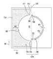
- チップ実装領域を有する基板;
前記チップ実装領域の周りの基板上に互いに隔たって配置される第1及び第2配線層;及び
前記チップ実装領域上に配置される複数の発光チップを含み、
前記第1配線層は、基準線の一側に配置され、第1湾曲部を有する第1配線パターン、及び前記第1配線パターンから前記基準線の他側に伸びる第1延長パターンを含み、
前記第2配線層は、前記基準線の他側に配置され、第2湾曲部を有する第2配線パターン、及び前記第2配線パターンから前記基準線の一側に伸びる第2延長パターンを含み、
前記基準線は前記チップ実装領域の中心を通る直線である、発光素子パッケージ。 - 前記第2湾曲部は前記第1湾曲部の反対方向に凹んでいる、請求項1に記載の発光素子パッケージ。
- 前記第1延長パターンは前記第1湾曲部の内周面の一端から伸び、前記第1延長パターンの末端は前記第1湾曲部の内周面の他端から離隔し、
前記第2延長パターンは前記第2湾曲部の内周面の一端から伸び、前記第2延長パターンの末端は前記第2湾曲部の内周面の他端から離隔する、請求項2に記載の発光素子パッケージ。 - 前記第1湾曲部及び前記第2湾曲部は半球形、楕円形又は多角形であり、前記第1延長パターン、及び前記第2延長パターンのそれぞれは曲線形状である、請求項1に記載の発光素子パッケージ。
- 前記第1延長パターンは、前記第1湾曲部の一端と連結される第1連結部、及び前記第1連結部と連結され、前記第1湾曲部の反対方向に凹んでいるライン形状の第1拡張部を含み、
前記第2延長パターンは、前記第2湾曲部の一端と連結される第2連結部、及び前記第2連結部と連結され、前記第2湾曲部の反対方向に凹んでいるライン形状の第2拡張部を含む、請求項1に記載の発光素子パッケージ。 - 前記第1連結部は前記第2湾曲部の他端と前記第2延長パターンの末端の間に配置され、
前記第2連結部は前記第1湾曲部の他端と前記第1延長パターンの末端の間に配置される、請求項5に記載の発光素子パッケージ。 - 前記第1連結部と前記第2連結部は前記基準線に平行な方向に向かい合う、請求項5に記載の発光素子パッケージ。
- 前記第1連結部と前記第1拡張部は互いに同一の幅を有し、前記第2連結部と前記第2拡張部は互いに同一の幅を有する、請求項5に記載の発光素子パッケージ。
- 前記第1湾曲部の他端と前記第1拡張部の末端の間には第1開口部が形成され、前記第2湾曲部の他端と前記第2拡張部の末端の間には第2開口部が形成され、
前記第1連結部は前記第2開口部を通過し、前記第2連結部は前記第1開口部を通過する、請求項5に記載の発光素子パッケージ。 - 前記第1開口部及び前記第2開口部は前記基準線に整列される、請求項9に記載の発光素子パッケージ。
- 前記第1配線層と前記第2配線層は前記チップ実装領域の中心を基準として原点対称である、請求項1に記載の発光素子パッケージ。
- 前記第1拡張部は前記第2湾曲部の内周面から一定距離で離隔するように前記第2湾曲部の内周面に沿って配置され、
前記第2拡張部は前記第1湾曲部の内周面から一定距離で離隔するように前記湾曲部の内周面に沿って配置される、請求項5に記載の発光素子パッケージ。 - 前記第1拡張部と前記第2湾曲部の内周面の間の離隔距離は前記第2拡張部と前記第1湾曲部の内周面の間の離隔距離と同一である、請求項12に記載の発光素子パッケージ。
- 前記基板は、
第1基板;及び
前記第1配線層と前記第2配線層を含み、前記チップ実装領域に対応する前記第1基板の一部を露出するように前記第1基板上に配置される第2基板を含む、請求項1に記載の発光素子パッケージ。 - 前記第1配線パターンと前記第1延長パターン上に配置される第1ボンディング層;及び
前記第2配線パターンと前記第2延長パターン上に配置される第2ボンディング層をさらに含む、請求項14に記載の発光素子パッケージ。 - 前記第1及び第2配線層上に配置され、前記第1及び第2ボンディング層を露出させる保護層をさらに含む、請求項15に記載の発光素子パッケージ。
- 前記第1ボンディング層と前記発光チップの少なくとも一つを連結する少なくとも一つの第1ワイヤ;及び
前記第2ボンディング層と前記発光チップの少なくとも一つを連結する少なくとも一つの第2ワイヤをさらに含む、請求項16に記載の発光素子パッケージ。 - 前記第1ボンディング層、及び前記第2ボンディング層上に配置され、前記第1及び第2ワイヤの一端を覆う隔壁部をさらに含む、請求項17に記載の発光素子パッケージ。
- 前記発光チップ、及び前記第1及び第2ワイヤを取り囲むように前記第2基板の溝部、及び前記隔壁部の内側を満たすモールディング部をさらに含む、請求項18に記載の発光素子パッケージ。
- 前記第1ボンディング層は前記第1湾曲部から既設定の距離以内に位置する前記第1配線パターンの上面の一領域、及び前記第1延長パターンの上面に配置され、前記第1湾曲部に隣り合い、
前記第2ボンディング層は前記第2湾曲部から既設定の距離以内に位置する前記第2配線パターンの上面の一領域、及び前記第2延長パターンの上面に配置され、前記第2湾曲部に隣り合う、請求項15に記載の発光素子パッケージ。 - 前記第1ボンディング層は、前記第1配線パターンと前記第1延長パターン上に配置され、互いに離隔し、前記第1湾曲部に隣り合う第1ボンディング部を含み、
前記第2ボンディング層は、前記第2配線パターンと前記第2延長パターン上に配置され、互いに離隔し、前記第2湾曲部に隣り合う第2ボンディング部を含む、請求項15に記載の発光素子パッケージ。 - チップ実装領域を有する基板;
基準線の一側の基板上に配置され、第1方向に凹んでいる第1湾曲部を有する第1配線パターン、及び前記第1湾曲部の一端と他端の間の内周面から第2方向に伸びる第1拡張部を有する第2延長パターンを含む第1配線層;
前記基準線の他側の基板上に配置され、前記第2方向に凹んでいる第2湾曲部を有する第2配線パターン、及び前記第2配線パターンの一端から前記基準線の一側に伸びる第2拡張部と前記第2配線パターンの他端から前記基準線の一側に伸びる第3拡張部を含む第2延長パターンを含む第2配線層;及び
前記チップ実装領域上に配置される複数の発光チップを含み、
前記第1延長パターンは前記第2拡張部の末端と前記第3拡張部の末端の間の空間を通過し、前記基準線は前記チップ実装領域の中心を通る直線であり、前記第1方向と前記第2方向は互いに反対方向である、発光素子パッケージ。 - 前記第1拡張部は前記チップ実装領域を取り囲む環形を有する、請求項22に記載の発光素子パッケージ。
- 前記第1拡張部上に配置される第1ボンディング層;及び
前記第2湾曲部から既設定の距離以内に位置する第2配線パターンの上面の一領域、及び前記第2延長パターン上に配置される第2ボンディング層をさらに含む、請求項23に記載の発光素子パッケージ。 - 前記第1延長パターン上に互いに隔たって配置される第1ボンディング部;及び
前記第2湾曲部から既設定の距離以内に位置する第2配線パターンの上面の一領域、及び前記第2延長パターン上に互いに隔たって配置される第2ボンディング部をさらに含む、請求項23に記載の発光素子パッケージ。 - 前記第1及び第2ボンディング層と前記前記発光チップを連結するワイヤ;及び
前記第1ボンディング層、及び前記第2ボンディング層上に配置され、前記第1及び第2ボンディング層と連結される前記ワイヤの一端を覆う隔壁部をさらに含む、請求項24に記載の発光素子パッケージ。 - 請求項1〜26のいずれか一項に記載の発光素子パッケージを含む光源モジュール;及び
前記光源モジュールの熱を発散させる放熱体を含む、照明装置。
Applications Claiming Priority (3)
| Application Number | Priority Date | Filing Date | Title |
|---|---|---|---|
| KR10-2014-0066271 | 2014-05-30 | ||
| KR1020140066271A KR102145919B1 (ko) | 2014-05-30 | 2014-05-30 | 발광 소자 패키지 |
| PCT/KR2015/004777 WO2015182899A1 (ko) | 2014-05-30 | 2015-05-13 | 발광 소자 패키지 |
Publications (3)
| Publication Number | Publication Date |
|---|---|
| JP2017517885A true JP2017517885A (ja) | 2017-06-29 |
| JP2017517885A5 JP2017517885A5 (ja) | 2018-06-07 |
| JP6578303B2 JP6578303B2 (ja) | 2019-09-18 |
Family
ID=54699182
Family Applications (1)
| Application Number | Title | Priority Date | Filing Date |
|---|---|---|---|
| JP2016567972A Active JP6578303B2 (ja) | 2014-05-30 | 2015-05-13 | 発光素子パッケージ |
Country Status (6)
| Country | Link |
|---|---|
| US (1) | US10396258B2 (ja) |
| EP (1) | EP3151291B1 (ja) |
| JP (1) | JP6578303B2 (ja) |
| KR (1) | KR102145919B1 (ja) |
| CN (1) | CN106463597B (ja) |
| WO (1) | WO2015182899A1 (ja) |
Families Citing this family (1)
| Publication number | Priority date | Publication date | Assignee | Title |
|---|---|---|---|---|
| JP7044412B1 (ja) | 2020-10-08 | 2022-03-30 | 丸茂電機株式会社 | Led光源装置およびled光源装置の製造方法 |
Citations (4)
| Publication number | Priority date | Publication date | Assignee | Title |
|---|---|---|---|---|
| JP2011028864A (ja) * | 2009-07-21 | 2011-02-10 | Citizen Electronics Co Ltd | 発光ダイオード光源装置 |
| JP2012230967A (ja) * | 2011-04-25 | 2012-11-22 | Mitsubishi Chemicals Corp | 配線基板、発光ダイオードモジュール |
| JP2014007342A (ja) * | 2012-06-26 | 2014-01-16 | Toshiba Lighting & Technology Corp | 発光モジュール及び照明装置 |
| JP2014067816A (ja) * | 2012-09-25 | 2014-04-17 | Toyoda Gosei Co Ltd | 発光装置 |
Family Cites Families (16)
| Publication number | Priority date | Publication date | Assignee | Title |
|---|---|---|---|---|
| JP2009289810A (ja) * | 2008-05-27 | 2009-12-10 | Toshiba Lighting & Technology Corp | 照明装置 |
| JP5263515B2 (ja) | 2008-10-20 | 2013-08-14 | 東芝ライテック株式会社 | 照明装置 |
| JP5428684B2 (ja) | 2009-09-11 | 2014-02-26 | 豊田合成株式会社 | 半導体発光素子 |
| JP5623062B2 (ja) * | 2009-11-13 | 2014-11-12 | シャープ株式会社 | 発光装置およびその製造方法 |
| JP5768435B2 (ja) * | 2010-04-16 | 2015-08-26 | 日亜化学工業株式会社 | 発光装置 |
| US9153561B2 (en) | 2010-04-16 | 2015-10-06 | Nichia Corporation | Light-emitting device comprising a metal film on a substrate and manufacturing method for the same |
| JP5481277B2 (ja) | 2010-06-04 | 2014-04-23 | シャープ株式会社 | 発光装置 |
| JP5537295B2 (ja) | 2010-07-05 | 2014-07-02 | パナソニック株式会社 | 発光素子実装用配線パターン、発光素子実装用配線パターンを有する発光素子実装用配線基板および発光素子実装用配線基板を用いた発光モジュールならびに発光モジュールを装備した照明器具 |
| BR112013001623B1 (pt) | 2010-07-23 | 2021-02-02 | Nichia Corporation | elemento emissor de luz |
| WO2012026695A2 (en) * | 2010-08-27 | 2012-03-01 | Seoul Opto Device Co., Ltd. | Light emitting diode with improved luminous efficiency |
| KR20120060306A (ko) * | 2010-12-02 | 2012-06-12 | 서울반도체 주식회사 | 발광 다이오드 모듈 및 발광 다이오드 조명장치 |
| JP5776203B2 (ja) | 2011-02-14 | 2015-09-09 | 日亜化学工業株式会社 | 発光素子 |
| KR101273819B1 (ko) | 2011-07-13 | 2013-06-11 | 한국수자원공사 | 사력댐 차수죤의 차수성 평가방법 |
| KR20140097284A (ko) * | 2011-11-07 | 2014-08-06 | 크리,인코포레이티드 | 고전압 어레이 발광다이오드(led) 장치, 기구 및 방법 |
| KR101911866B1 (ko) * | 2012-04-04 | 2018-10-25 | 엘지이노텍 주식회사 | 발광 소자 패키지 |
| JP6102677B2 (ja) | 2012-12-28 | 2017-03-29 | 日亜化学工業株式会社 | 発光素子 |
-
2014
- 2014-05-30 KR KR1020140066271A patent/KR102145919B1/ko active IP Right Grant
-
2015
- 2015-05-13 CN CN201580028735.8A patent/CN106463597B/zh active Active
- 2015-05-13 US US15/314,118 patent/US10396258B2/en active Active
- 2015-05-13 JP JP2016567972A patent/JP6578303B2/ja active Active
- 2015-05-13 WO PCT/KR2015/004777 patent/WO2015182899A1/ko active Application Filing
- 2015-05-13 EP EP15800384.8A patent/EP3151291B1/en active Active
Patent Citations (4)
| Publication number | Priority date | Publication date | Assignee | Title |
|---|---|---|---|---|
| JP2011028864A (ja) * | 2009-07-21 | 2011-02-10 | Citizen Electronics Co Ltd | 発光ダイオード光源装置 |
| JP2012230967A (ja) * | 2011-04-25 | 2012-11-22 | Mitsubishi Chemicals Corp | 配線基板、発光ダイオードモジュール |
| JP2014007342A (ja) * | 2012-06-26 | 2014-01-16 | Toshiba Lighting & Technology Corp | 発光モジュール及び照明装置 |
| JP2014067816A (ja) * | 2012-09-25 | 2014-04-17 | Toyoda Gosei Co Ltd | 発光装置 |
Also Published As
| Publication number | Publication date |
|---|---|
| US10396258B2 (en) | 2019-08-27 |
| CN106463597B (zh) | 2019-02-15 |
| EP3151291A1 (en) | 2017-04-05 |
| KR20150137784A (ko) | 2015-12-09 |
| EP3151291A4 (en) | 2017-04-26 |
| EP3151291B1 (en) | 2018-04-25 |
| CN106463597A (zh) | 2017-02-22 |
| US20170200874A1 (en) | 2017-07-13 |
| KR102145919B1 (ko) | 2020-08-19 |
| JP6578303B2 (ja) | 2019-09-18 |
| WO2015182899A1 (ko) | 2015-12-03 |
Similar Documents
| Publication | Publication Date | Title |
|---|---|---|
| EP2669946B1 (en) | Illumination device | |
| US8860072B2 (en) | Light emitting device and light unit having the same | |
| TWI527988B (zh) | 發光裝置及應用其之照明單元 | |
| JP5994472B2 (ja) | 発光装置 | |
| US8357948B2 (en) | Light emitting device and lighting system | |
| WO2013136389A1 (ja) | 基板、発光装置及び照明装置 | |
| JP2011254079A (ja) | 発光素子パッケージ及び照明システム | |
| JP6080053B2 (ja) | 発光モジュール | |
| JP6083253B2 (ja) | 発光装置の積層体 | |
| KR20160131527A (ko) | 자외선 발광 장치 | |
| US9822959B2 (en) | Light emitting device | |
| JP6578303B2 (ja) | 発光素子パッケージ | |
| KR101081170B1 (ko) | 발광 소자 패키지 및 그 제조방법 | |
| EP2325908A2 (en) | Light emitting device package | |
| JP6399057B2 (ja) | 発光装置 | |
| JP2018032748A (ja) | 発光装置、照明装置及び発光装置の製造方法 | |
| KR20130014755A (ko) | 발광 소자 패키지 및 조명 시스템 | |
| KR102142718B1 (ko) | 발광 소자 및 이를 구비한 조명 장치 | |
| TWM495626U (zh) | 具透光平板之發光裝置 | |
| JP5216948B1 (ja) | 基板、発光装置及び照明装置 | |
| KR20110110609A (ko) | 발광 소자 패키지 및 이를 구비한 라이트 유닛 | |
| JP2019021665A (ja) | 発光装置、照明装置、及び、実装基板 |
Legal Events
| Date | Code | Title | Description |
|---|---|---|---|
| A521 | Request for written amendment filed |
Free format text: JAPANESE INTERMEDIATE CODE: A523 Effective date: 20180420 |
|
| A621 | Written request for application examination |
Free format text: JAPANESE INTERMEDIATE CODE: A621 Effective date: 20180420 |
|
| A977 | Report on retrieval |
Free format text: JAPANESE INTERMEDIATE CODE: A971007 Effective date: 20190227 |
|
| A131 | Notification of reasons for refusal |
Free format text: JAPANESE INTERMEDIATE CODE: A131 Effective date: 20190312 |
|
| A521 | Request for written amendment filed |
Free format text: JAPANESE INTERMEDIATE CODE: A523 Effective date: 20190510 |
|
| TRDD | Decision of grant or rejection written | ||
| A01 | Written decision to grant a patent or to grant a registration (utility model) |
Free format text: JAPANESE INTERMEDIATE CODE: A01 Effective date: 20190820 |
|
| A61 | First payment of annual fees (during grant procedure) |
Free format text: JAPANESE INTERMEDIATE CODE: A61 Effective date: 20190826 |
|
| R150 | Certificate of patent or registration of utility model |
Ref document number: 6578303 Country of ref document: JP Free format text: JAPANESE INTERMEDIATE CODE: R150 |
|
| S531 | Written request for registration of change of domicile |
Free format text: JAPANESE INTERMEDIATE CODE: R313531 |
|
| S111 | Request for change of ownership or part of ownership |
Free format text: JAPANESE INTERMEDIATE CODE: R313113 |
|
| R350 | Written notification of registration of transfer |
Free format text: JAPANESE INTERMEDIATE CODE: R350 |
|
| R350 | Written notification of registration of transfer |
Free format text: JAPANESE INTERMEDIATE CODE: R350 |
|
| R250 | Receipt of annual fees |
Free format text: JAPANESE INTERMEDIATE CODE: R250 |
|
| R250 | Receipt of annual fees |
Free format text: JAPANESE INTERMEDIATE CODE: R250 |