EP2325908A2 - Light emitting device package - Google Patents
Light emitting device package Download PDFInfo
- Publication number
- EP2325908A2 EP2325908A2 EP20100192289 EP10192289A EP2325908A2 EP 2325908 A2 EP2325908 A2 EP 2325908A2 EP 20100192289 EP20100192289 EP 20100192289 EP 10192289 A EP10192289 A EP 10192289A EP 2325908 A2 EP2325908 A2 EP 2325908A2
- Authority
- EP
- European Patent Office
- Prior art keywords
- light emitting
- emitting device
- package
- thermal conductivity
- light
- Prior art date
- Legal status (The legal status is an assumption and is not a legal conclusion. Google has not performed a legal analysis and makes no representation as to the accuracy of the status listed.)
- Ceased
Links
Images


Classifications
-
- H—ELECTRICITY
- H01—ELECTRIC ELEMENTS
- H01L—SEMICONDUCTOR DEVICES NOT COVERED BY CLASS H10
- H01L33/00—Semiconductor devices with at least one potential-jump barrier or surface barrier specially adapted for light emission; Processes or apparatus specially adapted for the manufacture or treatment thereof or of parts thereof; Details thereof
- H01L33/48—Semiconductor devices with at least one potential-jump barrier or surface barrier specially adapted for light emission; Processes or apparatus specially adapted for the manufacture or treatment thereof or of parts thereof; Details thereof characterised by the semiconductor body packages
- H01L33/64—Heat extraction or cooling elements
- H01L33/641—Heat extraction or cooling elements characterized by the materials
-
- H—ELECTRICITY
- H01—ELECTRIC ELEMENTS
- H01L—SEMICONDUCTOR DEVICES NOT COVERED BY CLASS H10
- H01L33/00—Semiconductor devices with at least one potential-jump barrier or surface barrier specially adapted for light emission; Processes or apparatus specially adapted for the manufacture or treatment thereof or of parts thereof; Details thereof
- H01L33/48—Semiconductor devices with at least one potential-jump barrier or surface barrier specially adapted for light emission; Processes or apparatus specially adapted for the manufacture or treatment thereof or of parts thereof; Details thereof characterised by the semiconductor body packages
- H01L33/52—Encapsulations
- H01L33/56—Materials, e.g. epoxy or silicone resin
-
- H—ELECTRICITY
- H01—ELECTRIC ELEMENTS
- H01L—SEMICONDUCTOR DEVICES NOT COVERED BY CLASS H10
- H01L2224/00—Indexing scheme for arrangements for connecting or disconnecting semiconductor or solid-state bodies and methods related thereto as covered by H01L24/00
- H01L2224/01—Means for bonding being attached to, or being formed on, the surface to be connected, e.g. chip-to-package, die-attach, "first-level" interconnects; Manufacturing methods related thereto
- H01L2224/42—Wire connectors; Manufacturing methods related thereto
- H01L2224/47—Structure, shape, material or disposition of the wire connectors after the connecting process
- H01L2224/48—Structure, shape, material or disposition of the wire connectors after the connecting process of an individual wire connector
- H01L2224/4805—Shape
- H01L2224/4809—Loop shape
- H01L2224/48091—Arched
-
- H—ELECTRICITY
- H01—ELECTRIC ELEMENTS
- H01L—SEMICONDUCTOR DEVICES NOT COVERED BY CLASS H10
- H01L2224/00—Indexing scheme for arrangements for connecting or disconnecting semiconductor or solid-state bodies and methods related thereto as covered by H01L24/00
- H01L2224/01—Means for bonding being attached to, or being formed on, the surface to be connected, e.g. chip-to-package, die-attach, "first-level" interconnects; Manufacturing methods related thereto
- H01L2224/42—Wire connectors; Manufacturing methods related thereto
- H01L2224/47—Structure, shape, material or disposition of the wire connectors after the connecting process
- H01L2224/48—Structure, shape, material or disposition of the wire connectors after the connecting process of an individual wire connector
- H01L2224/481—Disposition
- H01L2224/48151—Connecting between a semiconductor or solid-state body and an item not being a semiconductor or solid-state body, e.g. chip-to-substrate, chip-to-passive
- H01L2224/48221—Connecting between a semiconductor or solid-state body and an item not being a semiconductor or solid-state body, e.g. chip-to-substrate, chip-to-passive the body and the item being stacked
- H01L2224/48245—Connecting between a semiconductor or solid-state body and an item not being a semiconductor or solid-state body, e.g. chip-to-substrate, chip-to-passive the body and the item being stacked the item being metallic
- H01L2224/48247—Connecting between a semiconductor or solid-state body and an item not being a semiconductor or solid-state body, e.g. chip-to-substrate, chip-to-passive the body and the item being stacked the item being metallic connecting the wire to a bond pad of the item
-
- H—ELECTRICITY
- H01—ELECTRIC ELEMENTS
- H01L—SEMICONDUCTOR DEVICES NOT COVERED BY CLASS H10
- H01L2924/00—Indexing scheme for arrangements or methods for connecting or disconnecting semiconductor or solid-state bodies as covered by H01L24/00
- H01L2924/30—Technical effects
- H01L2924/301—Electrical effects
- H01L2924/3011—Impedance
Definitions
- the present invention relates to a light emitting device package.
- a light emitting diode is a semiconductor light emitting device that converts current into light.
- a wavelength of light emitted from the LED may vary depending on a semiconductor material used for manufacturing the LED. This is because the wavelength of the emitted light varies depending on the energy difference between valance band electrons and conduction band electrons, that is, the bandgap of the semiconductor material.
- the LED generates light having high brightness, so that the LED has been extensively used as a light source for a display device, a vehicle, or a lighting device.
- the LED can represent a white color having superior light efficiency by employing luminescence materials or combining LEDs having various colors.
- the LED package is used for packaging LED chip structure which includes several semiconductor layers.
- the LED package provides electrical power to the LED chip and activates it.
- the LED package is capable of protecting the vulnerable LED chip from outside circumstances, and enhancing the efficiency of lighting.
- LED chip Since LED chip generates a high amount of heat, it is also important to consider the factor for heat dissipation when designing an LED package. If the heat is not dissipated properly, the reliability of LED chip may decrease.
- the LED package of the prior art most of the heat generated is dissipated to the electrode which is placed under the LED package body. Namely, almost of the heat is transferred to merely one direction. Therefore, the technical problem of the prior art is that it does not dissipate the heat efficiently.
- the present invention provides a light emitting device package capable of improving a heat dissipation characteristic of heat energy.
- a light emitting device package includes a package body, a light emitting device in a cavity of the package body, an encapsulation layer for covering the light emitting device, and an electrode connected to the light emitting device.
- the encapsulation layer may comprise a resin layer.
- the package body may include a material having thermal conductivity lower than that of a material constituting the encapsulation layer. The difference of the thermal conductivity between the package body and the encapsulation layer cause the heat generated by the LED device to flow through the encapsulation layer, which improve the efficiency of heat dissipation.
- the difference in thermal conductivity between materials of the package body and the encapsulation layer can be at least 10W/m.K.
- the electrode may have thermal conductivity higher than that of the encapsulation layer.
- the electrode may be attached to a lower portion of the light emitting device.
- the electrode may include alloy of copper or aluminum.
- the light emitting device package further comprises a lens part placed on the encapsulation layer.
- the package body may include a material having thermal conductivity lower than thermal conductivity of a material constituting the lens part.
- the encapsulation layer may include at least one kind of phosphor. The difference in thermal conductivity between materials constituting the package body and the lens part may be at least 0.01W/m.K.
- the encapsulation layer may transfer heat emitted from the light emitting device to the lens part and the electrode.
- the heat is dissipated in part to the electrode under the LED package body and in part to other directions, through the encapsulation layer, rather than to the package body.
- the cavity of the light emitting device package may include a first cavity filled with the encapsulation layer, and a second cavity filled with the lens part.
- the first and second cavities may have a step difference.
- a lighting system comprising a light emitting module including a substrate and a light emitting device package according to the embodiment is also provided.
- the dissipation path of heat energy emitted from the light emitting diode can be provided. Accordingly, the heat dissipation characteristic can be improved.
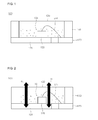
- FIG. 1 is a side sectional view showing a light emitting device package according to the present invention
- FIG. 2 is a view showing a heat dissipation characteristic of the light emitting device package of FIG. 1
- FIG. 3 is a view showing a simulation result obtained in the comparison with a conventional light emitting device package in order to explain the heat dissipation effect of the light emitting device package according to the first embodiment;
- a light emitting device package 100 includes first and second electrodes 121 and 123 formed on a substrate, a light emitting device 125 mounted on the first electrode 121, and a package body 110 surrounding the light emitting device 125 at an upper portion of the substrate.
- An encapsulation layer 130 is provided in a cavity of the package body 110 to seal the light emitting device 125, and a phosphor 131 is contained in the encapsulation layer 130.
- the cavity forms a predetermined space in the package body 110, and the light emitting device 125 and the encapsulation layer 130 are placed in the cavity.
- the first and second electrodes 121 and 123 are configured to connect to anode and cathode terminals of the light emitting device 125, respectively.
- the first and second electrodes 121 and 123 may be formed through a printing scheme.
- the first and second electrodes 121 and 123 are electrically insulated from each other, and pass through the package body 110.
- the first and second electrodes 121 and 123 can reflect light emitted from the light emitting device 125 to increase light efficiency. According to the embodiment, the first and second electrodes 121 and 123 dissipate heat emitted from the light emitting device 125.
- the first and second electrodes 121 and 123 include metallic material including copper or aluminum representing superior electrical conductivity.
- the light emitting device 125 may include a lateral type light emitting device in which both of an N side electrode layer and a P side electrode layer are provided on a top surface of a light emitting device structure, a flip-chip type light emitting device in which both of the N side electrode layer and the P side electrode layer are provided on a bottom surface of the light emitting device structure, or a vertical type light emitting device in which the N side electrode layer and the P side electrode layer are provided on the top and bottom surfaces of the light emitting device structure, respectively.
- FIG. 1 shows a vertical type light emitting device
- an N side electrode layer of the light emitting device 125 is electrically connected to the first electrode 121 through a wire 127, and a P side electrode layer of the light emitting device 125 makes contact with the second electrode 123.
- the light emitting device 125 may include a light emitting diode including an N type semiconductor layer, an active layer, and a P type semiconductor layer.
- the package body 110 including the cavity is formed on the first and second electrodes 121 and 123 while surrounding the light emitting device 125. If the internal surface of the package body 110, that is, the inner peripheral surface forming the cavity has a predetermined inclination, the reflection of light emitted from the light emitting device 125 is increased, so that light emission efficiency can be improved.
- the package body 110 includes a material having low thermal conductivity, and materials of the package body 110 are selected based on materials constituting the encapsulation layer 130.
- Heat emitted according to the driving of the light emitting device 125 is dissipated by using the difference in thermal conductivity between materials of the package body 110 and the encapsulation layer 130.
- the package body 110 may constitute a material having thermal conductivity that is at least 10W/m.K less than the thermal conductivity of a material of the encapsulation layer 130.
- the package body 110 may have thermal conductivity that is 0.01W/m.K less than the thermal conductivity of a material constituting the encapsulation layer 130.
- heat generated from the light emitting device 125 may be transferred to the first and second electrodes 121 and 123 having high thermal conductivity and emitted in the upward direction, rather than transferred to the package body 110 having low thermal conductivity.
- heat transferred to the encapsulation layer 130 is transferred to the first and second electrodes 121 and 123 having thermal conductivity higher than that of the encapsulation layer 130, so that heat dissipation property can be improved.
- a heat transfer path is formed by using the difference in thermal conductivity between the materials of the package body 110 and the encapsulation layer 130, and the heat dissipation characteristic can be improved through the heat transfer path.
- the heat transfer path is marked as "H" of FIG. 2 , and emitted heat under the encapsulation layer 130 is transferred in the upward direction of the light emitting device 125 and transferred to the first and second electrodes 121 and 123 under the light emitting device 125, rather than transferred to the package body 110 having lower thermal conductivity.
- FIGS. 3A and 3B An experimental result for the above structure is shown in FIGS. 3A and 3B.
- FIG. 3A shows a simulation result of a conventional light emitting device package in which an encapsulation layer includes silicon and a package body includes synthetic resin so that the encapsulation layer and the package body have thermal conductivity similar to each other.
- FIG. 3B shows a simulation result of the light emitting device package according to the present embodiment including the encapsulation layer 130 including a material having thermal conductivity that is at least 10W/m.K greater than the thermal conductivity of a material constituting the package body 110.
- the peak temperature is represented as about 93.4°C, and the thermal resistance is represented as about 68.4[K/W].
- the peak temperature is represented as about 74°C, and the thermal resistance is represented as about 49[K/W].
- the thermal transfer path may be recognized.
- an excessively small amount of heat is dissipated to the outside through an upper portion of the encapsulation layer, and the heat dissipation is concentrated on a metallic electrode.
- the package body 110 which includes a material having thermal conductivity at least 10W/m.K less than the thermal conductivity of the encapsulation layer 130, represents a superior heat dissipation characteristic.
- FIG. 4 is a side sectional view showing a light emitting device package of the present invention.
- structures and components previously described will be not further described.
- the light emitting device package 100 includes a first cavity 115, a second cavity 117, a first electrode 121, a second electrode 123, a package body 110, a light emitting device 125, a resin member 140, and a lens part 150.
- First ends of the first and second electrodes 121 and 123 may be provided in the first cavity 115 of the package body 110, and an inner peripheral wall of the first cavity 115 may be perpendicular or inclined with respect to a bottom surface of the fist cavity 115.
- the light emitting device 125 may be provided in the first cavity 115, and may be provided on at least one electrode 121.
- the first electrode 121 may be electrically connected to the second electrode 123.
- a plurality of LED chips may be installed in the first cavity 115. In this case, the patterns of the first and second electrodes 121 and 123 may be changed.
- the package body 110 may be provided therein with the second cavity 117, and the second cavity 117 is formed at an upper portion of the package body 110.
- the first cavity 115 is provided at a central lower portion of the second cavity 117.
- a diameter of the second cavity 117 may be greater than that of an upper portion of the first cavity 115.
- the space of the first cavity 115 and/or the second cavity 117 may be defined by the package body 110 and/or at least one electrode 121 and 123, and the space may have various shapes.
- the resin member 140 is formed in the first cavity 115.
- the resin member 140 may include at least one phosphor and/or a diffusing agent, but the embodiment is not limited thereto.
- the phosphor may include a yellow, green, red, or blue phosphor.
- the surface of the resin member 140 may have a concave shape, a convex shape, or a flat shape. A predetermined pattern may be formed on the surface of the resin member 140.
- the first cavity 115 and the second cavity 117 in the package body 110 may have the shape of a circular recess or a polygonal recess when viewed in a plan view.
- a part of light emitted from the light emitting device 125 may be reflected by a circumferential surface of the first cavity 115 or may be transmitted through the circumferential surface of the first cavity 115.
- the package body 110 according to the second embodiment may include a material having low thermal conductivity.
- the package body 110 may include a material having thermal conductivity at least 10W/m.K less than the thermal conductivity of a material constituting the lens part 150.
- the package body 110 may have thermal conductivity 0.01 times larger than thermal conductivity of the material constituting the lens part 150.
- the thermal conductivity of the lens part 150 may be identical to or higher than that of the resin member 140.
- the package body 110 may include a material having thermal conductivity that is at least 10W/m.K less than the thermal conductivity of a material constituting a member (for example, the lens part) provided in the cavity such that the heat dissipation path can be formed.
- the dissipation of the package body is achieved through the metallic electrodes 121 and 123 and the lens part 150, so that the heat dissipation path is formed in up and down directions of the light emitting device 125.
- the dissipation characteristic of heat emitted according to the driving of the light emitting device can be improved.
- the light emitting device package according to the embodiment may serve as a lighting system such as a backlight unit, an indicator, a lamp or a streetlamp.
- FIG. 5 is a perspective view showing a backlight unit 1100 including the light emitting device package according to the disclosure.
- the backlight unit 1100 shown in FIG. 5 is an example of a lighting system and the embodiment is not limited thereto.
- the backlight unit 1100 includes a bottom cover 1140, a light guide member 1120 installed in the bottom cover 1140, and a light emitting module 1110 installed at one side or over the bottom surface of the light guide member 1120.
- a reflective sheet 1130 is disposed under the light guide member 1120.
- the bottom cover 1140 has a box shape having an open top surface to receive the light guide member 1120, the light emitting module 1110 and the reflective sheet 1130 therein.
- the bottom cover 1140 may include metallic material or resin material, but the embodiment is not limited thereto.
- the light emitting module 1110 may include a plurality of light emitting devices 600 installed over a substrate 700.
- the light emitting devices 600 provide the light to the light guide member 1120.
- the light emitting module 1110 is installed over at least one inner side of the bottom cover 1140 to provide the light to at least one side of the light guide member 1120.
- the light emitting module 1110 can be provided under the light guide member 1120 in the bottom cover 1140 to provide the light toward the bottom surface of the light guide member 1120. Such an arrangement can be variously changed according to the design of the backlight unit 1100.
- the light guide member 1120 is installed in the bottom cover 1140.
- the light guide member 1120 converts the light emitted from the light emitting module 1110 into the surface light to guide the surface light toward a display panel (not shown).
- the light guide member 1120 may include a light guide plate.
- the light guide plate may include one of acryl-based resin, such as PMMA (polymethyl methacrylate), PET (polyethylene terephthalate), COC, PC (polycarbonate) or PEN (polyethylene naphthalate) resin.
- An optical sheet 1150 may be provided over the light guide member 1120.
- the optical sheet 1150 may include at least one of a diffusion sheet, a light collection sheet, a brightness enhancement sheet, and a fluorescent sheet.
- the optical sheet 1150 has a stack structure of the diffusion sheet, the light collection sheet, the brightness enhancement sheet, and the fluorescent sheet.
- the diffusion sheet uniformly diffuses the light emitted from the light emitting module 1110 such that the diffused light can be collected over the display panel (not shown) by the light collection sheet.
- the light output from the light collection sheet is randomly polarized and the brightness enhancement sheet increases the degree of polarization of the light output from the light collection sheet.
- the light collection sheet may include a horizontal and/or vertical prism sheet.
- the brightness enhancement sheet may include a dual brightness enhancement film and the fluorescent sheet may include a transmissive plate or a transmissive film including phosphors.
- the reflective sheet 1130 can be disposed under the light guide member 1120.
- the reflective sheet 1130 reflects the light, which is emitted through the bottom surface of the light guide member 1120, toward the light exit surface of the light guide member 1120.
- the reflective sheet 1130 may include resin material having a high reflectance, such as PET, PC or PVC resin, but the embodiment is not limited thereto.
- FIG. 6 is a perspective view showing a lighting system 1200 including the light emitting device according to the disclosure.
- the lighting system 1200 shown in FIG. 6 is only one example and the embodiment is not limited thereto.
- the lighting system 1200 includes a case body 1210, a light emitting module 1230 installed in the case body 1210, and a connection terminal 1220 installed in the case body 1210 to receive power from an external power source.
- the case body 1210 includes material having superior heat dissipation property.
- the case body 1210 includes metallic material or resin material.
- the light emitting module 1230 may include a substrate 700 and at least one light emitting device 600 installed over the substrate 700.
- the substrate 700 includes an insulating member printed with a circuit pattern.
- the substrate 700 includes a PCB (printed circuit board), an MC (metal core) PCB, an F (flexible) PCB, or a ceramic PCB.
- the substrate 700 may include material that effectively reflects the light.
- the surface of the substrate 700 can be coated with a color, such as a white color or a silver color, to effectively reflect the light.
- At least one light emitting device 600 can be installed over the substrate 700.
- Each light emitting device 600 may include at least one LED (light emitting diode).
- the LED may include a colored LED that emits the light having the color of red, green, blue or white and a UV (ultraviolet) LED that emits UV light.
- the light emitting module 1230 can be variously arranged to provide various colors and brightness.
- the white LED, the red LED and the green LED can be arranged to achieve the high color rendering index (CRI).
- a fluorescent sheet can be provided in the path of the light emitted from the light emitting module 1230 to change the wavelength of the light emitted from the light emitting module 1230.
- the fluorescent sheet may include yellow phosphors. In this case, the light emitted from the light emitting module 1230 passes through the fluorescent sheet so that the light is viewed as white light.
- connection terminal 1220 is electrically connected to the light emitting module 1230 to supply power to the light emitting module 1230.
- the connection terminal 1220 has a shape of a socket screw-coupled with the external power source, but the embodiment is not limited thereto.
- the connection terminal 1220 can be prepared in the form of a pin inserted into the external power source or connected to the external power source through a wire.
- At least one of the light guide member, the diffusion sheet, the light collection sheet, the brightness enhancement sheet and the fluorescent sheet is provided in the path of the light emitted from the light emitting module, so that the desired optical effect can be achieved.
- the backlight unit 1100 and the lighting system 1200 of FIGS. 5 and 6 include the light emitting modules 1110 and 1230 including the light emitting device package of FIGS.1 to 4 , so that superior light efficiency can be acquired.
- any reference in this specification to "one embodiment,” “an embodiment,” “example embodiment,” etc. means that a particular feature, structure, or characteristic described in connection with the embodiment is included in at least one embodiment of the invention.
- the appearances of such phrases in various places in the specification are not necessarily all referring to the same embodiment.
Abstract
Description
- The present invention relates to a light emitting device package.
- A light emitting diode (LED) is a semiconductor light emitting device that converts current into light.
- A wavelength of light emitted from the LED may vary depending on a semiconductor material used for manufacturing the LED. This is because the wavelength of the emitted light varies depending on the energy difference between valance band electrons and conduction band electrons, that is, the bandgap of the semiconductor material.
- The LED generates light having high brightness, so that the LED has been extensively used as a light source for a display device, a vehicle, or a lighting device. In addition, the LED can represent a white color having superior light efficiency by employing luminescence materials or combining LEDs having various colors.
- The LED package is used for packaging LED chip structure which includes several semiconductor layers. The LED package provides electrical power to the LED chip and activates it. Moreover, the LED package is capable of protecting the vulnerable LED chip from outside circumstances, and enhancing the efficiency of lighting.
- Electrical energy applied to a light emitting diode is mainly converted into optical energy and heat energy. Since LED chip generates a high amount of heat, it is also important to consider the factor for heat dissipation when designing an LED package. If the heat is not dissipated properly, the reliability of LED chip may decrease.
- According to the LED package of the prior art, most of the heat generated is dissipated to the electrode which is placed under the LED package body. Namely, almost of the heat is transferred to merely one direction. Therefore, the technical problem of the prior art is that it does not dissipate the heat efficiently.
- The present invention provides a light emitting device package capable of improving a heat dissipation characteristic of heat energy.
- According to the present invention, a light emitting device package includes a package body, a light emitting device in a cavity of the package body, an encapsulation layer for covering the light emitting device, and an electrode connected to the light emitting device. The encapsulation layer may comprise a resin layer. The package body may include a material having thermal conductivity lower than that of a material constituting the encapsulation layer. The difference of the thermal conductivity between the package body and the encapsulation layer cause the heat generated by the LED device to flow through the encapsulation layer, which improve the efficiency of heat dissipation. The difference in thermal conductivity between materials of the package body and the encapsulation layer can be at least 10W/m.K.
- According to another aspect of the embodiment, the electrode may have thermal conductivity higher than that of the encapsulation layer. The electrode may be attached to a lower portion of the light emitting device. The electrode may include alloy of copper or aluminum.
- According to another aspect of the embodiment, the light emitting device package further comprises a lens part placed on the encapsulation layer. The package body may include a material having thermal conductivity lower than thermal conductivity of a material constituting the lens part. The encapsulation layer may include at least one kind of phosphor. The difference in thermal conductivity between materials constituting the package body and the lens part may be at least 0.01W/m.K. The encapsulation layer may transfer heat emitted from the light emitting device to the lens part and the electrode.
- Thus, according to the invention, the heat is dissipated in part to the electrode under the LED package body and in part to other directions, through the encapsulation layer, rather than to the package body.
- According to another aspect of the embodiment, the cavity of the light emitting device package may include a first cavity filled with the encapsulation layer, and a second cavity filled with the lens part. The first and second cavities may have a step difference.
- A lighting system comprising a light emitting module including a substrate and a light emitting device package according to the embodiment is also provided.
- According to the light emitting device package, the dissipation path of heat energy emitted from the light emitting diode can be provided. Accordingly, the heat dissipation characteristic can be improved.
-
-
FIG. 1 is a side sectional view showing a light emitting device package according to the present invention; -
FIG. 2 is a view showing the heat dissipation characteristic of the light emitting device package ofFIG. 1 ; -
FIGS. 3A and 3B are views showing a simulation result obtained in the comparison with a conventional light emitting device package in order to explain the heat dissipation effect of the light emitting device package according to the first embodiment; -
FIG. 4 is a side sectional view showing a light emitting device package of the present invention; -
FIG. 5 is a perspective view showing a backlight unit including a light emitting device package according to the present invention; and -
FIG. 6 is a view showing a lighting system including a light emitting device according to the present invention. - In the description of the embodiments, it will be understood that, when a layer (or film), a region, a pattern, or a structure is referred to as being "on" or "under" another substrate, another layer (or film), another region, another pad, or another pattern, it can be "directly" or "indirectly" over the other substrate, layer (or film), region, pad, or pattern, or one or more intervening layers may also be present. Such a position of the layer has been described with reference to the drawings.
- The drawing figures which show cross-sections through a semiconductor wafer or device are not drawn to scale but rather to highlight major features of the invention. The thickness and size of each layer shown in the drawings may be exaggerated, omitted or schematically drawn for the purpose of convenience or clarity. In addition, the size of elements does not utterly reflect an actual size. The process steps and the structures described herein below do not form a complete process flow for manufacturing integrated circuits. In fact, this invention can be practiced jointly with integrated circuit manufacturing techniques currently used in the art, and only those common process steps will be discussed herein as are necessary to an understanding of the invention.
- Hereinafter, a light emitting device package according to embodiments will be described in detail with reference to accompanying drawings.
-
FIG. 1 is a side sectional view showing a light emitting device package according to the present invention,FIG. 2 is a view showing a heat dissipation characteristic of the light emitting device package ofFIG. 1 , andFIG. 3 is a view showing a simulation result obtained in the comparison with a conventional light emitting device package in order to explain the heat dissipation effect of the light emitting device package according to the first embodiment; - Referring to
FIG. 1 , a lightemitting device package 100 includes first andsecond electrodes light emitting device 125 mounted on thefirst electrode 121, and apackage body 110 surrounding thelight emitting device 125 at an upper portion of the substrate. - An
encapsulation layer 130 is provided in a cavity of thepackage body 110 to seal thelight emitting device 125, and aphosphor 131 is contained in theencapsulation layer 130. In other words, the cavity forms a predetermined space in thepackage body 110, and thelight emitting device 125 and theencapsulation layer 130 are placed in the cavity. - The first and
second electrodes light emitting device 125, respectively. The first andsecond electrodes second electrodes package body 110. - The first and
second electrodes light emitting device 125 to increase light efficiency. According to the embodiment, the first andsecond electrodes light emitting device 125. The first andsecond electrodes - The
light emitting device 125 may include a lateral type light emitting device in which both of an N side electrode layer and a P side electrode layer are provided on a top surface of a light emitting device structure, a flip-chip type light emitting device in which both of the N side electrode layer and the P side electrode layer are provided on a bottom surface of the light emitting device structure, or a vertical type light emitting device in which the N side electrode layer and the P side electrode layer are provided on the top and bottom surfaces of the light emitting device structure, respectively. - Although
FIG. 1 shows a vertical type light emitting device, an N side electrode layer of thelight emitting device 125 is electrically connected to thefirst electrode 121 through awire 127, and a P side electrode layer of thelight emitting device 125 makes contact with thesecond electrode 123. For example, thelight emitting device 125 may include a light emitting diode including an N type semiconductor layer, an active layer, and a P type semiconductor layer. - The
package body 110 including the cavity is formed on the first andsecond electrodes light emitting device 125. If the internal surface of thepackage body 110, that is, the inner peripheral surface forming the cavity has a predetermined inclination, the reflection of light emitted from thelight emitting device 125 is increased, so that light emission efficiency can be improved. In particular, thepackage body 110 includes a material having low thermal conductivity, and materials of thepackage body 110 are selected based on materials constituting theencapsulation layer 130. - Heat emitted according to the driving of the
light emitting device 125 is dissipated by using the difference in thermal conductivity between materials of thepackage body 110 and theencapsulation layer 130. For example, thepackage body 110 may constitute a material having thermal conductivity that is at least 10W/m.K less than the thermal conductivity of a material of theencapsulation layer 130. - Preferably, the
package body 110 may have thermal conductivity that is 0.01W/m.K less than the thermal conductivity of a material constituting theencapsulation layer 130. - Therefore, heat generated from the
light emitting device 125 may be transferred to the first andsecond electrodes package body 110 having low thermal conductivity. - In other words, heat transferred to the
encapsulation layer 130 is transferred to the first andsecond electrodes encapsulation layer 130, so that heat dissipation property can be improved. - Therefore, a heat transfer path is formed by using the difference in thermal conductivity between the materials of the
package body 110 and theencapsulation layer 130, and the heat dissipation characteristic can be improved through the heat transfer path. - In the light emitting device package according to the present embodiment, the heat transfer path is marked as "H" of
FIG. 2 , and emitted heat under theencapsulation layer 130 is transferred in the upward direction of thelight emitting device 125 and transferred to the first andsecond electrodes light emitting device 125, rather than transferred to thepackage body 110 having lower thermal conductivity. - An experimental result for the above structure is shown in
FIGS. 3A and 3B. FIG. 3A shows a simulation result of a conventional light emitting device package in which an encapsulation layer includes silicon and a package body includes synthetic resin so that the encapsulation layer and the package body have thermal conductivity similar to each other.FIG. 3B shows a simulation result of the light emitting device package according to the present embodiment including theencapsulation layer 130 including a material having thermal conductivity that is at least 10W/m.K greater than the thermal conductivity of a material constituting thepackage body 110. - According to the experimental result, in the case of the conventional light emitting device package, the peak temperature is represented as about 93.4°C, and the thermal resistance is represented as about 68.4[K/W]. In contrast, in the case of the light emitting device package according to the present embodiment, the peak temperature is represented as about 74°C, and the thermal resistance is represented as about 49[K/W].
- As shown in
FIGS. 3A and 3B , the thermal transfer path may be recognized. In the case of the conventional light emitting device package, an excessively small amount of heat is dissipated to the outside through an upper portion of the encapsulation layer, and the heat dissipation is concentrated on a metallic electrode. - In contrast, in the case of the light emitting device package according to the present embodiment, heat dissipation simultaneously occurs toward the metallic electrode and toward the outside through the upper portion of the
encapsulation layer 130. In other words, when comparing with thepackage body 110 including only metal, thepackage body 110, which includes a material having thermal conductivity at least 10W/m.K less than the thermal conductivity of theencapsulation layer 130, represents a superior heat dissipation characteristic. -
FIG. 4 is a side sectional view showing a light emitting device package of the present invention. In the following description, structures and components previously described will be not further described. - Referring to
FIG. 4 , the light emittingdevice package 100 includes afirst cavity 115, asecond cavity 117, afirst electrode 121, asecond electrode 123, apackage body 110, alight emitting device 125, aresin member 140, and alens part 150. - First ends of the first and
second electrodes first cavity 115 of thepackage body 110, and an inner peripheral wall of thefirst cavity 115 may be perpendicular or inclined with respect to a bottom surface of thefist cavity 115. Thelight emitting device 125 may be provided in thefirst cavity 115, and may be provided on at least oneelectrode 121. Thefirst electrode 121 may be electrically connected to thesecond electrode 123. In addition, a plurality of LED chips may be installed in thefirst cavity 115. In this case, the patterns of the first andsecond electrodes - The
package body 110 may be provided therein with thesecond cavity 117, and thesecond cavity 117 is formed at an upper portion of thepackage body 110. Thefirst cavity 115 is provided at a central lower portion of thesecond cavity 117. A diameter of thesecond cavity 117 may be greater than that of an upper portion of thefirst cavity 115. - The space of the
first cavity 115 and/or thesecond cavity 117 may be defined by thepackage body 110 and/or at least oneelectrode - The
resin member 140 is formed in thefirst cavity 115. Theresin member 140 may include at least one phosphor and/or a diffusing agent, but the embodiment is not limited thereto. The phosphor may include a yellow, green, red, or blue phosphor. In addition, the surface of theresin member 140 may have a concave shape, a convex shape, or a flat shape. A predetermined pattern may be formed on the surface of theresin member 140. - The
first cavity 115 and thesecond cavity 117 in thepackage body 110 may have the shape of a circular recess or a polygonal recess when viewed in a plan view. A part of light emitted from thelight emitting device 125 may be reflected by a circumferential surface of thefirst cavity 115 or may be transmitted through the circumferential surface of thefirst cavity 115. - The
package body 110 according to the second embodiment may include a material having low thermal conductivity. In other words, thepackage body 110 may include a material having thermal conductivity at least 10W/m.K less than the thermal conductivity of a material constituting thelens part 150. Preferably, thepackage body 110 may have thermal conductivity 0.01 times larger than thermal conductivity of the material constituting thelens part 150. - The thermal conductivity of the
lens part 150 may be identical to or higher than that of theresin member 140. - Heat emitted from the
light emitting device 125 is transferred to the first andsecond electrodes lens part 150 having higher thermal conductivity, rather than transferred to thepackage body 110 having lower thermal conductivity, so that the heat can be dissipated. In other words, similarly to the first embodiment, thepackage body 110 may include a material having thermal conductivity that is at least 10W/m.K less than the thermal conductivity of a material constituting a member (for example, the lens part) provided in the cavity such that the heat dissipation path can be formed. - Therefore, the dissipation of the package body is achieved through the
metallic electrodes lens part 150, so that the heat dissipation path is formed in up and down directions of thelight emitting device 125. - As described above, according to the present embodiment, the dissipation characteristic of heat emitted according to the driving of the light emitting device can be improved.
- The light emitting device package according to the embodiment may serve as a lighting system such as a backlight unit, an indicator, a lamp or a streetlamp.
- Hereinafter, applications of the disclosure will be described with reference to
FIGS. 5 and6 . -
FIG. 5 is a perspective view showing abacklight unit 1100 including the light emitting device package according to the disclosure. - The
backlight unit 1100 shown inFIG. 5 is an example of a lighting system and the embodiment is not limited thereto. - Referring to
FIG. 5 , thebacklight unit 1100 includes abottom cover 1140, alight guide member 1120 installed in thebottom cover 1140, and alight emitting module 1110 installed at one side or over the bottom surface of thelight guide member 1120. In addition, areflective sheet 1130 is disposed under thelight guide member 1120. - The
bottom cover 1140 has a box shape having an open top surface to receive thelight guide member 1120, thelight emitting module 1110 and thereflective sheet 1130 therein. In addition, thebottom cover 1140 may include metallic material or resin material, but the embodiment is not limited thereto. - The
light emitting module 1110 may include a plurality of light emittingdevices 600 installed over asubstrate 700. Thelight emitting devices 600 provide the light to thelight guide member 1120. - As shown in
FIG. 5 , thelight emitting module 1110 is installed over at least one inner side of thebottom cover 1140 to provide the light to at least one side of thelight guide member 1120. - In addition, the
light emitting module 1110 can be provided under thelight guide member 1120 in thebottom cover 1140 to provide the light toward the bottom surface of thelight guide member 1120. Such an arrangement can be variously changed according to the design of thebacklight unit 1100. - The
light guide member 1120 is installed in thebottom cover 1140. Thelight guide member 1120 converts the light emitted from thelight emitting module 1110 into the surface light to guide the surface light toward a display panel (not shown). - The
light guide member 1120 may include a light guide plate. For instance, the light guide plate may include one of acryl-based resin, such as PMMA (polymethyl methacrylate), PET (polyethylene terephthalate), COC, PC (polycarbonate) or PEN (polyethylene naphthalate) resin. - An
optical sheet 1150 may be provided over thelight guide member 1120. - The
optical sheet 1150 may include at least one of a diffusion sheet, a light collection sheet, a brightness enhancement sheet, and a fluorescent sheet. For instance, theoptical sheet 1150 has a stack structure of the diffusion sheet, the light collection sheet, the brightness enhancement sheet, and the fluorescent sheet. In this case, the diffusion sheet uniformly diffuses the light emitted from thelight emitting module 1110 such that the diffused light can be collected over the display panel (not shown) by the light collection sheet. The light output from the light collection sheet is randomly polarized and the brightness enhancement sheet increases the degree of polarization of the light output from the light collection sheet. The light collection sheet may include a horizontal and/or vertical prism sheet. In addition, the brightness enhancement sheet may include a dual brightness enhancement film and the fluorescent sheet may include a transmissive plate or a transmissive film including phosphors. - The
reflective sheet 1130 can be disposed under thelight guide member 1120. Thereflective sheet 1130 reflects the light, which is emitted through the bottom surface of thelight guide member 1120, toward the light exit surface of thelight guide member 1120. Thereflective sheet 1130 may include resin material having a high reflectance, such as PET, PC or PVC resin, but the embodiment is not limited thereto. -
FIG. 6 is a perspective view showing alighting system 1200 including the light emitting device according to the disclosure. Thelighting system 1200 shown inFIG. 6 is only one example and the embodiment is not limited thereto. - Referring to
FIG. 6 , thelighting system 1200 includes acase body 1210, alight emitting module 1230 installed in thecase body 1210, and aconnection terminal 1220 installed in thecase body 1210 to receive power from an external power source. - Preferably, the
case body 1210 includes material having superior heat dissipation property. For instance, thecase body 1210 includes metallic material or resin material. - The
light emitting module 1230 may include asubstrate 700 and at least one light emittingdevice 600 installed over thesubstrate 700. - The
substrate 700 includes an insulating member printed with a circuit pattern. For instance, thesubstrate 700 includes a PCB (printed circuit board), an MC (metal core) PCB, an F (flexible) PCB, or a ceramic PCB. - In addition, the
substrate 700 may include material that effectively reflects the light. The surface of thesubstrate 700 can be coated with a color, such as a white color or a silver color, to effectively reflect the light. - At least one light emitting
device 600 can be installed over thesubstrate 700. - Each
light emitting device 600 may include at least one LED (light emitting diode). The LED may include a colored LED that emits the light having the color of red, green, blue or white and a UV (ultraviolet) LED that emits UV light. - The
light emitting module 1230 can be variously arranged to provide various colors and brightness. For instance, the white LED, the red LED and the green LED can be arranged to achieve the high color rendering index (CRI). In addition, a fluorescent sheet can be provided in the path of the light emitted from thelight emitting module 1230 to change the wavelength of the light emitted from thelight emitting module 1230. For instance, if the light emitted from thelight emitting module 1230 has a wavelength band of blue light, the fluorescent sheet may include yellow phosphors. In this case, the light emitted from thelight emitting module 1230 passes through the fluorescent sheet so that the light is viewed as white light. - The
connection terminal 1220 is electrically connected to thelight emitting module 1230 to supply power to thelight emitting module 1230. Referring toFIG. 6 , theconnection terminal 1220 has a shape of a socket screw-coupled with the external power source, but the embodiment is not limited thereto. For instance, theconnection terminal 1220 can be prepared in the form of a pin inserted into the external power source or connected to the external power source through a wire. - According to the lighting system as described above, at least one of the light guide member, the diffusion sheet, the light collection sheet, the brightness enhancement sheet and the fluorescent sheet is provided in the path of the light emitted from the light emitting module, so that the desired optical effect can be achieved.
- The
backlight unit 1100 and thelighting system 1200 ofFIGS. 5 and6 include thelight emitting modules FIGS.1 to 4 , so that superior light efficiency can be acquired. - Any reference in this specification to "one embodiment," "an embodiment," "example embodiment," etc., means that a particular feature, structure, or characteristic described in connection with the embodiment is included in at least one embodiment of the invention. The appearances of such phrases in various places in the specification are not necessarily all referring to the same embodiment. Further, when a particular feature, structure, or characteristic is described in connection with any embodiment, it is submitted that it is within the purview of one skilled in the art to effect such feature, structure, or characteristic in connection with other ones of the embodiments.
- Although embodiments have been described with reference to a number of illustrative embodiments thereof, it should be understood that numerous other modifications and embodiments can be devised by those skilled in the art that will fall within the spirit and scope of the principles of this disclosure. More particularly, various variations and modifications are possible in the component parts and/or arrangements of the subject combination arrangement within the scope of the disclosure, the drawings and the appended claims. In addition to variations and modifications in the component parts and/or arrangements, alternative uses will also be apparent to those skilled in the art.
Claims (13)
- A light emitting device package comprising:a package body (110);a light emitting device (125) in a cavity of the package body (110);a resin layer (130) for covering the light emitting device (125); andan electrode (121, 123) connected to the light emitting device (125),characterized in that the package body (110) includes a material having thermal conductivity lower than thermal conductivity of a material constituting the resin layer (130),anda difference in thermal conductivity between materials of the package body (110) and the resin layer (130) is at least 10W/m.K.
- The light emitting device package of claim 1, wherein the resin layer (130) is placed in the cavity of the package body (110).
- The light emitting device package of claim 1, wherein the electrode (121, 123) has thermal conductivity higher than thermal conductivity of the resin layer (130).
- The light emitting device package of claim 1, wherein the electrode (121, 123) is attached to a lower portion of the light emitting device (125).
- The light emitting device package of claim 1, wherein the electrode (121, 123) includes alloy of copper or aluminum.
- The light emitting device package of claim 1, further comprising a lens part (117) placed on the resin layer (130).
- The light emitting device package of claim 6, wherein the package body (110) includes a material having thermal conductivity lower than thermal conductivity of a material of the lens part (150).
- The light emitting device package of claim 6, wherein the resin layer (130) includes at least one kind of phosphor.
- The light emitting device package of claim 6, wherein the cavity includes:a first cavity (115) filled with the resin layer (130); anda second cavity (117) filled with the lens part (150).
- The light emitting device package of claim 9, wherein the first and second cavities (115, 117) have a step difference.
- The light emitting device package of claim 6, wherein a difference in thermal conductivity between materials constituting the package body (110) and the lens part (117) is at least 0.01W/m.K.
- The light emitting device package of claim 6, wherein the resin layer transfers heat emitted from the light emitting device (125) to the lens part (150) and the electrode (121, 123).
- A lighting system comprising a light emitting module including a substrate and a light emitting device package claimed in one of claim 1 to 12 and provided on the substrate.
Applications Claiming Priority (1)
| Application Number | Priority Date | Filing Date | Title |
|---|---|---|---|
| KR1020090113141A KR101163850B1 (en) | 2009-11-23 | 2009-11-23 | Light emitting device package |
Publications (2)
| Publication Number | Publication Date |
|---|---|
| EP2325908A2 true EP2325908A2 (en) | 2011-05-25 |
| EP2325908A3 EP2325908A3 (en) | 2014-09-10 |
Family
ID=43480695
Family Applications (1)
| Application Number | Title | Priority Date | Filing Date |
|---|---|---|---|
| EP20100192289 Ceased EP2325908A3 (en) | 2009-11-23 | 2010-11-23 | Light emitting device package |
Country Status (5)
| Country | Link |
|---|---|
| US (1) | US8791482B2 (en) |
| EP (1) | EP2325908A3 (en) |
| JP (1) | JP2011114342A (en) |
| KR (1) | KR101163850B1 (en) |
| CN (1) | CN102082223B (en) |
Families Citing this family (3)
| Publication number | Priority date | Publication date | Assignee | Title |
|---|---|---|---|---|
| KR20140121507A (en) * | 2013-04-05 | 2014-10-16 | 크루셜텍 (주) | LED module for flash and method for fabricating the sme |
| KR101523664B1 (en) * | 2013-06-11 | 2015-05-29 | 주식회사 세미콘라이트 | Manufacturing method of metal substrate and semiconductor light emitting device comprising the metal substrate manufactured by the same |
| US9640709B2 (en) * | 2013-09-10 | 2017-05-02 | Heptagon Micro Optics Pte. Ltd. | Compact opto-electronic modules and fabrication methods for such modules |
Family Cites Families (21)
| Publication number | Priority date | Publication date | Assignee | Title |
|---|---|---|---|---|
| JPH1051034A (en) | 1996-08-01 | 1998-02-20 | Rohm Co Ltd | Surface-mount electronic component, its manufacture, method for mounting the component on circuit board, and circuit board mounting the component |
| US6867542B1 (en) * | 2000-03-29 | 2005-03-15 | General Electric Company | Floating chip photonic device and method of manufacture |
| JP3891115B2 (en) * | 2001-04-17 | 2007-03-14 | 日亜化学工業株式会社 | Light emitting device |
| GB0203588D0 (en) * | 2002-02-14 | 2002-04-03 | Enfis Ltd | A light system |
| US7244965B2 (en) * | 2002-09-04 | 2007-07-17 | Cree Inc, | Power surface mount light emitting die package |
| US7264378B2 (en) * | 2002-09-04 | 2007-09-04 | Cree, Inc. | Power surface mount light emitting die package |
| JP4192619B2 (en) | 2003-02-17 | 2008-12-10 | 豊田合成株式会社 | Light emitting diode lamp device |
| US6835960B2 (en) * | 2003-03-03 | 2004-12-28 | Opto Tech Corporation | Light emitting diode package structure |
| TW595017B (en) * | 2003-04-17 | 2004-06-21 | Arima Optoelectronics Corp | Light-emitting diode with high thermal conductivity and its manufacturing method |
| JP4645071B2 (en) * | 2003-06-20 | 2011-03-09 | 日亜化学工業株式会社 | Package molded body and semiconductor device using the same |
| JP2005252219A (en) * | 2004-02-06 | 2005-09-15 | Toyoda Gosei Co Ltd | Light emitting device and sealing member |
| JP2006206721A (en) * | 2005-01-27 | 2006-08-10 | Kansai Electric Power Co Inc:The | Highly heat-resistant synthetic polymer compound and semiconductor device of high dielectric strength coated with the same |
| JPWO2007018039A1 (en) * | 2005-08-05 | 2009-02-19 | パナソニック株式会社 | Semiconductor light emitting device |
| JP2008270709A (en) * | 2006-10-31 | 2008-11-06 | Techno Polymer Co Ltd | Heat-dissipating resin composition, substrate for mounting led, reflector, and substrate for mounting led provided with reflector portion |
| JP5233170B2 (en) * | 2007-05-31 | 2013-07-10 | 日亜化学工業株式会社 | LIGHT EMITTING DEVICE, RESIN MOLDED BODY FORMING LIGHT EMITTING DEVICE, AND METHOD FOR PRODUCING THEM |
| KR101360732B1 (en) * | 2007-06-27 | 2014-02-07 | 엘지이노텍 주식회사 | Led package |
| US8748922B2 (en) | 2007-09-04 | 2014-06-10 | Koninklijke Philips N.V. | Light output device |
| JP2009071090A (en) * | 2007-09-14 | 2009-04-02 | Toshiba Lighting & Technology Corp | Light-emitting device |
| US8337029B2 (en) * | 2008-01-17 | 2012-12-25 | Intematix Corporation | Light emitting device with phosphor wavelength conversion |
| KR101274816B1 (en) | 2008-02-14 | 2013-06-13 | 주식회사 엘지화학 | Resin composition having high heat resistance, thermal conductivity and reflectivity and the method of the same |
| JP2011023460A (en) | 2009-07-14 | 2011-02-03 | Panasonic Corp | Method of manufacturing light emitting device and light emitting device |
-
2009
- 2009-11-23 KR KR1020090113141A patent/KR101163850B1/en active IP Right Grant
-
2010
- 2010-11-17 JP JP2010256650A patent/JP2011114342A/en active Pending
- 2010-11-18 US US12/949,414 patent/US8791482B2/en active Active
- 2010-11-23 EP EP20100192289 patent/EP2325908A3/en not_active Ceased
- 2010-11-23 CN CN201010559362.6A patent/CN102082223B/en active Active
Non-Patent Citations (1)
| Title |
|---|
| None |
Also Published As
| Publication number | Publication date |
|---|---|
| EP2325908A3 (en) | 2014-09-10 |
| CN102082223A (en) | 2011-06-01 |
| JP2011114342A (en) | 2011-06-09 |
| KR20110056704A (en) | 2011-05-31 |
| CN102082223B (en) | 2015-07-15 |
| US8791482B2 (en) | 2014-07-29 |
| US20110121340A1 (en) | 2011-05-26 |
| KR101163850B1 (en) | 2012-07-09 |
Similar Documents
| Publication | Publication Date | Title |
|---|---|---|
| US8519427B2 (en) | Light emitting device and lighting system | |
| KR102024291B1 (en) | Lamp unit and vehicle lamp apparatus for using the same | |
| US8357948B2 (en) | Light emitting device and lighting system | |
| EP2337072A2 (en) | Light emitting device and light unit using the same | |
| US9293672B2 (en) | Light emitting device package | |
| EP2355194A2 (en) | Light emitting device package | |
| US8598616B2 (en) | Light emitting device and light unit using the same | |
| US20110175119A1 (en) | Light emitting apparatus and lighting system | |
| US9048395B2 (en) | Light emitting device package, lighting module and lighting system | |
| KR101655463B1 (en) | Light emitting device package and light unit having the same | |
| KR101734539B1 (en) | Light emitting device, method for fabricating the light emitting device, lighting unit comprising the light emitting device, and lighting device | |
| EP2813758B1 (en) | Light emitting module | |
| KR20140004351A (en) | Light emitting diode package | |
| US8791482B2 (en) | Light emitting device package | |
| KR101655464B1 (en) | Light emitting device package, method for fabricating the same and lighting system including the same | |
| KR20150017594A (en) | Lighting apparatus | |
| KR101924014B1 (en) | Light emitting device package and lighting system having the same | |
| KR20110125067A (en) | Light-emitting element package | |
| KR20110108097A (en) | Light emitting device package and lighting system including the same | |
| KR101655462B1 (en) | Light emitting device and lighting device using the same | |
| KR102229467B1 (en) | Lighting device | |
| KR102229476B1 (en) | Lighting device | |
| KR101637590B1 (en) | Light emitting device package and lighting system | |
| KR20120000975A (en) | Light emitting device package, method for manufacturing the same, and lighting system | |
| KR20130094973A (en) | Lighting device |
Legal Events
| Date | Code | Title | Description |
|---|---|---|---|
| PUAI | Public reference made under article 153(3) epc to a published international application that has entered the european phase |
Free format text: ORIGINAL CODE: 0009012 |
|
| 17P | Request for examination filed |
Effective date: 20101123 |
|
| AK | Designated contracting states |
Kind code of ref document: A2 Designated state(s): AL AT BE BG CH CY CZ DE DK EE ES FI FR GB GR HR HU IE IS IT LI LT LU LV MC MK MT NL NO PL PT RO RS SE SI SK SM TR |
|
| AX | Request for extension of the european patent |
Extension state: BA ME |
|
| RBV | Designated contracting states (corrected) |
Designated state(s): AL AT BE BG CH CY CZ DE DK EE ES FI FR GB GR HR HU IE IS IT LI LT LU LV MC MK MT NL NO PL PT RO RS SE SI SK SM TR |
|
| PUAL | Search report despatched |
Free format text: ORIGINAL CODE: 0009013 |
|
| AK | Designated contracting states |
Kind code of ref document: A3 Designated state(s): AL AT BE BG CH CY CZ DE DK EE ES FI FR GB GR HR HU IE IS IT LI LT LU LV MC MK MT NL NO PL PT RO RS SE SI SK SM TR |
|
| AX | Request for extension of the european patent |
Extension state: BA ME |
|
| RIC1 | Information provided on ipc code assigned before grant |
Ipc: H01L 33/64 20100101ALN20140801BHEP Ipc: H01L 33/56 20100101AFI20140801BHEP |
|
| 17Q | First examination report despatched |
Effective date: 20150506 |
|
| STAA | Information on the status of an ep patent application or granted ep patent |
Free format text: STATUS: THE APPLICATION HAS BEEN REFUSED |
|
| 18R | Application refused |
Effective date: 20160510 |