JP2017183665A - Substrate carrier device, substrate processing apparatus, and substrate processing method - Google Patents
Substrate carrier device, substrate processing apparatus, and substrate processing method Download PDFInfo
- Publication number
- JP2017183665A JP2017183665A JP2016073092A JP2016073092A JP2017183665A JP 2017183665 A JP2017183665 A JP 2017183665A JP 2016073092 A JP2016073092 A JP 2016073092A JP 2016073092 A JP2016073092 A JP 2016073092A JP 2017183665 A JP2017183665 A JP 2017183665A
- Authority
- JP
- Japan
- Prior art keywords
- substrate
- processing
- unit
- claw
- plate
- Prior art date
- Legal status (The legal status is an assumption and is not a legal conclusion. Google has not performed a legal analysis and makes no representation as to the accuracy of the status listed.)
- Pending
Links
- 239000000758 substrate Substances 0.000 title claims abstract description 351
- 238000012545 processing Methods 0.000 title claims abstract description 164
- 238000003672 processing method Methods 0.000 title claims abstract description 6
- 238000012546 transfer Methods 0.000 claims abstract description 90
- 230000002093 peripheral effect Effects 0.000 claims abstract description 15
- 210000000078 claw Anatomy 0.000 claims description 87
- 230000003028 elevating effect Effects 0.000 claims description 23
- 238000003860 storage Methods 0.000 claims description 17
- 239000007788 liquid Substances 0.000 description 36
- 230000007246 mechanism Effects 0.000 description 15
- 230000032258 transport Effects 0.000 description 15
- 238000000034 method Methods 0.000 description 11
- 230000008569 process Effects 0.000 description 10
- 239000000356 contaminant Substances 0.000 description 4
- 238000004140 cleaning Methods 0.000 description 3
- 238000003780 insertion Methods 0.000 description 3
- 230000037431 insertion Effects 0.000 description 3
- 238000004904 shortening Methods 0.000 description 3
- 230000005484 gravity Effects 0.000 description 2
- 239000004973 liquid crystal related substance Substances 0.000 description 2
- 239000002245 particle Substances 0.000 description 2
- 238000013459 approach Methods 0.000 description 1
- FFBHFFJDDLITSX-UHFFFAOYSA-N benzyl N-[2-hydroxy-4-(3-oxomorpholin-4-yl)phenyl]carbamate Chemical compound OC1=C(NC(=O)OCC2=CC=CC=C2)C=CC(=C1)N1CCOCC1=O FFBHFFJDDLITSX-UHFFFAOYSA-N 0.000 description 1
- 230000008602 contraction Effects 0.000 description 1
- 230000000694 effects Effects 0.000 description 1
- 238000004519 manufacturing process Methods 0.000 description 1
- 238000012986 modification Methods 0.000 description 1
- 230000004048 modification Effects 0.000 description 1
- 230000004044 response Effects 0.000 description 1
- 239000004065 semiconductor Substances 0.000 description 1
Images


Classifications
-
- B—PERFORMING OPERATIONS; TRANSPORTING
- B60—VEHICLES IN GENERAL
- B60K—ARRANGEMENT OR MOUNTING OF PROPULSION UNITS OR OF TRANSMISSIONS IN VEHICLES; ARRANGEMENT OR MOUNTING OF PLURAL DIVERSE PRIME-MOVERS IN VEHICLES; AUXILIARY DRIVES FOR VEHICLES; INSTRUMENTATION OR DASHBOARDS FOR VEHICLES; ARRANGEMENTS IN CONNECTION WITH COOLING, AIR INTAKE, GAS EXHAUST OR FUEL SUPPLY OF PROPULSION UNITS IN VEHICLES
- B60K35/00—Instruments specially adapted for vehicles; Arrangement of instruments in or on vehicles
- B60K35/20—Output arrangements, i.e. from vehicle to user, associated with vehicle functions or specially adapted therefor
- B60K35/28—Output arrangements, i.e. from vehicle to user, associated with vehicle functions or specially adapted therefor characterised by the type of the output information, e.g. video entertainment or vehicle dynamics information; characterised by the purpose of the output information, e.g. for attracting the attention of the driver
-
- B—PERFORMING OPERATIONS; TRANSPORTING
- B60—VEHICLES IN GENERAL
- B60K—ARRANGEMENT OR MOUNTING OF PROPULSION UNITS OR OF TRANSMISSIONS IN VEHICLES; ARRANGEMENT OR MOUNTING OF PLURAL DIVERSE PRIME-MOVERS IN VEHICLES; AUXILIARY DRIVES FOR VEHICLES; INSTRUMENTATION OR DASHBOARDS FOR VEHICLES; ARRANGEMENTS IN CONNECTION WITH COOLING, AIR INTAKE, GAS EXHAUST OR FUEL SUPPLY OF PROPULSION UNITS IN VEHICLES
- B60K35/00—Instruments specially adapted for vehicles; Arrangement of instruments in or on vehicles
- B60K35/20—Output arrangements, i.e. from vehicle to user, associated with vehicle functions or specially adapted therefor
- B60K35/29—Instruments characterised by the way in which information is handled, e.g. showing information on plural displays or prioritising information according to driving conditions
-
- H—ELECTRICITY
- H01—ELECTRIC ELEMENTS
- H01L—SEMICONDUCTOR DEVICES NOT COVERED BY CLASS H10
- H01L21/00—Processes or apparatus adapted for the manufacture or treatment of semiconductor or solid state devices or of parts thereof
- H01L21/67—Apparatus specially adapted for handling semiconductor or electric solid state devices during manufacture or treatment thereof; Apparatus specially adapted for handling wafers during manufacture or treatment of semiconductor or electric solid state devices or components ; Apparatus not specifically provided for elsewhere
- H01L21/67005—Apparatus not specifically provided for elsewhere
- H01L21/67011—Apparatus for manufacture or treatment
- H01L21/67155—Apparatus for manufacturing or treating in a plurality of work-stations
- H01L21/67161—Apparatus for manufacturing or treating in a plurality of work-stations characterized by the layout of the process chambers
- H01L21/67173—Apparatus for manufacturing or treating in a plurality of work-stations characterized by the layout of the process chambers in-line arrangement
-
- H—ELECTRICITY
- H01—ELECTRIC ELEMENTS
- H01L—SEMICONDUCTOR DEVICES NOT COVERED BY CLASS H10
- H01L21/00—Processes or apparatus adapted for the manufacture or treatment of semiconductor or solid state devices or of parts thereof
- H01L21/67—Apparatus specially adapted for handling semiconductor or electric solid state devices during manufacture or treatment thereof; Apparatus specially adapted for handling wafers during manufacture or treatment of semiconductor or electric solid state devices or components ; Apparatus not specifically provided for elsewhere
- H01L21/67005—Apparatus not specifically provided for elsewhere
- H01L21/67011—Apparatus for manufacture or treatment
- H01L21/67155—Apparatus for manufacturing or treating in a plurality of work-stations
- H01L21/67184—Apparatus for manufacturing or treating in a plurality of work-stations characterized by the presence of more than one transfer chamber
-
- H—ELECTRICITY
- H01—ELECTRIC ELEMENTS
- H01L—SEMICONDUCTOR DEVICES NOT COVERED BY CLASS H10
- H01L21/00—Processes or apparatus adapted for the manufacture or treatment of semiconductor or solid state devices or of parts thereof
- H01L21/67—Apparatus specially adapted for handling semiconductor or electric solid state devices during manufacture or treatment thereof; Apparatus specially adapted for handling wafers during manufacture or treatment of semiconductor or electric solid state devices or components ; Apparatus not specifically provided for elsewhere
- H01L21/677—Apparatus specially adapted for handling semiconductor or electric solid state devices during manufacture or treatment thereof; Apparatus specially adapted for handling wafers during manufacture or treatment of semiconductor or electric solid state devices or components ; Apparatus not specifically provided for elsewhere for conveying, e.g. between different workstations
- H01L21/67739—Apparatus specially adapted for handling semiconductor or electric solid state devices during manufacture or treatment thereof; Apparatus specially adapted for handling wafers during manufacture or treatment of semiconductor or electric solid state devices or components ; Apparatus not specifically provided for elsewhere for conveying, e.g. between different workstations into and out of processing chamber
- H01L21/67742—Mechanical parts of transfer devices
-
- H—ELECTRICITY
- H01—ELECTRIC ELEMENTS
- H01L—SEMICONDUCTOR DEVICES NOT COVERED BY CLASS H10
- H01L21/00—Processes or apparatus adapted for the manufacture or treatment of semiconductor or solid state devices or of parts thereof
- H01L21/67—Apparatus specially adapted for handling semiconductor or electric solid state devices during manufacture or treatment thereof; Apparatus specially adapted for handling wafers during manufacture or treatment of semiconductor or electric solid state devices or components ; Apparatus not specifically provided for elsewhere
- H01L21/677—Apparatus specially adapted for handling semiconductor or electric solid state devices during manufacture or treatment thereof; Apparatus specially adapted for handling wafers during manufacture or treatment of semiconductor or electric solid state devices or components ; Apparatus not specifically provided for elsewhere for conveying, e.g. between different workstations
- H01L21/67739—Apparatus specially adapted for handling semiconductor or electric solid state devices during manufacture or treatment thereof; Apparatus specially adapted for handling wafers during manufacture or treatment of semiconductor or electric solid state devices or components ; Apparatus not specifically provided for elsewhere for conveying, e.g. between different workstations into and out of processing chamber
- H01L21/67748—Apparatus specially adapted for handling semiconductor or electric solid state devices during manufacture or treatment thereof; Apparatus specially adapted for handling wafers during manufacture or treatment of semiconductor or electric solid state devices or components ; Apparatus not specifically provided for elsewhere for conveying, e.g. between different workstations into and out of processing chamber horizontal transfer of a single workpiece
-
- H—ELECTRICITY
- H01—ELECTRIC ELEMENTS
- H01L—SEMICONDUCTOR DEVICES NOT COVERED BY CLASS H10
- H01L21/00—Processes or apparatus adapted for the manufacture or treatment of semiconductor or solid state devices or of parts thereof
- H01L21/67—Apparatus specially adapted for handling semiconductor or electric solid state devices during manufacture or treatment thereof; Apparatus specially adapted for handling wafers during manufacture or treatment of semiconductor or electric solid state devices or components ; Apparatus not specifically provided for elsewhere
- H01L21/677—Apparatus specially adapted for handling semiconductor or electric solid state devices during manufacture or treatment thereof; Apparatus specially adapted for handling wafers during manufacture or treatment of semiconductor or electric solid state devices or components ; Apparatus not specifically provided for elsewhere for conveying, e.g. between different workstations
- H01L21/67739—Apparatus specially adapted for handling semiconductor or electric solid state devices during manufacture or treatment thereof; Apparatus specially adapted for handling wafers during manufacture or treatment of semiconductor or electric solid state devices or components ; Apparatus not specifically provided for elsewhere for conveying, e.g. between different workstations into and out of processing chamber
- H01L21/67751—Apparatus specially adapted for handling semiconductor or electric solid state devices during manufacture or treatment thereof; Apparatus specially adapted for handling wafers during manufacture or treatment of semiconductor or electric solid state devices or components ; Apparatus not specifically provided for elsewhere for conveying, e.g. between different workstations into and out of processing chamber vertical transfer of a single workpiece
-
- H—ELECTRICITY
- H01—ELECTRIC ELEMENTS
- H01L—SEMICONDUCTOR DEVICES NOT COVERED BY CLASS H10
- H01L21/00—Processes or apparatus adapted for the manufacture or treatment of semiconductor or solid state devices or of parts thereof
- H01L21/67—Apparatus specially adapted for handling semiconductor or electric solid state devices during manufacture or treatment thereof; Apparatus specially adapted for handling wafers during manufacture or treatment of semiconductor or electric solid state devices or components ; Apparatus not specifically provided for elsewhere
- H01L21/677—Apparatus specially adapted for handling semiconductor or electric solid state devices during manufacture or treatment thereof; Apparatus specially adapted for handling wafers during manufacture or treatment of semiconductor or electric solid state devices or components ; Apparatus not specifically provided for elsewhere for conveying, e.g. between different workstations
- H01L21/67739—Apparatus specially adapted for handling semiconductor or electric solid state devices during manufacture or treatment thereof; Apparatus specially adapted for handling wafers during manufacture or treatment of semiconductor or electric solid state devices or components ; Apparatus not specifically provided for elsewhere for conveying, e.g. between different workstations into and out of processing chamber
- H01L21/67757—Apparatus specially adapted for handling semiconductor or electric solid state devices during manufacture or treatment thereof; Apparatus specially adapted for handling wafers during manufacture or treatment of semiconductor or electric solid state devices or components ; Apparatus not specifically provided for elsewhere for conveying, e.g. between different workstations into and out of processing chamber vertical transfer of a batch of workpieces
-
- H—ELECTRICITY
- H01—ELECTRIC ELEMENTS
- H01L—SEMICONDUCTOR DEVICES NOT COVERED BY CLASS H10
- H01L21/00—Processes or apparatus adapted for the manufacture or treatment of semiconductor or solid state devices or of parts thereof
- H01L21/67—Apparatus specially adapted for handling semiconductor or electric solid state devices during manufacture or treatment thereof; Apparatus specially adapted for handling wafers during manufacture or treatment of semiconductor or electric solid state devices or components ; Apparatus not specifically provided for elsewhere
- H01L21/677—Apparatus specially adapted for handling semiconductor or electric solid state devices during manufacture or treatment thereof; Apparatus specially adapted for handling wafers during manufacture or treatment of semiconductor or electric solid state devices or components ; Apparatus not specifically provided for elsewhere for conveying, e.g. between different workstations
- H01L21/67763—Apparatus specially adapted for handling semiconductor or electric solid state devices during manufacture or treatment thereof; Apparatus specially adapted for handling wafers during manufacture or treatment of semiconductor or electric solid state devices or components ; Apparatus not specifically provided for elsewhere for conveying, e.g. between different workstations the wafers being stored in a carrier, involving loading and unloading
- H01L21/67766—Mechanical parts of transfer devices
-
- H—ELECTRICITY
- H01—ELECTRIC ELEMENTS
- H01L—SEMICONDUCTOR DEVICES NOT COVERED BY CLASS H10
- H01L21/00—Processes or apparatus adapted for the manufacture or treatment of semiconductor or solid state devices or of parts thereof
- H01L21/67—Apparatus specially adapted for handling semiconductor or electric solid state devices during manufacture or treatment thereof; Apparatus specially adapted for handling wafers during manufacture or treatment of semiconductor or electric solid state devices or components ; Apparatus not specifically provided for elsewhere
- H01L21/677—Apparatus specially adapted for handling semiconductor or electric solid state devices during manufacture or treatment thereof; Apparatus specially adapted for handling wafers during manufacture or treatment of semiconductor or electric solid state devices or components ; Apparatus not specifically provided for elsewhere for conveying, e.g. between different workstations
- H01L21/67763—Apparatus specially adapted for handling semiconductor or electric solid state devices during manufacture or treatment thereof; Apparatus specially adapted for handling wafers during manufacture or treatment of semiconductor or electric solid state devices or components ; Apparatus not specifically provided for elsewhere for conveying, e.g. between different workstations the wafers being stored in a carrier, involving loading and unloading
- H01L21/67769—Storage means
-
- H—ELECTRICITY
- H01—ELECTRIC ELEMENTS
- H01L—SEMICONDUCTOR DEVICES NOT COVERED BY CLASS H10
- H01L21/00—Processes or apparatus adapted for the manufacture or treatment of semiconductor or solid state devices or of parts thereof
- H01L21/67—Apparatus specially adapted for handling semiconductor or electric solid state devices during manufacture or treatment thereof; Apparatus specially adapted for handling wafers during manufacture or treatment of semiconductor or electric solid state devices or components ; Apparatus not specifically provided for elsewhere
- H01L21/677—Apparatus specially adapted for handling semiconductor or electric solid state devices during manufacture or treatment thereof; Apparatus specially adapted for handling wafers during manufacture or treatment of semiconductor or electric solid state devices or components ; Apparatus not specifically provided for elsewhere for conveying, e.g. between different workstations
- H01L21/67763—Apparatus specially adapted for handling semiconductor or electric solid state devices during manufacture or treatment thereof; Apparatus specially adapted for handling wafers during manufacture or treatment of semiconductor or electric solid state devices or components ; Apparatus not specifically provided for elsewhere for conveying, e.g. between different workstations the wafers being stored in a carrier, involving loading and unloading
- H01L21/67778—Apparatus specially adapted for handling semiconductor or electric solid state devices during manufacture or treatment thereof; Apparatus specially adapted for handling wafers during manufacture or treatment of semiconductor or electric solid state devices or components ; Apparatus not specifically provided for elsewhere for conveying, e.g. between different workstations the wafers being stored in a carrier, involving loading and unloading involving loading and unloading of wafers
- H01L21/67781—Batch transfer of wafers
-
- H—ELECTRICITY
- H01—ELECTRIC ELEMENTS
- H01L—SEMICONDUCTOR DEVICES NOT COVERED BY CLASS H10
- H01L21/00—Processes or apparatus adapted for the manufacture or treatment of semiconductor or solid state devices or of parts thereof
- H01L21/67—Apparatus specially adapted for handling semiconductor or electric solid state devices during manufacture or treatment thereof; Apparatus specially adapted for handling wafers during manufacture or treatment of semiconductor or electric solid state devices or components ; Apparatus not specifically provided for elsewhere
- H01L21/683—Apparatus specially adapted for handling semiconductor or electric solid state devices during manufacture or treatment thereof; Apparatus specially adapted for handling wafers during manufacture or treatment of semiconductor or electric solid state devices or components ; Apparatus not specifically provided for elsewhere for supporting or gripping
- H01L21/687—Apparatus specially adapted for handling semiconductor or electric solid state devices during manufacture or treatment thereof; Apparatus specially adapted for handling wafers during manufacture or treatment of semiconductor or electric solid state devices or components ; Apparatus not specifically provided for elsewhere for supporting or gripping using mechanical means, e.g. chucks, clamps or pinches
- H01L21/68707—Apparatus specially adapted for handling semiconductor or electric solid state devices during manufacture or treatment thereof; Apparatus specially adapted for handling wafers during manufacture or treatment of semiconductor or electric solid state devices or components ; Apparatus not specifically provided for elsewhere for supporting or gripping using mechanical means, e.g. chucks, clamps or pinches the wafers being placed on a robot blade, or gripped by a gripper for conveyance
-
- H—ELECTRICITY
- H01—ELECTRIC ELEMENTS
- H01L—SEMICONDUCTOR DEVICES NOT COVERED BY CLASS H10
- H01L21/00—Processes or apparatus adapted for the manufacture or treatment of semiconductor or solid state devices or of parts thereof
- H01L21/67—Apparatus specially adapted for handling semiconductor or electric solid state devices during manufacture or treatment thereof; Apparatus specially adapted for handling wafers during manufacture or treatment of semiconductor or electric solid state devices or components ; Apparatus not specifically provided for elsewhere
- H01L21/683—Apparatus specially adapted for handling semiconductor or electric solid state devices during manufacture or treatment thereof; Apparatus specially adapted for handling wafers during manufacture or treatment of semiconductor or electric solid state devices or components ; Apparatus not specifically provided for elsewhere for supporting or gripping
- H01L21/687—Apparatus specially adapted for handling semiconductor or electric solid state devices during manufacture or treatment thereof; Apparatus specially adapted for handling wafers during manufacture or treatment of semiconductor or electric solid state devices or components ; Apparatus not specifically provided for elsewhere for supporting or gripping using mechanical means, e.g. chucks, clamps or pinches
- H01L21/68714—Apparatus specially adapted for handling semiconductor or electric solid state devices during manufacture or treatment thereof; Apparatus specially adapted for handling wafers during manufacture or treatment of semiconductor or electric solid state devices or components ; Apparatus not specifically provided for elsewhere for supporting or gripping using mechanical means, e.g. chucks, clamps or pinches the wafers being placed on a susceptor, stage or support
- H01L21/68742—Apparatus specially adapted for handling semiconductor or electric solid state devices during manufacture or treatment thereof; Apparatus specially adapted for handling wafers during manufacture or treatment of semiconductor or electric solid state devices or components ; Apparatus not specifically provided for elsewhere for supporting or gripping using mechanical means, e.g. chucks, clamps or pinches the wafers being placed on a susceptor, stage or support characterised by a lifting arrangement, e.g. lift pins
-
- B—PERFORMING OPERATIONS; TRANSPORTING
- B60—VEHICLES IN GENERAL
- B60K—ARRANGEMENT OR MOUNTING OF PROPULSION UNITS OR OF TRANSMISSIONS IN VEHICLES; ARRANGEMENT OR MOUNTING OF PLURAL DIVERSE PRIME-MOVERS IN VEHICLES; AUXILIARY DRIVES FOR VEHICLES; INSTRUMENTATION OR DASHBOARDS FOR VEHICLES; ARRANGEMENTS IN CONNECTION WITH COOLING, AIR INTAKE, GAS EXHAUST OR FUEL SUPPLY OF PROPULSION UNITS IN VEHICLES
- B60K2360/00—Indexing scheme associated with groups B60K35/00 or B60K37/00 relating to details of instruments or dashboards
- B60K2360/16—Type of output information
- B60K2360/167—Vehicle dynamics information
-
- B—PERFORMING OPERATIONS; TRANSPORTING
- B60—VEHICLES IN GENERAL
- B60K—ARRANGEMENT OR MOUNTING OF PROPULSION UNITS OR OF TRANSMISSIONS IN VEHICLES; ARRANGEMENT OR MOUNTING OF PLURAL DIVERSE PRIME-MOVERS IN VEHICLES; AUXILIARY DRIVES FOR VEHICLES; INSTRUMENTATION OR DASHBOARDS FOR VEHICLES; ARRANGEMENTS IN CONNECTION WITH COOLING, AIR INTAKE, GAS EXHAUST OR FUEL SUPPLY OF PROPULSION UNITS IN VEHICLES
- B60K2360/00—Indexing scheme associated with groups B60K35/00 or B60K37/00 relating to details of instruments or dashboards
- B60K2360/18—Information management
- B60K2360/182—Distributing information between displays
Landscapes
- Engineering & Computer Science (AREA)
- Power Engineering (AREA)
- Manufacturing & Machinery (AREA)
- Condensed Matter Physics & Semiconductors (AREA)
- General Physics & Mathematics (AREA)
- Computer Hardware Design (AREA)
- Physics & Mathematics (AREA)
- Microelectronics & Electronic Packaging (AREA)
- Robotics (AREA)
- Chemical & Material Sciences (AREA)
- Combustion & Propulsion (AREA)
- Transportation (AREA)
- Mechanical Engineering (AREA)
- Container, Conveyance, Adherence, Positioning, Of Wafer (AREA)
- Materials For Photolithography (AREA)
- Manufacturing Of Printed Wiring (AREA)
- Manipulator (AREA)
Abstract
Description
本発明の実施形態は、基板搬送装置、基板処理装置及び基板処理方法に関する。 Embodiments described herein relate generally to a substrate transfer apparatus, a substrate processing apparatus, and a substrate processing method.
基板処理装置は、半導体や液晶パネルなどの製造工程において、ウェーハや液晶基板などの基板表面に処理液(例えば、レジスト剥離液やリンス液、洗浄液など)を供給し、基板表面を処理する装置である。この基板処理装置では、均一性や再現性の面から、基板を1枚ずつ専用の処理室で処理する枚葉方式が用いられている。また、基板搬送系の共通化を図るため、基板は共通の専用ケース(例えば、FOUPなど)に収納されて搬送される。この専用ケースには、基板が所定間隔で積層されて収納されている。 A substrate processing apparatus is a device for processing a substrate surface by supplying a processing liquid (for example, a resist stripping liquid, a rinsing liquid, a cleaning liquid, etc.) to a substrate surface such as a wafer or a liquid crystal substrate in a manufacturing process of a semiconductor or a liquid crystal panel. is there. In this substrate processing apparatus, a single-wafer method is used in which substrates are processed one by one in a dedicated processing chamber in terms of uniformity and reproducibility. Further, in order to make the substrate transport system common, the substrate is stored and transported in a common dedicated case (for example, FOUP). In this dedicated case, substrates are stacked and stored at a predetermined interval.
基板処理装置では、搬送ロボットなどの基板搬送装置が用いられ、専用ケースから基板が取り出されて処理室に搬送され、その後、処理済の基板が専用ケースに収納される。このとき、基板処理の種類は一種類に限られるものではなく、複数種類の処理工程(例えば、レジスト剥離工程やリンス工程、洗浄工程など)が種類ごとの専用の処理室で行われ、その後、専用ケースに戻される場合もある。 In the substrate processing apparatus, a substrate transfer device such as a transfer robot is used, the substrate is taken out from the dedicated case and transferred to the processing chamber, and then the processed substrate is stored in the dedicated case. At this time, the type of substrate processing is not limited to one type, and a plurality of types of processing steps (for example, a resist stripping step, a rinsing step, a cleaning step, etc.) are performed in a dedicated processing chamber for each type, It may be returned to a special case.
基板搬送装置は、専用ケースや処理室、また、それらの途中のバッファなどにおいて、処理済の基板と未処理の基板とを交換する動作を行う。基板交換を行う場合には、処理済の基板用と未処理の基板用の二つのハンドを二つのアームで交互に移動させて行う。したがって、一回の基板交換の際、二つのハンドが交互に使用され、ハンドの出し入れが二回行われることになる。このため、基板搬送が効率的に行われず、基板搬送時間が長くなっている。これは、基板処理装置の生産性を低下させている。 The substrate transfer apparatus performs an operation of exchanging a processed substrate and an unprocessed substrate in a dedicated case, a processing chamber, a buffer in the middle of the dedicated case, a processing chamber, and the like. When exchanging a substrate, two hands for a processed substrate and an unprocessed substrate are moved alternately by two arms. Therefore, at the time of one substrate exchange, two hands are used alternately, and the hands are taken in and out twice. For this reason, board | substrate conveyance is not performed efficiently and board | substrate conveyance time is long. This reduces the productivity of the substrate processing apparatus.
本発明が解決しようとする課題は、基板搬送時間を短縮することができる基板搬送装置、基板処理装置及び基板処理方法を提供することである。 The problem to be solved by the present invention is to provide a substrate transport apparatus, a substrate processing apparatus, and a substrate processing method capable of shortening the substrate transport time.
実施形態に係る基板搬送装置は、第1の把持板と、第1の把持板により支持され、基板の外周面に当接する当接面を第1の把持板の表面に対して上下に有する第1の爪部と、第1の把持板に重なるように設けられた第2の把持板と、第2の把持板により支持され、基板の外周面に当接する当接面を第1の把持板の表面に対して上下に有する第2の爪部と、第1の爪部及び第2の爪部が基板の外周面に交わる方向に接離するように、第1の把持板及び第2の把持板を相対移動させる把持部とを備える。 The substrate transfer apparatus according to the embodiment includes a first holding plate and a first holding plate that is supported by the first holding plate and has an abutting surface that contacts the outer peripheral surface of the substrate above and below the surface of the first holding plate. 1 claw portion, a second grip plate provided so as to overlap the first grip plate, and a contact surface supported by the second grip plate and contacting the outer peripheral surface of the substrate. The first gripping plate and the second claw portion so as to come in contact with and separate from the surface of the substrate in the direction in which the first claw portion and the second claw portion intersect the outer peripheral surface of the substrate. And a gripping unit that relatively moves the gripping plate.
実施形態に係る基板処理装置は、複数の基板を所定間隔で積層して収納する収納部と、前述の実施形態に係る基板搬送装置と、基板を処理する基板処理部とを備える。 The substrate processing apparatus according to the embodiment includes a storage unit that stacks and stores a plurality of substrates at predetermined intervals, the substrate transfer device according to the above-described embodiment, and a substrate processing unit that processes the substrate.
実施形態に係る基板処理方法は、複数の基板を所定間隔で積層して収納する収納部から、前述の実施形態に係る基板搬送装置を用いて第1の基板を取り出す工程と、収納部から取り出された第1の基板に処理を行う工程と、処理が行われた第1の基板を、基板搬送装置を用いて収納部に収納する工程と、収納部に収納された第1の基板の上又は下に位置する第2の基板を、基板搬送装置を用いて収納部から取り出す工程と、収納部から取り出された第2の基板に処理を行う工程と、処理が行われた第2の基板を、基板搬送装置を用いて収納部に収納する工程とを有する。 The substrate processing method according to the embodiment includes a step of taking out the first substrate from a storage unit that stacks and stores a plurality of substrates at predetermined intervals using the substrate transfer device according to the above-described embodiment, and takes out the substrate from the storage unit. A process of processing the processed first substrate, a process of storing the processed first substrate in a storage unit using a substrate transfer device, and a top of the first substrate stored in the storage unit Alternatively, the step of taking out the second substrate located below from the storage unit using the substrate transfer device, the step of processing the second substrate taken out of the storage unit, and the second substrate subjected to the processing Is stored in the storage unit using the substrate transfer device.
本発明の実施形態によれば、基板搬送時間を短縮することができる。 According to the embodiment of the present invention, the substrate transfer time can be shortened.
<第1の実施形態>
第1の実施形態について図1から図12を参照して説明する。
<First Embodiment>
A first embodiment will be described with reference to FIGS.
(基本構成)
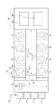
図1に示すように、第1の実施形態に係る基板処理装置10は、複数の開閉ユニット(収納部)11と、第1の搬送ロボット(基板搬送装置)12と、バッファユニット(収納部)13と、第2の搬送ロボット(基板搬送装置)14と、複数の基板処理部15と、装置付帯ユニット16とを備えている。
(Basic configuration)
As shown in FIG. 1, a
各開閉ユニット11は、一列に並べられて設けられている。これらの開閉ユニット11は搬送容器として機能する専用ケース(例えばFOUP)のドアを開閉する。なお、専用ケースがFOUPである場合、開閉ユニット11はFOUPオープナーと呼ばれる。この専用ケースには、基板Wが所定間隔で積層されて収納されている。
The open /
第1の搬送ロボット12は、各開閉ユニット11が並ぶ第1の搬送方向に沿って移動するように各開閉ユニット11の列の隣に設けられている。この第1の搬送ロボット12は、開閉ユニット11によりドアが開けられた専用ケースから未処理の基板Wを取り出す。そして、第1の搬送ロボット12は、必要に応じてバッファユニット13付近まで第1の搬送方向に移動し、停止する。そして、第1の搬送ロボット12は、停止場所で旋回して未処理の基板Wをバッファユニット13に搬入する。また、第1の搬送ロボット12は、バッファユニット13から処理済の基板Wを取り出し、必要に応じて所望の開閉ユニット11付近まで第1の搬送方向に移動し、停止する。そして、第1の搬送ロボット12は、停止場所で旋回して処理済の基板Wを所望の専用ケースに搬入する。なお、第1の搬送ロボット12は、移動せずに旋回し、未処理の基板Wをバッファユニット13に、あるいは、処理済の基板Wを所望の専用ケースに搬入する場合もある。第1の搬送ロボット12としては、例えば、ロボットアームやロボットハンド、移動機構などを有するロボットを用いることが可能である。
The
バッファユニット13は、第1の搬送ロボット12が移動する第1のロボット移動路の中央付近に位置付けられ、その第1のロボット移動路の片側、すなわち各開閉ユニット11と反対の片側に設けられている。このバッファユニット13は、第1の搬送ロボット12と第2の搬送ロボット14との間で基板Wの持ち替えを行うためのバッファ台(基板受渡台)として機能する。このバッファユニット13には、基板Wが所定間隔で積層されて収納される。
The
第2の搬送ロボット14は、バッファユニット13付近から前述の第1の搬送方向に直交する第2の搬送方向(第1の搬送方向に交差する方向の一例)に移動するように設けられている。この第2の搬送ロボット14は、バッファユニット13から未処理の基板Wを取り出し、必要に応じて所望の基板処理部15付近まで第2の搬送方向に沿って移動し、停止する。そして、第2の搬送ロボット14は、停止場所で旋回して未処理の基板Wを所望の基板処理部15に搬入する。また、第2の搬送ロボット14は、基板処理部15から処理済の基板Wを取り出し、必要に応じてバッファユニット13付近まで第2の搬送方向に移動し、停止する。そして、第2の搬送ロボット14は、停止場所で旋回して処理済の基板Wをバッファユニット13に搬入する。なお、第2の搬送ロボット14は、移動せずに旋回し、未処理の基板Wを所望の基板処理部15に、あるいは、処理済の基板Wをバッファユニット13に搬入する場合もある。第2の搬送ロボット14としては、例えば、ロボットアームやロボットハンド、移動機構などを有するロボットを用いることが可能である(詳しくは、後述する)。
The
基板処理部15は、第2の搬送ロボット14が移動する第2のロボット移動路の両側に例えば4つずつ設けられている。基板処理部15は、処理室15aと、基板保持部15bと、第1の処理液供給部15cと、第2の処理液供給部15dとを有する。基板保持部15b、第1の処理液供給部15c及び第2の処理液供給部15dは、処理室15a内に設けられている。
For example, four
処理室15aは、例えば直方体形状に形成され、基板シャッタ15a1を有する。基板シャッタ15a1は、処理室15aにおける第2のロボット移動路側の壁面に開閉可能に形成されている。なお、処理室15a内は、ダウンフロー(垂直層流)によって清浄に保たれており、また、外部よりも陰圧に保持されている。
The
基板保持部15bは、ピン(図示せず)などにより基板Wを水平状態に保持し、基板Wの被処理面の略中央に垂直に交わる軸(基板Wの被処理面に交わる軸の一例)を回転中心として基板Wを水平面内で回転させる機構である。例えば、基板保持部15bは、水平状態に保持した基板Wを回転軸やモータなどを有する回転機構(図示せず)により回転させる。
The
第1の処理液供給部15cは、基板保持部15b上の基板Wの被処理面の中央付近に第1の処理液を供給する。この第1の処理液供給部15cは、例えば、処理液を吐出するノズルを有しており、ノズルを基板保持部15b上の基板Wの被処理面の中央付近に移動させて、そのノズルから処理液を供給する。第1の処理液供給部15cには、第1の処理液が液供給ユニット16aから配管(図示せず)を介して供給される。
The first processing
第2の処理液供給部15dは、基板保持部15b上の基板Wの被処理面の中央付近に第2の処理液を供給する。この第2の処理液供給部15dは、例えば、処理液を吐出するノズルを有しており、ノズルを基板保持部15b上の基板Wの被処理面の中央付近に移動させて、そのノズルから処理液を供給する。第2の処理液供給部15dには、第2の処理液が液供給ユニット16aから配管(図示せず)を介して供給される。
The second processing
装置付帯ユニット16は、第2のロボット移動路の一端、すなわちバッファユニット13と反対側の端に設けられている。この装置付帯ユニット16は、液供給ユニット16aと、制御ユニット(制御部)16bとを収納する。液供給ユニット16aは、各基板処理部15に各種の処理液(例えば、レジスト剥離液やリンス液、洗浄液など)を供給する。制御ユニット16bは、各部を集中的に制御するマイクロコンピュータと、基板処理に関する基板処理情報や各種プログラムなどを記憶する記憶部(いずれも図示せず)を具備する。この制御ユニット16bは、基板処理情報や各種プログラムに基づき、各開閉ユニット11や第1の搬送ロボット12、第2の搬送ロボット14、各基板処理部15などの各部を制御する。
The
(基板搬送装置)
次に、前述の第2の搬送ロボット14について図2から図6を参照して説明する。なお、図3では、第2の搬送ロボット14の把持機構が見えるように示されている。
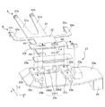
(Substrate transfer device)
Next, the
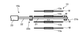
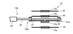
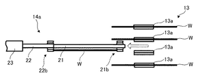
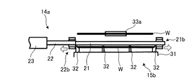
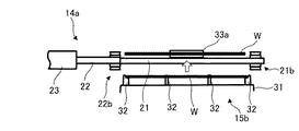
図2及び図3に示すように、第2の搬送ロボット14は、第1のアームユニット14aと、第2のアームユニット14bと、液受けカバー14cと、昇降回転部14dと、移動機構14eとを備えている。この第2の搬送ロボット14は、2台のアームユニット14a、14bを上下二段に有するダブルアームロボットである。第1のアームユニット14a及び第2のアームユニット14bは基本的に同じ構造であるため、代表して第1のアームユニット14aの構造について説明する。
As shown in FIGS. 2 and 3, the
第1のアームユニット14aは、第1の把持板21と、第2の把持板22と、把持部23と、アーム部24とを備えている。第1の把持板21及び第2の把持板22はハンド部として機能する(図4参照)。この第1のアームユニット14aの一部(第1の把持板21、第2の把持板22及び把持部23)と、第2のアームユニット14bの一部(第1の把持板21、第2の把持板22及び把持部23)は上下に位置付けられている。なお、第1のアームユニット14aの各部21〜24について詳しくは後述する。
The
液受けカバー14cは、第1のアームユニット14a及び第2のアームユニット14bを取り囲むように設けられ、各アーム部24の伸縮動作を妨げないように形成されている。この液受けカバー14cが存在するため、処理が終わった後の濡れた状態の基板Wを搬送する場合に基板W上から液が落下して跳ねたとしても、その液は液受けカバー14cに当たる。これにより、基板W上から落下した液が移動機構14eや部屋の床面に飛散することを抑えることができる。
The
昇降回転部14dは、第1のアームユニット14a及び第2のアームユニット14bの各アーム部24を保持して鉛直方向の軸A1に沿って移動させ、第1のアームユニット14a及び第2のアームユニット14bを液受けカバー14cと共に昇降させる。また、昇降回転部14dは、鉛直方向の軸を回転軸(ロボット回転軸)として回転し、保持している各アーム部24を液受けカバー14cと共に回す。この昇降回転部14dは、昇降機構や回転機構(いずれも図示せず)を内蔵している。昇降回転部14dは電気的に制御ユニット16b(図1参照)に接続されており、その駆動が制御ユニット16bにより制御される。なお、昇降回転部14dは昇降部として機能する。
The lifting / lowering
移動機構14eは、図2に示すように、直線レール(移動軸)41と、移動駆動部42とを備えている。直線レール41は、前述の第2の搬送方向に沿って延びるレールである。また、移動駆動部42は、昇降回転部14dを回転可能に支持し、直線レール41に沿って移動可能に直線レール41上に設けられている。移動機構14eは、移動駆動部42により昇降回転部14dを直線レール41に沿って移動させる。この移動機構14eは電気的に制御ユニット16b(図1参照)に接続されており、その駆動が制御ユニット16bにより制御される。
As shown in FIG. 2, the moving
(第1のアームユニット)
次に、第1のアームユニット14aについて詳しく説明する。
(First arm unit)
Next, the
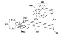
第1の把持板21は、図4に示すように、二本の第1の指部21aを有している。それらの指部21aの先端には、第1の爪部21bが個別に設けられている。この第1の爪部21bは、図5に示すように、基板Wの外周面(側面)に当接する当接面M1(M1a、M1b)を上下に有している。なお、図5では、図4に示すA方向(斜め下方向)から二本の第1の指部21aが示されている。この図5に示すように、第1の爪部21bは、上爪21b1及び下爪21b2により構成されている。上爪21b1は、第1の把持板21の上面(表面)に設けられており、当接面M1aを有している。また、下爪21b2は、第1の把持板21の下面(表面と反対側の裏面)に設けられており、当接面M1bを有している。
As shown in FIG. 4, the
このように第1の爪部21bは、第1の把持板21の水平面(X−Y面)を基準面として、上下(Z方向)に当接面M1(M1a、M1b)を有している。上爪21b1は第1の把持板21の水平面よりも上に設けられ、下爪21b2は第1の把持板21の水平面よりも下に設けられるように第1の把持板21により支持されている。
Thus, the 1st nail | claw
ここで、第1の把持板21の上面(表面)は、基板Wを上側に把持したときに、基板Wの主面(被処理面とは反対側の面)に対向するようにX−Y面に延在している。また、第1の把持板21の下面(表面と反対側の裏面)は、基板Wを下側に把持したときに、基板の主面(表面)に対向するようにX−Y面に延在している。
Here, the upper surface (front surface) of the first
第2の把持板22は、図4に示すように、第1の把持板22に重なるようにその第1の把持板22の上面に設けられている。この第2の把持板22は、第1の把持板21と同様、二本の第2の指部22aを有している。それらの指部22aの先端には、第2の爪部22bが個別に設けられている。この第2の爪部22bは、図6に示すように、基板Wの外周面(側面)に当接する当接面M2(M2a、M2b)を上下に有している。なお、図6では、図4に示すB方向(斜め下方向)から二本の第2の指部22aが示されている。この図6に示すように、第2の爪部22bは、上爪22b1及び下爪22b2が一体に形成された爪ブロックである。上爪22b1及び下爪22b2は、それぞれ当接面M2(M2a、M2b)を有している。この第2の爪部22bは、第2の把持板21の下面(裏面)に設けられている。
As shown in FIG. 4, the
このように第2の爪部22bも、第1の爪部21bと同様に、第1の把持板21の水平面(X−Y面)を基準面として、上下(Z方向)に当接面M2(M2a、M2b)を有している。上爪22b1は第1の把持板21の水平面よりも上に設けられ、下爪22b2は第1の把持板21の水平面よりも下に設けられるように第2の把持板22により支持されている。
As described above, the
把持部23は、図3及び図4に示すように、各第1の爪部21b及び各第2の爪部22bが基板Wの外周面に交わる方向(例えば水平方向)に接離するよう、すなわち近づいたり、離れたりするように、第1の把持板21及び第2の把持板22を相対移動させる。例えば、各第1の爪部21b及び各第2の爪部22bが近づく方向に移動すると、それらの間に位置する基板Wを把持する。このとき、各第1の爪部21b及び各第2の爪部22bの当接面M1(M1a、M1b)及び当接面M2(M2a、M2b)は、基板Wの外周面に当接している。逆に、各第1の爪部21b及び各第2の爪部22bが離れる方向に移動すると、それらの間に位置する基板Wの把持を開放する。
As shown in FIGS. 3 and 4, the
この把持部23は、図4に示すように、支持板23aと、一対のリニアガイド23bと、一対の第1の直動ブロック23cと、一対の第2の直動ブロック23dと、第1の連結板23eと、第2の連結板23fと、エアシリンダ23gと、揺動ピン機構23hとを備えている。
As shown in FIG. 4, the
支持板23aは、アーム部24により保持されている。また、一対のリニアガイド23bは、X方向に延伸するレール状に支持板23a上に設けられている。
The
一対の第1の直動ブロック23cは、一対のリニアガイド23bの延伸方向に移動可能になるように各リニアガイド23b上に個別に設けられている。この一対の第1の直動ブロック23cは、第1の把持板21を移動可能に支持するための部材である。
The pair of first linear motion blocks 23c are individually provided on each
一対の第2の直動ブロック23dは、一対のリニアガイド23bの延伸方向に移動可能になるように各リニアガイド23b上に個別に設けられている。この一対の第2の直動ブロック23dは、第2の把持板22を移動可能に支持するための部材である。
The pair of second
第1の連結板23eは、一対の第1の直動ブロック23cと第1の把持板21とを連結する。また、第2の連結板23fは、一対の第2の直動ブロック23dと第2の把持板22とを連結する。
The first connecting
ここで、第2の連結板23f及び第2の把持板22には、開口サイズが異なる二つの貫通孔H1、H2がY方向に並ぶように形成されている。貫通孔H1のサイズは、貫通孔H2のサイズよりも小さい。
Here, two through holes H1 and H2 having different opening sizes are formed in the second connecting
また、第1の把持板21にも、前述の各貫通孔H1、H2の位置に合せて二つの貫通孔H3、H4が形成されている。これらの貫通孔H3、H4は、前述の各貫通孔H1、H2の開口サイズと逆の開口サイズになるように形成されている。このため、貫通孔H4のサイズは、貫通孔H5のサイズよりも小さい。
The
エアシリンダ23gは、そのロッド(図示せず)が第2の連結板23fの端部に連結されており、第2の連結板23fをX方向にスライド移動させる。このエアシリンダ23gは電気的に制御ユニット16b(図1参照)に接続されており、その駆動が制御ユニット16bにより制御される。
The air cylinder 23g has a rod (not shown) connected to the end of the second connecting
揺動ピン機構23hは、回転体23h1と、二本の揺動ピン23h2とを有している。回転体23h1は、その中心を回転軸として回転可能に支持板23aに設けられている。各揺動ピン23h2は、回転体23h1の回転軸を間として対向する位置に位置付けられ、回転体23h1上に設けられている。これらの揺動ピン23h2は、前述の二つの貫通孔H1及びH3と、もう一方の二つの貫通孔H2及びH4とに個別に通されている。
The
なお、貫通孔H2は、エアシリンダ23gのロッドの所定の移動範囲において、揺動ピン23h2が第2の把持板22及び第2の連結板23fに当接しない孔サイズになるように形成されている。また、貫通孔H3も、エアシリンダ23gのロッドの所定の移動範囲において、揺動ピン23h2が第1の把持板22に当接しないサイズに形成されている。
The through hole H2 is formed so as to have a hole size in which the swing pin 23h2 does not come into contact with the second
ここで、エアシリンダ23gがロッドの所定量の移動によって第2の連結板23f及び一対の第2の直動ブロック23dをスライド移動させると、第2の把持板22が水平方向に移動する。この移動に応じて、揺動ピン機構23hにより第1の把持板21が第2の把持板22の移動方向と逆方向に、第1の連結板23e及び一対の第1の直動ブロック23cと共に移動する。これにより、基板Wを把持あるいは開放する動作を行うことが可能となる。
Here, when the air cylinder 23g slides the second connecting
図3に戻り、アーム部24は、昇降回転部14d上に連結されており、昇降回転部14dにより鉛直方向の軸に沿って昇降可能に形成されている。このアーム部24は伸縮可能に形成されており、把持部23を保持し、保持した把持部23を第1の把持板21及び第2の把持板22と共に水平な直線方向に移動させる。これにより、第1の把持板21及び第2の把持板22は水平方向に移動することになる。第1の把持板21及び第2の把持板22、すなわちハンド部が前進及び後退することで、バッファユニット13や処理室15aに基板Wを搬入したり、それらから基板Wを搬出したりする。
Returning to FIG. 3, the
(基板処理工程)
次に、前述の基板処理装置10が行う基板処理の流れについて説明する。なお、基板Wに対して2種類の処理を行う場合には、図1において、上下に延びる第2のロボット搬送路を挟んで左側の4つの処理室15a(以下、第1の処理室15aとすることがある)と、右側の4つの処理室15a(以下、第2の処理室15aとすることがある)が異なる処理を行うように設定されている。異なる処理を行う場合、第1の処理室は、第1の処理が行われる処理室であり、第2の処理室は、第1の処理の次の処理(第2の処理)が行われる処理室である。
(Substrate processing process)
Next, the flow of substrate processing performed by the above-described
まず、未処理の基板Wが開閉ユニット11内の専用ケースから第1の搬送ロボット12により取り出される。第1の搬送ロボット12は、必要に応じて第1のロボット移動路に沿って移動し、停止する。そして、第1の搬送ロボット12は、停止場所で旋回して未処理の基板Wをバッファユニット13に搬入する。これにより、バッファユニット13には、未処理の基板Wが収納される。
First, the unprocessed substrate W is taken out from the dedicated case in the opening /
その後、バッファユニット13内の未処理の基板Wは、第2の搬送ロボット14により取り出される。第2の搬送ロボット14は、必要に応じて第2のロボット移動路に沿って移動し、停止する。そして、第2の搬送ロボット14は、停止場所で旋回して未処理の基板Wを所望の第1の処理室15aに搬入する。これにより、第1の処理室15a内に未処理の基板Wがセットされる。その後、第1の処理室15aにおいて基板Wに第1の処理が行われる。
Thereafter, the unprocessed substrate W in the
第1の処理室15aでの処理が終了すると、第1の処理室15a内から処理済の基板Wが第2の搬送ロボット14により取り出される。第2の搬送ロボット14は、180°旋回して処理済の基板Wを第2の処理室15aに搬入する。これにより、第2の処理室15a内に処理済の基板Wがセットされる。その後、第2の処理室15aにおいて基板Wに第2の処理が行われる。
When the processing in the
第2の処理室15aでの処理が終了すると、第2の処理室15a内から処理済の基板Wが第2の搬送ロボット14により取り出される。第2の搬送ロボット14は、必要に応じて第2のロボット移動路に沿って移動し、停止する。そして、第2の搬送ロボット14は、停止場所で旋回して処理済の基板Wをバッファユニット13に搬入する。これにより、バッファユニット13には、処理済の基板Wが収納される。
When the processing in the
その後、バッファユニット13内の処理済の基板Wは、第1の搬送ロボット12により取り出される。第1の搬送ロボット12は、必要に応じて第1のロボット移動路に沿って移動し、停止する。そして、第1の搬送ロボット12は、停止場所で旋回して処理済の基板Wを所望の専用ケースに搬入する。これにより、専用ケースには、処理済の基板Wが収納される。
Thereafter, the processed substrate W in the
(第2の搬送ロボットによる基板搬送工程)
次いで、前述の基板処理工程において、第2の搬送ロボット14が行う基板搬送の流れについて図7から図12を参照して詳しく説明する。まず、第2の搬送ロボット14とバッファユニット13との基板Wの受け渡しについて説明する。
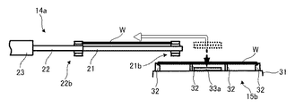
(Substrate transfer process by the second transfer robot)
Next, the flow of substrate transfer performed by the
図7から図12に示すように、バッファユニット13には、基板Wを所定間隔で積層して収納するための置台部材13aが高さ方向に所定間隔で設けられている。これらの置台部材13aは水平面内で対向するように位置付けられており、同じ高さ位置に存在する一対の置台部材13aが互いに基板Wの外周の一部を支持して一枚の基板Wを保持する。この一対の置台部材13aには、第1のアームユニット14a又は第2のアームユニット14bにより上方から基板Wが載置される。
As shown in FIGS. 7 to 12, the
バッファユニット13は、1以上の未処理の基板Wと、1以上の処理済の基板Wが載置されることが可能になっている。本実施形態の場合には、第1のアームユニット14a又は第2のアームユニット14bの侵入位置より上方の置台部材13aに処理済の基板Wが載置されるように、その侵入位置より上方は空き状態となっている。一方、第1のアームユニット14a又は第2のアームユニット14bの侵入位置より下方の置台部材13aには、未処理の基板Wが載置されている。
The
図7に示すように、バッファユニット13に対する処理済の基板Wの搬送では、処理済の基板Wを上側(各上爪21b1、各上爪22b1)に保持する第1のアームユニット14aにより、処理済の基板Wがバッファユニット13の一対の置台部材13a上に載置される。次いで、図8に示すように、第1のアームユニット14aによる把持が開放され、処理済の基板Wが一対の置台部材13aにより支持される。その後、図9に示すように、第1のアームユニット14aは、一対の置台部材13a上の未処理の基板Wを把持する把持位置まで下降する。そして、図10に示すように、把持位置まで下降した第1のアームユニット14aは、一対の置台部材13a上の未処理の基板Wを下側(各下爪21b2、各下爪22b2)で把持する。次いで、図11に示すように、未処理の基板Wを下側に保持した第1のアームユニット14aは、退避できるように水平移動可能な位置まで所定距離だけ上昇する。そして、図12に示すように、未処理の基板Wを下側に保持した第1のアームユニット14aは、高さ方向の各置台部材13aの間から退避し、バッファユニット13から未処理の基板Wを取り出す。このようにして、第1のアームユニット14aは、処理済の基板Wと未処理の基板Wを持ち替えることができる。
As shown in FIG. 7, in the transfer of the processed substrate W to the
次に、第2の搬送ロボット14と処理室15a(第1の処理室15a及び第2の処理室15a)との基板Wの受け渡しについて説明する。
Next, transfer of the substrate W between the
基板Wを把持していない第1のアームユニット14aは、バッファユニット13から未処理の基板Wを下側(各下爪21b2、各下爪22b2)で取り出し、第1の処理室15aに向かう。また、第1の処理室15aでは、基板Wを把持していない第2のアームユニット14bは、第1の処理室15aから第1の処理が行われた処理済の基板Wを下側(各下爪21b2、各下爪22b2)又は上側(各上爪21b1、各上爪22b1)で把持して取り出す。そして、未処理の基板Wを下側に保持した第1のアームユニット14aは、第1の処理室15aに未処理の基板Wをセットする。
The
処理済の基板Wを下側(各下爪21b2、各下爪22b2)又は上側(各上爪21b1、各上爪22b1)に保持した第2のアームユニット14bは、180度旋回し、第1の処理室15aに対向する第2の処理室15aに向かう。第2の処理室15aでは、まず、基板Wを把持していない第1のアームユニット14aは、第2の処理室15aから第2の処理が行われた処理済の基板Wを上側(各上爪21b1、各上爪22b1)で把持して取り出す。そして、第1の処理室15aによる処理済の基板Wを下側(各下爪21b2、各下爪22b2)又は上側(各上爪21b1、各上爪22b1)に保持した第2のアームユニット14bは、第1の処理室15aによる処理済の基板Wを第2の処理室15aにセットする。
The
このような基板搬送工程において、バッファユニット13に対する処理済の基板Wの搬送では、第1のアームユニット14aはバッファユニット13に移動し、アーム部24を伸ばして処理済の基板Wをバッファユニット13に置く。そして、第1のアームユニット14aは下降して、次の未処理の基板Wを下側(各下爪21b2、各下爪22b2)で把持する。このように、第1のアームユニット14aは、処理済の基板Wをバッファユニット13に載置した後、アーム部24の水平位置を変えず、未処理の基板Wを把持する高さまで下降し、未処理の基板Wを把持してからアーム部24を縮めることが可能である。これにより、第1のアームユニット14aの出し入れ、すなわちハンドの出し入れが従来の二回に比べて一回となって省略されるので、基板搬送時間を短縮することができる。また、アーム部24の水平位置を変えずに処理済の基板Wと未処理の基板Wの交換が行えるので、水平位置合わせを行う必要がなく、把持部23の制御を簡略にし、基板搬送時間を短縮することができる。したがって、基板処理装置10の基板処理枚数を増やすことが可能となり、その生産性を向上させることができる。なお、第2の搬送ロボット14によれば、基板Wの把持を4カ所(第1のアームユニット14aの上側及び下側、第2のアームユニット14bの上側及び下側)で行うことができる。
In such a substrate transporting process, in transporting the processed substrate W to the
また、1つの第1のアームユニット14aの上側及び下側において基板Wの把持を行うことができるので、未処理の基板Wを把持する側の部材(爪やハンド部の水平面)と処理済の基板Wを把持する側の部材(爪やハンド部の水平面)を分離することができる。そのため、未処理の基板Wに付着した汚染物質(パーティクル)が、第1のアームユニット14aを介して処理済の基板Wに付着することを抑止することができる。さらに、未処理の基板Wを下側で把持し、処理済の基板を上側で把持するので、未処理の基板Wに付着している汚染物質が重力落下によって下の処理済の基板Wに付着することを抑止することができる。以上により、基板搬送時間の短縮化を図りつつ、処理済の基板Wを清浄に保ちながら基板Wをバッファユニット13に搬送することができる。
In addition, since the substrate W can be gripped on the upper side and the lower side of the
以上説明したように、第1の実施形態によれば、基板Wの外周面に当接する当接面M1(M1a、M1b)を上下に有する第1の爪部21bと、その第1の爪部21bを支持する第1の把持板21と、基板Wの外周面に当接する当接面M2(M2a、M2b)を上下に有する第2の爪部22bと、第1の把持板21及び第2の把持板22を水平方向に相対移動させる把持部23とを設けることによって、第1の把持板21及び第2の把持板22のハンドの両面(上側及び下側)に基板を保持することが可能となる。例えば、処理済の基板Wを上側に保持したハンドは、処理済の基板Wをバッファユニット13に置き、そのまま、下降して次の未処理の基板Wを下側で把持することができる。これにより、ハンドの出し入れが通常の二回に比べ一回となって省略されるので、基板搬送時間を短縮することができる。
As described above, according to the first embodiment, the
<第2の実施形態>
第2の実施形態について図13から図19を参照して説明する。なお、第2の実施形態では、第1の実施形態との相違点(基板昇降部)について説明し、その他の説明を省略する。
<Second Embodiment>
A second embodiment will be described with reference to FIGS. In the second embodiment, the difference (substrate lifting part) from the first embodiment will be described, and the other description will be omitted.
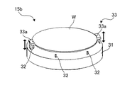
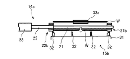
図13に示すように、第2の実施形態に係る基板保持部15bは、基板処理台31と、複数の支持部材32と、基板昇降部33とを備えている。この基板保持部15bは、第1の実施形態と同様、基板処理部15の処理室15a内に設けられている。
As shown in FIG. 13, the
各支持部材32は、基板Wを下面から支持する。これらの支持部材32は、例えば円環状に位置付けられ、基板処理台31の表面に設けられている。
Each
基板昇降部33は、各支持部材32よりも外側から基板Wを支持可能となるような配置で基板処理台31に設けられている。この基板昇降部33は、基板Wを支持する複数(図13の例では、二つ)の昇降部材33aを有している。これらの昇降部材33aは昇降方向に移動可能に形成されている。これにより、各支持部材32により支持された基板Wは、各昇降部材33aの昇降に応じ、各昇降部材33aにより保持されて昇降方向に移動することになる。
The
なお、基板昇降部33は、各支持部材32よりも外側から基板Wを支持可能となる位置であれば、基板処理台31上に設けられていなくてもよく、基板処理台31の外方に設けられることも可能である。この場合には、基板昇降部33を基板処理部15の底部に設けることができる。
The
この基板保持部15bでは、基板Wの受け渡し時、処理済の基板Wは基板昇降部33により保持されて所定の最高の高さ位置まで移動する。これにより、処理済の基板Wの下方に第1のアームユニット14aが入り込むことが可能になるので、処理室15a内において第1のアームユニット14aだけで基板Wを交換することが可能となる。なお、前述の第1の実施形態では、処理室15a内の処理済の基板Wを片方の第2のアームユニット14bで取り出し、他方の第1のアームユニット14aで未処理の基板Wをセットする交換動作を行う。
In the
(第2の搬送ロボットによる基板搬送工程)
次に、第2の搬送ロボット14と処理室15aとの基板Wの受け渡しについて図14から図19を参照して説明する。
(Substrate transfer process by the second transfer robot)
Next, transfer of the substrate W between the
図14に示すように、処理室15aに対する処理済の基板Wの搬送では、処理済の基板Wを保持する基板保持部15bの各昇降部材33aが上昇し、昇降部材33aの上端面と支持部材32の上端面との間に第1のアームユニット14aが挿入可能な位置まで移動する。そして、昇降部材33aの上端面と支持部材32の上端面との間に高さが位置付けられた第1のアームユニット14aは、昇降部材33aの上端面と支持部材32の上端面との間に侵入し、基板処理台31上で停止する。このとき、第1のアームユニット14aは、未処理の基板Wを下側(各下爪21b2、各下爪22b2)に把持している。
As shown in FIG. 14, in the transfer of the processed substrate W to the
その後、図15に示すように、未処理の基板Wを下側に保持する第1のアームユニット14aにより、未処理の基板Wが処理室15aの各支持部材32上に載置される。次いで、図16に示すように、第1のアームユニット14aによる把持が開放され、未処理の基板Wが各支持部材32により支持される。その後、図17に示すように、第1のアームユニット14aは、一対の昇降部材33a上の処理済の基板Wを把持する把持位置まで上昇する。そして、図18に示すように、把持位置まで上昇した第1のアームユニット14aは、一対の昇降部材33a上の処理済の基板Wを把持する。次いで、図19に示すように、一対の昇降部材33aが下降すると、処理済の基板Wを上側に保持した第1のアームユニット14aは、基板保持部15b上から退避し、処理室15aから未処理の基板Wを取り出す。このようにして、第1のアームユニット14aは、未処理の基板Wと処理済の基板Wを持ち替えることができる。
After that, as shown in FIG. 15, the unprocessed substrate W is placed on each
この基板搬送工程によれば、第1のアームユニット14aは未処理の基板Wを下側で把持し、処理室15aの基板処理台31上まで移動し、未処理の基板Wを基板処理台31の各支持部材32上にセットする。その後、第1のアームユニット14aは、基板Wを把持していない状態で、そのまま処理済の基板Wを把持する把持位置まで上昇する。そして、第1のアームユニット14aは処理済の基板Wを上側で把持し、処理室15aから取り出す。これにより、第1のアームユニット14aの出し入れ、すなわちハンドの出し入れが従来の二回に比べて一回となって省略されるので、基板搬送時間を短縮することができる。したがって、基板処理装置10の基板処理枚数を増やすことが可能となり、その生産性を向上させることができる。
According to this substrate transport process, the
また、1つの第1のアームユニット14aの上側及び下側において基板Wの把持を行うことができるので、未処理の基板Wを把持する側の部材(爪やハンド部の水平面)と処理済の基板Wを把持する側の部材(爪やハンド部の水平面)を分離することができる。このため、未処理の基板Wに付着した汚染物質(パーティクル)が、第1のアームユニット14aを介して処理済の基板Wに付着することを抑止することができる。さらに、未処理の基板Wを下側で把持し、処理済の基板を上側で把持するので、未処理の基板Wに付着している汚染物質が重力落下によって下の処理済の基板Wに付着することを抑止することができる。以上により、基板搬送時間の短縮化を図りつつ、処理済の基板Wを清浄に保ちながら基板Wをバッファユニット13に搬送することができる。
In addition, since the substrate W can be gripped on the upper side and the lower side of the
以上説明したように、第2の実施形態によれば、第1の実施形態と同様の効果を得ることができる。さらに、処理室15aに基板昇降部33を設けることによって、バッファユニット13及び処理室15aの両方で、1つのアームユニット14a、14bによる基板交換を実現することが可能となるので、より基板搬送時間を短縮することができる。
As described above, according to the second embodiment, the same effect as that of the first embodiment can be obtained. Furthermore, by providing the substrate lifting / lowering
<他の実施形態>
前述の各実施形態においては、上下のアームユニット14a、14bの両方に上下爪(第1の爪部21b及び第2の爪部22b)を適用することを例示したが、これに限るものではなく、例えば、上のアームユニット14aの片方だけに適用することも可能である。また、第1の爪部21b及び第2の爪部22bを同じ構造することも可能であり、第2の搬送ロボット14の構造を第1の搬送ロボット12に適用することも可能である。上下爪(第1の爪部21b及び第2の爪部22b)は二つ以上であればよく、その数は特に限定されるものではない。
<Other embodiments>
In each of the above-described embodiments, the upper and lower claws (the
また、前述の各実施形態においては、第1の把持板21及び第2の把持板22の両方を移動させることを例示したが、これに限るものではなく、例えば、第1の把持板21及び第2の把持板22のどちらか一方だけを移動させるようにしてもよい。
Further, in each of the above-described embodiments, it is exemplified that both the first
また、前述の各実施形態においては、二種類の処理室15aを用いることを例示したが、これに限るものではなく、例えば、三種類の処理室15aを用いるようにしてもよい。この場合には、処理1→処理2→処理3の順に処理を行ってからバッファユニット13に処理済の基板Wを戻す作業になる。例えば、処理2を行う処理室15aの数を4つにするが、これは、処理2を行う処理室15aの処理が処理1又は処理3に比べて2倍の時間を要することを想定し、台数を倍に設定しているためである。また、一種類の処理室15aを用いるようにしてもよい。この場合には、処理1の処理が終了次第、バッファユニット13に処理済みの基板Wを戻す作業になる。
In the above-described embodiments, the use of two types of
また、前述の実施形態においては、上側で処理済の基板Wを把持し、下側で未処理の基板Wを把持するようにしたが、これに限るものではなく、逆にしてもよい。すなわち、上側で未処理の基板Wを把持し、下側で処理済の基板Wを把持する。この場合には、バッファユニット13にアームユニット14a、14bを挿入する高さ位置よりも上側の置台部材13aに未処理の基板Wを載置し、下側の置台部材13aに処理済の基板Wを載置することができる。また、基板昇降部33に未処理の基板Wを載置し、各支持部材32から処理済の基板Wを取り出し、その後に基板昇降部33を下降させて各支持部材32に未処理の基板Wを受け渡すことができる。
In the above-described embodiment, the processed substrate W is gripped on the upper side, and the unprocessed substrate W is gripped on the lower side. However, the present invention is not limited to this and may be reversed. That is, the unprocessed substrate W is gripped on the upper side, and the processed substrate W is gripped on the lower side. In this case, the unprocessed substrate W is mounted on the mounting
また、前述の実施形態においては、第2のアームユニット14bは、第1のアームユニット14aと同じ構造としたが、処理室15aで行われる処理の種類が少ない場合(例えば2つ以下の場合)には、処理室15a間での基板Wの搬送を行う第2のアームユニット14bは、上側(各上爪21b1、各上爪22b1)又は下側(各下爪21b2、各下爪22b2)の一方のみで把持を行うものであってもよい。この場合には、使用しない他方の爪部を適宜省略することができる。
In the above-described embodiment, the
また、前述の実施形態においては、昇降回転部14dによって第1のアームユニット14a及び第2のアームユニット14bを昇降させることで、バッファユニット13の置台部材13aに基板Wを載置、または、置台部材13aから基板Wを取り出しできるようにしたが、これに限るものではなく、バッファユニット13に積層される基板Wの積層方向(一対の置台部材13aの配列方向)に対して、各アームユニット14a、14bが相対的に位置を変えられるようにすればよい。例えば、バッファユニット13に昇降部を設け、バッファユニット13を基板Wの積層方向に昇降させるようにしてもよい。この場合、バッファユニット13は、基板Wの載置、取り出しのときの前述したアームユニット14a、14bの昇降動作とは逆方向の昇降動作を行う。また、この場合、前述の実施形態における、各アームユニット14a、14bを昇降させる昇降部を省略することができる。
In the above-described embodiment, the
以上、本発明のいくつかの実施形態を説明したが、これらの実施形態は、例として提示したものであり、発明の範囲を限定することは意図していない。これら新規な実施形態は、その他の様々な形態で実施されることが可能であり、発明の要旨を逸脱しない範囲で、種々の省略、置き換え、変更を行うことができる。これら実施形態やその変形は、発明の範囲や要旨に含まれるとともに、特許請求の範囲に記載された発明とその均等の範囲に含まれる。 As mentioned above, although some embodiment of this invention was described, these embodiment is shown as an example and is not intending limiting the range of invention. These novel embodiments can be implemented in various other forms, and various omissions, replacements, and changes can be made without departing from the scope of the invention. These embodiments and modifications thereof are included in the scope and gist of the invention, and are included in the invention described in the claims and the equivalents thereof.
10 基板処理装置
11 開閉ユニット
12 第1の搬送ロボット
13 バッファユニット
14 第2の搬送ロボット
14d 昇降回転部
15 基板処理部
16b 制御ユニット
21 第1の把持板
21b 第1の爪部
22 第2の把持板
22b 第2の爪部
23 把持部
33 基板昇降部
21b1 上爪
21b2 下爪
M1a 当接面
M1b 当接面
M2a 当接面
M2b 当接面
W 基板
DESCRIPTION OF
Claims (6)
前記第1の把持板により支持され、基板の外周面に当接する当接面を前記第1の把持板の表面に対して上下に有する第1の爪部と、
前記第1の把持板に重なるように設けられた第2の把持板と、
前記第2の把持板により支持され、前記基板の外周面に当接する当接面を前記第1の把持板の表面に対して上下に有する第2の爪部と、
前記第1の爪部及び前記第2の爪部が前記基板の外周面に交わる方向に接離するように、前記第1の把持板及び前記第2の把持板を相対移動させる把持部と、
を備えることを特徴とする基板搬送装置。 A first gripping plate;
A first claw portion that is supported by the first gripping plate and has a contact surface that contacts the outer peripheral surface of the substrate above and below the surface of the first gripping plate;
A second gripping plate provided to overlap the first gripping plate;
A second claw portion that is supported by the second gripping plate and has a contact surface that contacts the outer peripheral surface of the substrate above and below the surface of the first gripping plate;
A gripper for moving the first gripping plate and the second gripping plate relative to each other so that the first pawl portion and the second pawl portion are in contact with and away from each other in a direction intersecting the outer peripheral surface of the substrate;
A substrate transfer apparatus comprising:
前記第1の把持板の上面に設けられ、前記当接面を有する上爪と、
前記第1の把持板の下面に設けられ、前記当接面を有する下爪と、
を有することを特徴とする請求項1に記載の基板搬送装置。 The first nail portion is
An upper claw provided on the upper surface of the first gripping plate and having the contact surface;
A lower claw provided on the lower surface of the first holding plate and having the contact surface;
The substrate transfer apparatus according to claim 1, comprising:
所定間隔で積層された複数の基板のうち第1の基板を把持する第1の高さ位置から、前記第1の基板の上又は下に位置する第2の基板を把持する第2の高さ位置に前記第1の爪部及び前記第2の爪部を位置付けるよう、前記昇降部に前記把持部の上昇又は下降を実行させ、前記把持部に前記第1の把持板及び前記第2の把持板の相対移動を実行させる制御部と、
をさらに備えることを特徴とする請求項1又は請求項2に記載の基板搬送装置。 An elevating part for elevating and lowering the grip part;
A second height for gripping a second substrate positioned above or below the first substrate from a first height position for gripping the first substrate among a plurality of substrates stacked at a predetermined interval. In order to position the first claw part and the second claw part at a position, the elevating part performs raising or lowering of the grip part, and the grip part has the first grip plate and the second grip. A control unit for performing relative movement of the plate;
The substrate transfer apparatus according to claim 1, further comprising:
請求項1から請求項3のいずれか一項に記載の基板搬送装置と、
前記基板を処理する基板処理部と、
を備えることを特徴とする基板処理装置。 A storage unit that stores a plurality of substrates stacked at predetermined intervals; and
The substrate transfer apparatus according to any one of claims 1 to 3,
A substrate processing unit for processing the substrate;
A substrate processing apparatus comprising:
前記収納部から取り出された前記第1の基板に処理を行う工程と、
前記処理が行われた前記第1の基板を、前記基板搬送装置を用いて前記収納部に収納する工程と、
前記収納部に収納された前記第1の基板の上又は下に位置する第2の基板を、前記基板搬送装置を用いて前記収納部から取り出す工程と、
前記収納部から取り出された前記第2の基板に処理を行う工程と、
前記処理が行われた前記第2の基板を、前記基板搬送装置を用いて前記収納部に収納する工程と、
を有することを特徴とする基板処理方法。 A step of taking out the first substrate using the substrate transfer device according to any one of claims 1 to 3, from a storage unit that stores a plurality of substrates stacked at predetermined intervals.
Processing the first substrate taken out of the storage unit;
Storing the first substrate subjected to the processing in the storage unit using the substrate transfer device;
Removing the second substrate positioned above or below the first substrate stored in the storage unit from the storage unit using the substrate transfer device;
Processing the second substrate taken out of the storage unit;
Storing the second substrate on which the processing has been performed in the storage unit using the substrate transfer device;
A substrate processing method comprising:
Priority Applications (9)
| Application Number | Priority Date | Filing Date | Title |
|---|---|---|---|
| JP2016073092A JP2017183665A (en) | 2016-03-31 | 2016-03-31 | Substrate carrier device, substrate processing apparatus, and substrate processing method |
| TW106107232A TWI685051B (en) | 2016-03-31 | 2017-03-06 | Substrate transfer device, substrate processing device |
| TW109101226A TWI796544B (en) | 2016-03-31 | 2017-03-06 | Substrate transfer device, substrate processing method, and substrate processing device |
| KR1020170039109A KR101962009B1 (en) | 2016-03-31 | 2017-03-28 | Substrate transport apparatus, substrate processing apparatus and substrate processing method |
| US15/472,671 US10483151B2 (en) | 2016-03-31 | 2017-03-29 | Substrate transfer apparatus, substrate processing apparatus, and substrate processing method |
| CN202110213053.1A CN112951750B (en) | 2016-03-31 | 2017-03-31 | Substrate conveying device, substrate processing device and substrate processing method |
| CN201710206582.2A CN107275270B (en) | 2016-03-31 | 2017-03-31 | Substrate conveying device, substrate processing device and substrate processing method |
| KR1020190030394A KR102227108B1 (en) | 2016-03-31 | 2019-03-18 | Substrate transport apparatus, substrate processing apparatus and substrate processing method |
| JP2020113252A JP6970787B2 (en) | 2016-03-31 | 2020-06-30 | Board transfer device and board processing device |
Applications Claiming Priority (1)
| Application Number | Priority Date | Filing Date | Title |
|---|---|---|---|
| JP2016073092A JP2017183665A (en) | 2016-03-31 | 2016-03-31 | Substrate carrier device, substrate processing apparatus, and substrate processing method |
Related Child Applications (1)
| Application Number | Title | Priority Date | Filing Date |
|---|---|---|---|
| JP2020113252A Division JP6970787B2 (en) | 2016-03-31 | 2020-06-30 | Board transfer device and board processing device |
Publications (2)
| Publication Number | Publication Date |
|---|---|
| JP2017183665A true JP2017183665A (en) | 2017-10-05 |
| JP2017183665A5 JP2017183665A5 (en) | 2019-03-07 |
Family
ID=59961904
Family Applications (1)
| Application Number | Title | Priority Date | Filing Date |
|---|---|---|---|
| JP2016073092A Pending JP2017183665A (en) | 2016-03-31 | 2016-03-31 | Substrate carrier device, substrate processing apparatus, and substrate processing method |
Country Status (5)
| Country | Link |
|---|---|
| US (1) | US10483151B2 (en) |
| JP (1) | JP2017183665A (en) |
| KR (2) | KR101962009B1 (en) |
| CN (2) | CN107275270B (en) |
| TW (2) | TWI796544B (en) |
Cited By (1)
| Publication number | Priority date | Publication date | Assignee | Title |
|---|---|---|---|---|
| JP2021166218A (en) * | 2020-04-06 | 2021-10-14 | 信越半導体株式会社 | Robot hand |
Families Citing this family (3)
| Publication number | Priority date | Publication date | Assignee | Title |
|---|---|---|---|---|
| JP7023094B2 (en) * | 2017-12-05 | 2022-02-21 | 日本電産サンキョー株式会社 | robot |
| CN111348427B (en) * | 2020-03-13 | 2022-04-22 | 北京北方华创微电子装备有限公司 | Mechanical arm |
| CN117690858B (en) * | 2024-02-02 | 2024-05-03 | 深圳市森美协尔科技有限公司 | Manipulator assembly and probe station |
Citations (7)
| Publication number | Priority date | Publication date | Assignee | Title |
|---|---|---|---|---|
| JPH0193736U (en) * | 1987-12-12 | 1989-06-20 | ||
| JPH0263990U (en) * | 1988-10-31 | 1990-05-14 | ||
| US20020071756A1 (en) * | 2000-12-13 | 2002-06-13 | Gonzalez Jose R. | Dual wafer edge gripping end effector and method therefor |
| JP2003289094A (en) * | 2002-03-28 | 2003-10-10 | Dainippon Screen Mfg Co Ltd | Substrate transfer method, substrate transfer device, and substrate transfer arm |
| JP2006041423A (en) * | 2004-07-30 | 2006-02-09 | Hitachi Naka Electronics Co Ltd | Transport device for precision thin-sheet material |
| JP2009160711A (en) * | 2008-01-10 | 2009-07-23 | Yaskawa Electric Corp | End effector and transfer device equipped with the same |
| JP2010232349A (en) * | 2009-03-26 | 2010-10-14 | Dainippon Screen Mfg Co Ltd | Substrate processing apparatus and substrate delivery method |
Family Cites Families (21)
| Publication number | Priority date | Publication date | Assignee | Title |
|---|---|---|---|---|
| JPS5823742B2 (en) | 1974-05-31 | 1983-05-17 | 松下電器産業株式会社 | Kingokinmakuno Etsuchinghouhou |
| JPS5852615B2 (en) | 1981-08-05 | 1983-11-24 | レオン自動機株式会社 | Continuous belt-shaped dough discharge device |
| US5700046A (en) * | 1995-09-13 | 1997-12-23 | Silicon Valley Group, Inc. | Wafer gripper |
| JP3745064B2 (en) * | 1997-01-23 | 2006-02-15 | 大日本スクリーン製造株式会社 | Substrate transfer device, substrate transfer method using the same, and substrate attitude conversion device |
| TWI262165B (en) * | 2002-10-16 | 2006-09-21 | Sez Ag | Device and method for transporting wafer-shaped articles |
| JP2006313865A (en) * | 2005-05-09 | 2006-11-16 | Tatsumo Kk | Substrate holder |
| CN1895974A (en) * | 2005-07-15 | 2007-01-17 | 日本电产三协株式会社 | Substrate move-out move-in method and system |
| JP4999487B2 (en) * | 2007-02-15 | 2012-08-15 | 大日本スクリーン製造株式会社 | Substrate processing equipment |
| US9050634B2 (en) * | 2007-02-15 | 2015-06-09 | SCREEN Holdings Co., Ltd. | Substrate processing apparatus |
| JP5548430B2 (en) * | 2008-11-26 | 2014-07-16 | 株式会社日立国際電気 | Substrate processing apparatus and semiconductor device manufacturing method |
| JP2010126797A (en) * | 2008-11-28 | 2010-06-10 | Tokyo Electron Ltd | Film deposition system, semiconductor fabrication apparatus, susceptor for use in the same, program and computer readable storage medium |
| JP5083339B2 (en) * | 2010-02-04 | 2012-11-28 | 東京エレクトロン株式会社 | Substrate transport apparatus, substrate transport method, and storage medium |
| JP5823742B2 (en) * | 2010-07-02 | 2015-11-25 | 芝浦メカトロニクス株式会社 | Gripping device, transport device, processing device, and electronic device manufacturing method |
| JP5728770B2 (en) * | 2011-02-03 | 2015-06-03 | 株式会社昭和真空 | Substrate processing apparatus, substrate processing method, and program |
| JP5709592B2 (en) * | 2011-03-08 | 2015-04-30 | 東京エレクトロン株式会社 | Substrate transport method, recording medium recording a program for executing the substrate transport method, and substrate transport apparatus |
| KR101311616B1 (en) * | 2011-08-12 | 2013-09-26 | 시바우라 메카트로닉스 가부시끼가이샤 | Processing system and processing method |
| JP5582152B2 (en) | 2012-02-03 | 2014-09-03 | 東京エレクトロン株式会社 | Substrate transport apparatus, substrate transport method, and storage medium |
| JP5993625B2 (en) * | 2012-06-15 | 2016-09-14 | 株式会社Screenホールディングス | Substrate reversing apparatus and substrate processing apparatus |
| JP6091867B2 (en) * | 2012-12-04 | 2017-03-08 | 株式会社ディスコ | Transport mechanism |
| JP2016127086A (en) * | 2014-12-26 | 2016-07-11 | 東京エレクトロン株式会社 | Substrate adsorption auxiliary member and substrate feeding device |
| KR102066044B1 (en) * | 2016-06-30 | 2020-02-11 | 세메스 주식회사 | Substrate treating apparatus, index robot and substrate transferring method |
-
2016
- 2016-03-31 JP JP2016073092A patent/JP2017183665A/en active Pending
-
2017
- 2017-03-06 TW TW109101226A patent/TWI796544B/en active
- 2017-03-06 TW TW106107232A patent/TWI685051B/en active
- 2017-03-28 KR KR1020170039109A patent/KR101962009B1/en active IP Right Grant
- 2017-03-29 US US15/472,671 patent/US10483151B2/en active Active
- 2017-03-31 CN CN201710206582.2A patent/CN107275270B/en active Active
- 2017-03-31 CN CN202110213053.1A patent/CN112951750B/en active Active
-
2019
- 2019-03-18 KR KR1020190030394A patent/KR102227108B1/en active IP Right Grant
Patent Citations (7)
| Publication number | Priority date | Publication date | Assignee | Title |
|---|---|---|---|---|
| JPH0193736U (en) * | 1987-12-12 | 1989-06-20 | ||
| JPH0263990U (en) * | 1988-10-31 | 1990-05-14 | ||
| US20020071756A1 (en) * | 2000-12-13 | 2002-06-13 | Gonzalez Jose R. | Dual wafer edge gripping end effector and method therefor |
| JP2003289094A (en) * | 2002-03-28 | 2003-10-10 | Dainippon Screen Mfg Co Ltd | Substrate transfer method, substrate transfer device, and substrate transfer arm |
| JP2006041423A (en) * | 2004-07-30 | 2006-02-09 | Hitachi Naka Electronics Co Ltd | Transport device for precision thin-sheet material |
| JP2009160711A (en) * | 2008-01-10 | 2009-07-23 | Yaskawa Electric Corp | End effector and transfer device equipped with the same |
| JP2010232349A (en) * | 2009-03-26 | 2010-10-14 | Dainippon Screen Mfg Co Ltd | Substrate processing apparatus and substrate delivery method |
Cited By (2)
| Publication number | Priority date | Publication date | Assignee | Title |
|---|---|---|---|---|
| JP2021166218A (en) * | 2020-04-06 | 2021-10-14 | 信越半導体株式会社 | Robot hand |
| JP7287332B2 (en) | 2020-04-06 | 2023-06-06 | 信越半導体株式会社 | robot hand |
Also Published As
| Publication number | Publication date |
|---|---|
| US20170287767A1 (en) | 2017-10-05 |
| KR101962009B1 (en) | 2019-03-25 |
| CN107275270A (en) | 2017-10-20 |
| KR20190031462A (en) | 2019-03-26 |
| KR102227108B1 (en) | 2021-03-15 |
| KR20170113317A (en) | 2017-10-12 |
| CN112951750B (en) | 2024-02-27 |
| TW202022976A (en) | 2020-06-16 |
| TW201738995A (en) | 2017-11-01 |
| US10483151B2 (en) | 2019-11-19 |
| TWI796544B (en) | 2023-03-21 |
| TWI685051B (en) | 2020-02-11 |
| CN107275270B (en) | 2021-03-09 |
| CN112951750A (en) | 2021-06-11 |
Similar Documents
| Publication | Publication Date | Title |
|---|---|---|
| KR102227108B1 (en) | Substrate transport apparatus, substrate processing apparatus and substrate processing method | |
| JP7246147B2 (en) | SUBSTRATE PROCESSING APPARATUS AND SUBSTRATE PROCESSING METHOD | |
| KR20080061290A (en) | Substrate transporting apparatus, substrate platform shelf and substrate processing apparatus | |
| KR20100109357A (en) | Substrate processing apparatus and substrate transport method | |
| JP2018098301A (en) | Substrate processing apparatus | |
| CN107017182A (en) | Substrate processing apparatus | |
| KR102164067B1 (en) | Substrate processing apparatus and substrate processing method | |
| JP2017183666A (en) | Substrate carrier device, substrate processing apparatus and substrate processing method | |
| KR102116344B1 (en) | Substrate processing apparatus and substrate processing method | |
| KR20200083233A (en) | Substrate processing apparatus and substrate transporting method | |
| US20160351434A1 (en) | Substrate conveying system and method | |
| JP5524304B2 (en) | Substrate transport method in substrate processing apparatus | |
| JP7137408B2 (en) | SUBSTRATE PROCESSING APPARATUS AND SUBSTRATE PROCESSING METHOD | |
| TWI529843B (en) | Substrate processing apparatus | |
| JP6970787B2 (en) | Board transfer device and board processing device | |
| JP6144236B2 (en) | Substrate processing method, storage medium, and substrate processing apparatus | |
| JP5385965B2 (en) | Substrate processing equipment | |
| JP5283770B2 (en) | Substrate transport apparatus and substrate processing apparatus provided with the same | |
| JP2008100802A (en) | Substrate storage warehouse | |
| JP5305948B2 (en) | Substrate processing equipment | |
| JP2005311169A (en) | Equipment and method for substrate transfer processing | |
| JP2013131529A (en) | Substrate processing device, and method of manufacturing semiconductor device |
Legal Events
| Date | Code | Title | Description |
|---|---|---|---|
| A521 | Request for written amendment filed |
Free format text: JAPANESE INTERMEDIATE CODE: A523 Effective date: 20190123 |
|
| A621 | Written request for application examination |
Free format text: JAPANESE INTERMEDIATE CODE: A621 Effective date: 20190123 |
|
| A131 | Notification of reasons for refusal |
Free format text: JAPANESE INTERMEDIATE CODE: A131 Effective date: 20190924 |
|
| A977 | Report on retrieval |
Free format text: JAPANESE INTERMEDIATE CODE: A971007 Effective date: 20190919 |
|
| A521 | Request for written amendment filed |
Free format text: JAPANESE INTERMEDIATE CODE: A523 Effective date: 20191125 |
|
| A02 | Decision of refusal |
Free format text: JAPANESE INTERMEDIATE CODE: A02 Effective date: 20200331 |
|
| RD03 | Notification of appointment of power of attorney |
Free format text: JAPANESE INTERMEDIATE CODE: A7423 Effective date: 20200626 |
|
| A521 | Request for written amendment filed |
Free format text: JAPANESE INTERMEDIATE CODE: A523 Effective date: 20200630 |
|
| C60 | Trial request (containing other claim documents, opposition documents) |
Free format text: JAPANESE INTERMEDIATE CODE: C60 Effective date: 20200630 |
|
| C11 | Written invitation by the commissioner to file amendments |
Free format text: JAPANESE INTERMEDIATE CODE: C11 Effective date: 20200714 |
|
| A911 | Transfer to examiner for re-examination before appeal (zenchi) |
Free format text: JAPANESE INTERMEDIATE CODE: A911 Effective date: 20200813 |
|
| C21 | Notice of transfer of a case for reconsideration by examiners before appeal proceedings |
Free format text: JAPANESE INTERMEDIATE CODE: C21 Effective date: 20200818 |
|
| A912 | Re-examination (zenchi) completed and case transferred to appeal board |
Free format text: JAPANESE INTERMEDIATE CODE: A912 Effective date: 20201009 |
|
| C211 | Notice of termination of reconsideration by examiners before appeal proceedings |
Free format text: JAPANESE INTERMEDIATE CODE: C211 Effective date: 20201013 |
|
| C22 | Notice of designation (change) of administrative judge |
Free format text: JAPANESE INTERMEDIATE CODE: C22 Effective date: 20201124 |
|
| C23 | Notice of termination of proceedings |
Free format text: JAPANESE INTERMEDIATE CODE: C23 Effective date: 20210406 |
|
| C03 | Trial/appeal decision taken |
Free format text: JAPANESE INTERMEDIATE CODE: C03 Effective date: 20210511 |
|
| C30A | Notification sent |
Free format text: JAPANESE INTERMEDIATE CODE: C3012 Effective date: 20210511 |