JP2017183593A - Hand unit and transfer method - Google Patents
Hand unit and transfer method Download PDFInfo
- Publication number
- JP2017183593A JP2017183593A JP2016071015A JP2016071015A JP2017183593A JP 2017183593 A JP2017183593 A JP 2017183593A JP 2016071015 A JP2016071015 A JP 2016071015A JP 2016071015 A JP2016071015 A JP 2016071015A JP 2017183593 A JP2017183593 A JP 2017183593A
- Authority
- JP
- Japan
- Prior art keywords
- support
- semiconductor wafer
- height
- hand unit
- support portion
- Prior art date
- Legal status (The legal status is an assumption and is not a legal conclusion. Google has not performed a legal analysis and makes no representation as to the accuracy of the status listed.)
- Granted
Links
- 238000000034 method Methods 0.000 title claims description 44
- 239000004065 semiconductor Substances 0.000 claims abstract description 190
- 238000004140 cleaning Methods 0.000 description 27
- 230000033001 locomotion Effects 0.000 description 14
- 230000005540 biological transmission Effects 0.000 description 8
- 101001139126 Homo sapiens Krueppel-like factor 6 Proteins 0.000 description 2
- 238000004519 manufacturing process Methods 0.000 description 2
- 239000002245 particle Substances 0.000 description 2
- 230000002093 peripheral effect Effects 0.000 description 2
- 239000000428 dust Substances 0.000 description 1
- 239000012636 effector Substances 0.000 description 1
- 210000000245 forearm Anatomy 0.000 description 1
- 239000000758 substrate Substances 0.000 description 1
Images


Classifications
-
- H—ELECTRICITY
- H01—ELECTRIC ELEMENTS
- H01L—SEMICONDUCTOR DEVICES NOT COVERED BY CLASS H10
- H01L21/00—Processes or apparatus adapted for the manufacture or treatment of semiconductor or solid state devices or of parts thereof
- H01L21/67—Apparatus specially adapted for handling semiconductor or electric solid state devices during manufacture or treatment thereof; Apparatus specially adapted for handling wafers during manufacture or treatment of semiconductor or electric solid state devices or components ; Apparatus not specifically provided for elsewhere
- H01L21/677—Apparatus specially adapted for handling semiconductor or electric solid state devices during manufacture or treatment thereof; Apparatus specially adapted for handling wafers during manufacture or treatment of semiconductor or electric solid state devices or components ; Apparatus not specifically provided for elsewhere for conveying, e.g. between different workstations
- H01L21/67739—Apparatus specially adapted for handling semiconductor or electric solid state devices during manufacture or treatment thereof; Apparatus specially adapted for handling wafers during manufacture or treatment of semiconductor or electric solid state devices or components ; Apparatus not specifically provided for elsewhere for conveying, e.g. between different workstations into and out of processing chamber
- H01L21/67742—Mechanical parts of transfer devices
-
- H—ELECTRICITY
- H01—ELECTRIC ELEMENTS
- H01L—SEMICONDUCTOR DEVICES NOT COVERED BY CLASS H10
- H01L21/00—Processes or apparatus adapted for the manufacture or treatment of semiconductor or solid state devices or of parts thereof
- H01L21/67—Apparatus specially adapted for handling semiconductor or electric solid state devices during manufacture or treatment thereof; Apparatus specially adapted for handling wafers during manufacture or treatment of semiconductor or electric solid state devices or components ; Apparatus not specifically provided for elsewhere
- H01L21/677—Apparatus specially adapted for handling semiconductor or electric solid state devices during manufacture or treatment thereof; Apparatus specially adapted for handling wafers during manufacture or treatment of semiconductor or electric solid state devices or components ; Apparatus not specifically provided for elsewhere for conveying, e.g. between different workstations
- H01L21/67703—Apparatus specially adapted for handling semiconductor or electric solid state devices during manufacture or treatment thereof; Apparatus specially adapted for handling wafers during manufacture or treatment of semiconductor or electric solid state devices or components ; Apparatus not specifically provided for elsewhere for conveying, e.g. between different workstations between different workstations
- H01L21/67706—Mechanical details, e.g. roller, belt
-
- B—PERFORMING OPERATIONS; TRANSPORTING
- B25—HAND TOOLS; PORTABLE POWER-DRIVEN TOOLS; MANIPULATORS
- B25J—MANIPULATORS; CHAMBERS PROVIDED WITH MANIPULATION DEVICES
- B25J11/00—Manipulators not otherwise provided for
- B25J11/0095—Manipulators transporting wafers
-
- B—PERFORMING OPERATIONS; TRANSPORTING
- B25—HAND TOOLS; PORTABLE POWER-DRIVEN TOOLS; MANIPULATORS
- B25J—MANIPULATORS; CHAMBERS PROVIDED WITH MANIPULATION DEVICES
- B25J15/00—Gripping heads and other end effectors
- B25J15/0014—Gripping heads and other end effectors having fork, comb or plate shaped means for engaging the lower surface on a object to be transported
-
- B—PERFORMING OPERATIONS; TRANSPORTING
- B65—CONVEYING; PACKING; STORING; HANDLING THIN OR FILAMENTARY MATERIAL
- B65G—TRANSPORT OR STORAGE DEVICES, e.g. CONVEYORS FOR LOADING OR TIPPING, SHOP CONVEYOR SYSTEMS OR PNEUMATIC TUBE CONVEYORS
- B65G47/00—Article or material-handling devices associated with conveyors; Methods employing such devices
- B65G47/74—Feeding, transfer, or discharging devices of particular kinds or types
- B65G47/90—Devices for picking-up and depositing articles or materials
- B65G47/904—Devices for picking-up and depositing articles or materials provided with rotary movements only
-
- B—PERFORMING OPERATIONS; TRANSPORTING
- B65—CONVEYING; PACKING; STORING; HANDLING THIN OR FILAMENTARY MATERIAL
- B65G—TRANSPORT OR STORAGE DEVICES, e.g. CONVEYORS FOR LOADING OR TIPPING, SHOP CONVEYOR SYSTEMS OR PNEUMATIC TUBE CONVEYORS
- B65G49/00—Conveying systems characterised by their application for specified purposes not otherwise provided for
- B65G49/05—Conveying systems characterised by their application for specified purposes not otherwise provided for for fragile or damageable materials or articles
- B65G49/06—Conveying systems characterised by their application for specified purposes not otherwise provided for for fragile or damageable materials or articles for fragile sheets, e.g. glass
- B65G49/061—Lifting, gripping, or carrying means, for one or more sheets forming independent means of transport, e.g. suction cups, transport frames
-
- H—ELECTRICITY
- H01—ELECTRIC ELEMENTS
- H01L—SEMICONDUCTOR DEVICES NOT COVERED BY CLASS H10
- H01L21/00—Processes or apparatus adapted for the manufacture or treatment of semiconductor or solid state devices or of parts thereof
- H01L21/67—Apparatus specially adapted for handling semiconductor or electric solid state devices during manufacture or treatment thereof; Apparatus specially adapted for handling wafers during manufacture or treatment of semiconductor or electric solid state devices or components ; Apparatus not specifically provided for elsewhere
- H01L21/677—Apparatus specially adapted for handling semiconductor or electric solid state devices during manufacture or treatment thereof; Apparatus specially adapted for handling wafers during manufacture or treatment of semiconductor or electric solid state devices or components ; Apparatus not specifically provided for elsewhere for conveying, e.g. between different workstations
- H01L21/67703—Apparatus specially adapted for handling semiconductor or electric solid state devices during manufacture or treatment thereof; Apparatus specially adapted for handling wafers during manufacture or treatment of semiconductor or electric solid state devices or components ; Apparatus not specifically provided for elsewhere for conveying, e.g. between different workstations between different workstations
- H01L21/67712—Apparatus specially adapted for handling semiconductor or electric solid state devices during manufacture or treatment thereof; Apparatus specially adapted for handling wafers during manufacture or treatment of semiconductor or electric solid state devices or components ; Apparatus not specifically provided for elsewhere for conveying, e.g. between different workstations between different workstations the substrate being handled substantially vertically
-
- H—ELECTRICITY
- H01—ELECTRIC ELEMENTS
- H01L—SEMICONDUCTOR DEVICES NOT COVERED BY CLASS H10
- H01L21/00—Processes or apparatus adapted for the manufacture or treatment of semiconductor or solid state devices or of parts thereof
- H01L21/67—Apparatus specially adapted for handling semiconductor or electric solid state devices during manufacture or treatment thereof; Apparatus specially adapted for handling wafers during manufacture or treatment of semiconductor or electric solid state devices or components ; Apparatus not specifically provided for elsewhere
- H01L21/683—Apparatus specially adapted for handling semiconductor or electric solid state devices during manufacture or treatment thereof; Apparatus specially adapted for handling wafers during manufacture or treatment of semiconductor or electric solid state devices or components ; Apparatus not specifically provided for elsewhere for supporting or gripping
- H01L21/687—Apparatus specially adapted for handling semiconductor or electric solid state devices during manufacture or treatment thereof; Apparatus specially adapted for handling wafers during manufacture or treatment of semiconductor or electric solid state devices or components ; Apparatus not specifically provided for elsewhere for supporting or gripping using mechanical means, e.g. chucks, clamps or pinches
- H01L21/68707—Apparatus specially adapted for handling semiconductor or electric solid state devices during manufacture or treatment thereof; Apparatus specially adapted for handling wafers during manufacture or treatment of semiconductor or electric solid state devices or components ; Apparatus not specifically provided for elsewhere for supporting or gripping using mechanical means, e.g. chucks, clamps or pinches the wafers being placed on a robot blade, or gripped by a gripper for conveyance
-
- H—ELECTRICITY
- H01—ELECTRIC ELEMENTS
- H01L—SEMICONDUCTOR DEVICES NOT COVERED BY CLASS H10
- H01L21/00—Processes or apparatus adapted for the manufacture or treatment of semiconductor or solid state devices or of parts thereof
- H01L21/67—Apparatus specially adapted for handling semiconductor or electric solid state devices during manufacture or treatment thereof; Apparatus specially adapted for handling wafers during manufacture or treatment of semiconductor or electric solid state devices or components ; Apparatus not specifically provided for elsewhere
- H01L21/683—Apparatus specially adapted for handling semiconductor or electric solid state devices during manufacture or treatment thereof; Apparatus specially adapted for handling wafers during manufacture or treatment of semiconductor or electric solid state devices or components ; Apparatus not specifically provided for elsewhere for supporting or gripping
- H01L21/687—Apparatus specially adapted for handling semiconductor or electric solid state devices during manufacture or treatment thereof; Apparatus specially adapted for handling wafers during manufacture or treatment of semiconductor or electric solid state devices or components ; Apparatus not specifically provided for elsewhere for supporting or gripping using mechanical means, e.g. chucks, clamps or pinches
- H01L21/68714—Apparatus specially adapted for handling semiconductor or electric solid state devices during manufacture or treatment thereof; Apparatus specially adapted for handling wafers during manufacture or treatment of semiconductor or electric solid state devices or components ; Apparatus not specifically provided for elsewhere for supporting or gripping using mechanical means, e.g. chucks, clamps or pinches the wafers being placed on a susceptor, stage or support
- H01L21/68742—Apparatus specially adapted for handling semiconductor or electric solid state devices during manufacture or treatment thereof; Apparatus specially adapted for handling wafers during manufacture or treatment of semiconductor or electric solid state devices or components ; Apparatus not specifically provided for elsewhere for supporting or gripping using mechanical means, e.g. chucks, clamps or pinches the wafers being placed on a susceptor, stage or support characterised by a lifting arrangement, e.g. lift pins
-
- B—PERFORMING OPERATIONS; TRANSPORTING
- B65—CONVEYING; PACKING; STORING; HANDLING THIN OR FILAMENTARY MATERIAL
- B65G—TRANSPORT OR STORAGE DEVICES, e.g. CONVEYORS FOR LOADING OR TIPPING, SHOP CONVEYOR SYSTEMS OR PNEUMATIC TUBE CONVEYORS
- B65G2201/00—Indexing codes relating to handling devices, e.g. conveyors, characterised by the type of product or load being conveyed or handled
- B65G2201/02—Articles
- B65G2201/0214—Articles of special size, shape or weigh
- B65G2201/022—Flat
-
- Y—GENERAL TAGGING OF NEW TECHNOLOGICAL DEVELOPMENTS; GENERAL TAGGING OF CROSS-SECTIONAL TECHNOLOGIES SPANNING OVER SEVERAL SECTIONS OF THE IPC; TECHNICAL SUBJECTS COVERED BY FORMER USPC CROSS-REFERENCE ART COLLECTIONS [XRACs] AND DIGESTS
- Y10—TECHNICAL SUBJECTS COVERED BY FORMER USPC
- Y10S—TECHNICAL SUBJECTS COVERED BY FORMER USPC CROSS-REFERENCE ART COLLECTIONS [XRACs] AND DIGESTS
- Y10S901/00—Robots
- Y10S901/30—End effector
Abstract
Description
本発明は半導体ウェハを移載するロボットアームのハンドユニットに関する。 The present invention relates to a hand unit of a robot arm for transferring a semiconductor wafer.
半導体製造工程では半導体ウェハを装置間で搬送するために搬送装置が使用される。搬送装置はロボットアームを備え、ロボットアーム先端のハンドユニットで半導体ウェハを支持し、移載を行っている。半導体ウェハの処理内容によっては、処理前と処理後で同じハンドユニットを用いると半導体ウェハの品質に影響を与える場合がある。例えば、洗浄処理の場合、処理前のハンドユニットに処理後の半導体ウェハを支持させると、ハンドユニットに残存していたゴミが洗浄後の半導体ウェハに付着してしまう。 In a semiconductor manufacturing process, a transfer device is used to transfer a semiconductor wafer between devices. The transfer device includes a robot arm, and a semiconductor wafer is supported by a hand unit at the tip of the robot arm for transfer. Depending on the processing contents of the semiconductor wafer, if the same hand unit is used before and after the processing, the quality of the semiconductor wafer may be affected. For example, in the case of a cleaning process, if a processed semiconductor wafer is supported by a hand unit before processing, dust remaining in the hand unit adheres to the cleaned semiconductor wafer.
その対策として、ロボットアームおよびハンドユニットを二組備えたツインアーム式の搬送装置を用い、処理前と処理後で、半導体ウェハを支持するハンドユニットを切り替える方法が提案されている。しかし、この方法では搬送装置の構造や動作制御が複雑になると共に、コストアップも避けられない。そこで、一組のハンドユニットでありながら、半導体ウェハの支持位置を変更可能なハンドユニットが提案されている。 As a countermeasure, there has been proposed a method of switching a hand unit that supports a semiconductor wafer before and after processing by using a twin arm type transfer device including two sets of robot arms and hand units. However, this method complicates the structure and operation control of the transfer device and inevitably increases the cost. Therefore, a hand unit that can change the support position of the semiconductor wafer while being a set of hand units has been proposed.
特許文献1には、半導体ウェハが傾斜して載置される支持部位を二か所設けたフォーク支持体が開示されている。特許文献2には、基板保持部材を回転することで半導体ウェハの支持部位を異ならせたエンドエフェクタが開示されている。特許文献3には一対のハンド要素を開閉させることで半導体ウェハの支持部位を異ならせたハンドが開示されている。特許文献1のように半導体ウェハの支持位置を変更する構成の方が、特許文献2や特許文献3の構成よりも、機構を簡素に構成できる場合がある。
しかし、半導体ウェハは一般に水平姿勢で移載される。特許文献1のように半導体ウェハを傾斜させて支持すると、装置へ移載する際、傾斜状態から水平姿勢に半導体ウェハが倒れ込むことになる。そうすると、装置の載置台に付着しているパーティクルが巻き上がり半導体ウェハに付着する発生する場合がある。
However, the semiconductor wafer is generally transferred in a horizontal posture. When the semiconductor wafer is tilted and supported as in
本発明の目的は、一組のハンドユニットによって処理前および処理後の半導体ウェハの支持位置を変更可能とすることにある。 An object of the present invention is to make it possible to change the support position of a semiconductor wafer before and after processing by a set of hand units.
本発明によれば、
半導体ウェハが載置されるU字形の載置部を有するロボットアームのハンドユニットであって、
前記載置部の一端側に、前記半導体ウェハを第一の支持高さで支持する第一の支持部及び第二の支持高さで支持する第二の支持部を備え、
前記載置部の他端側に、前記半導体ウェハを前記第一の支持高さで支持する第三の支持部及び前記第二の支持高さで支持する第四の支持部を備え
前記ハンドユニットは、更に、前記第三の支持部及び前記第四の支持部の少なくとも一方を、前記第一の支持部および前記第二の支持部に対して進退動させる第一の駆動ユニットを備える、
ことを特徴とするハンドユニットが提供される。
According to the present invention,
A robot arm hand unit having a U-shaped mounting portion on which a semiconductor wafer is mounted,
Provided on one end side of the mounting portion with a first support portion for supporting the semiconductor wafer at a first support height and a second support portion for supporting at a second support height;
The hand unit includes a third support part for supporting the semiconductor wafer at the first support height and a fourth support part for supporting the semiconductor wafer at the second support height on the other end side of the placement part. Further includes a first drive unit for moving at least one of the third support part and the fourth support part forward and backward with respect to the first support part and the second support part.
A hand unit is provided.
また、本発明によれば、
半導体ウェハを移載するロボットアームのハンドユニットであって、
前記ハンドユニットは、
板状のU字形ハンド部材と、
前記ハンド部材の先端側に設けられた第一の支持部材と、
前記ハンド部材の根本側に設けられた第二の支持部材と、
前記ハンド部材の前記根本側に設けられた第三の支持部材と、
第一の駆動ユニットと、を備え、
前記第一の支持部材は、半導体ウェハを前記ハンド部材の表面から第一の支持高さで支持する第一の支持部及び前記表面から第二の支持高さで支持する第二の支持部を備え、
前記第二の支持部材は、半導体ウェハを前記表面から前記第一の支持高さで支持する第三の支持部を備え、
前記第三の支持部材は、前記表面から前記第二の支持高さで支持する第四の支持部を備え、
前記第一の駆動ユニットは、前記第二の支持部材または前記第三の支持部材の少なくとも一方を前記第一の支持部材に対して進退動させる、
ことを特徴とするハンドユニットが提供される。
Moreover, according to the present invention,
A robot arm hand unit for transferring a semiconductor wafer,
The hand unit is
A plate-shaped U-shaped hand member;
A first support member provided on the distal end side of the hand member;
A second support member provided on the base side of the hand member;
A third support member provided on the base side of the hand member;
A first drive unit,
The first support member includes a first support portion that supports the semiconductor wafer at a first support height from the surface of the hand member, and a second support portion that supports the semiconductor wafer at a second support height from the surface. Prepared,
The second support member includes a third support portion that supports the semiconductor wafer from the surface at the first support height,
The third support member includes a fourth support portion that supports the second support height from the surface,
The first drive unit moves the at least one of the second support member or the third support member forward and backward with respect to the first support member.
A hand unit is provided.
また、本発明によれば、
半導体ウェハが載置されるU字形の載置部を有するロボットアームのハンドユニットによって、半導体ウェハを移載する移載方法であって、
前記ハンドユニットが、
前記載置部の一端側に配置された、前記半導体ウェハを第一の支持高さで支持する第一の支持部及び第二の支持高さで支持する第二の支持部と、
前記載置部の他端側に配置された、前記半導体ウェハを支持する第三の支持部及び第四の支持部と、を備え、
前記移載方法は、
処理前の半導体ウェハを移載する第一の移載工程と、
処理後の半導体ウェハを移載する第二の移載工程と、を含み、
前記第一の移載工程は、
前記第三の支持部及び前記第四の支持部のうちの一方を移動する第一の移動工程と、
前記半導体ウェハを、前記第一の支持部と、前記第三の支持部及び前記第四の支持部のうちの他方とで、前記第一の支持高さで支持する第一の支持工程と、を含み、
前記第二の移載工程は、
前記第三の支持部及び前記第四の支持部のうちの前記一方を移動する第二の移動工程と、
前記半導体ウェハを、前記第二の支持部と、前記第三の支持部及び前記第四の支持部のうちの前記一方とで、前記第二の支持高さで支持する第二の支持工程と、を含む、
ことを特徴とする移載方法が提供される。
Moreover, according to the present invention,
A transfer method of transferring a semiconductor wafer by a hand unit of a robot arm having a U-shaped mounting portion on which a semiconductor wafer is mounted,
The hand unit is
A first support portion disposed on one end side of the mounting portion and supporting the semiconductor wafer at a first support height and a second support portion supporting the semiconductor wafer at a second support height;
A third support part and a fourth support part, which are arranged on the other end side of the placement part and support the semiconductor wafer,
The transfer method is:
A first transfer step of transferring a semiconductor wafer before processing;
A second transfer step of transferring the processed semiconductor wafer,
The first transfer process includes
A first moving step of moving one of the third support portion and the fourth support portion;
A first support step of supporting the semiconductor wafer at the first support height with the first support portion and the other of the third support portion and the fourth support portion; Including
The second transfer step includes
A second moving step of moving the one of the third support portion and the fourth support portion;
A second support step of supporting the semiconductor wafer at the second support height with the second support portion and the one of the third support portion and the fourth support portion; ,including,
The transfer method characterized by this is provided.
また、本発明によれば、
半導体ウェハが載置されるU字形の載置部を有するロボットアームのハンドユニットによって、半導体ウェハを移載する移載方法であって、
前記ハンドユニットが、
前記載置部の一端側に配置された、前記半導体ウェハを第一の支持高さで支持する第一の支持部及び第二の支持高さで支持する第二の支持部と、
前記載置部の他端側に配置された、前記半導体ウェハを支持する第三の支持部及び第四の支持部と、を備え、
前記移載方法は、
処理前の半導体ウェハを移載する第一の移載工程と、
処理後の半導体ウェハを移載する第二の移載工程と、を含み、
前記第一の移載工程は、
前記第三の支持部及び前記第四の支持部の相対的な配置を変更する第一の配置変更工程と、
前記半導体ウェハを、前記第一の支持部と、前記第三の支持部とで、前記第一の支持高さで支持する第一の支持工程と、を含み、
前記第二の移載工程は、
前記第三の支持部及び前記第四の支持部の相対的な配置を変更する第二の配置変更工程と、
前記半導体ウェハを、前記第二の支持部と、前記第四の支持部とで、前記第二の支持高さで支持する第二の支持工程を含む、
ことを特徴とする移載方法が提供される。
Moreover, according to the present invention,
A transfer method of transferring a semiconductor wafer by a hand unit of a robot arm having a U-shaped mounting portion on which a semiconductor wafer is mounted,
The hand unit is
A first support portion disposed on one end side of the mounting portion and supporting the semiconductor wafer at a first support height and a second support portion supporting the semiconductor wafer at a second support height;
A third support part and a fourth support part, which are arranged on the other end side of the placement part and support the semiconductor wafer,
The transfer method is:
A first transfer step of transferring a semiconductor wafer before processing;
A second transfer step of transferring the processed semiconductor wafer,
The first transfer process includes
A first arrangement changing step of changing a relative arrangement of the third support part and the fourth support part;
A first support step of supporting the semiconductor wafer at the first support height with the first support portion and the third support portion,
The second transfer step includes
A second arrangement changing step of changing a relative arrangement of the third support part and the fourth support part;
Including a second support step of supporting the semiconductor wafer at the second support height with the second support portion and the fourth support portion;
The transfer method characterized by this is provided.
本発明によれば、一組のハンドユニットによってコストアップを抑制しつつ、処理前および処理後の半導体ウェハの支持位置を変更することができる。 According to the present invention, it is possible to change the support position of a semiconductor wafer before and after processing while suppressing an increase in cost by a set of hand units.
図面を参照して本発明の一実施形態に係るハンドについて説明する。なお、各図において矢印X、Yは互いに直交する水平方向を示し、矢印Zは上下方向(X−Y平面に直交する鉛直方向)を示す。 A hand according to an embodiment of the present invention will be described with reference to the drawings. In each figure, arrows X and Y indicate horizontal directions orthogonal to each other, and arrow Z indicates a vertical direction (vertical direction orthogonal to the XY plane).
<搬送装置の概要>
図1は本発明の一実施形態に係るハンドユニット3を用いた搬送装置1の斜視図である。搬送装置1は例えば半導体ウェハをカセットと処理装置との間で搬送する装置である。搬送装置1は、ロボットアーム2と、ロボットアーム2を昇降する昇降ユニット4と、昇降ユニット4全体を走行軸に沿って移動させる走行ユニット5とを備える。
<Outline of transfer device>
FIG. 1 is a perspective view of a
走行ユニット5は、例えば、不図示のレール上を移動する機構を備え、カセットの配置位置と、処理装置との間を移動する。昇降ユニット4はZ軸方向に延びる昇降軸41を備え、昇降軸41をZ軸方向に移動させる機構を備える。昇降軸41上にはロボットアーム2が搭載されており、昇降ユニット4によってロボットアーム2およびハンドユニット3が昇降される。
The traveling
ロボットアーム2は、アーム部20および21と、支持ユニット22とを備える。アーム部20および21は、Z軸と平行な回転軸回りに互いに回動自在に連結されている。アーム部20の端部は昇降軸41の上部にZ軸回りに回動自在に連結されている。昇降軸41に対するアーム部20(上腕アーム)の回動と、アーム部20に対するアーム部21(前腕アーム)の回動により、ロボットアーム2は水平面内で伸縮および旋回される。支持ユニット22は、アーム部21の先端側の端部に設けられており、ハンドユニット3は支持ユニット22に支持される。支持ユニット22は水平方向に延びる水平回転軸22aを有し、ハンドユニット3はこの水平回転軸22aに支持されている。支持ユニット22は水平回転軸22aを回転する機構を有しており、ハンドユニット3は水平回転軸22aの回転によって、その表裏(上下)が反転可能となっている。
The
以上の構成により、ハンドユニット3は任意の高さで任意の水平方向に進退自在とされ、かつ、その表裏が反転可能となっている。
With the above configuration, the
<ハンドユニット>
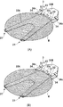
図2を参照してハンドユニット3について説明する。図2はハンドユニット3の斜視図である。ロボットアーム2の動作によりハンドユニット3の向きは多様に変化するが、説明の都合上、ここではハンドユニット3の長手方向(先端−手前方向)がX方向、幅方向がY方向を向いている状態にある時のハンドユニット3の構成を説明する。
<Hand unit>
The
ハンドユニット3は、ハンド部材30Aと、ベースユニット30Bとを備える。ハンド部材30Aは半導体ウェハが載置される板状の部材であり、その表面30c側が半導体ウェハが載置される載置部を形成する。なお、本実施形態の場合、ハンド部材30Aの表面30c上に直接半導体ウェハが載置されるわけではなく、後述する支持部材31〜33上に載置される。ハンド部材30Aは、表面30cがX−Y平面と平行な水平姿勢に維持されるが、上述した支持ユニット22によって表裏を反転することができる。
The
ハンド部材30Aは、フォーク状にX方向に延びる一対のフィンガ部fを備え、全体としてU字形をなしている。ハンド部材30Aの長手方向の一端部は、各フィンガ部fの先端部30aであり、他端部はフィンガ部f、fを束ねる根元部30bである。ハンド部材30Aは根元部30bにおいてベースユニット30Bに支持されている。
The
ハンド部材30Aの表面30c側には、半導体ウェハを支持する支持部材31〜33が設けられている。支持部材31〜33は、相対的に、支持部材31が先端部30a側に位置するように配置され、支持部材32および33が根元部30b側に位置するように配置される。本実施形態の場合、支持部材31は各先端部30aに一つずつ設けられている。支持部材31の数は、一つであってもよいし、三つ以上であってもよい。また、支持部材31の位置は、先端部30aの最先端の位置であってもよいし、最先端の位置から根元部30b側へ離れた位置であってもよい。
支持部材32は、Y方向に離間して二つ設けられている。支持部材32の数は、一つであってもよいし、三つ以上であってもよい。支持部材33は、Y方向に離間して二つ設けられている。支持部材33の数は、一つであってもよいし、三つ以上であってもよい。本実施形態の場合、Y方向で見ると、二つの支持部材33が、二つの支持部材32の間に位置している。しかし、支持部材32と支持部材33の配置はこれに限られるわけではない。例えば、二つの支持部材32が、二つの支持部材33の間に位置していてもよい。また、支持部材32と支持部材33とがY方向に交互に配置されていてもよい。
Two
本実施形態の場合、支持部材32はハンド部材30Aに固定され、支持部材33はハンド部材30A上を移動可能に配置される。しかし、支持部材32を移動可能に配置し、支持部材33を固定してもよい。あるいは、支持部材32と支持部材33の双方を移動可能に配置してもよい。本実施形態の場合、支持部材33はX方向に移動可能であり、支持部材31に対して進退動が可能である。X方向において、支持部材33が、支持部材31側へ移動することを前進あるいは進出とよび、支持部材31側から根本部30b側(ベースユニット30B側)へ移動することを後退あるいは退避と呼ぶ場合がある。
In the present embodiment, the
ベースユニット30Bは、ロボットアーム2に連結される部分である。ベースユニット30Bは駆動ユニット35および36を内蔵する。駆動ユニット35は支持部材33を支持部材31に対して進退動させるユニットである。本実施形態の場合、駆動ユニット35は駆動源35aと、伝達機構35bと、支持部材(被移動部材)35cとを備える。駆動源35aは例えばモータである。伝達機構35bは駆動源35aの駆動力を支持部材35cに伝達すると共に駆動力を支持部材35cの往復運動に変換する。伝達機構35bは例えばボールねじ機構やラック−ピニオン機構である。支持部材35cはT字形をなしており、その一方端部(基端部)が伝達機構35bに接続され、他方端部(先端部)における各分岐部に支持部材33がそれぞれ固定されている。
The base unit 30 </ b> B is a part connected to the
駆動ユニット36は保持部材34を支持部材31に対して進退動するユニットである。保持部材34は、根元部30b側に配置され、支持部材31と共に半導体ウェハを保持する部材である。本実施形態の場合、保持部材34はY方向に離間して二つ設けられている。保持部材34の数は、一つであってもよいし、三つ以上であってもよい。本実施形態の場合、Y方向で見ると、二つの保持部材34の間に、支持部材32および33が位置している。しかし、保持部材34の位置はこれに限られず、例えば、根元部30bのY方向中央部等に配置することも可能である。
The
本実施形態の場合、駆動ユニット36は駆動源36aと、伝達機構36bと、一対の支持部材36cとを備える。駆動源36aは例えばモータである。伝達機構36bは駆動源36aの駆動力を支持部材36cに伝達すると共に駆動力を支持部材36cの往復運動に変換する。伝達機構36bは例えばボールねじ機構やラック−ピニオン機構である。各支持部材36cはT字形をなしていると共に、分岐部の先端にそれぞれ突出部(アーム)を備えている。支持部材36cの一方端部(基端部)が伝達機構36bに接続され、突出部に保持部材34がそれぞれ固定されている。二つの保持部材34は同期的に移動される。したがって、一対の支持部材36cは一体の部材であってもよい。
In this embodiment, the
次に、半導体ウェハの支持態様および保持態様について説明する。本実施形態では、半導体ウェハの支持位置を変更可能とするため、半導体ウェハを支持する支持部材31〜33の組み合わせを切り替え可能となっている。半導体ウェハを支持する支持部材31〜33の組み合わせは、支持部材31と支持部材32の組と、支持部材31と支持部材33の組とがある。
Next, the support mode and holding mode of the semiconductor wafer will be described. In this embodiment, in order to change the support position of the semiconductor wafer, the combination of the
図3(A)および図3(B)は半導体ウェハWの支持態様の例を示している。半導体ウェハWは透視図として図示している。図3(A)は支持部材31と支持部材32の組で半導体ウェハWを支持した態様を示し、図3(B)は支持部材31と支持部材33の組で半導体ウェハWを支持した態様を示している。図3(A)と図3(B)では、支持部材33および保持部材34の位置が異なっている。図3(A)の例では支持部材33が図3(B)に対して相対的に、ベースユニット30B側に位置している。この位置を退避位置と呼ぶ場合がある。図3(B)の例では支持部材33が図3(A)に対して相対的に、支持部材31側に位置している。この位置を前進位置と呼ぶ場合がある。
FIG. 3A and FIG. 3B show examples of support modes of the semiconductor wafer W. The semiconductor wafer W is illustrated as a perspective view. 3A shows a mode in which the semiconductor wafer W is supported by a set of the
本実施形態では、支持部材33の位置変更により、半導体ウェハWの支持位置を変更することができる。支持部材33は、ハンドユニット3の構成部品の中で比較的小型の部品であり、その移動に大きな駆動力、すなわち出力の大きいアクチュエータを必要としない。
In the present embodiment, the support position of the semiconductor wafer W can be changed by changing the position of the
図3(A)の例では保持部材34が図3(B)に対して相対的に、ベースユニット30B側に位置している。この位置を後退位置と呼ぶ場合がある。保持部材34は、更にベースユニット30B側に位置可能である。この位置を退避位置と呼ぶ場合がある。図3(B)の例では保持部材34が図3(A)に対して相対的に、支持部材31側に位置している。この位置を前進位置と呼ぶ場合がある。
In the example of FIG. 3A, the holding
図3(A)に図示した支持部材31と支持部材32の組による支持態様について説明する。図4(A)は図2のI−I線断面図であり、図4(B)は図2のII−II線断面図である。なお、図2では保持部材34は前進位置に位置しているが、図4(B)は保持部材34が後退位置に位置している場合の断面図である。
A support mode by a set of the
支持部材31は、ハンド部材30Aの表面30cに対する半導体ウェハWの支持高さが異なる支持部31a、31bを備える。支持部31a、31bは別部材に形成されてもよいが、本実施形態の場合、一つの支持部材31に二つの支持部31a、31bが形成される。本実施形態の場合、支持部31aおよび支持部31bは、いずれも半導体ウェハWを下から支持する載置面であり、半導体ウェハWは支持部31aまたは支持部31b上に載置される。支持部31aおよび支持部31bは表面30cと平行であってもよいし、僅かに傾斜していてもよい。本実施形態の場合、支持部31aは根元部30b側に向かって僅かに下降した傾斜を有している。支持部31bも傾斜を有していてもよい。支持部31a、31bを傾斜させることでハンド部材30Aと半導体ウェハWとの接触面積をより小さくすることができる。
The
支持部31aは、表面30cから支持高さH1で半導体ウェハWを支持する面を形成し、支持部31aと支持部材32との組み合わせで半導体ウェハWが支持高さH1で支持される。支持部材32は、支持部32aを有している。支持部32aは全体として円錐形状を有しており、半導体ウェハWの下面を支持する載置面(円錐部の傾斜面)を備える。支持部32aは、表面30cと平行かあるいは僅かに傾斜している程度に形成してもよい。しかし、本実施形態における支持部32aのように、大きく傾斜した傾斜面に形成することで、半導体ウェハWを異なる支持高さで支持することに対応し易くなると共に、支持部材32と半導体ウェハWとの接触面積をより小さくすることができる。
The
支持部材31は、保持部材34との協働によって半導体ウェハWを保持(クランプ)する当接面31c、31dを備える。当接面31c、31dは別部材に形成されてもよく、更に、支持部31aや支持部31bと別部材に形成されてもよいが、本実施形態の場合、一つの支持部材31に二つの支持部31a、31bと二つの当接面31c、31dが設けられる。
The
保持部材34は、半導体ウェハWを保持する保持部34a、34bを備える。保持部34a、34bは本実施形態の場合、半導体ウェハWの端縁に当接する当接面を有する溝状に形成されている。半導体ウェハWは、当接面31cと保持部34aの組または当接面31dと保持部34bの組により、挟持されるようにして保持される。
The holding
当接面31cおよび保持部34aは、支持高さH1で半導体ウェハWを保持する。したがって、当接面31cと保持部34aとは表面30cに対して同じ高さに位置している。当接面31cは支持部31aの先端部30a側の端縁に連続し、かつ、支持部31aから上方へ立ち上がって形成されている。当接面31cは垂直面でもよいが、本実施形態の場合、垂直面から角度θだけ根元部30b側へ傾斜している。換言すると、当接面31cは支持部31aから根元部30b側へ向かって傾斜した上り傾斜面である。この構成により、支持部31aと当接面31cとが交差する部分は、その断面形状が楔形状の空間になる。当接面31cと保持部34aとで半導体ウェハWを挟持する際に、この楔形の空間に半導体ウェハWが嵌り込むため、これによって、半導体ウェハWの保持力が向上する。
The
次に、図3(B)に図示した支持部材31と支持部材33の組による支持態様について説明する。図4(C)は図2のIII−III線断面図であり、支持部材33は前進位置に位置している。図4(D)は図2のII−II線断面図に相当し、保持部材34が前進位置に位置している場合を示している。
Next, a description will be given of a support mode by a set of the
支持部31bは、表面30cから支持高さH2で半導体ウェハWを支持する面を形成し、支持部31bと支持部材33との組み合わせで半導体ウェハWが支持高さH2で支持される。支持高さH2は支持高さH1よりも高い。支持部31bは、支持部31aよりも先端部30a側に位置している。したがって、半導体ウェハWの支持位置は図3(A)の支持態様と図3(B)の支持態様では、高さだけでなく水平位置も異なっている。図3(B)の支持態様の場合、図3(A)の支持態様に比べて、半導体ウェハWの支持位置が先端部30a側にオフセットされている。
The
支持部材33は、支持部33aを有している。本実施形態の場合、支持部材32と支持部材33とは同じ部品であり、支持部33aは支持部32aと同様に半導体ウェハWの下面を支持する載置面(円錐部の傾斜面)を備える。支持部材32と支持部材33とは異なる部品であってもよいが、同じ部品とすることで部品種を削減することができる。
The
当接面31dおよび保持部34bは、支持高さH2で半導体ウェハWを保持する。したがって、当接面31dと保持部34bとは表面30cに対して同じ高さに位置している。当接面31dは支持部31bの先端部30a側の端縁に連続し、かつ、支持部31bから上方へ立ち上がって形成されている。当接面31dは垂直面でもよいが、本実施形態の場合、当接面31cと同様、垂直面から根元部30b側へ傾斜している。換言すると、当接面31dは支持部31bから根元部30b側へ向かって傾斜した上り傾斜面である。この構成により、支持部31bと当接面31dとが交差する部分は、その断面形状がが楔形状の空間になる。当接面31dと保持部34bとで半導体ウェハWを挟持する際に、この楔形の空間に半導体ウェハWが嵌り込むため、これによって、半導体ウェハWの保持力が向上する。
The
<移載例>
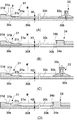
搬送装置1による半導体ウェハWの移載例について図5〜図8を参照して説明する。ここでは、不図示のカセットから半導体ウェハWを取り出し、不図示の洗浄装置に搬送した後、この洗浄装置から不図示の別のカセットへ半導体ウェハWを搬送する際のハンドユニット3の動作を説明する。既に述べたとおり、搬送処理の間、ハンドユニット3の向きは多様に変化するが、説明の都合上、ハンドユニット3の長手方向(先端−手前方向)がX方向、幅方向がY方向を向いている状態にある時のハンドユニット3の動作を説明する。
<Transfer example>
An example of transferring the semiconductor wafer W by the
図5の状態ST1〜図6の状態ST6はカセットから半導体ウェハWを取り出し、洗浄装置に搬送する工程を示している。本実施形態の場合、洗浄処理前は半導体ウェハWを支持高さH1で支持し、洗浄処理後は支持高さH2で支持する。この関係は逆でもよいが、洗浄処理後に、より高い位置である支持高さH2で支持した方が、洗浄処理前に半導体ウェハWからハンドユニット3に付着した汚れ等が洗浄処理後の半導体ウェハWに付着しにくいため、より好ましい。
State ST1 in FIG. 5 to state ST6 in FIG. 6 show a process of taking out the semiconductor wafer W from the cassette and transporting it to the cleaning device. In the present embodiment, the semiconductor wafer W is supported at the support height H1 before the cleaning process, and is supported at the support height H2 after the cleaning process. This relationship may be reversed, but if the support height H2 is higher after the cleaning process, dirt attached to the
まず、ハンドユニット3が半導体ウェハWを取り出す水平位置および高さに移動される。状態ST1では、支持部材32の支持部32aと支持部材33の支持部33aの相対的な配置を変更する配置変更処理を行う。上記のとおり、洗浄処理前は半導体ウェハWを支持高さH1で支持されることから、支持部材31と支持部材32とが半導体ウェハWを支持する。このため、駆動ユニット35を駆動し、状態ST1において矢印で示すように支持部材33が退避位置に移動される。また、保持部材34は退避位置に位置している。
First, the
状態ST2ではハンド部材30Aが半導体ウェハWの下に位置するように搬送装置1によりハンドユニット3を移動する。このとき、支持部31aと半導体ウェハWの周縁部とが上下に重なる位置にハンドユニット3が移動される。続いて搬送装置1によりハンドユニット3を上昇させ、半導体ウェハWがカセットの載置部から掬い上げられ、半導体ウェハWがカセットからハンドユニット3に移載される。このとき、半導体ウェハWは支持部31aおよび支持部32a上に、支持高さH1、水平姿勢で載置される。
In the state ST2, the
状態ST3では駆動ユニット36が駆動され、保持部材34が後退位置に移動される。これにより、支持部31a上の半導体ウェハWが当接部31cに向けて水平移動され、最終的には当接部31cと保持部材34の保持部34aとの間に挟まれるようにして保持され、半導体ウェハWの高速搬送や、反転動作(ハンドユニット3の表裏反転による半導体ウェハWの表裏反転)が可能となる。
In the state ST3, the
続いて搬送装置1により半導体ウェハWが洗浄装置へ向けて搬送される。状態ST4は洗浄装置の載置部上方に半導体ウェハWが搬送された状態を示す。状態ST5では駆動ユニット36が駆動され、保持部材34が退避位置に移動される。これにより、半導体ウェハWの保持が解除される。続いて搬送装置1によりハンドユニット3が下降され、半導体ウェハWがハンドユニット3から洗浄装置に移載され、洗浄装置の載置部上に半導体ウェハWが載置される。その後、状態ST6に示すように、搬送装置1により矢印方向にハンドユニット3が移動され、洗浄装置からハンドユニット3が退避される。以上により、カセットから洗浄装置への半導体ウェハWの搬送が完了する。
Subsequently, the semiconductor device W is transported toward the cleaning device by the
半導体ウェハWの洗浄が終わると、今度は、洗浄装置からカセットへ半導体ウェハWが搬送される。図7の状態ST7〜図8の状態ST12は洗浄装置から半導体ウェハWを取り出し、カセットに搬送する工程を示している。 When the cleaning of the semiconductor wafer W is completed, the semiconductor wafer W is now transferred from the cleaning device to the cassette. State ST7 in FIG. 7 to state ST12 in FIG. 8 show a process of taking out the semiconductor wafer W from the cleaning apparatus and transporting it to the cassette.
まず、ハンドユニット3が半導体ウェハWを取り出す水平位置および高さに移動される。状態ST7では、支持部材32の支持部32aと支持部材33の支持部33aの相対的な配置を変更する配置変更処理を行う。上記のとおり、洗浄処理後は半導体ウェハWを支持高さH2で支持されることから支持部材31と支持部材33とが半導体ウェハWを支持する。このため、駆動ユニット35を駆動し、状態ST7において矢印で示すように支持部材33が前進位置に移動される。また、保持部材34は退避位置に位置している。
First, the
状態ST8ではハンド部材30Aが半導体ウェハWの下に位置するように搬送装置1によりハンドユニット3が移動される。このとき、支持部31bと半導体ウェハWの周縁部とが上下に重なる位置にハンドユニット3が移動される。続いて搬送装置1によりハンドユニット3を上昇させ、半導体ウェハWが洗浄装置の載置部から掬い上げられ、半導体ウェハWが洗浄装置からハンドユニット3に移載される。このとき、半導体ウェハWは支持部31bおよび支持部33a上に、支持高さH2、水平姿勢で載置される。
In the state ST8, the
状態ST9では駆動ユニット36が駆動され、保持部材34が前進位置に移動される。これにより、支持部31b上の半導体ウェハWが当接部31dに向けて水平移動され、最終的には当接部31dと保持部材34の保持部34bとの間に挟まれるようにして保持され、半導体ウェハWの高速搬送や、反転動作が可能となる。
In the state ST9, the
続いて搬送装置1により半導体ウェハWがカセットへ向けて搬送される。状態ST10はカセットの載置部上方に半導体ウェハWが搬送された状態を示す。状態ST11では駆動ユニット36を駆動させ、保持部材34が退避位置に移動される。これにより、半導体ウェハWの保持が解除される。続いて搬送装置1によりハンドユニット3が下降され、半導体ウェハWがハンドユニット3からカセットに移載され、カセットの載置部上に半導体ウェハWが載置される。その後、状態ST12に示すように、搬送装置1により矢印方向にハンドユニット3が移動され、カセットからハンドユニット3が退避される。その後、状態ST6に示すように、搬送装置1により矢印方向にハンドユニット3が移動され、洗浄装置からハンドユニット3が退避される。以上により、洗浄装置からカセットへの半導体ウェハWの搬送が完了する。以降、同様の手順を繰り返すことで処理が進行していくことになる。
Subsequently, the semiconductor wafer W is transferred toward the cassette by the
以上より、本実施形態に係るハンドユニット3によれば、一組のハンドユニット3を用いながら、例えば、洗浄処理前と洗浄処理後において、半導体ウェハWの支持位置を変えることができる。これにより、洗浄処理前に半導体ウェハWからハンドユニット3に付着していた汚れ等があったとしても、洗浄処理後の半導体ウェハWをハンドユニット3に再度移載した際に、その汚れが半導体ウェハWに付着することはない。
As described above, according to the
また、本実施形態に係るハンドユニット3は、半導体ウェハWを水平姿勢で移載することから、移載の際に、半導体ウェハWの傾きに由来するパーティクルが発生することはない。
In addition, since the
一方、半導体製造工程では、搬送装置1による半導体ウェハWの搬送途中において、ハンドユニット3を水平軸周りに回転させ、ハンドユニット3上の半導体ウェハWを表裏反転させる場合がある。このとき、半導体ウェハの外縁を接触支持するだけのハンドユニットでは、ハンドユニットを回転させたときに半導体ウェハが落下してしまう。
On the other hand, in the semiconductor manufacturing process, during the transfer of the semiconductor wafer W by the
しかしながら、本実施形態に係るハンドユニット3は、半導体ウェハWを当接面31cと保持部34a(又は当接面31dと保持部34b)とで半導体ウェハWを挟持する際、半導体ウェハWにおける当接面31c(又は当接面31d)側の上面端縁は楔形の空間部に嵌りこんでいる。そして、半導体ウェハWにおける当接面31c(又は当接面31d)側の上面端縁は、この空間部によりハンド部材30Aの表面30c側に向けて付勢された状態にある。よって、半導体ウェハWはこのような状態でハンドユニット3により挟持されていることから、ハンドユニット3を表裏反転させても、半導体ウェハWがハンドユニット3から落下するおそれはない。
However, in the
3:ハンドユニット 31〜33:支持部材 31a、31b、32a、33a:支持部 34:保持部材 34a、34b:保持部 35、36:駆動ユニット
3: Hand unit 31-33:
Claims (13)
前記載置部の一端側に、前記半導体ウェハを第一の支持高さで支持する第一の支持部及び第二の支持高さで支持する第二の支持部を備え、
前記載置部の他端側に、前記半導体ウェハを前記第一の支持高さで支持する第三の支持部及び前記第二の支持高さで支持する第四の支持部を備え
前記ハンドユニットは、更に、前記第三の支持部及び前記第四の支持部の少なくとも一方を、前記第一の支持部および前記第二の支持部に対して進退動させる第一の駆動ユニットを備える、
ことを特徴とするハンドユニット。 A robot arm hand unit having a U-shaped mounting portion on which a semiconductor wafer is mounted,
Provided on one end side of the mounting portion with a first support portion for supporting the semiconductor wafer at a first support height and a second support portion for supporting at a second support height;
The hand unit includes a third support part for supporting the semiconductor wafer at the first support height and a fourth support part for supporting the semiconductor wafer at the second support height on the other end side of the placement part. Further includes a first drive unit for moving at least one of the third support part and the fourth support part forward and backward with respect to the first support part and the second support part.
A hand unit characterized by that.
前記第一の支持部および前記第二の支持部はそれぞれ、前記半導体ウェハの下面を支持する載置面と、前記半導体ウェハの端縁に当接する当接面とを備え、
前記第三の支持部および前記第四の支持部はそれぞれ、半導体ウェハの下面を支持する傾斜した載置面を備える、
ことを特徴とするハンドユニット。 The hand unit according to claim 1,
Each of the first support portion and the second support portion includes a mounting surface that supports a lower surface of the semiconductor wafer, and a contact surface that contacts an edge of the semiconductor wafer,
The third support portion and the fourth support portion each include an inclined mounting surface that supports the lower surface of the semiconductor wafer.
A hand unit characterized by that.
前記他端側に、前記半導体ウェハを前記第一の支持高さで保持する第一の保持部と、前記第二の支持高さで保持する第二の保持部とを更に備える、
ことを特徴とするハンドユニット。 The hand unit according to claim 2,
The other end side further includes a first holding unit that holds the semiconductor wafer at the first support height, and a second holding unit that holds the semiconductor wafer at the second support height.
A hand unit characterized by that.
前記第一の保持部および前記第二の保持部を、前記第一の支持部および前記第二の支持部に対して進退動させる第二の駆動ユニットを更に備える、
ことを特徴とするハンドユニット。 The hand unit according to claim 3,
A second drive unit that moves the first holding portion and the second holding portion forward and backward with respect to the first support portion and the second support portion;
A hand unit characterized by that.
前記当接面は、前記載置面の前記一端側と連続し、かつ、前記他端側へ向かって上方へ傾斜した傾斜面である、
ことを特徴とするハンドユニット。 The hand unit according to claim 2,
The contact surface is an inclined surface that is continuous with the one end side of the mounting surface and is inclined upward toward the other end side.
A hand unit characterized by that.
前記ハンドユニットは、
板状のU字形ハンド部材と、
前記ハンド部材の先端側に設けられた第一の支持部材と、
前記ハンド部材の根本側に設けられた第二の支持部材と、
前記ハンド部材の前記根本側に設けられた第三の支持部材と、
第一の駆動ユニットと、を備え、
前記第一の支持部材は、半導体ウェハを前記ハンド部材の表面から第一の支持高さで支持する第一の支持部及び前記表面から第二の支持高さで支持する第二の支持部を備え、
前記第二の支持部材は、半導体ウェハを前記表面から前記第一の支持高さで支持する第三の支持部を備え、
前記第三の支持部材は、前記表面から前記第二の支持高さで支持する第四の支持部を備え、
前記第一の駆動ユニットは、前記第二の支持部材または前記第三の支持部材の少なくとも一方を前記第一の支持部材に対して進退動させる、
ことを特徴とするハンドユニット。 A robot arm hand unit for transferring a semiconductor wafer,
The hand unit is
A plate-shaped U-shaped hand member;
A first support member provided on the distal end side of the hand member;
A second support member provided on the base side of the hand member;
A third support member provided on the base side of the hand member;
A first drive unit,
The first support member includes a first support portion that supports the semiconductor wafer at a first support height from the surface of the hand member, and a second support portion that supports the semiconductor wafer at a second support height from the surface. Prepared,
The second support member includes a third support portion that supports the semiconductor wafer from the surface at the first support height,
The third support member includes a fourth support portion that supports the second support height from the surface,
The first drive unit moves the at least one of the second support member or the third support member forward and backward with respect to the first support member.
A hand unit characterized by that.
前記根本側に設けられた保持部材を更に備え、
前記保持部材は、前記半導体ウェハを前記表面から前記第一の支持高さで保持する第一の保持部及び前記表面から前記前記第二の支持高さで保持する第二の保持部を備える、
ことを特徴とするハンドユニット。 The hand unit according to claim 6,
A holding member provided on the root side;
The holding member includes a first holding unit that holds the semiconductor wafer from the surface at the first support height, and a second holding unit that holds the semiconductor wafer at the second support height from the surface.
A hand unit characterized by that.
前記保持部材を、前記第一の支持部材に対して進退動させる第二の駆動ユニットを更に備える
ことを特徴とするハンドユニット。 The hand unit according to claim 7,
A hand unit, further comprising a second drive unit for moving the holding member forward and backward relative to the first support member.
前記ハンドユニットが、
前記載置部の一端側に配置された、前記半導体ウェハを第一の支持高さで支持する第一の支持部及び第二の支持高さで支持する第二の支持部と、
前記載置部の他端側に配置された、前記半導体ウェハを支持する第三の支持部及び第四の支持部と、を備え、
前記移載方法は、
処理前の半導体ウェハを移載する第一の移載工程と、
処理後の半導体ウェハを移載する第二の移載工程と、を含み、
前記第一の移載工程は、
前記第三の支持部及び前記第四の支持部のうちの一方を移動する第一の移動工程と、
前記半導体ウェハを、前記第一の支持部と、前記第三の支持部及び前記第四の支持部のうちの他方とで、前記第一の支持高さで支持する第一の支持工程と、を含み、
前記第二の移載工程は、
前記第三の支持部及び前記第四の支持部のうちの前記一方を移動する第二の移動工程と、
前記半導体ウェハを、前記第二の支持部と、前記第三の支持部及び前記第四の支持部のうちの前記一方とで、前記第二の支持高さで支持する第二の支持工程と、を含む、
ことを特徴とする移載方法。 A transfer method of transferring a semiconductor wafer by a hand unit of a robot arm having a U-shaped mounting portion on which a semiconductor wafer is mounted,
The hand unit is
A first support portion disposed on one end side of the mounting portion and supporting the semiconductor wafer at a first support height and a second support portion supporting the semiconductor wafer at a second support height;
A third support part and a fourth support part, which are arranged on the other end side of the placement part and support the semiconductor wafer,
The transfer method is:
A first transfer step of transferring a semiconductor wafer before processing;
A second transfer step of transferring the processed semiconductor wafer,
The first transfer process includes
A first moving step of moving one of the third support portion and the fourth support portion;
A first support step of supporting the semiconductor wafer at the first support height with the first support portion and the other of the third support portion and the fourth support portion; Including
The second transfer step includes
A second moving step of moving the one of the third support portion and the fourth support portion;
A second support step of supporting the semiconductor wafer at the second support height with the second support portion and the one of the third support portion and the fourth support portion; ,including,
A transfer method characterized by that.
前記ハンドユニットが、
前記載置部の一端側に配置された、前記半導体ウェハを第一の支持高さで支持する第一の支持部及び第二の支持高さで支持する第二の支持部と、
前記載置部の他端側に配置された、前記半導体ウェハを支持する第三の支持部及び第四の支持部と、を備え、
前記移載方法は、
処理前の半導体ウェハを移載する第一の移載工程と、
処理後の半導体ウェハを移載する第二の移載工程と、を含み、
前記第一の移載工程は、
前記第三の支持部及び前記第四の支持部の相対的な配置を変更する第一の配置変更工程と、
前記半導体ウェハを、前記第一の支持部と、前記第三の支持部とで、前記第一の支持高さで支持する第一の支持工程と、を含み、
前記第二の移載工程は、
前記第三の支持部及び前記第四の支持部の相対的な配置を変更する第二の配置変更工程と、
前記半導体ウェハを、前記第二の支持部と、前記第四の支持部とで、前記第二の支持高さで支持する第二の支持工程を含む、
ことを特徴とする移載方法。 A transfer method of transferring a semiconductor wafer by a hand unit of a robot arm having a U-shaped mounting portion on which a semiconductor wafer is mounted,
The hand unit is
A first support portion disposed on one end side of the mounting portion and supporting the semiconductor wafer at a first support height and a second support portion supporting the semiconductor wafer at a second support height;
A third support part and a fourth support part, which are arranged on the other end side of the placement part and support the semiconductor wafer,
The transfer method is:
A first transfer step of transferring a semiconductor wafer before processing;
A second transfer step of transferring the processed semiconductor wafer,
The first transfer process includes
A first arrangement changing step of changing a relative arrangement of the third support part and the fourth support part;
A first support step of supporting the semiconductor wafer at the first support height with the first support portion and the third support portion,
The second transfer step includes
A second arrangement changing step of changing a relative arrangement of the third support part and the fourth support part;
Including a second support step of supporting the semiconductor wafer at the second support height with the second support portion and the fourth support portion;
A transfer method characterized by that.
前記第一の移載工程では、処理前の前記半導体ウェハが前記載置部上の第一の水平位置で支持され、
前記第二の移載工程では、処理後の前記半導体ウェハが前記第一の水平位置に対して前記一端側にオフセットされた、前記載置部上の第二の水平位置で支持され、
前記第一の移動工程では、前記第三の支持部及び前記第四の支持部のうちの前記他方が、前記第一の水平位置に対応した位置に位置し、
前記第二の移動工程では、前記第三の支持部及び前記第四の支持部のうちの前記一方が、前記第二の水平位置に対応した位置に位置する、
ことを特徴とする移載方法。 The transfer method according to claim 9 or 10, wherein
In the first transfer step, the semiconductor wafer before processing is supported at a first horizontal position on the placement unit,
In the second transfer step, the processed semiconductor wafer is supported at the second horizontal position on the mounting portion, which is offset to the one end side with respect to the first horizontal position,
In the first moving step, the other of the third support part and the fourth support part is located at a position corresponding to the first horizontal position,
In the second moving step, the one of the third support part and the fourth support part is located at a position corresponding to the second horizontal position.
A transfer method characterized by that.
前記第二の支持高さは、前記第一の支持高さに対して鉛直方向上側にオフセットされた高さである、
ことを特徴とする移載方法。 The transfer method according to claim 11,
The second support height is a height that is offset upward in the vertical direction with respect to the first support height.
A transfer method characterized by that.
前記ハンドユニットは、更に、
前記載置部の前記他端側に配置され、前記半導体ウェハを前記第一の支持高さで保持する第一の保持部と、
前記載置部の前記他端側に配置され、前記半導体ウェハを前記第二の支持高さで保持する第二の保持部と、を備え、
前記第一の移載工程は、
前記第一の保持部を前記第一の支持部に向かって進出させ、前記第一の支持部と前記第三の支持部または前記第四の支持部の一方とで前記第一の支持高さに支持された半導体ウェハを、前記第一の支持部と前記第一の保持部とで挟持する第一の挟持工程を含み、
前記第二の移載工程は、
前記第二の保持部を前記第二の支持部に向かって進出させ、前記第二の支持部と前記第三の支持部または前記第四の支持部の他方とで前記第二の支持高さに支持された半導体ウェハを、前記第二の支持部と前記第二の保持部とで挟持する第二の挟持工程を含む、
ことを特徴とする移載方法。 A transfer method according to claim 9 or claim 10, wherein
The hand unit further comprises:
A first holding part that is disposed on the other end side of the mounting part and holds the semiconductor wafer at the first support height;
A second holding part that is disposed on the other end side of the mounting part and holds the semiconductor wafer at the second support height;
The first transfer process includes
The first support portion is advanced toward the first support portion, and the first support height and the first support height are one of the third support portion and the fourth support portion. Including a first clamping step of clamping the semiconductor wafer supported by the first supporting part and the first holding part,
The second transfer step includes
The second holding portion is advanced toward the second supporting portion, and the second supporting height is set between the second supporting portion and the other of the third supporting portion and the fourth supporting portion. Including a second clamping step of clamping the semiconductor wafer supported by the second supporting part and the second holding part,
A transfer method characterized by that.
Priority Applications (5)
| Application Number | Priority Date | Filing Date | Title |
|---|---|---|---|
| JP2016071015A JP6276317B2 (en) | 2016-03-31 | 2016-03-31 | Hand unit and transfer method |
| TW106107406A TWI654714B (en) | 2016-03-31 | 2017-03-07 | Robot unit and transfer method |
| KR1020170039079A KR101940199B1 (en) | 2016-03-31 | 2017-03-28 | Hand unit and transfer method |
| US15/473,064 US10109515B2 (en) | 2016-03-31 | 2017-03-29 | Hand unit and transfer method |
| CN201710199756.7A CN107275268B (en) | 2016-03-31 | 2017-03-30 | Robot unit and transfer method |
Applications Claiming Priority (1)
| Application Number | Priority Date | Filing Date | Title |
|---|---|---|---|
| JP2016071015A JP6276317B2 (en) | 2016-03-31 | 2016-03-31 | Hand unit and transfer method |
Publications (2)
| Publication Number | Publication Date |
|---|---|
| JP2017183593A true JP2017183593A (en) | 2017-10-05 |
| JP6276317B2 JP6276317B2 (en) | 2018-02-07 |
Family
ID=59961188
Family Applications (1)
| Application Number | Title | Priority Date | Filing Date |
|---|---|---|---|
| JP2016071015A Active JP6276317B2 (en) | 2016-03-31 | 2016-03-31 | Hand unit and transfer method |
Country Status (5)
| Country | Link |
|---|---|
| US (1) | US10109515B2 (en) |
| JP (1) | JP6276317B2 (en) |
| KR (1) | KR101940199B1 (en) |
| CN (1) | CN107275268B (en) |
| TW (1) | TWI654714B (en) |
Cited By (1)
| Publication number | Priority date | Publication date | Assignee | Title |
|---|---|---|---|---|
| JP7420954B2 (en) | 2020-09-03 | 2024-01-23 | 川崎重工業株式会社 | Substrate holding hand and substrate transfer robot |
Families Citing this family (11)
| Publication number | Priority date | Publication date | Assignee | Title |
|---|---|---|---|---|
| KR102429490B1 (en) | 2017-09-05 | 2022-08-05 | 현대자동차주식회사 | Svm system for providing bvm image and operation method of the same |
| USD911986S1 (en) * | 2019-05-03 | 2021-03-02 | Raytheon Company | Handheld semiconductor wafer handling tool |
| KR20210155813A (en) * | 2019-05-14 | 2021-12-23 | 매슨 테크놀로지 인크 | Plasma Processing Apparatus With Focus Ring Adjustment Assembly |
| CN110039530A (en) * | 2019-05-28 | 2019-07-23 | 北京半导体专用设备研究所(中国电子科技集团公司第四十五研究所) | Manipulator |
| JP1665227S (en) * | 2019-11-28 | 2020-08-03 | ||
| JP7415782B2 (en) * | 2020-05-11 | 2024-01-17 | 東京エレクトロン株式会社 | Substrate transfer mechanism and substrate transfer method |
| JP2022011045A (en) * | 2020-06-29 | 2022-01-17 | キヤノン株式会社 | Conveyance apparatus, substrate processing apparatus, and article manufacturing method |
| KR20230061535A (en) * | 2020-09-08 | 2023-05-08 | 어플라이드 머티어리얼스, 인코포레이티드 | Methods and Substrate Handling Systems for CMP Processing |
| US11926039B2 (en) * | 2020-12-25 | 2024-03-12 | Kawasaki Jukogyo Kabushiki Kaisha | Robot |
| CN113113340A (en) * | 2021-03-30 | 2021-07-13 | 北京北方华创微电子装备有限公司 | Manipulator of semiconductor equipment |
| CN117373994A (en) * | 2023-11-17 | 2024-01-09 | 上海普达特半导体设备有限公司 | Robot for transporting wafers and semiconductor processing apparatus |
Citations (6)
| Publication number | Priority date | Publication date | Assignee | Title |
|---|---|---|---|---|
| JPH0687531A (en) * | 1992-09-09 | 1994-03-29 | Hitachi Ltd | Delivery jig and device |
| JPH06349933A (en) * | 1993-06-10 | 1994-12-22 | Sony Corp | Wafer transfer apparatus |
| JPH1131732A (en) * | 1997-05-15 | 1999-02-02 | Tokyo Electron Ltd | Substrate-carrying device and its method |
| JP2011119347A (en) * | 2009-12-01 | 2011-06-16 | Kawasaki Heavy Ind Ltd | Edge grip device, transfer robot with the same, and method of releasing wafer for semiconductor process |
| JP2013042175A (en) * | 2012-11-13 | 2013-02-28 | Tokyo Electron Ltd | Substrate holding member, substrate transfer arm, and substrate transfer apparatus |
| JP2014086472A (en) * | 2012-10-19 | 2014-05-12 | Sinfonia Technology Co Ltd | Clamp device and workpiece conveyer robot |
Family Cites Families (16)
| Publication number | Priority date | Publication date | Assignee | Title |
|---|---|---|---|---|
| JPS563857B2 (en) | 1972-12-06 | 1981-01-27 | ||
| JPS5490860A (en) | 1977-12-27 | 1979-07-18 | Toyobo Co Ltd | Waste water treating apparatus |
| US4290263A (en) | 1979-12-12 | 1981-09-22 | General Motors Corporation | Diesel engine exhaust trap particulate distribution and incineration balancing system |
| TW401582B (en) | 1997-05-15 | 2000-08-11 | Tokyo Electorn Limtied | Apparatus for and method of transferring substrates |
| KR100331157B1 (en) * | 1998-07-24 | 2002-04-03 | 다니구찌 이찌로오, 기타오카 다카시 | Wafer holding hand |
| US7641247B2 (en) * | 2002-12-17 | 2010-01-05 | Applied Materials, Inc. | End effector assembly for supporting a substrate |
| JP4976811B2 (en) * | 2006-10-30 | 2012-07-18 | 東京エレクトロン株式会社 | Substrate processing system, substrate transfer apparatus, substrate transfer method, and recording medium |
| US8141926B2 (en) * | 2008-02-06 | 2012-03-27 | Ulvac, Inc. | Robot hand for substrate transfer |
| JP2010258170A (en) * | 2009-04-23 | 2010-11-11 | Tokyo Electron Ltd | Substrate holding member, substrate transfer arm, and substrate carrier |
| JP5491834B2 (en) * | 2009-12-01 | 2014-05-14 | 川崎重工業株式会社 | Edge grip device and robot including the same. |
| JP5589790B2 (en) * | 2010-03-31 | 2014-09-17 | 株式会社安川電機 | Substrate transfer hand and substrate transfer robot |
| JP5698518B2 (en) * | 2010-12-21 | 2015-04-08 | 川崎重工業株式会社 | End effector for transfer robot |
| JP5549655B2 (en) * | 2011-09-26 | 2014-07-16 | 株式会社安川電機 | Hand and robot |
| JP5490860B2 (en) * | 2012-09-18 | 2014-05-14 | 大日本スクリーン製造株式会社 | Substrate transport apparatus and substrate processing apparatus having the same |
| JP6335587B2 (en) * | 2014-03-31 | 2018-05-30 | 株式会社荏原製作所 | Substrate holding mechanism, substrate transfer device, semiconductor manufacturing device |
| US9425076B2 (en) * | 2014-07-03 | 2016-08-23 | Applied Materials, Inc. | Substrate transfer robot end effector |
-
2016
- 2016-03-31 JP JP2016071015A patent/JP6276317B2/en active Active
-
2017
- 2017-03-07 TW TW106107406A patent/TWI654714B/en active
- 2017-03-28 KR KR1020170039079A patent/KR101940199B1/en active IP Right Grant
- 2017-03-29 US US15/473,064 patent/US10109515B2/en active Active
- 2017-03-30 CN CN201710199756.7A patent/CN107275268B/en active Active
Patent Citations (6)
| Publication number | Priority date | Publication date | Assignee | Title |
|---|---|---|---|---|
| JPH0687531A (en) * | 1992-09-09 | 1994-03-29 | Hitachi Ltd | Delivery jig and device |
| JPH06349933A (en) * | 1993-06-10 | 1994-12-22 | Sony Corp | Wafer transfer apparatus |
| JPH1131732A (en) * | 1997-05-15 | 1999-02-02 | Tokyo Electron Ltd | Substrate-carrying device and its method |
| JP2011119347A (en) * | 2009-12-01 | 2011-06-16 | Kawasaki Heavy Ind Ltd | Edge grip device, transfer robot with the same, and method of releasing wafer for semiconductor process |
| JP2014086472A (en) * | 2012-10-19 | 2014-05-12 | Sinfonia Technology Co Ltd | Clamp device and workpiece conveyer robot |
| JP2013042175A (en) * | 2012-11-13 | 2013-02-28 | Tokyo Electron Ltd | Substrate holding member, substrate transfer arm, and substrate transfer apparatus |
Cited By (1)
| Publication number | Priority date | Publication date | Assignee | Title |
|---|---|---|---|---|
| JP7420954B2 (en) | 2020-09-03 | 2024-01-23 | 川崎重工業株式会社 | Substrate holding hand and substrate transfer robot |
Also Published As
| Publication number | Publication date |
|---|---|
| CN107275268B (en) | 2020-09-15 |
| US10109515B2 (en) | 2018-10-23 |
| TW201737410A (en) | 2017-10-16 |
| JP6276317B2 (en) | 2018-02-07 |
| TWI654714B (en) | 2019-03-21 |
| KR101940199B1 (en) | 2019-01-18 |
| CN107275268A (en) | 2017-10-20 |
| KR20170113314A (en) | 2017-10-12 |
| US20170287759A1 (en) | 2017-10-05 |
Similar Documents
| Publication | Publication Date | Title |
|---|---|---|
| JP6276317B2 (en) | Hand unit and transfer method | |
| JP4726776B2 (en) | Inversion apparatus and substrate processing apparatus having the same | |
| JP4744426B2 (en) | Substrate processing apparatus and substrate processing method | |
| JP5004612B2 (en) | Substrate processing equipment | |
| JP4744425B2 (en) | Substrate processing equipment | |
| JP4852719B2 (en) | Articulated robot | |
| WO2006109791A1 (en) | Multi-joint robot | |
| US9343344B2 (en) | End effector device | |
| JP2006289555A (en) | Articulated robot | |
| WO2016166952A1 (en) | Substrate conveying robot and end effector for same | |
| JP5169557B2 (en) | Substrate lifting / lowering transfer apparatus and substrate processing / transfer system | |
| JP5283930B2 (en) | Transport device | |
| TWI656003B (en) | Substrate transfer system and method | |
| JP2015196241A (en) | Conveyance robot equipped with eight robot arm | |
| JP3974985B2 (en) | Substrate transfer device | |
| JPH10209241A (en) | Substrate transfer device and substrate treatment device provided with it | |
| KR20090099203A (en) | Lead soldering systemof semiconductor package | |
| JP4869097B2 (en) | Substrate processing equipment | |
| KR20140061279A (en) | Hand for conveying substrate and method for conveying substrate | |
| JP3615042B2 (en) | Substrate transfer device | |
| TWI750741B (en) | Industrial robot | |
| KR200431683Y1 (en) | Apparatus for moving wafer | |
| KR20090032651A (en) | Apparatus for transfering substrate | |
| JP2010186898A (en) | Bonding equipment |
Legal Events
| Date | Code | Title | Description |
|---|---|---|---|
| A131 | Notification of reasons for refusal |
Free format text: JAPANESE INTERMEDIATE CODE: A131 Effective date: 20171006 |
|
| A521 | Request for written amendment filed |
Free format text: JAPANESE INTERMEDIATE CODE: A523 Effective date: 20171031 |
|
| TRDD | Decision of grant or rejection written | ||
| A01 | Written decision to grant a patent or to grant a registration (utility model) |
Free format text: JAPANESE INTERMEDIATE CODE: A01 Effective date: 20171222 |
|
| A61 | First payment of annual fees (during grant procedure) |
Free format text: JAPANESE INTERMEDIATE CODE: A61 Effective date: 20180111 |
|
| R150 | Certificate of patent or registration of utility model |
Ref document number: 6276317 Country of ref document: JP Free format text: JAPANESE INTERMEDIATE CODE: R150 |
|
| R250 | Receipt of annual fees |
Free format text: JAPANESE INTERMEDIATE CODE: R250 |
|
| R250 | Receipt of annual fees |
Free format text: JAPANESE INTERMEDIATE CODE: R250 |