JP2017163082A - High electron mobility transistor, and manufacturing method of high electron mobility transistor - Google Patents
High electron mobility transistor, and manufacturing method of high electron mobility transistor Download PDFInfo
- Publication number
- JP2017163082A JP2017163082A JP2016048292A JP2016048292A JP2017163082A JP 2017163082 A JP2017163082 A JP 2017163082A JP 2016048292 A JP2016048292 A JP 2016048292A JP 2016048292 A JP2016048292 A JP 2016048292A JP 2017163082 A JP2017163082 A JP 2017163082A
- Authority
- JP
- Japan
- Prior art keywords
- layer
- concentration
- type semiconductor
- barrier layer
- mobility transistor
- Prior art date
- Legal status (The legal status is an assumption and is not a legal conclusion. Google has not performed a legal analysis and makes no representation as to the accuracy of the status listed.)
- Granted
Links
- 238000004519 manufacturing process Methods 0.000 title claims description 15
- 239000004065 semiconductor Substances 0.000 claims abstract description 94
- 230000004888 barrier function Effects 0.000 claims abstract description 76
- 239000000758 substrate Substances 0.000 claims description 33
- 238000005530 etching Methods 0.000 claims description 13
- QTBSBXVTEAMEQO-UHFFFAOYSA-N Acetic acid Chemical compound CC(O)=O QTBSBXVTEAMEQO-UHFFFAOYSA-N 0.000 claims description 9
- KRKNYBCHXYNGOX-UHFFFAOYSA-N citric acid Chemical compound OC(=O)CC(O)(C(O)=O)CC(O)=O KRKNYBCHXYNGOX-UHFFFAOYSA-N 0.000 claims description 9
- 150000001875 compounds Chemical class 0.000 claims description 6
- 238000001039 wet etching Methods 0.000 claims description 6
- 239000001124 (E)-prop-1-ene-1,2,3-tricarboxylic acid Substances 0.000 claims description 3
- JMASRVWKEDWRBT-UHFFFAOYSA-N Gallium nitride Chemical compound [Ga]#N JMASRVWKEDWRBT-UHFFFAOYSA-N 0.000 claims description 3
- 229940091181 aconitic acid Drugs 0.000 claims description 3
- GTZCVFVGUGFEME-IWQZZHSRSA-N cis-aconitic acid Chemical compound OC(=O)C\C(C(O)=O)=C\C(O)=O GTZCVFVGUGFEME-IWQZZHSRSA-N 0.000 claims description 3
- 238000001312 dry etching Methods 0.000 claims description 3
- 229910052594 sapphire Inorganic materials 0.000 claims description 3
- 239000010980 sapphire Substances 0.000 claims description 3
- GTZCVFVGUGFEME-UHFFFAOYSA-N trans-aconitic acid Natural products OC(=O)CC(C(O)=O)=CC(O)=O GTZCVFVGUGFEME-UHFFFAOYSA-N 0.000 claims description 3
- 230000015556 catabolic process Effects 0.000 abstract description 10
- 230000007423 decrease Effects 0.000 abstract description 2
- 238000000034 method Methods 0.000 description 26
- 230000000052 comparative effect Effects 0.000 description 13
- 239000000463 material Substances 0.000 description 7
- 238000001020 plasma etching Methods 0.000 description 7
- 239000010408 film Substances 0.000 description 6
- 229910002704 AlGaN Inorganic materials 0.000 description 5
- 239000000460 chlorine Substances 0.000 description 5
- 239000007789 gas Substances 0.000 description 5
- 239000013078 crystal Substances 0.000 description 4
- 238000010438 heat treatment Methods 0.000 description 4
- 150000004767 nitrides Chemical class 0.000 description 4
- JLTRXTDYQLMHGR-UHFFFAOYSA-N trimethylaluminium Chemical compound C[Al](C)C JLTRXTDYQLMHGR-UHFFFAOYSA-N 0.000 description 4
- XCZXGTMEAKBVPV-UHFFFAOYSA-N trimethylgallium Chemical compound C[Ga](C)C XCZXGTMEAKBVPV-UHFFFAOYSA-N 0.000 description 4
- 229910004298 SiO 2 Inorganic materials 0.000 description 3
- 239000012535 impurity Substances 0.000 description 3
- 238000001459 lithography Methods 0.000 description 3
- 239000002184 metal Substances 0.000 description 3
- 229910052751 metal Inorganic materials 0.000 description 3
- 238000002488 metal-organic chemical vapour deposition Methods 0.000 description 3
- 230000001681 protective effect Effects 0.000 description 3
- ZAMOUSCENKQFHK-UHFFFAOYSA-N Chlorine atom Chemical compound [Cl] ZAMOUSCENKQFHK-UHFFFAOYSA-N 0.000 description 2
- 229910052782 aluminium Inorganic materials 0.000 description 2
- 238000000231 atomic layer deposition Methods 0.000 description 2
- 229910052801 chlorine Inorganic materials 0.000 description 2
- 238000007687 exposure technique Methods 0.000 description 2
- 229910052733 gallium Inorganic materials 0.000 description 2
- 239000000203 mixture Substances 0.000 description 2
- 239000012495 reaction gas Substances 0.000 description 2
- IBEFSUTVZWZJEL-UHFFFAOYSA-N trimethylindium Chemical compound C[In](C)C IBEFSUTVZWZJEL-UHFFFAOYSA-N 0.000 description 2
- 229910018072 Al 2 O 3 Inorganic materials 0.000 description 1
- KZBUYRJDOAKODT-UHFFFAOYSA-N Chlorine Chemical compound ClCl KZBUYRJDOAKODT-UHFFFAOYSA-N 0.000 description 1
- YCKRFDGAMUMZLT-UHFFFAOYSA-N Fluorine atom Chemical compound [F] YCKRFDGAMUMZLT-UHFFFAOYSA-N 0.000 description 1
- 229910020923 Sn-O Inorganic materials 0.000 description 1
- 229910006404 SnO 2 Inorganic materials 0.000 description 1
- 229910010413 TiO 2 Inorganic materials 0.000 description 1
- 229910003363 ZnMgO Inorganic materials 0.000 description 1
- 239000002253 acid Substances 0.000 description 1
- 230000015572 biosynthetic process Effects 0.000 description 1
- CXKCTMHTOKXKQT-UHFFFAOYSA-N cadmium oxide Inorganic materials [Cd]=O CXKCTMHTOKXKQT-UHFFFAOYSA-N 0.000 description 1
- 239000000470 constituent Substances 0.000 description 1
- 239000012895 dilution Substances 0.000 description 1
- 238000010790 dilution Methods 0.000 description 1
- 239000002019 doping agent Substances 0.000 description 1
- 230000000694 effects Effects 0.000 description 1
- 229910052731 fluorine Inorganic materials 0.000 description 1
- 239000011737 fluorine Substances 0.000 description 1
- 125000005842 heteroatom Chemical group 0.000 description 1
- 238000005259 measurement Methods 0.000 description 1
- 238000012986 modification Methods 0.000 description 1
- 230000004048 modification Effects 0.000 description 1
- 238000001451 molecular beam epitaxy Methods 0.000 description 1
- 238000000206 photolithography Methods 0.000 description 1
- 238000005036 potential barrier Methods 0.000 description 1
- 239000002994 raw material Substances 0.000 description 1
- 229920006395 saturated elastomer Polymers 0.000 description 1
- 239000011343 solid material Substances 0.000 description 1
- 239000000243 solution Substances 0.000 description 1
- 239000000126 substance Substances 0.000 description 1
- JBQYATWDVHIOAR-UHFFFAOYSA-N tellanylidenegermanium Chemical compound [Te]=[Ge] JBQYATWDVHIOAR-UHFFFAOYSA-N 0.000 description 1
- 239000010409 thin film Substances 0.000 description 1
- 230000005533 two-dimensional electron gas Effects 0.000 description 1
- 239000012808 vapor phase Substances 0.000 description 1
Images


Classifications
-
- H—ELECTRICITY
- H01—ELECTRIC ELEMENTS
- H01L—SEMICONDUCTOR DEVICES NOT COVERED BY CLASS H10
- H01L29/00—Semiconductor devices adapted for rectifying, amplifying, oscillating or switching, or capacitors or resistors with at least one potential-jump barrier or surface barrier, e.g. PN junction depletion layer or carrier concentration layer; Details of semiconductor bodies or of electrodes thereof ; Multistep manufacturing processes therefor
- H01L29/66—Types of semiconductor device ; Multistep manufacturing processes therefor
- H01L29/68—Types of semiconductor device ; Multistep manufacturing processes therefor controllable by only the electric current supplied, or only the electric potential applied, to an electrode which does not carry the current to be rectified, amplified or switched
- H01L29/76—Unipolar devices, e.g. field effect transistors
- H01L29/772—Field effect transistors
- H01L29/778—Field effect transistors with two-dimensional charge carrier gas channel, e.g. HEMT ; with two-dimensional charge-carrier layer formed at a heterojunction interface
- H01L29/7786—Field effect transistors with two-dimensional charge carrier gas channel, e.g. HEMT ; with two-dimensional charge-carrier layer formed at a heterojunction interface with direct single heterostructure, i.e. with wide bandgap layer formed on top of active layer, e.g. direct single heterostructure MIS-like HEMT
- H01L29/7787—Field effect transistors with two-dimensional charge carrier gas channel, e.g. HEMT ; with two-dimensional charge-carrier layer formed at a heterojunction interface with direct single heterostructure, i.e. with wide bandgap layer formed on top of active layer, e.g. direct single heterostructure MIS-like HEMT with wide bandgap charge-carrier supplying layer, e.g. direct single heterostructure MODFET
-
- H—ELECTRICITY
- H01—ELECTRIC ELEMENTS
- H01L—SEMICONDUCTOR DEVICES NOT COVERED BY CLASS H10
- H01L29/00—Semiconductor devices adapted for rectifying, amplifying, oscillating or switching, or capacitors or resistors with at least one potential-jump barrier or surface barrier, e.g. PN junction depletion layer or carrier concentration layer; Details of semiconductor bodies or of electrodes thereof ; Multistep manufacturing processes therefor
- H01L29/66—Types of semiconductor device ; Multistep manufacturing processes therefor
- H01L29/66007—Multistep manufacturing processes
- H01L29/66075—Multistep manufacturing processes of devices having semiconductor bodies comprising group 14 or group 13/15 materials
- H01L29/66227—Multistep manufacturing processes of devices having semiconductor bodies comprising group 14 or group 13/15 materials the devices being controllable only by the electric current supplied or the electric potential applied, to an electrode which does not carry the current to be rectified, amplified or switched, e.g. three-terminal devices
- H01L29/66409—Unipolar field-effect transistors
- H01L29/66446—Unipolar field-effect transistors with an active layer made of a group 13/15 material, e.g. group 13/15 velocity modulation transistor [VMT], group 13/15 negative resistance FET [NERFET]
- H01L29/66462—Unipolar field-effect transistors with an active layer made of a group 13/15 material, e.g. group 13/15 velocity modulation transistor [VMT], group 13/15 negative resistance FET [NERFET] with a heterojunction interface channel or gate, e.g. HFET, HIGFET, SISFET, HJFET, HEMT
-
- H—ELECTRICITY
- H01—ELECTRIC ELEMENTS
- H01L—SEMICONDUCTOR DEVICES NOT COVERED BY CLASS H10
- H01L21/00—Processes or apparatus adapted for the manufacture or treatment of semiconductor or solid state devices or of parts thereof
- H01L21/02—Manufacture or treatment of semiconductor devices or of parts thereof
- H01L21/02104—Forming layers
- H01L21/02365—Forming inorganic semiconducting materials on a substrate
- H01L21/02518—Deposited layers
- H01L21/02521—Materials
- H01L21/02538—Group 13/15 materials
- H01L21/0254—Nitrides
-
- H—ELECTRICITY
- H01—ELECTRIC ELEMENTS
- H01L—SEMICONDUCTOR DEVICES NOT COVERED BY CLASS H10
- H01L21/00—Processes or apparatus adapted for the manufacture or treatment of semiconductor or solid state devices or of parts thereof
- H01L21/02—Manufacture or treatment of semiconductor devices or of parts thereof
- H01L21/02104—Forming layers
- H01L21/02365—Forming inorganic semiconducting materials on a substrate
- H01L21/02518—Deposited layers
- H01L21/02521—Materials
- H01L21/02551—Group 12/16 materials
- H01L21/02554—Oxides
-
- H—ELECTRICITY
- H01—ELECTRIC ELEMENTS
- H01L—SEMICONDUCTOR DEVICES NOT COVERED BY CLASS H10
- H01L21/00—Processes or apparatus adapted for the manufacture or treatment of semiconductor or solid state devices or of parts thereof
- H01L21/02—Manufacture or treatment of semiconductor devices or of parts thereof
- H01L21/02104—Forming layers
- H01L21/02365—Forming inorganic semiconducting materials on a substrate
- H01L21/02518—Deposited layers
- H01L21/02521—Materials
- H01L21/02565—Oxide semiconducting materials not being Group 12/16 materials, e.g. ternary compounds
-
- H—ELECTRICITY
- H01—ELECTRIC ELEMENTS
- H01L—SEMICONDUCTOR DEVICES NOT COVERED BY CLASS H10
- H01L21/00—Processes or apparatus adapted for the manufacture or treatment of semiconductor or solid state devices or of parts thereof
- H01L21/02—Manufacture or treatment of semiconductor devices or of parts thereof
- H01L21/02104—Forming layers
- H01L21/02365—Forming inorganic semiconducting materials on a substrate
- H01L21/02612—Formation types
- H01L21/02617—Deposition types
- H01L21/0262—Reduction or decomposition of gaseous compounds, e.g. CVD
-
- H—ELECTRICITY
- H01—ELECTRIC ELEMENTS
- H01L—SEMICONDUCTOR DEVICES NOT COVERED BY CLASS H10
- H01L21/00—Processes or apparatus adapted for the manufacture or treatment of semiconductor or solid state devices or of parts thereof
- H01L21/02—Manufacture or treatment of semiconductor devices or of parts thereof
- H01L21/02104—Forming layers
- H01L21/02365—Forming inorganic semiconducting materials on a substrate
- H01L21/02612—Formation types
- H01L21/02617—Deposition types
- H01L21/02631—Physical deposition at reduced pressure, e.g. MBE, sputtering, evaporation
-
- H—ELECTRICITY
- H01—ELECTRIC ELEMENTS
- H01L—SEMICONDUCTOR DEVICES NOT COVERED BY CLASS H10
- H01L21/00—Processes or apparatus adapted for the manufacture or treatment of semiconductor or solid state devices or of parts thereof
- H01L21/02—Manufacture or treatment of semiconductor devices or of parts thereof
- H01L21/04—Manufacture or treatment of semiconductor devices or of parts thereof the devices having at least one potential-jump barrier or surface barrier, e.g. PN junction, depletion layer or carrier concentration layer
- H01L21/18—Manufacture or treatment of semiconductor devices or of parts thereof the devices having at least one potential-jump barrier or surface barrier, e.g. PN junction, depletion layer or carrier concentration layer the devices having semiconductor bodies comprising elements of Group IV of the Periodic System or AIIIBV compounds with or without impurities, e.g. doping materials
- H01L21/30—Treatment of semiconductor bodies using processes or apparatus not provided for in groups H01L21/20 - H01L21/26
- H01L21/302—Treatment of semiconductor bodies using processes or apparatus not provided for in groups H01L21/20 - H01L21/26 to change their surface-physical characteristics or shape, e.g. etching, polishing, cutting
- H01L21/306—Chemical or electrical treatment, e.g. electrolytic etching
- H01L21/3065—Plasma etching; Reactive-ion etching
-
- H—ELECTRICITY
- H01—ELECTRIC ELEMENTS
- H01L—SEMICONDUCTOR DEVICES NOT COVERED BY CLASS H10
- H01L21/00—Processes or apparatus adapted for the manufacture or treatment of semiconductor or solid state devices or of parts thereof
- H01L21/02—Manufacture or treatment of semiconductor devices or of parts thereof
- H01L21/04—Manufacture or treatment of semiconductor devices or of parts thereof the devices having at least one potential-jump barrier or surface barrier, e.g. PN junction, depletion layer or carrier concentration layer
- H01L21/34—Manufacture or treatment of semiconductor devices or of parts thereof the devices having at least one potential-jump barrier or surface barrier, e.g. PN junction, depletion layer or carrier concentration layer the devices having semiconductor bodies not provided for in groups H01L21/0405, H01L21/0445, H01L21/06, H01L21/16 and H01L21/18 with or without impurities, e.g. doping materials
- H01L21/46—Treatment of semiconductor bodies using processes or apparatus not provided for in groups H01L21/428
- H01L21/461—Treatment of semiconductor bodies using processes or apparatus not provided for in groups H01L21/428 to change their surface-physical characteristics or shape, e.g. etching, polishing, cutting
- H01L21/465—Chemical or electrical treatment, e.g. electrolytic etching
- H01L21/467—Chemical or electrical treatment, e.g. electrolytic etching using masks
-
- H—ELECTRICITY
- H01—ELECTRIC ELEMENTS
- H01L—SEMICONDUCTOR DEVICES NOT COVERED BY CLASS H10
- H01L29/00—Semiconductor devices adapted for rectifying, amplifying, oscillating or switching, or capacitors or resistors with at least one potential-jump barrier or surface barrier, e.g. PN junction depletion layer or carrier concentration layer; Details of semiconductor bodies or of electrodes thereof ; Multistep manufacturing processes therefor
- H01L29/02—Semiconductor bodies ; Multistep manufacturing processes therefor
- H01L29/06—Semiconductor bodies ; Multistep manufacturing processes therefor characterised by their shape; characterised by the shapes, relative sizes, or dispositions of the semiconductor regions ; characterised by the concentration or distribution of impurities within semiconductor regions
- H01L29/08—Semiconductor bodies ; Multistep manufacturing processes therefor characterised by their shape; characterised by the shapes, relative sizes, or dispositions of the semiconductor regions ; characterised by the concentration or distribution of impurities within semiconductor regions with semiconductor regions connected to an electrode carrying current to be rectified, amplified or switched and such electrode being part of a semiconductor device which comprises three or more electrodes
- H01L29/0843—Source or drain regions of field-effect devices
-
- H—ELECTRICITY
- H01—ELECTRIC ELEMENTS
- H01L—SEMICONDUCTOR DEVICES NOT COVERED BY CLASS H10
- H01L29/00—Semiconductor devices adapted for rectifying, amplifying, oscillating or switching, or capacitors or resistors with at least one potential-jump barrier or surface barrier, e.g. PN junction depletion layer or carrier concentration layer; Details of semiconductor bodies or of electrodes thereof ; Multistep manufacturing processes therefor
- H01L29/02—Semiconductor bodies ; Multistep manufacturing processes therefor
- H01L29/06—Semiconductor bodies ; Multistep manufacturing processes therefor characterised by their shape; characterised by the shapes, relative sizes, or dispositions of the semiconductor regions ; characterised by the concentration or distribution of impurities within semiconductor regions
- H01L29/10—Semiconductor bodies ; Multistep manufacturing processes therefor characterised by their shape; characterised by the shapes, relative sizes, or dispositions of the semiconductor regions ; characterised by the concentration or distribution of impurities within semiconductor regions with semiconductor regions connected to an electrode not carrying current to be rectified, amplified or switched and such electrode being part of a semiconductor device which comprises three or more electrodes
- H01L29/1025—Channel region of field-effect devices
- H01L29/1029—Channel region of field-effect devices of field-effect transistors
-
- H—ELECTRICITY
- H01—ELECTRIC ELEMENTS
- H01L—SEMICONDUCTOR DEVICES NOT COVERED BY CLASS H10
- H01L29/00—Semiconductor devices adapted for rectifying, amplifying, oscillating or switching, or capacitors or resistors with at least one potential-jump barrier or surface barrier, e.g. PN junction depletion layer or carrier concentration layer; Details of semiconductor bodies or of electrodes thereof ; Multistep manufacturing processes therefor
- H01L29/02—Semiconductor bodies ; Multistep manufacturing processes therefor
- H01L29/12—Semiconductor bodies ; Multistep manufacturing processes therefor characterised by the materials of which they are formed
- H01L29/20—Semiconductor bodies ; Multistep manufacturing processes therefor characterised by the materials of which they are formed including, apart from doping materials or other impurities, only AIIIBV compounds
- H01L29/2003—Nitride compounds
-
- H—ELECTRICITY
- H01—ELECTRIC ELEMENTS
- H01L—SEMICONDUCTOR DEVICES NOT COVERED BY CLASS H10
- H01L29/00—Semiconductor devices adapted for rectifying, amplifying, oscillating or switching, or capacitors or resistors with at least one potential-jump barrier or surface barrier, e.g. PN junction depletion layer or carrier concentration layer; Details of semiconductor bodies or of electrodes thereof ; Multistep manufacturing processes therefor
- H01L29/02—Semiconductor bodies ; Multistep manufacturing processes therefor
- H01L29/12—Semiconductor bodies ; Multistep manufacturing processes therefor characterised by the materials of which they are formed
- H01L29/20—Semiconductor bodies ; Multistep manufacturing processes therefor characterised by the materials of which they are formed including, apart from doping materials or other impurities, only AIIIBV compounds
- H01L29/201—Semiconductor bodies ; Multistep manufacturing processes therefor characterised by the materials of which they are formed including, apart from doping materials or other impurities, only AIIIBV compounds including two or more compounds, e.g. alloys
- H01L29/205—Semiconductor bodies ; Multistep manufacturing processes therefor characterised by the materials of which they are formed including, apart from doping materials or other impurities, only AIIIBV compounds including two or more compounds, e.g. alloys in different semiconductor regions, e.g. heterojunctions
-
- H—ELECTRICITY
- H01—ELECTRIC ELEMENTS
- H01L—SEMICONDUCTOR DEVICES NOT COVERED BY CLASS H10
- H01L29/00—Semiconductor devices adapted for rectifying, amplifying, oscillating or switching, or capacitors or resistors with at least one potential-jump barrier or surface barrier, e.g. PN junction depletion layer or carrier concentration layer; Details of semiconductor bodies or of electrodes thereof ; Multistep manufacturing processes therefor
- H01L29/02—Semiconductor bodies ; Multistep manufacturing processes therefor
- H01L29/12—Semiconductor bodies ; Multistep manufacturing processes therefor characterised by the materials of which they are formed
- H01L29/24—Semiconductor bodies ; Multistep manufacturing processes therefor characterised by the materials of which they are formed including, apart from doping materials or other impurities, only semiconductor materials not provided for in groups H01L29/16, H01L29/18, H01L29/20, H01L29/22
-
- H—ELECTRICITY
- H01—ELECTRIC ELEMENTS
- H01L—SEMICONDUCTOR DEVICES NOT COVERED BY CLASS H10
- H01L29/00—Semiconductor devices adapted for rectifying, amplifying, oscillating or switching, or capacitors or resistors with at least one potential-jump barrier or surface barrier, e.g. PN junction depletion layer or carrier concentration layer; Details of semiconductor bodies or of electrodes thereof ; Multistep manufacturing processes therefor
- H01L29/02—Semiconductor bodies ; Multistep manufacturing processes therefor
- H01L29/12—Semiconductor bodies ; Multistep manufacturing processes therefor characterised by the materials of which they are formed
- H01L29/26—Semiconductor bodies ; Multistep manufacturing processes therefor characterised by the materials of which they are formed including, apart from doping materials or other impurities, elements provided for in two or more of the groups H01L29/16, H01L29/18, H01L29/20, H01L29/22, H01L29/24, e.g. alloys
- H01L29/267—Semiconductor bodies ; Multistep manufacturing processes therefor characterised by the materials of which they are formed including, apart from doping materials or other impurities, elements provided for in two or more of the groups H01L29/16, H01L29/18, H01L29/20, H01L29/22, H01L29/24, e.g. alloys in different semiconductor regions, e.g. heterojunctions
-
- H—ELECTRICITY
- H01—ELECTRIC ELEMENTS
- H01L—SEMICONDUCTOR DEVICES NOT COVERED BY CLASS H10
- H01L29/00—Semiconductor devices adapted for rectifying, amplifying, oscillating or switching, or capacitors or resistors with at least one potential-jump barrier or surface barrier, e.g. PN junction depletion layer or carrier concentration layer; Details of semiconductor bodies or of electrodes thereof ; Multistep manufacturing processes therefor
- H01L29/40—Electrodes ; Multistep manufacturing processes therefor
- H01L29/41—Electrodes ; Multistep manufacturing processes therefor characterised by their shape, relative sizes or dispositions
- H01L29/423—Electrodes ; Multistep manufacturing processes therefor characterised by their shape, relative sizes or dispositions not carrying the current to be rectified, amplified or switched
- H01L29/42312—Gate electrodes for field effect devices
- H01L29/42316—Gate electrodes for field effect devices for field-effect transistors
- H01L29/4232—Gate electrodes for field effect devices for field-effect transistors with insulated gate
- H01L29/42372—Gate electrodes for field effect devices for field-effect transistors with insulated gate characterised by the conducting layer, e.g. the length, the sectional shape or the lay-out
- H01L29/42376—Gate electrodes for field effect devices for field-effect transistors with insulated gate characterised by the conducting layer, e.g. the length, the sectional shape or the lay-out characterised by the length or the sectional shape
-
- H—ELECTRICITY
- H01—ELECTRIC ELEMENTS
- H01L—SEMICONDUCTOR DEVICES NOT COVERED BY CLASS H10
- H01L29/00—Semiconductor devices adapted for rectifying, amplifying, oscillating or switching, or capacitors or resistors with at least one potential-jump barrier or surface barrier, e.g. PN junction depletion layer or carrier concentration layer; Details of semiconductor bodies or of electrodes thereof ; Multistep manufacturing processes therefor
- H01L29/66—Types of semiconductor device ; Multistep manufacturing processes therefor
- H01L29/66007—Multistep manufacturing processes
- H01L29/66969—Multistep manufacturing processes of devices having semiconductor bodies not comprising group 14 or group 13/15 materials
-
- H—ELECTRICITY
- H01—ELECTRIC ELEMENTS
- H01L—SEMICONDUCTOR DEVICES NOT COVERED BY CLASS H10
- H01L29/00—Semiconductor devices adapted for rectifying, amplifying, oscillating or switching, or capacitors or resistors with at least one potential-jump barrier or surface barrier, e.g. PN junction depletion layer or carrier concentration layer; Details of semiconductor bodies or of electrodes thereof ; Multistep manufacturing processes therefor
- H01L29/66—Types of semiconductor device ; Multistep manufacturing processes therefor
- H01L29/68—Types of semiconductor device ; Multistep manufacturing processes therefor controllable by only the electric current supplied, or only the electric potential applied, to an electrode which does not carry the current to be rectified, amplified or switched
- H01L29/76—Unipolar devices, e.g. field effect transistors
- H01L29/772—Field effect transistors
- H01L29/778—Field effect transistors with two-dimensional charge carrier gas channel, e.g. HEMT ; with two-dimensional charge-carrier layer formed at a heterojunction interface
- H01L29/7786—Field effect transistors with two-dimensional charge carrier gas channel, e.g. HEMT ; with two-dimensional charge-carrier layer formed at a heterojunction interface with direct single heterostructure, i.e. with wide bandgap layer formed on top of active layer, e.g. direct single heterostructure MIS-like HEMT
Abstract
Description
本発明は、高電子移動度トランジスタ、及び高電子移動度トランジスタの製造方法に関するものである。 The present invention relates to a high electron mobility transistor and a method for manufacturing the high electron mobility transistor.
特許文献1には、高電子移動度トランジスタが開示されている。この高電子移動度トランジスタは、アンドープGaNバッファ層、n型AlGaN障壁層、及びn型InAlGaNキャップ層を備える。n型InAlGaNキャップ層の上にはソース電極及びドレイン電極が形成されている。n型InAlGaNキャップ層の一部が除去されてn型AlGaN障壁層が露出しており、該露出部分上にはゲート電極が形成されている。 Patent Document 1 discloses a high electron mobility transistor. The high electron mobility transistor includes an undoped GaN buffer layer, an n-type AlGaN barrier layer, and an n-type InAlGaN cap layer. A source electrode and a drain electrode are formed on the n-type InAlGaN cap layer. A part of the n-type InAlGaN cap layer is removed to expose the n-type AlGaN barrier layer, and a gate electrode is formed on the exposed portion.
GaN系半導体は、広いバンドギャップを有し、極めて大きな絶縁破壊電圧及び飽和電子速度を有するので、高速且つ高耐圧の電子デバイスを実現するための材料として注目されている。電子デバイスたるトランジスタの動作周波数を高めることは即ち遮断周波数(ft)を大きくすることであり、その為にはゲート容量を低減すると同時に相互コンダクタンスgmを増大させるとよい。相互コンダクタンスgmを増大させるためには、障壁層を薄くすることが効果的であり、例えば、薄い膜厚で高い電子濃度を得ることができるInAlN障壁層が用いられる。また、相互コンダクタンスgmを増大させるためには、ソース−ゲート間のアクセス抵抗を低減することが効果的であり、ソース電極のコンタクト抵抗を低減することが望ましい。 GaN-based semiconductors are attracting attention as materials for realizing high-speed and high-breakdown-voltage electronic devices because they have a wide band gap and an extremely large breakdown voltage and saturated electron velocity. Increasing the operating frequency of the transistor as the electronic device means increasing the cutoff frequency (ft). For this purpose, it is preferable to increase the mutual conductance gm while reducing the gate capacitance. In order to increase the mutual conductance gm, it is effective to make the barrier layer thin. For example, an InAlN barrier layer capable of obtaining a high electron concentration with a thin film thickness is used. In order to increase the mutual conductance gm, it is effective to reduce the access resistance between the source and the gate, and it is desirable to reduce the contact resistance of the source electrode.
しかしながらGaN系のHEMTにおいて、障壁層の上に成長させた高濃度n型半導体層の上にソース電極を形成した場合、高濃度n型半導体層と障壁層とのヘテロ界面にポテンシャルバリアが形成されコンタクト抵抗を増大する方向に作用する。 However, in a GaN-based HEMT, when a source electrode is formed on a high-concentration n-type semiconductor layer grown on a barrier layer, a potential barrier is formed at the heterointerface between the high-concentration n-type semiconductor layer and the barrier layer. Acts in the direction of increasing contact resistance.
本発明は、ゲート・ソース間の容量の増大を抑えつつコンタクト抵抗を低減することができる高電子移動度トランジスタ、及び高電子移動度トランジスタの製造方法を提供することを目的とする。 An object of the present invention is to provide a high electron mobility transistor capable of reducing contact resistance while suppressing an increase in capacitance between a gate and a source, and a method for manufacturing the high electron mobility transistor.
上述した課題を解決するために、本発明の一実施形態に係る高電子移動度トランジスタは、主面を有する基板と、主面上に設けられ、メサ構造を有する電子走行層と、メサ構造上に設けられ、電子走行層よりも大きいバンドギャップを有する障壁層と、電子走行層上に設けられ、メサ構造及び障壁層の側面にそれぞれ接する二つの高濃度n型半導体領域と、一方の高濃度n型半導体領域上に設けられたソース電極と、他方の高濃度n型半導体領域上に設けられたドレイン電極と、障壁層上に設けられたゲート電極と、を備える。障壁層の表面の水平位置は高濃度n型半導体領域の各表面の水平位置よりも低い。各高濃度n型半導体領域の表面のうち障壁層に隣接する一部と、障壁層の表面との成す角は135°以上160°以下の範囲内にある。 In order to solve the above-described problem, a high electron mobility transistor according to an embodiment of the present invention includes a substrate having a principal surface, an electron transit layer provided on the principal surface and having a mesa structure, and a mesa structure. A barrier layer having a larger band gap than the electron transit layer, two high-concentration n-type semiconductor regions provided on the electron transit layer and in contact with the side surfaces of the mesa structure and the barrier layer, respectively, and one high concentration a source electrode provided on the n-type semiconductor region; a drain electrode provided on the other high-concentration n-type semiconductor region; and a gate electrode provided on the barrier layer. The horizontal position of the surface of the barrier layer is lower than the horizontal position of each surface of the high concentration n-type semiconductor region. An angle formed between a part of the surface of each high-concentration n-type semiconductor region adjacent to the barrier layer and the surface of the barrier layer is in a range of 135 ° to 160 °.
また、本発明の一実施形態に係る高電子移動度トランジスタの製造方法は、電子走行層、及び電子走行層よりも大きいバンドギャップを有する障壁層を基板の主面上に順に成長させる工程と、障壁層及び電子走行層をエッチングすることによりメサ構造を形成する工程と、主面上に高濃度n型半導体層を形成する工程と、メサ構造上に開口を有するマスクを高濃度n型半導体層上に形成する工程と、マスクの開口を通じてメサ構造上の高濃度n型半導体層にウェットエッチングを施すことにより、高濃度n型半導体領域を形成する工程と、メサ構造上にゲート電極を形成する工程と、を含む。 Further, the method for manufacturing a high electron mobility transistor according to an embodiment of the present invention includes a step of sequentially growing an electron transit layer and a barrier layer having a larger band gap than the electron transit layer on a main surface of the substrate, A step of forming a mesa structure by etching the barrier layer and the electron transit layer; a step of forming a high-concentration n-type semiconductor layer on the main surface; and a mask having an opening on the mesa structure. Forming a high-concentration n-type semiconductor region by performing wet etching on the high-concentration n-type semiconductor layer on the mesa structure through an opening of the mask; and forming a gate electrode on the mesa structure. And a process.
本発明による高電子移動度トランジスタ、及び高電子移動度トランジスタの製造方法によれば、ゲート・ソース間の容量の増大を抑えつつコンタクト抵抗を低減することができる。 According to the high electron mobility transistor and the manufacturing method of the high electron mobility transistor according to the present invention, it is possible to reduce the contact resistance while suppressing the increase in the capacitance between the gate and the source.
本発明の実施形態に係る高電子移動度トランジスタ、及び高電子移動度トランジスタの製造方法の具体例を、以下に図面を参照しつつ説明する。なお、本発明はこれらの例示に限定されるものではなく、特許請求の範囲によって示され、特許請求の範囲と均等の意味及び範囲内でのすべての変更が含まれることが意図される。以下の説明では、図面の説明において同一の要素には同一の符号を付し、重複する説明を省略する。 Specific examples of the high electron mobility transistor and the method for manufacturing the high electron mobility transistor according to the embodiment of the present invention will be described below with reference to the drawings. In addition, this invention is not limited to these illustrations, is shown by the claim, and intends that all the changes within the meaning and range equivalent to the claim are included. In the following description, the same reference numerals are given to the same elements in the description of the drawings, and redundant descriptions are omitted.
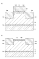
図1は、本発明の一実施形態に係る高電子移動度トランジスタ(HEMT)1Aの構成を示す断面図である。HEMT1Aは、基板11、バッファ層13、電子走行層(チャネル層)14、障壁層(電子供給層)15、二つの高濃度n型半導体領域26a及び26b、ソース電極31、ドレイン電極32、並びにゲート電極33を備える。このHEMT1Aは絶縁性の表面保護膜(不図示)によって覆われており、ソース電極31、ドレイン電極32、及びゲート電極33は、表面保護膜に形成された開口を介して、対応する各金属配線にそれぞれ接続される。
FIG. 1 is a cross-sectional view showing a configuration of a high electron mobility transistor (HEMT) 1A according to an embodiment of the present invention. The HEMT 1A includes a
基板11は、平坦な主面11aを有する結晶成長用の基板である。基板11は、例えばGaN基板、SiC基板、Si基板、及びサファイア基板の何れかとすることができる。バッファ層13は、基板11の主面11a上にエピタキシャル成長した層である。バッファ層13は、例えばAlN又はAlGaNといった、Alを含むIII族窒化物半導体層である。電子走行層14は、主面11a上に設けられ、バッファ層13上にエピタキシャル成長した層である。電子走行層14の厚さは、例えば400nm以上1200nm以下である。電子走行層14は、例えばi型GaN層といったIII族窒化物半導体層である。
The
電子走行層14は、ドライエッチングにより形成された凹部(リセス)14aと、二つの凹部14aに挟まれたメサ構造であるメサ14bとを有する。凹部14aの底面は平坦であり、主面11aと同じ面方位を有する。メサ14bの側面14cは、主面11aの法線に対して傾斜している。側面14cと主面11aの法線との成す角は、例えば20°以上45°以下である。言い換えれば、側面14cと、主面11aに平行な仮想平面との成す角θ2は、例えば45°以上70°以下である。一例では、この角度θ2はGaN結晶の面方位によって決定され、45°もしくは60°である。
The
障壁層15は、電子走行層14上にエピタキシャル成長した層であって、メサ14b上に設けられている。障壁層15は、電子走行層14よりも大きなバンドギャップを有するIII族窒化物半導体層である。このようなIII族窒化物半導体層としては、例えばi型AlGaN層またはi型InAlN層が挙げられる。障壁層15の厚さは、例えば5nm以上20nm以下であり、一例では8nmである。電子走行層14と障壁層15との界面の電子走行層14側に2次元電子ガス(2DEG)が生じ、これがチャネル領域となる。障壁層15がInAlNからなる場合、そのIn組成は例えば15%以上19%以下であり、電子走行層14との格子整合を考慮して定められる。一例では、障壁層15のIn組成は17%である。
The
高濃度n型半導体領域26a,26bは、電子走行層14の凹部14a上に形成された領域である。高濃度n型半導体領域26aは、メサ14bの一方の側面14c、及び障壁層15の一方の側面に接する。高濃度n型半導体領域26bは、メサ14bの他方の側面14c、及び障壁層15の他方の側面に接する。言い換えれば、電子走行層14のうちメサ14bを構成する一部および障壁層15は、高濃度n型半導体領域26a,26bの間に設けられている。
The high concentration n-
高濃度n型半導体領域26a,26bは、n型のZnO系化合物半導体領域であり、一例ではn型ZnO若しくはn型ZnMgOからなる。また、高濃度n型半導体領域26a,26bには、n型不純物としてのAl及びGaの少なくとも一方が高濃度でドープされている。高濃度n型半導体領域26a,26bの電子濃度は、例えば1×1019cm-3以上である。
The high-concentration n-
高濃度n型半導体領域26a,26bの厚さは、メサ14bの高さと障壁層15の厚さとを合わせた厚さよりも厚い。高濃度n型半導体領域26a,26bの厚さは例えば50nm以上200nm以下であり、一例では120nmである。従って、主面11aから測った障壁層15の表面の水平位置H1は、高濃度n型半導体領域26a,26bの各表面の水平位置H2よりも低い。
The thickness of the high-concentration n-
後述するように、障壁層15は、高濃度n型半導体領域26a,26bのウェットエッチングによりその表面を露出する。このエッチングの際、高濃度n型半導体領域26a,26bの表面のうち障壁層15に隣接する一部の表面26cは、主面11aの法線に対して大きく傾斜して形成される。表面26cと障壁層15の表面との成す角θ1は、135°以上160°以下の範囲内にある。言い換えれば、障壁層15の表面に平行な仮想面と、表面26cとの成す角は、20°以上45°以下の範囲内にある。
As will be described later, the surface of the
ソース電極31、ゲート電極33、及びドレイン電極32は、この順に並んで形成されている。ソース電極31は、一方の高濃度n型半導体領域26a上に設けられて該高濃度n型半導体領域26aとオーミック接触を成す。ドレイン電極32は、他方の高濃度n型半導体領域26b上に設けられて該高濃度n型半導体領域26bとオーミック接触を成す。ゲート電極33は、障壁層15上であって高濃度n型半導体領域26aと高濃度n型半導体領域26bとの間の領域上に設けられる。ゲート電極33は、ゲート抵抗を下げるために断面T字状に形成されている。
The
以上の構成を備える本実施形態のHEMT1Aの製造方法について、図2〜図4を参照しながら説明する。まず、図2(a)に示されるように、基板11上にバッファ層13、電子走行層14、及び障壁層15を順に成長する。具体的には、基板11をMOCVD装置内に配置して、トリメチルアルミニウム(TMA)及びNH3を装置内に供給し、基板11上にAlNバッファ層13をエピタキシャル成長する。このときの成長温度は例えば1000℃〜1200℃であり、一例では1080℃である。次に、トリメチルガリウム(TMG)及びNH3を供給し、AlNバッファ層13上にGaN電子走行層14をエピタキシャル成長する。このときの成長温度は例えば1000℃〜1100℃であり、一例では1080℃である。これら二つの層13,14を成長する時の装置内の圧力は例えば13.3kPaである。
A method for manufacturing the
続いて、GaN電子走行層14上に障壁層15をエピタキシャル成長する。障壁層15がInAlNからなる場合、トリメチルインジウム(TMI)、TMA及びNH3を供給する。成長温度は例えば650℃〜850℃であり、一例では800℃である。圧力は例えば15.0kPaである。また、障壁層15がAlGaNからなる場合、TMA、TMG及びNH3を供給する。成長温度は例えば1000℃〜1200℃であり、一例では1080℃である。圧力は例えば13.3kPaである。こうして、バッファ層13、電子走行層14、及び障壁層15を基板11上に有する基板生産物を作製する。
Subsequently, the
続いて、上記の基板生産物をMOCVD装置から取り出し、反応性イオンエッチング(RIE:Reactive Ion Etching)装置内に移す。そして、例えば塩素系ガスを反応ガスとするRIEによって、前述の障壁層15及び電子走行層14をそれぞれ含む二つの領域A1,A2を除去する。特に、電子走行層14がi型GaN層であり、障壁層15がi型InAlN層である場合には、例えばCl2及びBCl3のうち少なくとも一方を用いたRIEを行う。こうして、図2(b)に示されるように、凹部14aと、この凹部14aに挟まれたメサ14bとが形成される。このとき、エッチング条件(塩素ガスの混合比、圧力等)を調節することにより、メサ14bの側面14cを主面11aの法線に対して傾斜させる(好適には45°の角度で形成する)。エッチング条件の一例としては、Cl2ガス流量:5ssm、BCl3ガス流量:30sccm、圧力:0.4Pa、プラズマ周波数:13.56MHz、RFパワー:150Wである。凹部14aの深さ(エッチング深さ)は、障壁層15の表面から少なくとも80nmである。
Subsequently, the substrate product is taken out of the MOCVD apparatus and transferred into a reactive ion etching (RIE) apparatus. Then, for example, the two regions A1 and A2 including the
続いて、基板生産物をRIE装置から取り出し、基板生産物の表面を洗浄する。具体的には、基板生産物の表面、すなわち障壁層15の表面およびエッチングにより露出した凹部14aの表面に対し、HFまたはHClを用いて洗浄を行う。
Subsequently, the substrate product is taken out from the RIE apparatus, and the surface of the substrate product is cleaned. Specifically, the surface of the substrate product, that is, the surface of the
続いて、図3(a)に示されるように、主面11aの全面(すなわち凹部14a及びメサ14b上)に、分子線エピタキシー(MBE)法を用いて、高濃度n型半導体層26を成長させる。このとき、n型不純物としてのAl及びGaの少なくとも一方を高濃度(例えば1×1019cm-3以上)でドープする。高濃度n型半導体層26の厚さは例えば120nmである。高濃度n型半導体層26がn型ZnO層の場合、例えば亜鉛(Zn)の固体原料を用い、O2プラズマ雰囲気中で高濃度n型半導体層26を気相成長する。このときの成長温度は、例えば600℃である。
Subsequently, as shown in FIG. 3A, a high-concentration n-
続いて、高濃度n型半導体層26の熱処理を行う。熱処理温度は例えば600℃以上800℃以下である。一例では、O2雰囲気下で800℃30分の熱処理を行う。
Subsequently, heat treatment of the high-concentration n-
続いて、通常のリソグラフィー技術及びリフトオフ技術を用いて、メサ14bを挟む高濃度n型半導体層26上の領域のそれぞれに、ソース電極31及びドレイン電極32を形成する。ソース電極31及びドレイン電極32は、例えばIn/Au積層金属である。その後、この積層金属を熱処理してそれぞれソース電極31、ドレイン電極32とする。熱処理の温度は例えば350℃である。
Subsequently, the
続いて、図3(b)に示されるように、通常のリソグラフィー技術を用いて、高濃度n型半導体層26上にレジストマスク64を形成する。レジストマスク64は、メサ14b上に開口64aを有する。この開口64aは例えばEB露光技術を用いて形成され、その幅は例えば0.1μmである。レジストマスク64の厚さは例えば300nmである。
Subsequently, as shown in FIG. 3B, a resist
続いて、レジストマスク64の開口64aを通じてメサ14b上の高濃度n型半導体層26をウェットエッチングにより除去し、図4(a)に示されるように、傾斜した表面26cを有する高濃度n型半導体領域26a,26bを形成する。上述したように、表面26cと障壁層15の表面との成す角θ1は135°〜160°である。高濃度n型半導体層26がn型のZnO系化合物半導体層の場合には、このような表面26cの角度を実現するために、エッチャントとして例えば希釈クエン酸、希釈アコニット酸、及び酢酸のうち少なくとも一つが用いられる。
Subsequently, the high concentration n-
続いて、図4(b)に示されるように、レジストマスク64を利用して、メサ14b上にゲート電極33を形成する。このとき、ゲート電極33の下部はレジストマスク64の開口64aを充填し、ウェットエッチングにより生じた空隙を通って障壁層15に達する。また、ゲート電極33の上部はレジストマスク64上に拡がる。これにより、ゲート電極33は断面T字状となる。ゲート電極33は、例えばNi/Auからなる。最後に、レジストマスク64を除去し、例えば原子層堆積(ALD)法を用いてAl2O3を形成し、半導体の表面を保護する。以上の各工程を経て、図1に示される本実施形態のHEMT1Aが完成する。
Subsequently, as illustrated in FIG. 4B, the
以上に説明した、本実施形態によるHEMT1A及びその製造方法によって得られる効果について説明する。HEMT1A及びその製造方法では、障壁層15および電子走行層14のうちゲート電極33の下に位置する部分の両側の一対の部分を除去し、除去後の領域(リセス)に高濃度n型半導体領域26a,26bを形成し、該高濃度n型半導体領域26a,26b上にソース電極31及びドレイン電極32を形成する。これにより、高濃度n型半導体領域26a,26bが障壁層15と電子走行層14との界面に直接接するので、アクセス抵抗を低減することができる。
The effects obtained by the
ここで、図5〜図7は、比較例に係るHEMTの製造方法を示す断面図である。まず、図5(a)に示されるように、基板11上においてバッファ層13、電子走行層14、及び障壁層15を順に成長する。このときの具体的方法は本実施形態と同様である。
Here, FIG. 5 to FIG. 7 are cross-sectional views showing a method for manufacturing a HEMT according to a comparative example. First, as shown in FIG. 5A, the
次に、例えば塩素系ガスを反応ガスとするRIEによって、領域A3,A4を除去する。領域A3,A4は、それぞれ電子走行層14及び障壁層15の一部を含む。こうして、図5(b)に示されるように、凹部(リセス)102と、凹部102に挟まれたメサ104が形成される。本実施形態のメサ14b(図2(b)参照)と異なり、比較例に係るメサ104の側面104aは、凹部102の底面に対して略垂直である。
Next, the regions A3 and A4 are removed by RIE using, for example, a chlorine-based gas as a reaction gas. Regions A3 and A4 include part of the
続いて、表面を洗浄したのち、図6(a)に示されるように、メサ104上にマスク106を形成する。マスク106は、例えばSiO2からなり、SiO2膜を主面11a上の全面(凹部102上及びメサ104上)に成膜したのち、凹部102上のSiO2膜を、例えばフッ素系ガス(SF6またはCF4)を用いたRIEにより除去して形成される。そして、例えばMOCVD法を用いて、高濃度n型GaN層108を凹部102上に選択成長する。このとき、TMGとNH3を原料としてSiH4をドーパントとする。また、成長後の高濃度n型GaN層108の厚さは例えば120nmであり、不純物濃度は例えば1×1019cm-3である。成長温度は例えば1000℃であり、圧力は例えば20.0kPaである。その後、HF溶液に例えば10分程度浸漬して、図6(b)に示されるようにマスク106を除去し、メサ104上の高濃度n型GaN層108を除去する。
Subsequently, after the surface is cleaned, a
続いて、図7に示されるように、通常のリソグラフィー技術及びリフトオフ技術を用いて、メサ104を挟む高濃度n型GaN層108上の領域に、ソース電極31及びドレイン電極32を形成する。そして、ソース電極31及びドレイン電極32の間の障壁層15上にSiN保護膜110を形成し、EB露光技術を用いてメサ104上に開口部110aを形成する。SiN膜110の厚さは例えば100nmである。次いで、ゲート電極33を形成して開口部110aを塞ぐ。以上で、比較例に係るHEMT100が完成する。
Subsequently, as shown in FIG. 7, the
この比較例では、選択成長におけるマストランスポート(選択成長マスクの近傍が厚く形成される現象)に起因して、メサ104近傍の高濃度n型GaN層108の厚さが例えば200nmに近くなり、障壁層15の表面に対して100nm以上盛り上がる。その結果、ゲート電極33と高濃度n型GaN層108との間隔が短くなり、ゲート・ドレイン間の耐圧性能の低下、及びゲート・ソース間の容量の増大を招く。
In this comparative example, due to mass transport in selective growth (a phenomenon in which the vicinity of the selective growth mask is formed thick), the thickness of the high-concentration n-
この比較例において、ゲート電極33のゲート長(Lg)を0.1μmとし、ソース電極31とドレイン電極32との間隔を0.8μmとし、ゲート電極33の上部の幅を0.6μmとして、高周波特性を評価した。その結果、遮断周波数(ft)は120GHzであり、そのときのゲート・ソース間の容量Cgsは0.6pF/mmであった。この容量Cgsの値はゲート長に比較して大きく、ゲート電極33と高濃度n型GaN層108との間隔が短くなっていることがその一因であると考えられる。
In this comparative example, the gate length (Lg) of the
これに対し、本実施形態のHEMT1Aにおいて、ゲート電極33のゲート長(Lg)、ソース電極31とドレイン電極32との間隔、及びゲート電極33の上部の幅を上記と等しくして、高周波特性を評価した。その結果、遮断周波数(ft)は180GHzに向上し、そのときのゲート・ソース間の容量Cgsは0.4pF/mmであった。この容量Cgsの値は、ゲート長(0.1μm)からすれば適度な値である。
On the other hand, in the
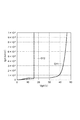
また、図8は、ゲート・ドレイン間の耐圧性能を示すグラフであって、グラフG11は本実施形態のHEMT1Aに関する特性を示し、グラフG12は比較例のHEMT100に関する特性を示す。縦軸はゲート・ドレイン間電流Igd(A/mm)を示し、横軸はゲート・ドレイン間電圧Vgd(V)を示す。グラフG12に示される比較例では、ゲート・ドレイン間の耐圧が16Vと低く、耐圧測定時にゲート・ドレイン間の短絡が生じた。ドレイン側の高濃度n型GaN層108とゲート電極33との短絡が生じていた。これに対し、グラフG11に示される本実施形態のHEMT1Aでは、ゲート・ドレイン間の耐圧が40V以上と高く、ゲート・ドレイン間電流が1mmA/mmを超えてもHEMT1Aのショート故障は生じなかった。
FIG. 8 is a graph showing the breakdown voltage performance between the gate and the drain. The graph G11 shows the characteristics related to the
本実施形態では、高濃度n型半導体領域26a,26bの表面26cと障壁層15の表面との成す角θ1が135°〜160°と大きい(すなわち主面11aの法線方向に対して表面26cが大きく傾斜している)ことにより、ゲート電極33と高濃度n型半導体領域26a,26bとの距離が比較例よりも広い。すなわち、高濃度n型半導体領域26a,26bがゲート電極33から距離をもって形成されているので、上述したように、ゲート・ドレイン間の耐圧性能の低下、及びゲート・ソース間の容量の増大を効果的に抑えることができる。
In the present embodiment, an angle θ1 formed by the
また、表面26cと障壁層15の表面との成す角θ1が大きく、高濃度n型半導体層26をエッチングする工程におけるエッチング量のマージンを大きくすることができる。同様の理由により、フォトリソグラフィー技術における位置精度が低くても表面26cの形成位置のずれを抑えることができる。これらのことから、ソース・ドレイン間の距離を狭くした微細構造においても、高い量産性を実現できる。
Further, the angle θ1 formed by the
また、本実施形態のように、高濃度n型半導体領域26a,26bはn型のZnO系化合物半導体領域であってもよい。この場合、n型GaNを用いる場合よりも低いアクセス抵抗及びコンタクト抵抗を実現することができる。その結果、相互コンダクタンスgm及び遮断周波数ftを格段に高めることができる。
Further, as in the present embodiment, the high-concentration n-
なお、高濃度n型半導体領域26a,26bの構成材料は、十分に大きな導電率を有し、電子走行層14に対して大きなヘテロ障壁を形成しなければ、他の材料でも良い。また、障壁層15に対するエッチングの選択性と、大きな角度θ1でのエッチングを可能とする化学的特性とを充足する材料であれば、本実施形態のHEMT1Aの構造を好適に実現できる。このような条件を満たす材料としては、次に示される酸化物半導体が好適である。すなわち酸化物半導体とは、上述したZnOの他、In2O3、SnO2、CdO、TiO2、並びにこれらの混晶(例えばITO:In−Sn−O)のうち少なくとも一つを指す。これらの酸化物半導体は、低い電気抵抗を有する。また、混晶比を調整することにより、電子走行層14との電子障壁を低減できる。更に、酸化物であるから一般的には酸に可溶であり、適切なエッチャントを用いてウェットエッチングを行うことが可能である。従って、本実施形態の高濃度n型半導体領域26a,26bの形状を好適に実現できる。
The constituent material of the high-concentration n-
また、本実施形態のように、基板11をGaN基板、SiC基板、Si基板、及びサファイア基板のうち何れかとし、電子走行層14をi型GaN層とし、障壁層15をi型InAlN層とすることができる。これにより、広いバンドギャップを有し、極めて大きな絶縁破壊電圧及び飽和電子速度を有するGaN系HEMTを実現できる。また障壁層15の上部に、障壁層15よりもバンドギャップの小さい(例えばGaN)半導体層、いわゆるキャップ層を含む構造を用いても良い。
Further, as in the present embodiment, the
また、本実施形態のように、ゲート電極33を形成する工程において、高濃度n型半導体層26をエッチングするためのレジストマスク64を再利用してゲート電極33を形成してもよい。これにより、工程数を少なくすることができる。
Further, as in this embodiment, in the step of forming the
また、本実施形態のように、高濃度n型半導体層26がn型のZnO系化合物半導体層の場合、高濃度n型半導体領域26a,26bを形成する工程において、エッチャントとして希釈クエン酸、希釈アコニット酸、及び酢酸のうち少なくとも一つを用いることができる。これにより、高濃度n型半導体領域26a,26bの表面26cと障壁層15の表面との成す角θ1を、135°〜160°といった大きな角度にすることができる。
Further, as in the present embodiment, when the high concentration n-
また、本実施形態のように、電子走行層14がi型GaN層であり、障壁層15がi型InAlN層である場合、Cl2及びBCl3のうち少なくとも一方を用いたドライエッチングによりメサ14bを形成することができる。
Further, as in the present embodiment, when the
本発明による高電子移動度トランジスタ、及び高電子移動度トランジスタの製造方法は、上述した実施形態に限られるものではなく、他に様々な変形が可能である。例えば、上記実施形態ではGaN系のHEMTを例示したが、本発明はこれ以外にも様々な半導体材料のHEMTに適用することができる。 The high electron mobility transistor and the method for manufacturing the high electron mobility transistor according to the present invention are not limited to the above-described embodiments, and various other modifications are possible. For example, although the GaN-based HEMT has been exemplified in the above embodiment, the present invention can be applied to HEMTs of various semiconductor materials other than this.
また、上記実施形態では、高濃度n型半導体層をエッチングするためのレジストマスクを再利用してゲート電極を形成しているが、高濃度n型半導体層をエッチングしたのちにレジストマスクを一旦除去し、ゲート電極を形成するためのマスクを再度形成したのち、ゲート電極を形成してもよい。 In the above embodiment, the gate electrode is formed by reusing the resist mask for etching the high-concentration n-type semiconductor layer. However, after the high-concentration n-type semiconductor layer is etched, the resist mask is temporarily removed. The gate electrode may be formed after the mask for forming the gate electrode is formed again.
11…基板、11a…主面、13…バッファ層、14…電子走行層、14a…凹部、14b…メサ、14c…側面、15…障壁層、26…高濃度n型半導体層、26a,26b…高濃度n型半導体領域、31…ソース電極、32…ドレイン電極、33…ゲート電極、64…レジストマスク、64a…開口。
DESCRIPTION OF
Claims (7)
前記主面上に設けられ、メサ構造を有する電子走行層と、
前記メサ構造上に設けられ、前記電子走行層よりも大きいバンドギャップを有する障壁層と、
前記電子走行層上に設けられ、前記メサ構造及び前記障壁層の側面にそれぞれ接する二つの高濃度n型半導体領域と、
一方の前記高濃度n型半導体領域上に設けられたソース電極と、
他方の前記高濃度n型半導体領域上に設けられたドレイン電極と、
前記障壁層上に設けられたゲート電極と、
を備え、
前記障壁層の表面の水平位置は、前記高濃度n型半導体領域の各表面の水平位置よりも低く、
各高濃度n型半導体領域の前記表面のうち前記障壁層に隣接する一部と、前記障壁層の前記表面との成す角が135°以上160°以下の範囲内にある、高電子移動度トランジスタ。 A substrate having a main surface;
An electron transit layer provided on the main surface and having a mesa structure;
A barrier layer provided on the mesa structure and having a larger band gap than the electron transit layer;
Two high-concentration n-type semiconductor regions provided on the electron transit layer and in contact with side surfaces of the mesa structure and the barrier layer,
A source electrode provided on one of the high-concentration n-type semiconductor regions;
A drain electrode provided on the other high-concentration n-type semiconductor region;
A gate electrode provided on the barrier layer;
With
The horizontal position of the surface of the barrier layer is lower than the horizontal position of each surface of the high-concentration n-type semiconductor region,
A high electron mobility transistor in which an angle formed between a part of the surface of each high-concentration n-type semiconductor region adjacent to the barrier layer and the surface of the barrier layer is in a range of 135 ° to 160 °. .
前記障壁層及び前記電子走行層をエッチングすることによりメサ構造を形成する工程と、
前記主面上に高濃度n型半導体層を形成する工程と、
前記メサ構造上に開口を有するマスクを前記高濃度n型半導体層上に形成する工程と、
前記マスクの前記開口を通じて前記メサ構造上の前記高濃度n型半導体層にウェットエッチングを施すことにより、高濃度n型半導体領域を形成する工程と、
前記メサ構造上にゲート電極を形成する工程と、
を含む、高電子移動度トランジスタの製造方法。 A step of sequentially growing an electron transit layer and a barrier layer having a larger band gap than the electron transit layer on a main surface of the substrate;
Forming a mesa structure by etching the barrier layer and the electron transit layer;
Forming a high-concentration n-type semiconductor layer on the main surface;
Forming a mask having an opening on the mesa structure on the high-concentration n-type semiconductor layer;
Forming a high-concentration n-type semiconductor region by performing wet etching on the high-concentration n-type semiconductor layer on the mesa structure through the opening of the mask;
Forming a gate electrode on the mesa structure;
A method of manufacturing a high electron mobility transistor.
前記高濃度n型半導体領域を形成する工程において、エッチャントとして希釈クエン酸、希釈アコニット酸、及び酢酸のうち少なくとも一つを用いる、請求項4または5に記載の高電子移動度トランジスタの製造方法。 The high-concentration n-type semiconductor layer is an n-type ZnO-based compound semiconductor layer;
6. The method of manufacturing a high electron mobility transistor according to claim 4, wherein in the step of forming the high concentration n-type semiconductor region, at least one of diluted citric acid, diluted aconitic acid, and acetic acid is used as an etchant.
Cl2及びBCl3のうち少なくとも一方を用いたドライエッチングにより前記メサ構造を形成する、請求項4〜6のいずれか一項に記載の高電子移動度トランジスタの製造方法。 The electron transit layer is an i-type GaN layer, and the barrier layer is an i-type InAlN layer;
Cl to form the mesa structure by dry etching using at least one of 2 and BCl 3, the manufacturing method of the high electron mobility transistor according to any one of claims 4-6.
Priority Applications (2)
| Application Number | Priority Date | Filing Date | Title |
|---|---|---|---|
| JP2016048292A JP6690320B2 (en) | 2016-03-11 | 2016-03-11 | High electron mobility transistor and method of manufacturing high electron mobility transistor |
| US15/456,226 US10147811B2 (en) | 2016-03-11 | 2017-03-10 | Process of forming a high electron mobility transistor (HEMT) |
Applications Claiming Priority (1)
| Application Number | Priority Date | Filing Date | Title |
|---|---|---|---|
| JP2016048292A JP6690320B2 (en) | 2016-03-11 | 2016-03-11 | High electron mobility transistor and method of manufacturing high electron mobility transistor |
Publications (2)
| Publication Number | Publication Date |
|---|---|
| JP2017163082A true JP2017163082A (en) | 2017-09-14 |
| JP6690320B2 JP6690320B2 (en) | 2020-04-28 |
Family
ID=59787133
Family Applications (1)
| Application Number | Title | Priority Date | Filing Date |
|---|---|---|---|
| JP2016048292A Active JP6690320B2 (en) | 2016-03-11 | 2016-03-11 | High electron mobility transistor and method of manufacturing high electron mobility transistor |
Country Status (2)
| Country | Link |
|---|---|
| US (1) | US10147811B2 (en) |
| JP (1) | JP6690320B2 (en) |
Cited By (1)
| Publication number | Priority date | Publication date | Assignee | Title |
|---|---|---|---|---|
| JP2021027165A (en) * | 2019-08-05 | 2021-02-22 | 富士通株式会社 | Semiconductor device, manufacturing method of semiconductor device, and electronic system |
Families Citing this family (7)
| Publication number | Priority date | Publication date | Assignee | Title |
|---|---|---|---|---|
| US10388753B1 (en) * | 2017-03-31 | 2019-08-20 | National Technology & Engineering Solutions Of Sandia, Llc | Regrowth method for fabricating wide-bandgap transistors, and devices made thereby |
| JP6828595B2 (en) * | 2017-05-29 | 2021-02-10 | 三菱電機株式会社 | Manufacturing method of semiconductor devices |
| JP7013710B2 (en) * | 2017-08-07 | 2022-02-01 | 住友電気工業株式会社 | Manufacturing method of nitride semiconductor transistor |
| JP6977449B2 (en) * | 2017-09-27 | 2021-12-08 | 住友電気工業株式会社 | Manufacturing method of field effect transistor and field effect transistor |
| JP6879177B2 (en) * | 2017-11-24 | 2021-06-02 | 住友電気工業株式会社 | Nitride semiconductor device manufacturing method |
| CN110112207B (en) * | 2019-05-20 | 2020-05-05 | 中山大学 | Gallium oxide-based mixed PiN Schottky diode and preparation method thereof |
| WO2023010583A1 (en) * | 2021-08-06 | 2023-02-09 | 华为技术有限公司 | Integrated circuit, power amplification circuit and electronic device |
Citations (11)
| Publication number | Priority date | Publication date | Assignee | Title |
|---|---|---|---|---|
| JPH03211839A (en) * | 1989-12-31 | 1991-09-17 | Samsung Electron Co Ltd | Compound semiconductor device and method of manufacturing the same |
| JPH03250741A (en) * | 1990-02-28 | 1991-11-08 | Fujitsu Ltd | Manufacture of semiconductor device |
| JPH05343435A (en) * | 1992-06-08 | 1993-12-24 | Hitachi Ltd | Semiconductor device |
| JPH0661268A (en) * | 1992-04-30 | 1994-03-04 | Mitsubishi Kasei Corp | Compound semiconductor device with selective regrowth region and its manufacture |
| JPH06267992A (en) * | 1993-03-11 | 1994-09-22 | Hitachi Ltd | Semiconductor device and its manufacture |
| JPH0888238A (en) * | 1994-09-20 | 1996-04-02 | Hitachi Ltd | Compound semiconductor field effect transistor and compound semiconductor integrated circuit using thereof |
| JP2006313845A (en) * | 2005-05-09 | 2006-11-16 | Rohm Co Ltd | Nitride semiconductor element and its fabrication process |
| JP2007317856A (en) * | 2006-05-25 | 2007-12-06 | Mitsubishi Gas Chem Co Inc | Etching liquid composition and etching method |
| JP2007538402A (en) * | 2004-05-20 | 2007-12-27 | クリー インコーポレイテッド | Method for fabricating nitride-based transistor with regrowth ohmic contact region and nitride-based transistor with regrowth ohmic contact region |
| JP2008098455A (en) * | 2006-10-13 | 2008-04-24 | Eudyna Devices Inc | Semiconductor device |
| JP2015523733A (en) * | 2012-07-13 | 2015-08-13 | レイセオン カンパニー | Gallium nitride devices with low ohmic contact resistance |
Family Cites Families (6)
| Publication number | Priority date | Publication date | Assignee | Title |
|---|---|---|---|---|
| JP2006261642A (en) | 2005-02-17 | 2006-09-28 | Matsushita Electric Ind Co Ltd | Field effect transistor and method of fabricating the same |
| US7714359B2 (en) | 2005-02-17 | 2010-05-11 | Panasonic Corporation | Field effect transistor having nitride semiconductor layer |
| JP5076278B2 (en) * | 2005-03-14 | 2012-11-21 | 日亜化学工業株式会社 | Field effect transistor |
| JP2012054471A (en) * | 2010-09-02 | 2012-03-15 | Fujitsu Ltd | Semiconductor device, method of manufacturing the same, and power supply device |
| JP2012084739A (en) * | 2010-10-13 | 2012-04-26 | Sumitomo Electric Ind Ltd | Semiconductor device and method of manufacturing the same |
| US8324037B1 (en) * | 2011-09-28 | 2012-12-04 | Ishiang Shih | Fabrication methods for HEMT devices and circuits on compound semiconductor materials |
-
2016
- 2016-03-11 JP JP2016048292A patent/JP6690320B2/en active Active
-
2017
- 2017-03-10 US US15/456,226 patent/US10147811B2/en active Active
Patent Citations (11)
| Publication number | Priority date | Publication date | Assignee | Title |
|---|---|---|---|---|
| JPH03211839A (en) * | 1989-12-31 | 1991-09-17 | Samsung Electron Co Ltd | Compound semiconductor device and method of manufacturing the same |
| JPH03250741A (en) * | 1990-02-28 | 1991-11-08 | Fujitsu Ltd | Manufacture of semiconductor device |
| JPH0661268A (en) * | 1992-04-30 | 1994-03-04 | Mitsubishi Kasei Corp | Compound semiconductor device with selective regrowth region and its manufacture |
| JPH05343435A (en) * | 1992-06-08 | 1993-12-24 | Hitachi Ltd | Semiconductor device |
| JPH06267992A (en) * | 1993-03-11 | 1994-09-22 | Hitachi Ltd | Semiconductor device and its manufacture |
| JPH0888238A (en) * | 1994-09-20 | 1996-04-02 | Hitachi Ltd | Compound semiconductor field effect transistor and compound semiconductor integrated circuit using thereof |
| JP2007538402A (en) * | 2004-05-20 | 2007-12-27 | クリー インコーポレイテッド | Method for fabricating nitride-based transistor with regrowth ohmic contact region and nitride-based transistor with regrowth ohmic contact region |
| JP2006313845A (en) * | 2005-05-09 | 2006-11-16 | Rohm Co Ltd | Nitride semiconductor element and its fabrication process |
| JP2007317856A (en) * | 2006-05-25 | 2007-12-06 | Mitsubishi Gas Chem Co Inc | Etching liquid composition and etching method |
| JP2008098455A (en) * | 2006-10-13 | 2008-04-24 | Eudyna Devices Inc | Semiconductor device |
| JP2015523733A (en) * | 2012-07-13 | 2015-08-13 | レイセオン カンパニー | Gallium nitride devices with low ohmic contact resistance |
Cited By (1)
| Publication number | Priority date | Publication date | Assignee | Title |
|---|---|---|---|---|
| JP2021027165A (en) * | 2019-08-05 | 2021-02-22 | 富士通株式会社 | Semiconductor device, manufacturing method of semiconductor device, and electronic system |
Also Published As
| Publication number | Publication date |
|---|---|
| US20170263743A1 (en) | 2017-09-14 |
| JP6690320B2 (en) | 2020-04-28 |
| US10147811B2 (en) | 2018-12-04 |
Similar Documents
| Publication | Publication Date | Title |
|---|---|---|
| JP6690320B2 (en) | High electron mobility transistor and method of manufacturing high electron mobility transistor | |
| US9379191B2 (en) | High electron mobility transistor including an isolation region | |
| JP6018360B2 (en) | Compound semiconductor device and manufacturing method thereof | |
| JP5495257B2 (en) | Group III nitride field effect transistor and method of manufacturing the same | |
| US11908927B2 (en) | Nitride semiconductor device | |
| US20160233311A1 (en) | Manufacturing method of semiconductor device and semiconductor device | |
| US10784361B2 (en) | Semiconductor device and method for manufacturing the same | |
| JP2010192633A (en) | METHOD FOR MANUFACTURING GaN-BASED FIELD-EFFECT TRANSISTOR | |
| JP2011044647A (en) | Group-iii nitride-based field-effect transistor and method of manufacturing the same | |
| US10700189B1 (en) | Semiconductor devices and methods for forming the same | |
| US20130168686A1 (en) | High electron mobility transistor and method of forming the same | |
| US10211323B2 (en) | Hemt having heavily doped N-type regions and process of forming the same | |
| JP2017059671A (en) | High electron mobility transistor and method for manufacturing high electron mobility transistor | |
| JP6597046B2 (en) | High electron mobility transistor | |
| US20160359035A1 (en) | Semiconductor structure and method of forming the same | |
| JP6977449B2 (en) | Manufacturing method of field effect transistor and field effect transistor | |
| JP2017514316A (en) | Heterojunction field effect transistor | |
| JP2011171440A (en) | Group iii nitride-based hetero field-effect transistor | |
| JP5379391B2 (en) | Semiconductor device comprising gallium nitride compound semiconductor and method for manufacturing the same | |
| US10373833B2 (en) | Semiconductor device and method for manufacturing the same | |
| KR101668445B1 (en) | Semiconductor device and manufacturing method thereof | |
| JP2014229767A (en) | Heterojunction field effect transistor and method for manufacturing the same | |
| EP3405979B1 (en) | Semiconductor device, electronic part, electronic apparatus, and method for fabricating semiconductor device | |
| US20230043312A1 (en) | Method for manufacturing nitride semiconductor device and nitride semiconductor device | |
| US20150249150A1 (en) | Transistor having nitride semiconductor used therein and method for manufacturing transistor having nitride semiconductor used therein |
Legal Events
| Date | Code | Title | Description |
|---|---|---|---|
| A621 | Written request for application examination |
Free format text: JAPANESE INTERMEDIATE CODE: A621 Effective date: 20181221 |
|
| A977 | Report on retrieval |
Free format text: JAPANESE INTERMEDIATE CODE: A971007 Effective date: 20190905 |
|
| A131 | Notification of reasons for refusal |
Free format text: JAPANESE INTERMEDIATE CODE: A131 Effective date: 20190910 |
|
| A601 | Written request for extension of time |
Free format text: JAPANESE INTERMEDIATE CODE: A601 Effective date: 20191111 |
|
| A521 | Request for written amendment filed |
Free format text: JAPANESE INTERMEDIATE CODE: A523 Effective date: 20191210 |
|
| TRDD | Decision of grant or rejection written | ||
| A01 | Written decision to grant a patent or to grant a registration (utility model) |
Free format text: JAPANESE INTERMEDIATE CODE: A01 Effective date: 20200310 |
|
| A61 | First payment of annual fees (during grant procedure) |
Free format text: JAPANESE INTERMEDIATE CODE: A61 Effective date: 20200323 |
|
| R150 | Certificate of patent or registration of utility model |
Ref document number: 6690320 Country of ref document: JP Free format text: JAPANESE INTERMEDIATE CODE: R150 |
|
| R250 | Receipt of annual fees |
Free format text: JAPANESE INTERMEDIATE CODE: R250 |
|
| R250 | Receipt of annual fees |
Free format text: JAPANESE INTERMEDIATE CODE: R250 |