JP2017137523A - Semiconductor wafer - Google Patents
Semiconductor wafer Download PDFInfo
- Publication number
- JP2017137523A JP2017137523A JP2016017434A JP2016017434A JP2017137523A JP 2017137523 A JP2017137523 A JP 2017137523A JP 2016017434 A JP2016017434 A JP 2016017434A JP 2016017434 A JP2016017434 A JP 2016017434A JP 2017137523 A JP2017137523 A JP 2017137523A
- Authority
- JP
- Japan
- Prior art keywords
- wafer
- plating
- semiconductor wafer
- semiconductor
- jig
- Prior art date
- Legal status (The legal status is an assumption and is not a legal conclusion. Google has not performed a legal analysis and makes no representation as to the accuracy of the status listed.)
- Granted
Links
Images


Abstract
Description
この発明は、半導体ウェハに略均一に金属めっき(特に、銀めっき、ニッケルめっき等)を積層した半導体ウェハ、かかる半導体ウェハを製造するための半導体ウェハめっき用治具及びかかる治具を用いた半導体ウェハのめっき処理方法に関し、これらの治具や方法によって製造した半導体ウェハを用いた半導体装置、また、この半導体装置を有する通信機器、電子機器、映像機器、家電機器等に関する。 The present invention relates to a semiconductor wafer in which metal plating (especially, silver plating, nickel plating, etc.) is laminated substantially uniformly on a semiconductor wafer, a semiconductor wafer plating jig for manufacturing such a semiconductor wafer, and a semiconductor using such a jig The present invention relates to a wafer plating method, and relates to a semiconductor device using a semiconductor wafer manufactured by these jigs and methods, and a communication device, electronic device, video device, home appliance, and the like having the semiconductor device.
従来、半導体ウェハの半導体の実装面(半導体を実装する面であり、以下、表面という)に金属(例えば、金、銀、プラチナ、銅等)のめっきをするために、電解(電気)めっき方法を用いることが良く知られている。 Conventionally, an electrolytic (electric) plating method for plating a metal (for example, gold, silver, platinum, copper, etc.) on a semiconductor mounting surface (a surface on which a semiconductor is mounted, hereinafter referred to as a surface) of a semiconductor wafer. Is well known.
このような、半導体ウェハの表面に対する電解(電気)めっきを施すめっき装置の電解めっきの工程において、安定した給電が可能な半導体装置の製造方法が開示されている(特許文献1参照)。 A method of manufacturing a semiconductor device capable of supplying stable power in such a step of electrolytic plating of a plating apparatus that performs electrolytic (electro) plating on the surface of a semiconductor wafer is disclosed (see Patent Document 1).
また、半導体ウェハ等の被めっき体に電気めっきを行う場合に、高電流密度の条件であっても平坦な先端形状のバンプを形成したり、良好な面内均一性を有する金属膜を形成したりすることができるめっき装置が開示されている(特許文献2参照)。 Also, when electroplating an object to be plated such as a semiconductor wafer, a flat tip-shaped bump is formed even under high current density conditions, or a metal film having good in-plane uniformity is formed. A plating apparatus that can be used is disclosed (see Patent Document 2).
上記のような半導体ウェハ等の被めっき物に対するめっき処理時には、半導体ウェハを支持部材で挟持して外部直流電源を用いてめっき槽内の金属イオンのカソード還元により、貴金属のめっき薄膜を形成する電解めっき処理が行われており、電解めっき槽内での搬送めっき処理を迅速に正確に行いやすいようにウェハの支持部材に多種の工夫が施されている。 During the plating process on the object to be plated such as the semiconductor wafer as described above, an electrolysis that forms a noble metal plating thin film by cathodic reduction of metal ions in the plating tank using an external DC power source while holding the semiconductor wafer between support members. A plating process is performed, and various devices are applied to the support member of the wafer so that the transfer plating process in the electrolytic plating tank can be performed quickly and accurately.
しかしながら、特許文献1及び特許文献2に開示されている電解(電気)めっきの技術は、あくまで、半導体ウェハの表面(半導体の実装面)に金属による電気めっき処理を行うものである。ところが、近年では、半導体ウェハの表面だけではなく、半導体ウェハの裏面(半導体の実装面とは反対の面)に金属(金、銀、プラチナ、銅等)をめっきすることが行われている。この半導体ウェハの裏面にめっきする意義は、最終的にウェハ半導体装置の電気導電性(以下、単に導電性という。)を向上し、抵抗値を下げて消費電力の低減を図ることができることにあり、特に昨今のスマートフォン等の通信機器に用いる半導体装置では消費電力の低減は最重要課題の一つになっている。 However, the electrolytic (electro) plating technology disclosed in Patent Document 1 and Patent Document 2 merely performs metal electroplating on the surface of a semiconductor wafer (semiconductor mounting surface). However, in recent years, metal (gold, silver, platinum, copper, etc.) is plated not only on the surface of the semiconductor wafer but also on the back surface of the semiconductor wafer (the surface opposite to the semiconductor mounting surface). The significance of plating on the back surface of the semiconductor wafer is that the electrical conductivity (hereinafter, simply referred to as conductivity) of the wafer semiconductor device can be finally improved, and the resistance value can be lowered to reduce the power consumption. In particular, reduction of power consumption is one of the most important issues in semiconductor devices used in recent communication devices such as smartphones.
そのための半導体ウェハの裏面へのめっき方法としては、スパッタ法や蒸着法を用いて、1〜3μの厚みのめっき被膜を半導体ウェハの裏面に形成している。最終的にウェハ半導体装置の導電性を向上させるためには、従来の1〜3μの金属めっきの被膜を略10μ以上にすることで、さらなる導電性の向上を期待できる。ところが、スパッタ法や蒸着法では、被膜の厚い(例えば、略10μ以上)めっき被膜を半導体ウェハの裏面に形成することはできなかった。そこで、上記の電解(電気)めっきにより、半導体ウェハの裏面に金属めっきの被膜を略10μ以上の厚みで形成することが考えられる。 As a plating method on the back surface of the semiconductor wafer for that purpose, a plating film having a thickness of 1 to 3 μm is formed on the back surface of the semiconductor wafer by sputtering or vapor deposition. In order to finally improve the conductivity of the wafer semiconductor device, further improvement in conductivity can be expected by setting the conventional 1 to 3 μm metal plating film to approximately 10 μm or more. However, in the sputtering method or the vapor deposition method, a thick coating film (for example, approximately 10 μm or more) cannot be formed on the back surface of the semiconductor wafer. Therefore, it is conceivable to form a metal plating film with a thickness of about 10 μm or more on the back surface of the semiconductor wafer by the above electrolytic (electric) plating.
半導体ウェハを支持装置(例えば、ハンガー等)に吊下支持して、循環搬送機器によってハンガーを循環移動しながら外部直流電源を用いて水溶液中の金属イオンをカソード還元で金属薄膜を形成する従来の電解めっき方法では、半導体ウェハの裏面全体に均一に皮膜処理されない場合がある。これは、電解めっきで使われる電流は電極表面の等電位面に垂直に流れることから電極面(被処理面)上での電流分布が不均一となり、被めっき処理物たる円盤の周縁では被膜が厚くなるからである。 Conventionally, a semiconductor wafer is suspended and supported on a support device (for example, a hanger), and a metal thin film is formed by cathodic reduction of metal ions in an aqueous solution using an external DC power source while circulating and moving the hanger with a circulation transfer device. In the electrolytic plating method, the entire back surface of the semiconductor wafer may not be uniformly coated. This is because the current used in electroplating flows perpendicularly to the equipotential surface of the electrode surface, so the current distribution on the electrode surface (surface to be processed) becomes non-uniform, and the coating is not formed on the periphery of the disk that is the object to be plated. This is because it becomes thicker.
このように、単に、電解めっき方法を用いて半導体ウェハの裏面に金属めっきの被膜を略10μ以上の厚みで形成しても、電流密度の高い半導体ウェハ周縁の金属めっきの被膜が厚くなり、電流密度の低い中央部では被膜が薄くなるという欠点を有していた。半導体ウェハの裏面のめっき処理時に膜厚にひずみが生起すると、半導体装置に組み込んだ際に半導体機能に支障を生起し不適格となる。また、均等な膜厚のめっき処理のなされたウェハ部分のみを半導体装置に使用するとウェハ使用の歩留まりが悪くなり不経済となる。 Thus, even if the metal plating film is formed on the back surface of the semiconductor wafer with a thickness of about 10 μm or more simply by using the electrolytic plating method, the metal plating film on the periphery of the semiconductor wafer having a high current density becomes thick. In the central part where the density is low, there is a disadvantage that the coating becomes thin. If the film thickness is distorted during the plating process on the back surface of the semiconductor wafer, the semiconductor function is hindered when incorporated in a semiconductor device, and the semiconductor wafer becomes unqualified. Further, if only a wafer portion that has been subjected to plating treatment with a uniform film thickness is used in a semiconductor device, the yield of using the wafer becomes poor and it becomes uneconomical.
この発明では、半導体ウェハの裏面に形成される導電性の向上のための金属めっきによる被膜を、電解めっき方法を用いて可及的に膜厚にするにもかかわらず略均一に処理することができる半導体ウェハのめっき治具、めっき処理方法、及び、それらのめっき処理がなされた半導体ウェハを用いた半導体装置並びにかかる半導体装置を用いた各種電気機器を提供せんとするものである。 According to the present invention, the metal plating film for improving conductivity formed on the back surface of the semiconductor wafer can be processed substantially uniformly even though the film thickness is made as much as possible using the electrolytic plating method. An object of the present invention is to provide a semiconductor wafer plating jig, a plating method, a semiconductor device using the semiconductor wafer subjected to the plating process, and various electric devices using the semiconductor device.
この発明は、半導体ウェハの裏面全体に略均一に少なくとも2種類以上の異なる種類の金属めっきを積層して構成したことを特徴とする半導体ウェハに関する。 The present invention relates to a semiconductor wafer characterized by laminating at least two or more different types of metal plating substantially uniformly on the entire back surface of the semiconductor wafer.
また、間に半導体ウェハを挟持するように、ウェハ保持盤とそれとは別体のウェハ圧接盤との各盤を圧着固定する圧着治具とより構成し、ウェハ保持盤は、外周縁に懸架部を突設した一定幅員の環状支持板と、環状支持板面に形成した位置決め部と、環状支持板の内周縁部に形成したウェハ保持部と、により構成し、ウェハ圧接盤は、環状支持板の支持板面に圧接する環状板と、環状支持板の位置決め部に嵌着自在となるように環状板面に形成した嵌着部と、より構成してなる請求項1に記載の半導体ウェハを製造するための半導体ウェハめっき用治具に関する。 In addition, it comprises a wafer holding board and a crimping jig for crimping and fixing each board of the wafer pressure welding board separate from the wafer holding board so that the semiconductor wafer is sandwiched between them. Is formed by a fixed-width annular support plate, a positioning part formed on the annular support plate surface, and a wafer holding part formed on the inner peripheral edge of the annular support plate. The semiconductor wafer according to claim 1, comprising: an annular plate that is in pressure contact with the support plate surface; and a fitting portion that is formed on the annular plate surface so as to be freely fitted to a positioning portion of the annular support plate. The present invention relates to a semiconductor wafer plating jig for manufacturing.
また、ウェハ保持盤とウェハ圧接盤との間に圧着治具を介して半導体ウェハを挟持圧着固定してめっき槽中に浸漬し、半導体ウェハ裏面に少なくとも2種類以上の異なる種類の金属めっきを形成し、水洗、乾燥することにも特徴を有する。 In addition, the semiconductor wafer is sandwiched and fixed between the wafer holding plate and the wafer pressure bonding plate via a pressure bonding jig and immersed in a plating bath to form at least two different types of metal plating on the back surface of the semiconductor wafer. It is also characterized by water washing and drying.
また、半導体ウェハにより製造した半導体装置に関する。 The present invention also relates to a semiconductor device manufactured using a semiconductor wafer.
また、半導体ウェハめっき用治具によりめっき処理した半導体ウェハによって製造した半導体装置に関する。 The present invention also relates to a semiconductor device manufactured by a semiconductor wafer plated by a semiconductor wafer plating jig.
また、半導体ウェハのめっき処理方法により製造した半導体ウェハにより製造した半導体装置に関する。 The present invention also relates to a semiconductor device manufactured by a semiconductor wafer manufactured by a semiconductor wafer plating method.
また、これらの半導体装置を有する通信機器、電子機器、映像機器、家電機器、バッテリー等に関する。 In addition, the present invention relates to a communication device, an electronic device, a video device, a home appliance, a battery, and the like including these semiconductor devices.
本発明によれば、半導体ウェハの裏面全体に導電性の高い金属(金、銀、プラチナ、銅等)めっきと、この導電性の高い金属めっきを保護する金属(ニッケル等)めっきとを積層して略均一にめっき処理しているため、金属のめっき膜厚が厚くなってもウェハ裏面が膜厚のまだらなめっきとならずに膜厚を均一にできるため、半導体装置に用いるのに何ら支障とならず、導電性の高い金属のめっきの膜厚にともなう導電性の向上や抵抗値の低下による消費電力の低減効果を充分に発揮することができる。 According to the present invention, a highly conductive metal (gold, silver, platinum, copper, etc.) plating and a metal (nickel, etc.) plating that protects this highly conductive metal plating are laminated on the entire back surface of the semiconductor wafer. Therefore, even if the metal plating thickness is increased, the thickness of the backside of the wafer does not become uneven plating, so that the thickness can be made uniform. In addition, it is possible to sufficiently exhibit the effect of reducing power consumption due to the improvement in conductivity and the decrease in resistance value accompanying the film thickness of highly conductive metal plating.
また、ウェハ保持盤とウェハ圧接盤との間に圧着治具により半導体ウェハを挟持圧着固定し、特に半導体ウェハの裏面の外周縁部、すなわち環状縁部を覆う状態で挟持することになり、その後各盤の位置決め部と嵌着部とによりウェハ保持盤及びウェハ圧接盤を一体に固定して電解槽内を流通搬送しながら水溶液中の金属イオンのカソード還元により金属皮膜を形成する電解めっき処理を行うことができる。 In addition, the semiconductor wafer is clamped and fixed by a crimping jig between the wafer holder and the wafer pressure welding board, and in particular, the outer peripheral edge of the back surface of the semiconductor wafer, that is, the annular edge is covered, and thereafter An electroplating process that forms a metal film by cathodic reduction of metal ions in an aqueous solution while the wafer holding plate and wafer pressure welding plate are fixed together by the positioning and fitting portions of each plate and circulated through the electrolytic cell. It can be carried out.
従って、電極面状での電流分布が不均一で特に電流密度の高い被めっき対象物の円盤形体周縁に金属めっき被膜が集中して膜厚になるものの、この膜厚となる部分は、ウェハ保持盤の環状支持板が電流密度の高い部分と一致し、ダミーの金属めっき被膜の膜厚増大域となる。すなわち、ウェハ保持盤の環状支持板の円環域が被めっき対象物の中で電流密度の高い膜厚増大域と一致する為、ウェハ保持盤の一定幅員の環状支持板上においては金属めっき被膜が集中して膜厚になるものの、半導体ウェハの裏面の周縁部は、ウェハ保持盤の環状支持板で覆われているため膜厚になることなく、その他の金属めっき域、つまり、ウェハ保持盤の環状支持板で覆われていない半導体ウェハの裏面では電流分布が均一となり、半導体ウェハの裏面における金属めっきの膜厚を略均一とすることができる。従って、金属めっきの膜厚を厚くしても均一なめっき処理が可能となる効果がある。 Therefore, even though the current distribution on the electrode surface is non-uniform and the metal plating film concentrates on the periphery of the disk-shaped object of the object to be plated that has a particularly high current density, the film thickness is concentrated on the periphery of the disk shape. The annular support plate of the board coincides with the portion having a high current density, and becomes an area where the thickness of the dummy metal plating film is increased. That is, since the annular area of the annular support plate of the wafer holder coincides with the film thickness increase area where the current density is high in the object to be plated, the metal plating film is formed on the annular support plate of a certain width of the wafer holder. However, the peripheral edge of the back surface of the semiconductor wafer is covered with the annular support plate of the wafer holder so that it does not become a film thickness. The current distribution is uniform on the back surface of the semiconductor wafer not covered with the annular support plate, and the thickness of the metal plating on the back surface of the semiconductor wafer can be made substantially uniform. Therefore, there is an effect that uniform plating can be performed even if the thickness of the metal plating is increased.
また、ウェハ保持盤の版環状支持板に形成した位置決め部は、環状支持板面に形成した凹状溝からなり、ウェハ圧接盤の環状板面に形成した嵌着部は、環状板面に形成された嵌着凸部から構成することもできる。この構成により、ウェハ保持盤に対するウェハ圧接盤の嵌着位置決めを容易とする効果がある。 Further, the positioning portion formed on the plate annular support plate of the wafer holding plate is formed of a concave groove formed on the annular support plate surface, and the fitting portion formed on the annular plate surface of the wafer pressure welding plate is formed on the annular plate surface. It can also be comprised from the fitting convex part. With this configuration, there is an effect of facilitating the positioning of the wafer pressure welding board with respect to the wafer holding board.
また、電解めっき処理において電極表面に垂直に流れる電流分布の不均一域、特に金属めっきの被膜の膜厚が大となる環状域を簡単な構造によりダミー域として、その他のめっき処理域たるウェハ本体裏面は均一めっきとすることができ、半導体ウェハの導電性の向上、消費電力の低減化を図ることができる効果がある。 Also, in the electroplating process, the non-uniform area of the current distribution that flows perpendicularly to the electrode surface, especially the annular area where the film thickness of the metal plating film is large is used as a dummy area with a simple structure, and the wafer body that is the other plating area The back surface can be uniformly plated, and there is an effect that the conductivity of the semiconductor wafer can be improved and the power consumption can be reduced.
また、上記のようにして金属めっきを施した半導体ウェハを細分化して半導体基盤とした半導体装置を製造することができ、半導体装置の消費電力を大幅に低減することができる効果がある。 In addition, a semiconductor device using a semiconductor substrate by subdividing the semiconductor wafer subjected to metal plating as described above can be manufactured, and the power consumption of the semiconductor device can be greatly reduced.
また、上述した半導体装置を各電気機器(例えば、通信機器、電子機器、映像機器、家電機器、バッテリー等)に実装することで、各電気機器の作動を迅速化し、電力消費を可及的に低減することができるため、各電気機器の独自の機能性を向上することができる効果がある。 In addition, by mounting the above-described semiconductor device on each electric device (for example, communication device, electronic device, video device, home appliance, battery, etc.), the operation of each electric device can be speeded up and power consumption can be minimized. Since it can reduce, there exists an effect which can improve the original functionality of each electric equipment.
この発明は、ウェハの裏面全体に略均一に銀めっきとニッケルめっきを積層して構成したことを特徴とする半導体ウェハに関する。 The present invention relates to a semiconductor wafer characterized in that silver plating and nickel plating are laminated substantially uniformly on the entire back surface of the wafer.
この発明の実施形態を以下図面に基づき詳説する。 Embodiments of the present invention will be described in detail below with reference to the drawings.
まず、半導体ウェハの裏面全体に略均一に導電性の高い金属である銀めっきと、この銀メッキを保護するニッケルめっきを積層するための半導体ウェハめっき用治具について説明する。なお、以下の実施形態では、導電性の高い金属として銀をめっきに用いた場合を一例として説明するが、本発明はこれに限定されるものではなく、銀の代わりに他の導電性の高い金属(金、プラチナ、銅等)の金属を用いることもできる。本実施形態に係る半導体ウェハめっき用治具は、基本的には、ウェハ保持盤とそれとは別体のウェハ圧接盤と、これらの二個の盤を圧着して半導体ウェハを挟持固定するための圧着治具とより構成している。以下、半導体ウェハめっき用治具10の構成を図1〜図5を参照して説明する。
First, a description will be given of a semiconductor wafer plating jig for laminating silver plating, which is a highly conductive metal substantially uniformly on the entire back surface of a semiconductor wafer, and nickel plating for protecting the silver plating. In the following embodiments, a case where silver is used for plating as a highly conductive metal will be described as an example. However, the present invention is not limited to this, and other highly conductive metals are used instead of silver. Metals (gold, platinum, copper, etc.) can also be used. The semiconductor wafer plating jig according to the present embodiment is basically a wafer holding board, a wafer pressure welding board separate from the wafer holding board, and these two boards are crimped to clamp and fix the semiconductor wafer. It consists of a crimping jig. Hereinafter, the configuration of the semiconductor
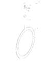
図1に示すように、半導体ウェハめっき用治具10を構成するウェハ保持盤11は、金属めっきを行う電解めっき装置(図示せず)のめっき槽中に浸潤させるために、外周縁に突設している懸架部12の上端に電解めっき装置のめっき槽の上方に吊下するためのホルダー16を設けているA型(以下、ウェハ保持盤11Aという)と、ホルダー16が設けられていないB型(以下、ウェハ保持盤11Bという)との2種類で構成されている。
As shown in FIG. 1, a wafer holder 11 constituting a semiconductor
このウェハ保持盤11A及びウェハ保持盤11Bの相違点は、A型には懸架部12の上端にホルダー16が設けられているところにある。また、ウェハ保持盤11A及びウェハ保持盤11Bの外周縁に突設している懸架部12は、詳細は後述するが、ウェハ保持盤11Aの懸架部12とウェハ保持盤11Bの懸架部12を一体に重ねた場合に、お互いの環状支持板13間が垂直に所定距離(例えば、20mm)の空間を形成するように、懸架部12の中程で外側に屈折するように折り曲げられている。なお、このウェハ保持盤11A及びウェハ保持盤11Bの素材としては、酸に強くさびにくい耐久性に優れた合金であるステンレス鋼(SUS)が好適に用いられる。
The difference between the
図2及び図3に示すように、ウェハ保持盤11A及びウェハ保持盤11Bの本体は、一定幅員の環状支持板13よりなり、図2に示すように環状支持板13の裏面(ウェハ保持盤11Aとウェハ保持盤11Bとを一体に重ねた場合に対抗する面)には環状略中央位置に位置決め部としての凹状溝14を形成しており、この凹状溝14は後述するウェハ圧接盤20の嵌着部としての嵌着凸部21が嵌着する。これにより、ウェハ保持盤11A及びウェハ保持盤11Bとそれぞれのウェハ圧接盤20とにより半導体ウェハ30を容易に位置決めして挟持できるようにしている。
As shown in FIGS. 2 and 3, the main body of the
また、環状支持板13の内周縁部には、環状内空間に接した状態で環状のウェハ保持部としてのウェハ嵌着凹部15を形成しており、このウェハ嵌着凹部15の幅員は半導体ウェハ30の外周縁の略1mmの幅員が載置される大きさとしており、深さは半導体ウェハ30の略同一厚み、すなわち略200μの深さとしている。
Further, a wafer
ウェハ嵌着凹部15には、円盤状の半導体ウェハ30の外周縁部が嵌着して環状内空間を閉塞するように環状支持板13に半導体ウェハ30を支持載置することができるように構成されている。すなわち、環状支持板13の環状内空間に半導体ウェハ30が位置して、電解めっき処理により半導体ウェハ30の裏面に銀及びニッケルがめっき処理される。ここで、本実施形態における半導体ウェハ30のめっき面は、ウェハ保持盤11Aとウェハ保持盤11Bとを一体に重ねた場合に対抗する面ではなく裏側の面である。つまり、半導体ウェハ30は、ウェハ保持盤11Aとウェハ保持盤11Bとを一体に重ねた場合に対抗するように、半導体の実装面(以下、半導体ウェハ30の表面という。)が配置され、それぞれの実装面の裏側の面(以下、半導体ウェハ30の裏面という。)に、電解めっき処理により銀及びニッケル等の金属がめっき処理される。
The
半導体ウェハ30は、例えば、シリコン等の素材が用いられるが、シリコンの表面に銀を直接めっきするのは難しい。そのため、半導体ウェハ30のめっき面(半導体ウェハ30の裏面)には、予め銀の薄い膜が貼付されており、このめっき面に通電することで、銀やニッケルによる電解めっき処理を容易としている。この時、半導体ウェハ30の表面(半導体の実装面)には、回路パターンが形成されており、そこには様々な半導体(例えば、トランジスタやコンデンサ、抵抗等で構成されたIC(半導体集積回路))が実装される。そのため、半導体ウェハ30の表面は、予め絶縁体の素材からなる被膜で覆われており、半導体ウェハ30の表面には銀及びニッケルが電解めっきで付着しないようにしている。
For example, a material such as silicon is used for the
上述した構成により、ウェハ保持盤11A及びウェハ保持盤11Bの環状支持板13の円環域が半導体ウェハ30の裏面の中で電流密度の高い膜厚増大域と一致する為、ウェハ保持盤11A及びウェハ保持盤11Bの一定幅員の環状支持板13上においては銀やニッケルのめっき被膜が集中して膜厚になるものの、半導体ウェハ30の裏面の周縁部は、ウェハ保持盤11A及びウェハ保持盤11Bの環状支持板13で覆われているため膜厚になることなく、その他のめっき域、つまり、ウェハ保持盤11A及びウェハ保持盤11Bの環状支持板13で覆われていない半導体ウェハの裏面(つまり、露出面)では電流分布が均一となり、半導体ウェハ30の裏面における銀やニッケルによるめっきの膜厚を略均一とすることができる。これにより、銀やニッケルのめっきの膜厚を厚くしても均一なめっき処理を可能としている。
With the above-described configuration, the annular area of the
上記構成により、本実施形態においては、従来めっき処理等が行われていない又は、めっき処理が行われていても通電性の向上や抵抗値の低減を図る効果が小さい厚み(例えば、略1〜3μ)の銀のめっきが施されていた半導体ウェハ30の裏面に、膜厚(例えば、略10μ)の銀の電解めっき処理を行うことで、表面に設置される各種半導体集積回路間の導電性の向上や抵抗値の低減を図ることができ、消費電力の低減効果を充分に図ることができる。
With the above-described configuration, in the present embodiment, a thickness with a small effect (for example, approximately 1 to 1) in which conventional plating treatment or the like is not performed, or even if the plating treatment is performed, the effect of improving the conductivity and reducing the resistance value is reduced. Conductivity between various semiconductor integrated circuits installed on the surface of the
図4に示すように、上記したウェハ保持盤11A及びウェハ保持盤11Bの環状支持板13と一体に合体して半導体ウェハ30を挟持するウェハ圧接盤20は、例えば、塩化ビニールの素材で環状板状に形成されている。ウェハ圧接盤20は、環状支持板13の支持板面に略同一の大きさで合わせて圧接可能に構成しており、ウェハ圧接盤20の一面には、ウェハ保持盤11A及びウェハ保持盤11Bと、それぞれの環状支持板13との板面を合わせて合体した場合に、環状支持板13の位置決め部である凹状溝14に嵌着自在となるように、ウェハ圧接盤20の嵌着部である嵌着凸部21をウェハ圧接盤20に突設している。なお、嵌着凸部21は、ウェハ圧接盤20に沿った環条に形成する場合やウェハ圧接盤20の中途を適宜切断した半円弧条とする場合等がある。
As shown in FIG. 4, the wafer
また、上述した実施形態に限らず、位置決め部として凸状突起を環状支持板13に設け、嵌着部として嵌着凹部(凹状溝)をウェハ圧接盤20に設けて、位置決め部としての凸状突起と嵌着部として嵌着凹部を嵌着するように構成することもできる。また、位置決め部として位置決めピンを環状支持板13上に突出して設け、嵌着部として位置決め孔をウェハ圧接盤20に設けて、位置決め部としての位置決めピンを嵌着部として位置決め孔に挿入することで、ウェハ保持盤11A及びウェハ保持盤11Bとウェハ圧接盤20とを位置決めして嵌着するように構成することもできる。すなわち、環状支持板13の位置決め部とウェハ圧接盤20の嵌着部の構成は、環状支持板13とウェハ圧接盤20との間に半導体ウェハ30を確実に位置決めして挟持できる構成であれば、特に限定されるものではない。
Further, not limited to the embodiment described above, a convex protrusion as a positioning portion is provided on the
ウェハ保持盤11A及びウェハ保持盤11Bとウェハ圧接盤20とは上記のように構成されており、両盤を重ねて一体に合体固定するために、複数の圧着治具40を用いる。図5に示すように、圧着治具40は断面U字状の弾性板体(例えば、ポリプロピレン)でクリップ状に形成しており、図1に示すように、90度の間隔で4個の圧着治具40により、ウェハ保持盤11A及びウェハ保持盤11Bの環状支持板13とウェハ圧接盤20との両盤をそれぞれ重ね合わせて外側面から挟持する。このため、圧着治具40には、環状支持板13とウェハ圧接盤20とを挟持するための開口部及びそれに連なる挟持空間41が形成されている。なお、開孔部は先端が狭く形成され、圧着治具40の弾性力で環状支持板13とウェハ圧接盤20とを挟持する構成としている。
The
そして、ウェハ保持盤11Aの懸架部12とウェハ保持盤11Bの懸架部12を一体に重ねて、本実施形態における半導体ウェハめっき用治具10が構成される(図1参照)。これにより、ウェハ保持盤11Aとウェハ保持盤11Bとを構成するそれぞれの環状支持板13間に形成された環状内空間に一枚ずつの半導体ウェハ30が挟持されることになる。すなわち、本実施形態における半導体ウェハめっき用治具10は、一度に二枚の半導体ウェハ30の裏面に電解めっきを同時に行い、膜厚の銀メッキの被膜を形成することができるようにしている。
Then, the semiconductor
半導体ウェハめっき用治具10は上記のように構成されており、以下、かかる治具を用いて半導体ウェハ30の裏面に銀、ニッケルを電解めっきする手順を説明する。
The semiconductor
まず、半導体ウェハめっき用治具10に半導体ウェハ30を取付ける手順を図6〜図11を参照して説明する。図6及び図7に示すように、ウェハ保持盤11A及びウェハ保持盤11Bのそれぞれのウェハ嵌着凹部15にめっき処理対象物となる半導体ウェハ30の外周縁部を嵌着して、ウェハ保持盤11の環状内空間を閉塞する状態に半導体ウェハ30をウェハ保持盤11上に載置する。
First, a procedure for attaching the
次いで、図8に示すように、ウェハ保持盤11A及びウェハ保持盤11Bのそれぞれの環状支持板13上にウェハ圧接盤20を重ねる。この際にウェハ圧接盤20の嵌着凸部21をウェハ保持盤11A及びウェハ保持盤11Bのそれぞれのウェハ嵌着凹部15に嵌着して両盤の位置決め及び合体固定を確実にすると共に、半導体ウェハ30の外周縁部が両盤で挟持固定される。
Next, as shown in FIG. 8, the wafer
そして、図9に示すように、90度の間隔で4個の圧着治具40で、ウェハ保持盤11A及びウェハ保持盤11Bのそれぞれの環状支持板13にウェハ圧接盤20を固定した状態で、ウェハ保持盤11A及びウェハ保持盤11Bのそれぞれの懸架部12を重ねて、半導体ウェハめっき用治具10が構成される。そして、ウェハ保持盤11Aの懸架部12の上端に設けられたホルダー16を、電解めっき装置(図示せず)のめっき槽の上方に吊下して、めっき槽中に半導体ウェハ30を浸漬して電解めっき処理が行われる。すなわち、ホルダー16は、2枚の半導体ウェハ30をウェハ保持盤11A及びウェハ保持盤11Bとそれぞれのウェハ圧接盤20との間に挟持した半導体ウェハめっき用治具10を、めっき処理のために電解めっき装置のめっき槽の上方に吊下するためのものである。
Then, as shown in FIG. 9, with the four pressure bonding jigs 40 at intervals of 90 degrees, the wafer
そして、電解めっき装置のめっき槽中には、銀、ニッケルイオンを含有しためっき液が充填されおり、このめっき液に半導体ウェハ30を浸漬した状態で、半導体ウェハめっき用治具10をカソード(陰極(−))とし、同じくめっき液中に浸漬した銀、ニッケルの金属板をアノード(陽極(+))として外部直流電源から電流を印可する。これにより、アノード側では、アノード反応により電子がカソード側に外部直流電源を通して運ばれて、メッキ槽のめっき液中に銀、ニッケルイオンを放出する。一方、カソード側では、被メッキ面である半導体ウェハ30の裏面に帯電した電子と、めっき槽のめっき液中の銀、ニッケルイオンとのカソード反応により、金属銀、金属ニッケルが析出して半導体ウェハ30の裏面に銀、ニッケルの被膜が形成されてめっき処理が行われる。
The plating tank of the electroplating apparatus is filled with a plating solution containing silver and nickel ions, and the semiconductor
図10及び図11に示すように、ウェハ保持盤11A及びウェハ保持盤11Bの懸架部12の構造は、一定幅員の縦吊下板とその上半部を前方に略45°だけ折曲し、その上端近傍に形成した係合部とよりなり、特に係合部は、前方に突設した合わせ舌片17とよりなる。かかる係合部の構造は2枚の半導体ウェハ30をユニットとして同時に吊下して銀、ニッケルめっき処理するために構成された構造である。すなわち、ウェハ保持盤11A及びウェハ保持盤11Bのそれぞれの環状支持板13を一定間隔の空間を保持して重ね、それぞれに半導体ウェハ30を、ウェハ保持盤11A及びウェハ保持盤11Bの環状支持板13の環状略中央位置に凹状溝14にウェハ圧接盤20の嵌着凸部21を嵌着させて挟持し、それぞれの環状支持板13とウェハ圧接盤20とを位置決めして重ねて圧着治具40で固定する。
As shown in FIGS. 10 and 11, the structure of the
図11に示すように、このようにウェハ保持盤11A及びウェハ保持盤11Bのそれぞれの環状支持板13とウェハ圧接盤20とのユニットを、一定間隔を保持して2ユニット形成し、各ユニットに半導体ウェハ30を挟持させることにより、同時に2枚の半導体ウェハ30を保持してめっき処理することができる。この際に、他方のユニットのウェハ保持盤に突設した懸架部12は一方のユニットの保持盤の懸架部12と対照的な形状に形成し、係合部のみは、ウェハ保持盤11Bに舌片挿通孔18(図3参照)を形成し、この舌片挿通孔18の直上部にウェハ保持盤11Bの受け舌片17を突設し、ウェハ保持盤11Aの合わせ舌片17とウェハ保持盤11Bの受け舌片17とを一体に重ねることで、ウェハ保持盤11A及びウェハ保持盤11Bにそれぞれ挟持された半導体ウェハ30の中心位置を水平に同一とすることができる。なお、一方のユニットのウェハ保持盤11Aの合わせ舌片17とウェハ保持盤11Bの受け舌片17とは略同一形状としている。
As shown in FIG. 11, two units of the
従って、2枚の半導体ウェハ30をユニットとして吊下して同時にめっき処理を行うに際しては半導体ウェハ30を挟持したウェハ保持盤11A及びウェハ保持盤11Bのそれぞれの環状支持板13とウェハ圧接盤20の一方のユニットと同じく他方のユニットとを対向状態に配置し、各ユニットの有する懸架部の係合部を当接して重ねる。この際に、一方の懸架部の合わせ舌片17を他方の懸架部の舌片挿通孔18から突出して受け舌片17と重ねて固定することにより各ユニットは一体に連設されてそれぞれのユニットに挟持された2枚の半導体ウェハ30の裏面に同時に銀、ニッケルめっき処理を行うことができる。
Therefore, when two
次に上述した半導体ウェハめっき用治具10を用いためっき処理方法について図12を参照して説明する。
Next, a plating method using the semiconductor
図12に示すように、まず、2枚の半導体ウェハ30をセットした半導体ウェハめっき用治具10の前処理(ステップS10)を行う。この前処理では、半導体ウェハ30のめっき面(半導体ウェハ30の裏面)を、シアン化カリウム等の溶液に浸漬して不純物の洗浄、表面活性化処理等を行い、以下のめっき工程において、半導体ウェハ30のめっき面への電解めっき処理が均一に行えるようにする。
As shown in FIG. 12, first, pre-processing (step S10) of the semiconductor
次いで、銀めっきを行うめっき槽に半導体ウェハ30を浸漬して所定時間電流を流して銀めっき処理(ステップS11)を行う。この銀めっき処理では、電解めっき装置(図示せず)の銀イオンを含んだめっき液が充填されためっき槽に半導体ウェハ30を浸漬する。このめっき槽では、上述したようにカソード電極として半導体ウェハ30を挟持した半導体ウェハめっき用治具10が用いられ、アソード電極として銀が用いられる。そして、カソード電極を構成する半導体ウェハめっき用治具10とアソード電極を構成する銀とに、図示しない外部直流電源から直流電流が供給されることで、半導体ウェハ30のめっき面(裏面)に銀めっきの被膜が形成される。電解めっきにおいては、この外部直流電源から供給される電流の供給時間及び電流値に応じて所定の厚みの銀めっきの被膜が形成される。このため、本実施形態においては、所定の膜厚(実施形態では略10μ)の銀メッキが形成される電流の供給時間及び電流値が外部直流電源から供給されることになる。
Next, the
このように、半導体ウェハ30のめっき面に従来にない略10μの厚みの銀めっきを形成する場合でも、ウェハ保持盤11A,11Bとそれぞれのウェハ圧接盤20との間に半導体ウェハ30を挟持しているため、特に半導体ウェハ30のめっき面の外周縁部、すなわち環状縁部が、ウェハ保持盤11A及びウェハ保持盤11Bの環状支持板13で覆われた状態で、めっき槽内でめっき液中の銀イオンのカソード反応により、半導体ウェハ30のめっき面の表面に銀めっきの皮膜が形成される。このとき、半導体ウェハ30のめっき面の環状縁部を覆う環状支持板13上においては銀のめっき被膜が集中して膜厚になるものの、その他の環状支持板13で覆われていない半導体ウェハの裏面(つまり、露出面)では電流分布が均一となり、半導体ウェハ30の裏面における銀によるめっきの膜厚を略均一とすることを可能としている。
As described above, even when silver plating having a thickness of about 10 μm, which is not conventionally provided, is formed on the plating surface of the
また、本実施形態においては、半導体ウェハめっき用治具10を構成するウェハ保持盤11Aとウェハ保持盤11Bとに2枚の半導体ウェハ30を挟持する構成としている。そして、2枚の半導体ウェハ30は、ウェハ保持盤11Aとウェハ保持盤11Bの対抗する面に半導体の実装面(非めっき面)が配置され、それぞれの実装面の裏面に半導体ウェハ30のめっき面が配置される構成としている。そして、銀のアノード電極は、カソード電極である半導体ウェハめっき用治具10の外側に所定の距離を置いて2ヶ所配置されることになる。これにより、1箇所のめっき槽において、同時に2枚の半導体ウェハ30のめっき面に銀めっきを行うことを可能としている。
In the present embodiment, two
次いで、半導体ウェハ30のめっき面のシャワー水洗処理(ステップS12)を行う。このシャワー水洗処理では、半導体ウェハ30のめっき面のシャワー洗浄を行い、環状支持板13上やめっき面上の余分なめっき液を洗い流す。
Next, a shower rinsing process (step S12) of the plated surface of the
次いで、半導体ウェハめっき用治具10を所定の浸漬水洗液に漬けて、半導体ウェハ30のめっき面の浸漬水洗処理(ステップS13)を行う。この浸漬水洗処理では、浸漬水洗液に銀めっきした半導体ウェハ30のめっき面を漬けることで、半導体ウェハ30のめっき面上の余分なめっき液を洗浄する。すなわち、本実施形態においては、シャワー水洗処理(ステップS12)及び浸漬水洗処理(ステップS13)の2工程において、半導体ウェハ30のめっき面を洗浄して、めっき面上の余分なめっき液を洗浄している。
Next, the semiconductor
次いで、ニッケルめっきを行うめっき槽に半導体ウェハ30を浸漬して所定時間電流を流してニッケルめっき処理(ステップS14)を行う。このニッケルめっき処理では、電解めっき装置(図示せず)のニッケルイオンを含んだめっき液が充填されためっき槽に半導体ウェハ30を浸漬する。このめっき槽では、上述したようにカソード電極として半導体ウェハ30を挟持した半導体ウェハめっき用治具10が用いられ、アソード電極としてニッケルが用いられる。そして、カソード電極を構成する半導体ウェハめっき用治具10とアソード電極を構成するニッケルとに、図示しない外部直流電源から直流電流が供給されることで、半導体ウェハ30の裏面に施された銀めっきに積層してニッケルめっきが略1μの膜厚で形成される。この場合も、所定の膜厚(実施形態では略1μ)のニッケルめっきが形成される電流の供給時間及び電流値が外部直流電源から供給されることになる。
Next, the
このように、従来にない略10μの銀めっきの上に略1μニッケルめっきを積層した場合でも、環状支持板13上においてはニッケルのめっき被膜が集中して被膜の膜厚が厚くになるものの、その他の環状支持板13で覆われていない半導体ウェハの裏面(つまり、露出面)では電流分布が均一となり、半導体ウェハ30の裏面におけるニッケルによるめっきの膜厚を略均一に保つことを可能としている。
In this way, even when approximately 1 μm nickel plating is laminated on approximately 10 μm silver plating which has not been heretofore, the nickel plating film is concentrated on the
このニッケルめっき処理においても上述した銀めっき処理と同様に、ニッケルのアノード電極は、カソード電極である半導体ウェハめっき用治具10の外側に所定の距離を置いて2ヶ所配置されることになる。これにより、1箇所のめっき槽において、同時に2枚の半導体ウェハ30のめっき面にニッケルめっきを行うことを可能としている。
In this nickel plating process, similarly to the above-described silver plating process, two nickel anode electrodes are arranged at a predetermined distance outside the semiconductor
次いで、半導体ウェハめっき用治具10のシャワー水洗処理(ステップS15)を行う。このシャワー水洗処理では、環状支持板13上や半導体ウェハ30のめっき面のシャワー洗浄を行い、めっき面上の余分なめっき液を洗い流す。
Next, a shower water washing process (step S15) of the semiconductor
次いで、半導体ウェハめっき用治具10を所定の浸漬水洗液に漬けて、半導体ウェハ30のめっき面の浸漬水洗処理(ステップS16)を行う。この浸漬水洗処理では、浸漬水洗液にニッケルめっきした半導体ウェハ30のめっき面を漬けることで、半導体ウェハ30のめっき面上の余分なめっき液を洗浄する。すなわち、本実施形態においては、上述した銀めっき処理の後と同様に、シャワー水洗処理(ステップS15)及び浸漬水洗処理(ステップS16)の2工程において、半導体ウェハ30のめっき面を洗浄して、めっき面上の余分なめっき液を洗浄している。
Next, the semiconductor
次いで、半導体ウェハめっき用治具10に挟持固定された2枚の半導体ウェハ30を取外す。
Next, the two
次いで、取外した2枚の半導体ウェハ30を湯洗浄する湯洗浄処理(ステップS17)を行う。この湯洗浄処理において、上述した工程で、銀とニッケルで電解めっき処理が施された半導体ウェハ30のめっき面を湯洗浄する。このように、半導体ウェハ30のめっき面を湯洗浄することで後述の乾燥処理(ステップS18)におけるメッキ面の乾燥を促進する効果がある。
Next, a hot water cleaning process (step S17) for cleaning the two removed
最後に、2枚の半導体ウェハ30を乾燥する乾燥処理(ステップS18)を行う。この乾燥処理では、銀とニッケルで電解めっき処理した半導体ウェハ30を、定温循環乾燥炉にいれて定温の乾燥した空気にさらすことで、半導体ウェハ30のめっき面を速やかに乾燥させる。この工程を最後として、半導体ウェハ30のめっき処理を終了する。
Finally, a drying process (step S18) for drying the two
上述したように、半導体ウェハ30のめっき面にまず所定膜厚(例えば、10μ)の銀めっきを処理することで、半導体ウェハ30の導電性の向上及び抵抗値の低減を図ることができる。そして、銀めっきの上層に所定膜厚(例えば、1μ)のニッケルめっきを積層することで、銀めっきの拡散を防止するとともに、薬液に対する耐性を高めた半導体ウェハ30のめっき面を形成することができる。
As described above, the plating of the
上述した半導体ウェハのめっき処理方法により製造した半導体ウェハにより製造した半導体装置を有する通信機器、電子機器、映像機器、家電機器、バッテリー等について説明する。 A communication device, an electronic device, a video device, a home appliance, a battery, and the like having a semiconductor device manufactured by the semiconductor wafer manufactured by the above-described semiconductor wafer plating method will be described.
近年では、通信機器として、大型の液晶表示装置を備えたスマートフォンやタブレット型端末等の通信機器が普及している。このような通信機器においては、大型の液晶表示装置を使用しているため消費電力が大きく、従来の携帯電話(所謂、ガラゲー)と比較して機器のバッテリーの消耗が早く頻繁に充電する必要があり、使い勝手が悪いという問題があった。 In recent years, communication devices such as smartphones and tablet terminals equipped with large liquid crystal display devices have become widespread as communication devices. In such a communication device, a large liquid crystal display device is used, so that the power consumption is large, and the battery of the device needs to be charged quickly and frequently as compared with a conventional mobile phone (so-called garage). There was a problem that it was not easy to use.
このような状況において、導電性の高い金属(金、銀、プラチナ、銅等)めっきと、この導電性の高い金属めっきを保護する金属(ニッケル等)めっきとを積層して略均一にめっき処理し、なおかつ、導電性の高い金属めっきの膜厚を可及的に増大した半導体ウェハ30で製造した半導体装置を用いることで、導電性の向上や抵抗値の低下を図ることができ、電気の消耗を抑えた使い勝手の良い通信機器を提供することが可能となる。
In such a situation, a highly conductive metal (gold, silver, platinum, copper, etc.) plating and a metal (nickel, etc.) plating that protects this highly conductive metal plating are laminated almost uniformly. In addition, by using the semiconductor device manufactured by the
また、その他の通信機器、電子機器、映像機器、家電機器、バッテリー等においても、本発明で金属めっきを形成した半導体ウェハ30を用いることで、消費電力の少ない機器を提供することができるため、家庭、会社、公共施設等において省電力を図ることができ、近年問題となっている発電による二酸化炭素の増大を抑えることができ、地球環境にやさしい半導体装置を提供することが可能となる。
In addition, in other communication equipment, electronic equipment, video equipment, home appliances, batteries, etc., by using the
10 半導体ウェハめっき用治具10
11A ウェハ保持盤
11B ウェハ保持盤
12 懸架部
13 環状支持板
14 凹状溝
15 ウェハ嵌着凹部
16 ホルダー
17 舌片
20 ウェハ圧接盤
21 嵌着凸部
30 半導体ウェハ
10 Semiconductor
Claims (11)
ウェハ保持盤は、
外周縁に懸架部を突設した一定幅員の環状支持板と、
環状支持板面に形成した位置決め部と、
環状支持板の内周縁部に形成したウェハ保持部と、により構成し、
ウェハ圧接盤は、
環状支持板の支持板面に圧接する環状板と、
環状支持板の位置決め部に嵌着自在となるように環状板面に形成した嵌着部と、
より構成してなる請求項1に記載の半導体ウェハを製造するための半導体ウェハめっき用治具。 It is composed of a wafer holding disk and a crimping jig that crimps and fixes a wafer pressure welding board separate from the wafer holder so that the semiconductor wafer is sandwiched between them,
The wafer holder is
A fixed-width annular support plate with a suspension projecting from the outer periphery;
A positioning part formed on the annular support plate surface;
A wafer holding part formed on the inner peripheral edge of the annular support plate,
Wafer pressure welding machine
An annular plate in pressure contact with the support plate surface of the annular support plate;
A fitting portion formed on the annular plate surface so as to be freely fitted to the positioning portion of the annular support plate;
A semiconductor wafer plating jig for manufacturing the semiconductor wafer according to claim 1, further comprising:
Priority Applications (1)
| Application Number | Priority Date | Filing Date | Title |
|---|---|---|---|
| JP2016017434A JP6746185B2 (en) | 2016-02-01 | 2016-02-01 | Jig for semiconductor wafer plating |
Applications Claiming Priority (1)
| Application Number | Priority Date | Filing Date | Title |
|---|---|---|---|
| JP2016017434A JP6746185B2 (en) | 2016-02-01 | 2016-02-01 | Jig for semiconductor wafer plating |
Publications (3)
| Publication Number | Publication Date |
|---|---|
| JP2017137523A true JP2017137523A (en) | 2017-08-10 |
| JP2017137523A5 JP2017137523A5 (en) | 2019-03-14 |
| JP6746185B2 JP6746185B2 (en) | 2020-08-26 |
Family
ID=59564851
Family Applications (1)
| Application Number | Title | Priority Date | Filing Date |
|---|---|---|---|
| JP2016017434A Active JP6746185B2 (en) | 2016-02-01 | 2016-02-01 | Jig for semiconductor wafer plating |
Country Status (1)
| Country | Link |
|---|---|
| JP (1) | JP6746185B2 (en) |
Cited By (3)
| Publication number | Priority date | Publication date | Assignee | Title |
|---|---|---|---|---|
| CN110359079A (en) * | 2018-04-10 | 2019-10-22 | 中国科学院半导体研究所 | Electroplating clamp |
| CN112259493A (en) * | 2020-10-19 | 2021-01-22 | 绍兴同芯成集成电路有限公司 | Electroplating and chemical plating integrated process for ultrathin wafer |
| KR102526481B1 (en) * | 2023-01-31 | 2023-04-27 | 하이쎄미코(주) | Cup cell for wafer plating |
Citations (9)
| Publication number | Priority date | Publication date | Assignee | Title |
|---|---|---|---|---|
| JPS647271U (en) * | 1987-06-26 | 1989-01-17 | ||
| JPH07243097A (en) * | 1994-03-07 | 1995-09-19 | Electroplating Eng Of Japan Co | Wafer plating rack and plating method using the rack |
| JPH10303198A (en) * | 1997-04-24 | 1998-11-13 | Mitsubishi Electric Corp | Semiconductor device, manufacture thereof and etchant |
| JP2001247999A (en) * | 2000-03-07 | 2001-09-14 | Ebara Corp | Substrate plating jig |
| JP2006009132A (en) * | 2004-06-29 | 2006-01-12 | Tdk Corp | Cathode electrode assembly, cathode electrode device and plating device |
| JP2007308783A (en) * | 2006-05-22 | 2007-11-29 | Matsushita Electric Ind Co Ltd | Apparatus and method for electroplating |
| JP2010205991A (en) * | 2009-03-04 | 2010-09-16 | Mitsubishi Electric Corp | Semiconductor device and method for manufacturing the same |
| JP2014189806A (en) * | 2013-03-26 | 2014-10-06 | Ebara Corp | Plating apparatus and plating method |
| JP2015145537A (en) * | 2007-12-04 | 2015-08-13 | 株式会社荏原製作所 | Plating apparatus |
-
2016
- 2016-02-01 JP JP2016017434A patent/JP6746185B2/en active Active
Patent Citations (9)
| Publication number | Priority date | Publication date | Assignee | Title |
|---|---|---|---|---|
| JPS647271U (en) * | 1987-06-26 | 1989-01-17 | ||
| JPH07243097A (en) * | 1994-03-07 | 1995-09-19 | Electroplating Eng Of Japan Co | Wafer plating rack and plating method using the rack |
| JPH10303198A (en) * | 1997-04-24 | 1998-11-13 | Mitsubishi Electric Corp | Semiconductor device, manufacture thereof and etchant |
| JP2001247999A (en) * | 2000-03-07 | 2001-09-14 | Ebara Corp | Substrate plating jig |
| JP2006009132A (en) * | 2004-06-29 | 2006-01-12 | Tdk Corp | Cathode electrode assembly, cathode electrode device and plating device |
| JP2007308783A (en) * | 2006-05-22 | 2007-11-29 | Matsushita Electric Ind Co Ltd | Apparatus and method for electroplating |
| JP2015145537A (en) * | 2007-12-04 | 2015-08-13 | 株式会社荏原製作所 | Plating apparatus |
| JP2010205991A (en) * | 2009-03-04 | 2010-09-16 | Mitsubishi Electric Corp | Semiconductor device and method for manufacturing the same |
| JP2014189806A (en) * | 2013-03-26 | 2014-10-06 | Ebara Corp | Plating apparatus and plating method |
Cited By (3)
| Publication number | Priority date | Publication date | Assignee | Title |
|---|---|---|---|---|
| CN110359079A (en) * | 2018-04-10 | 2019-10-22 | 中国科学院半导体研究所 | Electroplating clamp |
| CN112259493A (en) * | 2020-10-19 | 2021-01-22 | 绍兴同芯成集成电路有限公司 | Electroplating and chemical plating integrated process for ultrathin wafer |
| KR102526481B1 (en) * | 2023-01-31 | 2023-04-27 | 하이쎄미코(주) | Cup cell for wafer plating |
Also Published As
| Publication number | Publication date |
|---|---|
| JP6746185B2 (en) | 2020-08-26 |
Similar Documents
| Publication | Publication Date | Title |
|---|---|---|
| US6942780B2 (en) | Method and apparatus for processing a substrate with minimal edge exclusion | |
| JP2005501963A5 (en) | ||
| JP6746185B2 (en) | Jig for semiconductor wafer plating | |
| CN104878435B (en) | Substrate holder, electroplanting device and electro-plating method | |
| KR20050056263A (en) | Plating uniformity control by contact ring shaping | |
| JP5649591B2 (en) | Electroplating holder and electroplating apparatus using the holder | |
| TW201718956A (en) | High resistance virtual anode for electroplating cell, electorplating cell and method of treating surface of substrate | |
| JP4764899B2 (en) | Substrate plating jig, substrate plating equipment | |
| JP2019049046A (en) | Distribution system for chemical and/or electrolytic surface treatment | |
| JP2019049047A (en) | Substrate lock system for chemical and/or electrolytic surface treatment | |
| JP2020132889A (en) | Hanger for plating | |
| JP6815817B2 (en) | Anode unit and plating equipment equipped with the anode unit | |
| US20050274604A1 (en) | Plating apparatus | |
| KR20100077447A (en) | Wafer plating apparatus | |
| TWI570280B (en) | Electroplating cathode fixture and electroplating device for a solar cell | |
| US20070187233A1 (en) | Universal plating fixture | |
| TW200839038A (en) | Device and method with improved plating film thickness uniformity | |
| TWI221862B (en) | Apparatus and method for plating a substrate, and method and apparatus for electrolytic treatment | |
| US20070056856A1 (en) | Apparatus and method for electrically contacting wafer in electronic chemical plating cell | |
| TWM381635U (en) | Electroplate apparatus for plating copper on a printed circuit board | |
| KR100293238B1 (en) | rack for use in substrate plating device | |
| WO2021049145A1 (en) | Substrate holder, substrate plating device equipped therewith, and electrical contact | |
| JP2006016651A (en) | Holder for plating wafer | |
| KR100984074B1 (en) | Apparatus for electroplating to parts with center hole and method for the same | |
| KR100792338B1 (en) | Electric chemical plating cell |
Legal Events
| Date | Code | Title | Description |
|---|---|---|---|
| A521 | Request for written amendment filed |
Free format text: JAPANESE INTERMEDIATE CODE: A523 Effective date: 20190131 |
|
| A621 | Written request for application examination |
Free format text: JAPANESE INTERMEDIATE CODE: A621 Effective date: 20190131 |
|
| A977 | Report on retrieval |
Free format text: JAPANESE INTERMEDIATE CODE: A971007 Effective date: 20191016 |
|
| A131 | Notification of reasons for refusal |
Free format text: JAPANESE INTERMEDIATE CODE: A131 Effective date: 20191112 |
|
| A601 | Written request for extension of time |
Free format text: JAPANESE INTERMEDIATE CODE: A601 Effective date: 20200114 |
|
| A521 | Request for written amendment filed |
Free format text: JAPANESE INTERMEDIATE CODE: A523 Effective date: 20200311 |
|
| TRDD | Decision of grant or rejection written | ||
| A01 | Written decision to grant a patent or to grant a registration (utility model) |
Free format text: JAPANESE INTERMEDIATE CODE: A01 Effective date: 20200707 |
|
| A61 | First payment of annual fees (during grant procedure) |
Free format text: JAPANESE INTERMEDIATE CODE: A61 Effective date: 20200803 |
|
| R150 | Certificate of patent or registration of utility model |
Ref document number: 6746185 Country of ref document: JP Free format text: JAPANESE INTERMEDIATE CODE: R150 |
|
| R250 | Receipt of annual fees |
Free format text: JAPANESE INTERMEDIATE CODE: R250 |