JP2016535937A - Substrate for LED with total internal reflection layer surrounding the LED - Google Patents
Substrate for LED with total internal reflection layer surrounding the LED Download PDFInfo
- Publication number
- JP2016535937A JP2016535937A JP2016528068A JP2016528068A JP2016535937A JP 2016535937 A JP2016535937 A JP 2016535937A JP 2016528068 A JP2016528068 A JP 2016528068A JP 2016528068 A JP2016528068 A JP 2016528068A JP 2016535937 A JP2016535937 A JP 2016535937A
- Authority
- JP
- Japan
- Prior art keywords
- layer
- lens
- led
- refractive index
- substrate surface
- Prior art date
- Legal status (The legal status is an assumption and is not a legal conclusion. Google has not performed a legal analysis and makes no representation as to the accuracy of the status listed.)
- Pending
Links
Images

Classifications
-
- H—ELECTRICITY
- H01—ELECTRIC ELEMENTS
- H01L—SEMICONDUCTOR DEVICES NOT COVERED BY CLASS H10
- H01L33/00—Semiconductor devices with at least one potential-jump barrier or surface barrier specially adapted for light emission; Processes or apparatus specially adapted for the manufacture or treatment thereof or of parts thereof; Details thereof
- H01L33/48—Semiconductor devices with at least one potential-jump barrier or surface barrier specially adapted for light emission; Processes or apparatus specially adapted for the manufacture or treatment thereof or of parts thereof; Details thereof characterised by the semiconductor body packages
- H01L33/58—Optical field-shaping elements
-
- H—ELECTRICITY
- H01—ELECTRIC ELEMENTS
- H01L—SEMICONDUCTOR DEVICES NOT COVERED BY CLASS H10
- H01L33/00—Semiconductor devices with at least one potential-jump barrier or surface barrier specially adapted for light emission; Processes or apparatus specially adapted for the manufacture or treatment thereof or of parts thereof; Details thereof
- H01L33/005—Processes
-
- H—ELECTRICITY
- H01—ELECTRIC ELEMENTS
- H01L—SEMICONDUCTOR DEVICES NOT COVERED BY CLASS H10
- H01L33/00—Semiconductor devices with at least one potential-jump barrier or surface barrier specially adapted for light emission; Processes or apparatus specially adapted for the manufacture or treatment thereof or of parts thereof; Details thereof
- H01L33/48—Semiconductor devices with at least one potential-jump barrier or surface barrier specially adapted for light emission; Processes or apparatus specially adapted for the manufacture or treatment thereof or of parts thereof; Details thereof characterised by the semiconductor body packages
- H01L33/50—Wavelength conversion elements
-
- H—ELECTRICITY
- H01—ELECTRIC ELEMENTS
- H01L—SEMICONDUCTOR DEVICES NOT COVERED BY CLASS H10
- H01L33/00—Semiconductor devices with at least one potential-jump barrier or surface barrier specially adapted for light emission; Processes or apparatus specially adapted for the manufacture or treatment thereof or of parts thereof; Details thereof
- H01L33/48—Semiconductor devices with at least one potential-jump barrier or surface barrier specially adapted for light emission; Processes or apparatus specially adapted for the manufacture or treatment thereof or of parts thereof; Details thereof characterised by the semiconductor body packages
- H01L33/52—Encapsulations
- H01L33/54—Encapsulations having a particular shape
-
- H—ELECTRICITY
- H01—ELECTRIC ELEMENTS
- H01L—SEMICONDUCTOR DEVICES NOT COVERED BY CLASS H10
- H01L33/00—Semiconductor devices with at least one potential-jump barrier or surface barrier specially adapted for light emission; Processes or apparatus specially adapted for the manufacture or treatment thereof or of parts thereof; Details thereof
- H01L33/48—Semiconductor devices with at least one potential-jump barrier or surface barrier specially adapted for light emission; Processes or apparatus specially adapted for the manufacture or treatment thereof or of parts thereof; Details thereof characterised by the semiconductor body packages
- H01L33/52—Encapsulations
- H01L33/56—Materials, e.g. epoxy or silicone resin
-
- H—ELECTRICITY
- H01—ELECTRIC ELEMENTS
- H01L—SEMICONDUCTOR DEVICES NOT COVERED BY CLASS H10
- H01L33/00—Semiconductor devices with at least one potential-jump barrier or surface barrier specially adapted for light emission; Processes or apparatus specially adapted for the manufacture or treatment thereof or of parts thereof; Details thereof
- H01L33/48—Semiconductor devices with at least one potential-jump barrier or surface barrier specially adapted for light emission; Processes or apparatus specially adapted for the manufacture or treatment thereof or of parts thereof; Details thereof characterised by the semiconductor body packages
- H01L33/58—Optical field-shaping elements
- H01L33/60—Reflective elements
-
- H—ELECTRICITY
- H01—ELECTRIC ELEMENTS
- H01L—SEMICONDUCTOR DEVICES NOT COVERED BY CLASS H10
- H01L33/00—Semiconductor devices with at least one potential-jump barrier or surface barrier specially adapted for light emission; Processes or apparatus specially adapted for the manufacture or treatment thereof or of parts thereof; Details thereof
- H01L33/48—Semiconductor devices with at least one potential-jump barrier or surface barrier specially adapted for light emission; Processes or apparatus specially adapted for the manufacture or treatment thereof or of parts thereof; Details thereof characterised by the semiconductor body packages
- H01L33/62—Arrangements for conducting electric current to or from the semiconductor body, e.g. lead-frames, wire-bonds or solder balls
-
- H—ELECTRICITY
- H01—ELECTRIC ELEMENTS
- H01L—SEMICONDUCTOR DEVICES NOT COVERED BY CLASS H10
- H01L2224/00—Indexing scheme for arrangements for connecting or disconnecting semiconductor or solid-state bodies and methods related thereto as covered by H01L24/00
- H01L2224/01—Means for bonding being attached to, or being formed on, the surface to be connected, e.g. chip-to-package, die-attach, "first-level" interconnects; Manufacturing methods related thereto
- H01L2224/10—Bump connectors; Manufacturing methods related thereto
- H01L2224/15—Structure, shape, material or disposition of the bump connectors after the connecting process
- H01L2224/16—Structure, shape, material or disposition of the bump connectors after the connecting process of an individual bump connector
- H01L2224/161—Disposition
- H01L2224/16151—Disposition the bump connector connecting between a semiconductor or solid-state body and an item not being a semiconductor or solid-state body, e.g. chip-to-substrate, chip-to-passive
- H01L2224/16221—Disposition the bump connector connecting between a semiconductor or solid-state body and an item not being a semiconductor or solid-state body, e.g. chip-to-substrate, chip-to-passive the body and the item being stacked
- H01L2224/16225—Disposition the bump connector connecting between a semiconductor or solid-state body and an item not being a semiconductor or solid-state body, e.g. chip-to-substrate, chip-to-passive the body and the item being stacked the item being non-metallic, e.g. insulating substrate with or without metallisation
-
- H—ELECTRICITY
- H01—ELECTRIC ELEMENTS
- H01L—SEMICONDUCTOR DEVICES NOT COVERED BY CLASS H10
- H01L2924/00—Indexing scheme for arrangements or methods for connecting or disconnecting semiconductor or solid-state bodies as covered by H01L24/00
- H01L2924/10—Details of semiconductor or other solid state devices to be connected
- H01L2924/11—Device type
- H01L2924/12—Passive devices, e.g. 2 terminal devices
- H01L2924/1204—Optical Diode
- H01L2924/12041—LED
-
- H—ELECTRICITY
- H01—ELECTRIC ELEMENTS
- H01L—SEMICONDUCTOR DEVICES NOT COVERED BY CLASS H10
- H01L2933/00—Details relating to devices covered by the group H01L33/00 but not provided for in its subgroups
- H01L2933/0008—Processes
- H01L2933/0033—Processes relating to semiconductor body packages
- H01L2933/0058—Processes relating to semiconductor body packages relating to optical field-shaping elements
Landscapes
- Engineering & Computer Science (AREA)
- Microelectronics & Electronic Packaging (AREA)
- Manufacturing & Machinery (AREA)
- Computer Hardware Design (AREA)
- Power Engineering (AREA)
- Led Device Packages (AREA)
Abstract
パッケージされたLEDは、サブストレート表面上にマウントされたLEDダイを含んでいる。低屈折率材料による第1レイヤが、サブストレート表面上で、ダイを取り囲んで形成される。より高い屈折率の材料によるレンズが、LEDダイと第1レイヤの上にモールドされる。レンズと第1レイヤのインターフェイスは、臨界角より大きな角度でLED光が突き当たる場合に、スネルの法則に従って、全内部反射(TIR)によって光を反射する。第1レイヤは、低屈折率のエポキシ、シリコーン、または他の材料であってよい。別の実施例において、LEDダイを取り囲むレイヤは、TIRための空気/レンズのインターフェイスを創成するように、レンズが形成された後で処理される。LEDダイは、蛍光体レイヤを含んでよく、インターフェイスで反射され、サブストレート表面により吸収されない、より多くの側面光を結果として生じる。The packaged LED includes an LED die mounted on the substrate surface. A first layer of low refractive index material is formed surrounding the die on the substrate surface. A lens with a higher refractive index material is molded over the LED die and the first layer. The lens-first layer interface reflects light by total internal reflection (TIR) according to Snell's law when the LED light strikes at an angle greater than the critical angle. The first layer may be a low index epoxy, silicone, or other material. In another embodiment, the layer surrounding the LED die is processed after the lens is formed to create an air / lens interface for TIR. The LED die may include a phosphor layer, resulting in more side light that is reflected at the interface and not absorbed by the substrate surface.
Description
本発明は、サブストレート上にマウントされた発光ダイオード(LED)に関する。特定的には、光取り出し効率を改善するために、LEDを取り囲むサブストレートの反射性を改善する技術に関する。 The present invention relates to a light emitting diode (LED) mounted on a substrate. More specifically, the present invention relates to a technique for improving the reflectivity of a substrate surrounding an LED in order to improve light extraction efficiency.
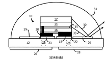
図1は、サブマウント12の上にマウントされた従来のフリップチップLEDダイ10を示している。フリップチップにおいては、nとp両方の電極がLEDダイの底面において形成されている。
FIG. 1 shows a conventional flip chip LED die 10 mounted on a
LEDダイ10は、半導体エピタキシャルレイヤで形成されており、サファイアサブストレートといった、成長サブストレートの上で成長した、nレイヤ14、活性レイヤ15、およびpレイヤ16を含んでいる。図1において成長サブストレートは、レーザリフトオフ(lift−off)、エッチング(ething)、グライディング(grinding)、または他の技術によって、取り除かれている。一つの実施例において、エピタキシャルレイヤは、GaNベースであり、そして、活性レイヤ15は青色光を発する。
The LED die 10 is formed of a semiconductor epitaxial layer and includes an
作成済み(pre−fabricated)の蛍光体タイル17が、LEDダイ10の上面にわたり、シリコーンまたは他の透明な接着剤(図示なし)によって貼り付けられている。白色光のために、タイル17は、YAG蛍光体で形成されてよく、黄色光を発する。青色LED光のいくらかは、タイル17を通じて漏れ、そして、黄色光と混合する。より温かい白色を作成するために、赤色蛍光体レイヤが追加されてよい。
A
金属電極18は、pレイヤ16と電気的に接触しており、そして、金属電極20は、nレイヤ14と電気的に接触している。一つの実施例において、電極18と20は、金パッド(gold pad)であり、セラミック製サブマウント12上でアノードおよびカソード金属パッド22と23に対して超音波溶接(ultrsonically welded)されている。サブマウント12は、プリント回路基板への接合のために、底面金属パッド26と28に至る導電性(conductive)ビア(via)を有している。
米国特許第8536608号は、現在の譲受人に対して譲渡され、ここにおいて参照により包含されているが、サブマウント12の表面に貼り付けられ、かつ、LEDダイ10を取り囲んでいる反射性リング(例えば、R>90%)の使用を説明している。リング29は、スパッタされたアルミニウム(Al)または銀(Ag)レイヤといった、反射性材料で形成されている。リング29は、蛍光体タイル17と活性レイヤ15によって下向きに生成された光を反射する(例えば、光線32と33)。サブマウントは、典型的には、セラミック、ケイ素、または、他の光吸収材料であり、そうして、リング29は、効率を増すように、パッケージによる光の吸収を低減する。
U.S. Pat. No. 8,536,608 is assigned to the current assignee and is hereby incorporated by reference, but is attached to the surface of the
LEDダイ10、蛍光体タイル17、およびリング29は、次に、モールドされた、透明な半球レンズ34によってカプセル化(encapsulate)される。シリコーンで形成されたといったものであり、LEDダイ10を保護し、かつ、光取り出し効率を増加させる。レンズ34の屈折率(例えば、n=1.5)は、典型的には、空気の屈折率と種々のLEDレイヤの屈折率との間である。
The LED die 10,
リング29の反射性が比較的に高いとはいえ、それは100%ではない。従って、リング29によるいくらかの光吸収が未だに存在している。さらに、リング29材料の外エッジ(outer edge)は、レンズ34のエッジの以前に終了する必要がある。レンズ34とサブマウント面との間の良好な気密(hermetic seal)を確保するためである。従って、リング29のエッジとレンズ34のエッジとの間で、いくらかの光の散乱および吸収が存在している。さらに、金属リングを形成することは、比較的に複雑であり、かつ、パッケージについてコストを追加する。
Although the reflectivity of the
必要なものは、LEDダイおよび蛍光体タイルからのより下向きの光さえ反射するための技術である。 What is needed is a technique for reflecting even the downward light from LED dies and phosphor tiles.
サブストレート上にマウントされたLEDダイを取り囲んでいる反射性材料からなるリングの代わりに、全内部反射(TIR)を使用する絶縁性リングが使用される。TIRを用いると、反射は100%である。 Instead of a ring of reflective material surrounding the LED die mounted on the substrate, an insulating ring using total internal reflection (TIR) is used. With TIR, the reflection is 100%.
一つの実施例においては、絶縁材料の滑らかで、薄いレイヤがサブストレート表面上で、かつ、LEDダイの周りに形成される。その材料は、カプセル化しているレンズ材料の屈折率(例えば、n=1.5)より小さい屈折率(例えば、n<1.4)を有している。材料は、サブストレート表面およびレンズ材料に対して非常に良好な付着性を有している。材料は、防湿(moisture proof)であり、レンズのエッジを越えて拡がってよい。 In one embodiment, a smooth and thin layer of insulating material is formed on the substrate surface and around the LED die. The material has a refractive index (eg, n <1.4) that is less than the refractive index of the encapsulating lens material (eg, n = 1.5). The material has very good adhesion to the substrate surface and lens material. The material is moisture proof and may extend beyond the edge of the lens.
臨界角(critical angle)より大きい角度でレンズと低屈折率材料とのインターフェイス上に突き当たっているあらゆる蛍光体またはLEDの光は、実質的に100%の反射率でインターフェイスで反射する。低屈折率材料は、反射性金属よりも、デポジットするのが簡素である。低屈折率材料は、レンズのエッジを越えて拡がり得るので、あらゆるエッジにおいて光の散乱は存在せず、そして、最大量の光が反射される。さらに、材料は絶縁性であり、ミスアライメント(misalignment)による電極の短絡(short)に関する問題は存在しない。 Any phosphor or LED light impinging on the lens / low index material interface at an angle greater than the critical angle will reflect at the interface with substantially 100% reflectivity. Low refractive index materials are easier to deposit than reflective metals. Since the low index material can extend beyond the edge of the lens, there is no light scattering at any edge and the maximum amount of light is reflected. In addition, the material is insulative and there is no problem with electrode shorts due to misalignment.
低屈折率材料自身が、また、拡散白色レイヤ(diffusing white layer)といった、反射性である場合、臨界角より小さい角度で突き当たっているあらゆる光は、TIR以外によって反射されて、サブストレートによって吸収されない。そうした白色レイヤは、TiO2パーティクルを含んでいる低屈折率のエポキシであってよい。 If the low index material itself is also reflective, such as a diffusing white layer, any light impinging at an angle less than the critical angle will be reflected outside the TIR and not absorbed by the substrate. . Such a white layer may be a low refractive index epoxy containing TiO 2 particles.
別の実施例においては、密封された空気のレイヤ(n=1)が、サブストレート表面上で、かつ、LEDダイの周りに形成される。最大のTIRと最小の臨界角を達成するためである。空気のレイヤは、LEDダイ領域の周りに刻み目を有するようにサブストレートをモールドすることによって形成され得る。レンズをモールドする以前に、刻み目は材料で満たされており、材料はレンズ材料が刻み目の中に満たされることを初期的に防いでいる。レンズが形成された後で、材料は、エアーギャップを創成するために蒸発、溶解、または収縮される。空気/レンズのインターフェイスは、優秀なTIRインターフェイスを形成する。 In another embodiment, a sealed layer of air (n = 1) is formed on the substrate surface and around the LED die. This is to achieve the maximum TIR and the minimum critical angle. The air layer may be formed by molding the substrate to have a score around the LED die area. Prior to molding the lens, the indentation is filled with material, which initially prevents the lens material from filling into the indentation. After the lens is formed, the material is evaporated, dissolved, or shrunk to create an air gap. The air / lens interface forms an excellent TIR interface.
別の実施例において、エアーギャップは、大部分が空気である多孔性の絶縁材料によって形成される。 In another embodiment, the air gap is formed by a porous insulating material that is mostly air.
別の実施例においては、親水性タイプ(hydrophilic−type)の材料が、刻まれたリング(堀(moat))の中といった、LEDダイの周りにデポジットされる。それにより、モールドされたレンズ材料は、親水性タイプの材料には付着しないが、そのマッピングラインのサブストレート表面に対して付着する。レンズが形成された後で、親水性タイプの材料は、次に、熱または紫外線(UV)光を用いてキュアされて、レンズから離れて収縮する。このことは、残っている親水性タイプの材料とレンズとの間に非常に薄いエアーギャップを結果として生じ、TIRインターフェイスを創成する。一つの適切な親水性タイプの材料は、油(oil)である。 In another embodiment, a hydrophilic-type material is deposited around the LED die, such as in an engraved ring (moat). Thereby, the molded lens material does not adhere to the hydrophilic type material but adheres to the substrate surface of the mapping line. After the lens is formed, the hydrophilic type material is then cured using heat or ultraviolet (UV) light to shrink away from the lens. This results in a very thin air gap between the remaining hydrophilic type material and the lens, creating a TIR interface. One suitable hydrophilic type material is oil.
本発明は、フリップチップLED(両方の電極が底面にある)、垂直方向LED(一つの電極が上面にあり一つの電極が底面にある)、および横方向LED(両方の電極が上面にある)を含む、あらゆるタイプのLEDダイのパッケージに対して適用される。本発明は、また、蛍光体変換LED(pc−LED)および非pc−LEDにも適用される。pc−LEDについて、蛍光体は、タイルとしてLEDダイの上面に貼り付けられ、または、LEDダイの上面と側面をカバーしてよい。pc−LEDを用いると、本発明を使用することによって、より多くの側面光と、従って、より多くの効率向上が存在する。 The present invention includes flip chip LEDs (both electrodes on the bottom), vertical LEDs (one electrode on the top and one electrode on the bottom), and lateral LEDs (both electrodes on the top). It applies to all types of LED die packages, including The invention also applies to phosphor converted LEDs (pc-LEDs) and non-pc-LEDs. For pc-LEDs, the phosphor may be affixed to the top surface of the LED die as a tile or may cover the top and side surfaces of the LED die. With pc-LEDs, there is more side light and thus more efficiency gains by using the present invention.
サブストレートは、LEDダイとプリント回路基板との間のインターポーザ(interposer)として使用されるサブマウントであってよい。 The substrate may be a submount used as an interposer between the LED die and the printed circuit board.
種々の図面において同一または類似のエレメントは、同一の数字を用いてラベル付けされる。 In the various figures, the same or similar elements are labeled with the same numbers.
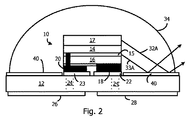
図2は、金属製反射性リングが、シリコーンレンズ34の屈折率より低い屈折率を有する絶縁レイヤ40に置き換えられたことを除いて、図1に類似した、パッケージされたLEDモジュールを示している。レンズ34の屈折率が1.5−1.6であると仮定すると、レイヤ40は、望ましくは、1.4より小さい屈折率を有する。しかしながら、レンズ材料よりも小さいあらゆる屈折率が、インターフェイスにおけるTIRを創成するであろう。屈折率の違いは、臨界角(critical angle)を決定する。望ましい実施例において、屈折率の違いは、少なくとも0.4である。レイヤ40は、エポキシ、シリコーン、または、他の適切な材料によって形成されてよい。そうしたエポキシおよびシリコーンは、商業的に利用可能であり、下に1.38までの屈折率を選択することができる。例えば、メチルベース(methyl−based)のシリコーンは、屈折率が1.4である。そうした材料は、防湿(moisture proof)であり、かつ、レンズ材料とサブストレート表面に上手く付着するので、レイヤ40は、LEDダイ10の周りのサブストレート12の表面全体にわたりデポジット(deposit)されてよく、そして、レンズ34が、レイヤ40の上に直接的にモールドされてよい。従って、エッジ効果は存在せず、そいて、最大の反射性領域が存在する。
FIG. 2 shows a packaged LED module similar to FIG. 1 except that the metallic reflective ring has been replaced with an insulating
レイヤ40は、LEDダイ領域の上にマスクを使用して、LED10ダイの取り付け以前にサブストレート12に対してデポジットされてよい。代替的に、「リフトオフ」レイヤが、LEDダイ10の上にデポジットされてよく、レイヤ40のブランケットデポジション(blanket deposition)が後に続く。リフトオフ材料は、次に、溶解され(dissolved)、そして、LEDダイ10の上のレイヤ40部分が取り外される。
The
レイヤ40とレンズ34との間のインターフェイスだけがTIRについて関係するので、レイヤ40はあらゆる厚さであってよい。例えば、レイヤ40は、3ミクロンより薄くてよい。インターフェイスは、最大のTIRのために、できる限り平滑であるべきである。
Since only the interface between
図2は、吸収がなくTIRを使用してインターフェイスに反射している光線32Aと33Aを図示している。蛍光体タイル17と活性レイヤ15からの下向き光の圧倒的多数がレイヤ40に関して浅い角度であるので、入射光は臨界角より大きな角度で突き当り、そして、スネルの法則(Snell’s Law)に従ってTIRにより反射される。サブストレートの金属パッド22と23は、反射性であってよく(例えば、AlまたはAg)、そして、LEDダイ10の下から外へ延びてよい。臨界角より小さな角度において光を反射するためである。レイヤ40は、LED10の下から外に延びるパッド22と23のあらゆる部分の上に形成されてよい。
FIG. 2 illustrates
LED10は、残りの構造体に関して、かなり、実際のデバイスにおけるよりも、より厚く、かつ、より広く示されている。実際のデバイスにおいて、LEDダイ10は、たった10ミクロンより低い高さであってよく、そして、その幅は0,5mmより小さくてよい。半球レンズ34は、約5mmの直径であってよい。
The
パッケージから外へ反射される光の量を増加させる目的を達成するために、レイヤ40について蛍光体の使用は必要とされない。蛍光体タイル17(または、他のタイプの蛍光体レイヤ)がより厚ければ、より多くの側面光(side light)が生成され、かつ、レイヤ40によって反射される。
In order to achieve the purpose of increasing the amount of light reflected out of the package, the use of a phosphor for
LEDダイ10は、フリップチップとして示されているが、LEDダイは、代わりに、垂直方向または横方向のLEDであってよく、サブストレート上の金属パッドに接続されている一つまたはそれ以上のワイヤーボンド(wire bond)を伴っている。ワイヤーはレンズ34によってカプセル化されている。LEDダイのフットプリントを越えて拡がる金属パッド(例えば、ワイヤーボンドパッド)が存在する場合、レイヤ40は、ワイヤーボンディングが行われた後で、これらのパッドの上にデポジットされてよい。
Although the LED die 10 is shown as a flip chip, the LED die may instead be a vertical or lateral LED and one or more connected to a metal pad on the substrate. It is accompanied by a wire bond. The wire is encapsulated by a
別の実施例において、レイヤ40は、図1に示されるように、反射性金属リング29の上に形成されてもよい。レイヤ40を通過する臨界角より小さい角度におけるあらゆる光がリング29によって反射されるようにである。
In another embodiment, the
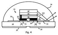
図3と図4は、パッケージされたLEDモジュールを示しており、LEDダイ10を取り囲む低屈折率レイヤは空気である。 3 and 4 show the packaged LED module, where the low refractive index layer surrounding the LED die 10 is air.
図3において、サブストレート12は、LEDダイ10の周りに円形の堀44(刻み目)を含むようにモールドされる。堀は、レンズ34のエッジの前で終了している。堀44は、平坦な上面を有する材料で満たされており、レンズ34がその上にモールドされるときに、滑らかなインターフェイス表面を提供する。材料は、レンズ材料から蒸発、溶解、収縮するタイプのものであり、もしくは、キュアリング(curing)の後で多孔性になるものである。材料を蒸発させるために、レーザアブレーション(laser ablation)も、また、使用されてよい。サブストレート12の上にレンズ34がモールドされた後で、堀44の中の材料がキュアされる。材料が、レンズ34から離れて、蒸発、溶解、収縮し、もしくは、多孔性である場合に、堀44は、空気46または別の低屈折率ガスを用いて主として満たされる。空気/レンズのインターフェイスは、そして、屈折率において最大の差異を有し、幅広い範囲の光角度にわたりTIRを提供する。堀44を使用することによって、平坦な表面を有する材料の正確な量が提供され得る。光線32Bと33Bは、空気/レンズのインターフェイスで反射しているものと示されている。
In FIG. 3, the
一つの実施例において、堀44はゾルゲル(sol−gel)で満たされている。ゾルゲルは、よく知られており、そして、ゲルを形成するための溶媒の中にナノパーティクル(nano−particle)を含んでいる。レンズ34が形成された後で、溶媒は熱によって乾燥され、いくらかの収縮とナノパーティクルによって形成された結晶(crystal)を結果として生じている。結果としてレイヤは、レンズ34の下にエアーギャップ(air gap)を創成する。
In one embodiment, the
エアーギャップは、また、図1の反射性金属リング29の上にも創成されてよく、エアーギャップを貫通しているあらゆる光線がリング29によって反射される。
An air gap may also be created on the
図4は、図3に類似しているが、油(oil)といった、親水性タイプ(hydrophilic−type)の材料を、形成されるべきエアーギャップを伴う領域においてデポジットすることによって形成される。そうした親水性タイプの材料は、シリコーンまたは他のレンズ材料への付着を妨げることが知られている。レンズが形成された後で、レンズ34はサブストレート12の表面に接着されるが、親水性タイプの材料には付着しない。親水性タイプの材料は、次に、収縮するように熱せられ、または、そうでなければキュアされて、図4に示されるエアーギャップを残している。別の実施例において、親水性タイプの材料は、図3における堀44を満たしてよく、そして、キュアリングの最中に収縮するとき、親水性タイプの材料がレンズ34から引き離し、エアーギャップを創成している。光線32Cと33Cは、空気/レンズのインターフェイスで反射しているものと示されている。
FIG. 4 is similar to FIG. 3, but is formed by depositing a hydrophilic-type material, such as an oil, in an area with an air gap to be formed. Such hydrophilic types of materials are known to prevent adhesion to silicone or other lens materials. After the lens is formed, the
処理(processing)が、多くのLEDダイを支持しているサブストレートウェファの上で実行される場合、サブストレート12は、次に、個々のLED/サブストレートを形成するために単一化される。ここでは、種々の図が個別のLED/サブストレートを表わすことができる。
If processing is performed on a substrate wafer supporting many LED dies, the
サブストレート12は、実施例において、LEDダイとプリント回路基板(PCB)との間のサブマウントインターポーザ(interposer)であるが、PCBといった、あらゆるサブストレートが使用されてよい。
The
本発明の所定の実施例が示され、説明されてきたが、当業者にとっては、変更および変形が、本発明の範囲から逸脱することなく、より広い態様においてなされ得ること、かつ、従って、添付の特許請求の範囲は、全てのそうした変更および変形を本発明の真の主旨および範囲内にあるものとして包含するものであることが、明らかであろう。 While certain embodiments of the present invention have been shown and described, it will be apparent to those skilled in the art that changes and modifications can be made in a broader aspect without departing from the scope of the invention, and thus It will be apparent that the following claims are intended to cover all such modifications and variations as fall within the true spirit and scope of the invention.
Claims (15)
サブストレート表面上にマウントされた発光ダイオード(LED)ダイと、
LEDダイをカプセル化し、かつ、前記サブストレート表面上に拡がっている第1材料からなるレンズであり、前記第1材料は第1屈折率を有する、レンズと、
前記LEDダイを取り囲む前記サブストレート表面上の第2材料からなる第1レイヤであり、前記第2材料と前記第1材料は、前記LEDダイを取り囲むインターフェイスにおいて接触し、前記第2材料は前記第1屈折率より小さい第2屈折率を有する、第1レイヤと、
を含む、デバイス。 A light emitting device,
A light emitting diode (LED) die mounted on the substrate surface;
A lens made of a first material encapsulating an LED die and spreading on the surface of the substrate, wherein the first material has a first refractive index;
A first layer of a second material on the substrate surface surrounding the LED die, wherein the second material and the first material contact at an interface surrounding the LED die, and the second material is the first material A first layer having a second refractive index less than one refractive index;
Including the device.
請求項1に記載のデバイス。 The first material includes silicone molded on the substrate surface;
The device of claim 1.
請求項2に記載のデバイス。 The silicone has a refractive index greater than 1.5;
The device of claim 2.
請求項1に記載のデバイス。 The first layer of the second material extends below the outer edge of the lens;
The device of claim 1.
請求項1に記載のデバイス。 The periphery of the first layer with the second material is inside the lens,
The device of claim 1.
請求項1に記載のデバイス。 The first layer of the second material includes a layer of gas;
The device of claim 1.
請求項6に記載のデバイス。 The gas includes air,
The device of claim 6.
請求項1に記載のデバイス。 The first layer of the second material comprises one of silicone or epoxy;
The device of claim 1.
請求項1に記載のデバイス。 The difference between the first refractive index and the second refractive index is at least 0.4;
The device of claim 1.
前記サブストレート表面上に形成された収縮可能な第2レイヤであり、前記第2材料を含んでいるギャップを創成するように前記レンズからの引き戻しを有する、第2レイヤ、を含み、
前記第2材料はガスを含む、
請求項1に記載のデバイス。 The device further comprises:
A shrinkable second layer formed on the substrate surface, the second layer having a pull back from the lens to create a gap containing the second material;
The second material includes a gas;
The device of claim 1.
前記サブストレート表面上に形成された多孔性レイヤ、を含み、
前記多孔性レイヤは、前記第2材料を含み、
前記第2材料は、ガスを含む、
請求項1に記載のデバイス。 The device further comprises:
A porous layer formed on the substrate surface,
The porous layer comprises the second material;
The second material includes a gas;
The device of claim 1.
請求項1に記載のデバイス。 The substrate surface is a submount surface;
The device of claim 1.
前記蛍光体レイヤから発せられた光の少なくとも一部分は、全内部反射(TIR)によって前記インターフェイスで反射する、
請求項1に記載のデバイス。 The LED die includes a phosphor layer;
At least a portion of the light emitted from the phosphor layer is reflected at the interface by total internal reflection (TIR);
The device of claim 1.
前記刻み目のうち少なくとも一部は、前記第2材料を含む、
請求項1に記載のデバイス。 The substrate surface has a notch surrounding the LED die;
At least a portion of the indentation includes the second material,
The device of claim 1.
サブストレート表面上にマウントされた発光ダイオード(LED)ダイを提供するステップと、
前記サブストレート表面上に第1材料による第1レイヤを形成するステップと、
前記LEDダイの上で、かつ、前記第1レイヤの上に、第2材料によるレンズを形成するステップであり、前記第2材料は、屈折率を有している、ステップと、
前記サブストレート表面と前記第2材料との間にガスを含んでいるギャップを生じさせるように、前記レンズが形成された後で前記第1レイヤを処理するステップであり、前記ガスが前記第2材料と接触するインターフェイスが創生され、前記ガスの屈折率は第2材料の屈折率より小さい、ステップと、
を含む、方法。 A method of forming a light emitting device comprising:
Providing a light emitting diode (LED) die mounted on a substrate surface;
Forming a first layer of a first material on the substrate surface;
Forming a lens of a second material on the LED die and on the first layer, the second material having a refractive index; and
Processing the first layer after the lens is formed to create a gas-containing gap between the substrate surface and the second material, wherein the gas is the second material. An interface is created in contact with the material, and the refractive index of the gas is less than the refractive index of the second material;
Including the method.
Applications Claiming Priority (5)
| Application Number | Priority Date | Filing Date | Title |
|---|---|---|---|
| US201361901072P | 2013-11-07 | 2013-11-07 | |
| US61/901,072 | 2013-11-07 | ||
| US201461935360P | 2014-02-04 | 2014-02-04 | |
| US61/935,360 | 2014-02-04 | ||
| PCT/IB2014/065525 WO2015068072A1 (en) | 2013-11-07 | 2014-10-22 | Substrate for led with total-internal reflection layer surrounding led |
Related Child Applications (1)
| Application Number | Title | Priority Date | Filing Date |
|---|---|---|---|
| JP2019237633A Division JP2020061574A (en) | 2013-11-07 | 2019-12-27 | Substrate for led with total inner reflection layer surrounding led |
Publications (2)
| Publication Number | Publication Date |
|---|---|
| JP2016535937A true JP2016535937A (en) | 2016-11-17 |
| JP2016535937A5 JP2016535937A5 (en) | 2017-11-30 |
Family
ID=51999464
Family Applications (2)
| Application Number | Title | Priority Date | Filing Date |
|---|---|---|---|
| JP2016528068A Pending JP2016535937A (en) | 2013-11-07 | 2014-10-22 | Substrate for LED with total internal reflection layer surrounding the LED |
| JP2019237633A Pending JP2020061574A (en) | 2013-11-07 | 2019-12-27 | Substrate for led with total inner reflection layer surrounding led |
Family Applications After (1)
| Application Number | Title | Priority Date | Filing Date |
|---|---|---|---|
| JP2019237633A Pending JP2020061574A (en) | 2013-11-07 | 2019-12-27 | Substrate for led with total inner reflection layer surrounding led |
Country Status (7)
| Country | Link |
|---|---|
| US (1) | US9899579B2 (en) |
| EP (1) | EP3066698B1 (en) |
| JP (2) | JP2016535937A (en) |
| KR (1) | KR102304741B1 (en) |
| CN (1) | CN105684174B (en) |
| TW (2) | TWI621287B (en) |
| WO (1) | WO2015068072A1 (en) |
Cited By (1)
| Publication number | Priority date | Publication date | Assignee | Title |
|---|---|---|---|---|
| JP2018092974A (en) * | 2016-11-30 | 2018-06-14 | 日亜化学工業株式会社 | Package and method of manufacturing package, and light-emitting device and method of manufacturing light-emitting device |
Families Citing this family (10)
| Publication number | Priority date | Publication date | Assignee | Title |
|---|---|---|---|---|
| US9508907B2 (en) * | 2014-09-15 | 2016-11-29 | Koninklijke Philips N.V. | Light emitting device on a mount with a reflective layer |
| CN107689408B (en) * | 2016-08-04 | 2020-03-17 | 展晶科技(深圳)有限公司 | Light emitting diode flip chip die and display |
| KR20180046274A (en) * | 2016-10-27 | 2018-05-08 | 엘지이노텍 주식회사 | Semiconductor device package |
| CN111293199A (en) * | 2017-01-20 | 2020-06-16 | 光宝光电(常州)有限公司 | Light emitting diode packaging structure and light emitting diode packaging module |
| US10020426B1 (en) * | 2017-04-10 | 2018-07-10 | Advanced Optoelectronic Technology, Inc | Light emitting device |
| KR102454083B1 (en) * | 2017-08-30 | 2022-10-12 | 엘지디스플레이 주식회사 | Micro-LED display device and method of fabricating the same |
| CN109638137A (en) * | 2018-11-07 | 2019-04-16 | 惠州市华星光电技术有限公司 | Flip LED chips and down straight aphototropism mode set |
| US20220190213A1 (en) * | 2020-12-15 | 2022-06-16 | Lumileds Llc | Material stack for leds with a dome |
| KR20230045840A (en) | 2021-09-29 | 2023-04-05 | 엘지디스플레이 주식회사 | Display device |
| CN116344723B (en) * | 2023-05-31 | 2023-08-29 | 硅能光电半导体(广州)有限公司 | Batwing light type LED lamp bead structure and preparation method thereof |
Citations (22)
| Publication number | Priority date | Publication date | Assignee | Title |
|---|---|---|---|---|
| JPH08162574A (en) * | 1994-12-05 | 1996-06-21 | Sanken Electric Co Ltd | Circuit device provided with semiconductor element |
| JP2002261333A (en) * | 2001-03-05 | 2002-09-13 | Toyoda Gosei Co Ltd | Light-emitting device |
| JP2003046143A (en) * | 2000-09-29 | 2003-02-14 | Omron Corp | Optical device for optical element and apparatus using the same |
| JP2005223112A (en) * | 2004-02-05 | 2005-08-18 | Citizen Electronics Co Ltd | Surface mounting light emitting diode |
| WO2006104061A1 (en) * | 2005-03-29 | 2006-10-05 | Kyocera Corporation | Reflective member, light-emitting device using same and illuminating device |
| JP2007201392A (en) * | 2005-04-27 | 2007-08-09 | Kyocera Corp | Light emitting element mounting substrate and light emitting device using the same |
| WO2007114306A1 (en) * | 2006-03-29 | 2007-10-11 | Kyocera Corporation | Light emitting device |
| JP2008230866A (en) * | 2007-03-16 | 2008-10-02 | Daicel Chem Ind Ltd | Void forming agent and porous formed body |
| JP2009182085A (en) * | 2008-01-30 | 2009-08-13 | Kyocera Corp | Light emitting device |
| JP2009535798A (en) * | 2006-04-25 | 2009-10-01 | コーニンクレッカ フィリップス エレクトロニクス エヌ ヴィ | Embedded LED |
| WO2009121314A1 (en) * | 2008-03-31 | 2009-10-08 | Osram Opto Semiconductors Gmbh | Radiation-emitting semi-conductor component and method for producing a radiation-emitting semi-conductor component |
| US20100006877A1 (en) * | 2008-07-09 | 2010-01-14 | Himax Display, Inc. | Light-emitting diode package |
| JP2010517213A (en) * | 2007-01-19 | 2010-05-20 | コーニンクレッカ フィリップス エレクトロニクス エヌ ヴィ | Light emitting device with improved heat transfer |
| JP2010517069A (en) * | 2007-01-19 | 2010-05-20 | コーニンクレッカ フィリップス エレクトロニクス エヌ ヴィ | Optical element having at least one embedded reflector |
| US20110001148A1 (en) * | 2009-07-06 | 2011-01-06 | Zhuo Sun | Thin flat solid state light source module |
| JP2011009297A (en) * | 2009-06-23 | 2011-01-13 | Kyocera Corp | Light-emitting device and lighting device |
| US20110062470A1 (en) * | 2009-09-17 | 2011-03-17 | Koninklijke Philips Electronics N.V. | Reduced angular emission cone illumination leds |
| JP2011066302A (en) * | 2009-09-18 | 2011-03-31 | Showa Denko Kk | Semiconductor light emitting device, and method of manufacturing the same |
| JP2011076691A (en) * | 2009-10-01 | 2011-04-14 | Mitsubishi Kagaku Media Co Ltd | Optical recording medium |
| WO2012141094A1 (en) * | 2011-04-13 | 2012-10-18 | シャープ株式会社 | Light source module, and electronic apparatus provided with same |
| JP2012533182A (en) * | 2009-07-15 | 2012-12-20 | オスラム オプト セミコンダクターズ ゲゼルシャフト ミット ベシュレンクテル ハフツング | Light emitting diode and method for manufacturing light emitting diode |
| JP2013077798A (en) * | 2011-09-14 | 2013-04-25 | Toyoda Gosei Co Ltd | Glass sealing led lamp and manufacturing method of the same |
Family Cites Families (16)
| Publication number | Priority date | Publication date | Assignee | Title |
|---|---|---|---|---|
| JP4125848B2 (en) * | 1999-12-17 | 2008-07-30 | ローム株式会社 | Chip type light emitting device with case |
| US6578989B2 (en) * | 2000-09-29 | 2003-06-17 | Omron Corporation | Optical device for an optical element and apparatus employing the device |
| KR100436302B1 (en) * | 2000-09-29 | 2004-07-02 | 오므론 가부시키가이샤 | Optical Device for an Optical Element and Apparatus Employing the Device |
| TWI233220B (en) | 2004-06-18 | 2005-05-21 | Chi Mei Optoelectronics Corp | Light emitting diode package |
| US7378686B2 (en) * | 2005-10-18 | 2008-05-27 | Goldeneye, Inc. | Light emitting diode and side emitting lens |
| RU2302687C1 (en) | 2006-02-26 | 2007-07-10 | Закрытое акционерное общество "ПОЛА+" | Light-emitting diode device |
| US7889421B2 (en) * | 2006-11-17 | 2011-02-15 | Rensselaer Polytechnic Institute | High-power white LEDs and manufacturing method thereof |
| JP2009289816A (en) | 2008-05-27 | 2009-12-10 | Kyocera Corp | Light emitting device, and lighting system |
| JP5689225B2 (en) * | 2009-03-31 | 2015-03-25 | 日亜化学工業株式会社 | Light emitting device |
| US8168998B2 (en) | 2009-06-09 | 2012-05-01 | Koninklijke Philips Electronics N.V. | LED with remote phosphor layer and reflective submount |
| KR20110121176A (en) * | 2010-04-30 | 2011-11-07 | 삼성엘이디 주식회사 | Semiconductor light emitting device and preparing therof |
| JP4962635B1 (en) * | 2011-03-15 | 2012-06-27 | オムロン株式会社 | Optical semiconductor package, optical semiconductor module, and manufacturing method thereof |
| JP5449274B2 (en) | 2011-03-25 | 2014-03-19 | シャープ株式会社 | Lighting device and display device |
| JP5401534B2 (en) * | 2011-03-25 | 2014-01-29 | シャープ株式会社 | LIGHT EMITTING DEVICE, LIGHTING DEVICE, AND DISPLAY DEVICE |
| CN103650183B (en) * | 2011-06-30 | 2017-02-22 | 松下知识产权经营株式会社 | Light-emitting device |
| WO2013025832A1 (en) | 2011-08-16 | 2013-02-21 | E. I. Du Pont De Nemours And Company | Reflector for light-emitting diode and housing |
-
2014
- 2014-10-22 WO PCT/IB2014/065525 patent/WO2015068072A1/en active Application Filing
- 2014-10-22 US US15/032,021 patent/US9899579B2/en active Active
- 2014-10-22 CN CN201480061133.8A patent/CN105684174B/en active Active
- 2014-10-22 JP JP2016528068A patent/JP2016535937A/en active Pending
- 2014-10-22 KR KR1020167014871A patent/KR102304741B1/en active IP Right Grant
- 2014-10-22 EP EP14805353.1A patent/EP3066698B1/en active Active
- 2014-11-04 TW TW103138242A patent/TWI621287B/en active
- 2014-11-04 TW TW107100281A patent/TWI648880B/en active
-
2019
- 2019-12-27 JP JP2019237633A patent/JP2020061574A/en active Pending
Patent Citations (22)
| Publication number | Priority date | Publication date | Assignee | Title |
|---|---|---|---|---|
| JPH08162574A (en) * | 1994-12-05 | 1996-06-21 | Sanken Electric Co Ltd | Circuit device provided with semiconductor element |
| JP2003046143A (en) * | 2000-09-29 | 2003-02-14 | Omron Corp | Optical device for optical element and apparatus using the same |
| JP2002261333A (en) * | 2001-03-05 | 2002-09-13 | Toyoda Gosei Co Ltd | Light-emitting device |
| JP2005223112A (en) * | 2004-02-05 | 2005-08-18 | Citizen Electronics Co Ltd | Surface mounting light emitting diode |
| WO2006104061A1 (en) * | 2005-03-29 | 2006-10-05 | Kyocera Corporation | Reflective member, light-emitting device using same and illuminating device |
| JP2007201392A (en) * | 2005-04-27 | 2007-08-09 | Kyocera Corp | Light emitting element mounting substrate and light emitting device using the same |
| WO2007114306A1 (en) * | 2006-03-29 | 2007-10-11 | Kyocera Corporation | Light emitting device |
| JP2009535798A (en) * | 2006-04-25 | 2009-10-01 | コーニンクレッカ フィリップス エレクトロニクス エヌ ヴィ | Embedded LED |
| JP2010517213A (en) * | 2007-01-19 | 2010-05-20 | コーニンクレッカ フィリップス エレクトロニクス エヌ ヴィ | Light emitting device with improved heat transfer |
| JP2010517069A (en) * | 2007-01-19 | 2010-05-20 | コーニンクレッカ フィリップス エレクトロニクス エヌ ヴィ | Optical element having at least one embedded reflector |
| JP2008230866A (en) * | 2007-03-16 | 2008-10-02 | Daicel Chem Ind Ltd | Void forming agent and porous formed body |
| JP2009182085A (en) * | 2008-01-30 | 2009-08-13 | Kyocera Corp | Light emitting device |
| WO2009121314A1 (en) * | 2008-03-31 | 2009-10-08 | Osram Opto Semiconductors Gmbh | Radiation-emitting semi-conductor component and method for producing a radiation-emitting semi-conductor component |
| US20100006877A1 (en) * | 2008-07-09 | 2010-01-14 | Himax Display, Inc. | Light-emitting diode package |
| JP2011009297A (en) * | 2009-06-23 | 2011-01-13 | Kyocera Corp | Light-emitting device and lighting device |
| US20110001148A1 (en) * | 2009-07-06 | 2011-01-06 | Zhuo Sun | Thin flat solid state light source module |
| JP2012533182A (en) * | 2009-07-15 | 2012-12-20 | オスラム オプト セミコンダクターズ ゲゼルシャフト ミット ベシュレンクテル ハフツング | Light emitting diode and method for manufacturing light emitting diode |
| US20110062470A1 (en) * | 2009-09-17 | 2011-03-17 | Koninklijke Philips Electronics N.V. | Reduced angular emission cone illumination leds |
| JP2011066302A (en) * | 2009-09-18 | 2011-03-31 | Showa Denko Kk | Semiconductor light emitting device, and method of manufacturing the same |
| JP2011076691A (en) * | 2009-10-01 | 2011-04-14 | Mitsubishi Kagaku Media Co Ltd | Optical recording medium |
| WO2012141094A1 (en) * | 2011-04-13 | 2012-10-18 | シャープ株式会社 | Light source module, and electronic apparatus provided with same |
| JP2013077798A (en) * | 2011-09-14 | 2013-04-25 | Toyoda Gosei Co Ltd | Glass sealing led lamp and manufacturing method of the same |
Cited By (1)
| Publication number | Priority date | Publication date | Assignee | Title |
|---|---|---|---|---|
| JP2018092974A (en) * | 2016-11-30 | 2018-06-14 | 日亜化学工業株式会社 | Package and method of manufacturing package, and light-emitting device and method of manufacturing light-emitting device |
Also Published As
| Publication number | Publication date |
|---|---|
| EP3066698B1 (en) | 2022-05-11 |
| CN105684174A (en) | 2016-06-15 |
| US9899579B2 (en) | 2018-02-20 |
| JP2020061574A (en) | 2020-04-16 |
| TWI648880B (en) | 2019-01-21 |
| CN105684174B (en) | 2018-10-09 |
| WO2015068072A1 (en) | 2015-05-14 |
| KR20160083910A (en) | 2016-07-12 |
| TWI621287B (en) | 2018-04-11 |
| TW201538892A (en) | 2015-10-16 |
| TW201817047A (en) | 2018-05-01 |
| EP3066698A1 (en) | 2016-09-14 |
| KR102304741B1 (en) | 2021-09-24 |
| US20160260872A1 (en) | 2016-09-08 |
Similar Documents
| Publication | Publication Date | Title |
|---|---|---|
| JP2020061574A (en) | Substrate for led with total inner reflection layer surrounding led | |
| TWI540759B (en) | Optoelectronic semiconductor device | |
| TWI590495B (en) | Phosphor separated from led by transparent spacer | |
| US9293663B1 (en) | Light-emitting unit and semiconductor light-emitting device | |
| US20130161670A1 (en) | Light emitting diode packages and methods of making | |
| TW200807740A (en) | A light emitting device | |
| JP2016058689A (en) | Semiconductor light-emitting device | |
| JP6574768B2 (en) | LED dome with internal high index pillar | |
| JP2016171188A (en) | Semiconductor light emission device and manufacturing method for the same | |
| KR20130051206A (en) | Light emitting module | |
| KR101291092B1 (en) | Method of manufacutruing semiconductor device structure | |
| KR20090102207A (en) | Light emitting diode package | |
| KR102022463B1 (en) | Semiconductor light emitting device and method of manufacturing the same | |
| TWI565101B (en) | Light emitting diode package and method for forming the same | |
| TWI479701B (en) | Light emitting diode | |
| KR102089496B1 (en) | Semiconductor light emitting structure and method ofmanufacturing the same | |
| KR101779084B1 (en) | Semicondutor light emitting device structure and method of manufacturing the same | |
| JP2015188039A (en) | Semiconductor light-emitting device and manufacturing method therefor | |
| TW201944617A (en) | Side-type light emitting diode package structure | |
| KR101997806B1 (en) | Semiconductor light emitting device and method of manufacturing the same | |
| KR101300463B1 (en) | Method of manufacutruing semiconductor device structure | |
| KR101461153B1 (en) | Method of manufacutruing semiconductor device structure | |
| TWI407600B (en) | Method for manufacturing led pakage | |
| TW201248929A (en) | Semiconductor light emitting element package and method of manufacturing the same | |
| KR20130114011A (en) | Method of manufacutruing semiconductor device structure |
Legal Events
| Date | Code | Title | Description |
|---|---|---|---|
| A521 | Request for written amendment filed |
Free format text: JAPANESE INTERMEDIATE CODE: A523 Effective date: 20171018 |
|
| A621 | Written request for application examination |
Free format text: JAPANESE INTERMEDIATE CODE: A621 Effective date: 20171018 |
|
| A977 | Report on retrieval |
Free format text: JAPANESE INTERMEDIATE CODE: A971007 Effective date: 20180727 |
|
| A131 | Notification of reasons for refusal |
Free format text: JAPANESE INTERMEDIATE CODE: A131 Effective date: 20180904 |
|
| A521 | Request for written amendment filed |
Free format text: JAPANESE INTERMEDIATE CODE: A523 Effective date: 20181204 |
|
| A711 | Notification of change in applicant |
Free format text: JAPANESE INTERMEDIATE CODE: A711 Effective date: 20190307 |
|
| A131 | Notification of reasons for refusal |
Free format text: JAPANESE INTERMEDIATE CODE: A131 Effective date: 20190423 |
|
| A521 | Request for written amendment filed |
Free format text: JAPANESE INTERMEDIATE CODE: A523 Effective date: 20190723 |
|
| A02 | Decision of refusal |
Free format text: JAPANESE INTERMEDIATE CODE: A02 Effective date: 20190903 |