JP2016515954A - 埋め込まれたナノ構造を形成するための積層転写フィルム - Google Patents
埋め込まれたナノ構造を形成するための積層転写フィルム Download PDFInfo
- Publication number
- JP2016515954A JP2016515954A JP2015560207A JP2015560207A JP2016515954A JP 2016515954 A JP2016515954 A JP 2016515954A JP 2015560207 A JP2015560207 A JP 2015560207A JP 2015560207 A JP2015560207 A JP 2015560207A JP 2016515954 A JP2016515954 A JP 2016515954A
- Authority
- JP
- Japan
- Prior art keywords
- layer
- sacrificial
- transfer film
- template layer
- thermally stable
- Prior art date
- Legal status (The legal status is an assumption and is not a legal conclusion. Google has not performed a legal analysis and makes no representation as to the accuracy of the status listed.)
- Pending
Links
Images


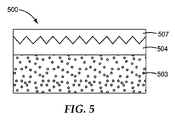


Classifications
-
- B—PERFORMING OPERATIONS; TRANSPORTING
- B44—DECORATIVE ARTS
- B44C—PRODUCING DECORATIVE EFFECTS; MOSAICS; TARSIA WORK; PAPERHANGING
- B44C1/00—Processes, not specifically provided for elsewhere, for producing decorative surface effects
- B44C1/16—Processes, not specifically provided for elsewhere, for producing decorative surface effects for applying transfer pictures or the like
- B44C1/165—Processes, not specifically provided for elsewhere, for producing decorative surface effects for applying transfer pictures or the like for decalcomanias; sheet material therefor
- B44C1/17—Dry transfer
-
- B—PERFORMING OPERATIONS; TRANSPORTING
- B32—LAYERED PRODUCTS
- B32B—LAYERED PRODUCTS, i.e. PRODUCTS BUILT-UP OF STRATA OF FLAT OR NON-FLAT, e.g. CELLULAR OR HONEYCOMB, FORM
- B32B15/00—Layered products comprising a layer of metal
- B32B15/04—Layered products comprising a layer of metal comprising metal as the main or only constituent of a layer, which is next to another layer of the same or of a different material
- B32B15/08—Layered products comprising a layer of metal comprising metal as the main or only constituent of a layer, which is next to another layer of the same or of a different material of synthetic resin
-
- B—PERFORMING OPERATIONS; TRANSPORTING
- B32—LAYERED PRODUCTS
- B32B—LAYERED PRODUCTS, i.e. PRODUCTS BUILT-UP OF STRATA OF FLAT OR NON-FLAT, e.g. CELLULAR OR HONEYCOMB, FORM
- B32B27/00—Layered products comprising a layer of synthetic resin
- B32B27/06—Layered products comprising a layer of synthetic resin as the main or only constituent of a layer, which is next to another layer of the same or of a different material
- B32B27/08—Layered products comprising a layer of synthetic resin as the main or only constituent of a layer, which is next to another layer of the same or of a different material of synthetic resin
-
- B—PERFORMING OPERATIONS; TRANSPORTING
- B32—LAYERED PRODUCTS
- B32B—LAYERED PRODUCTS, i.e. PRODUCTS BUILT-UP OF STRATA OF FLAT OR NON-FLAT, e.g. CELLULAR OR HONEYCOMB, FORM
- B32B27/00—Layered products comprising a layer of synthetic resin
- B32B27/06—Layered products comprising a layer of synthetic resin as the main or only constituent of a layer, which is next to another layer of the same or of a different material
- B32B27/10—Layered products comprising a layer of synthetic resin as the main or only constituent of a layer, which is next to another layer of the same or of a different material of paper or cardboard
-
- B—PERFORMING OPERATIONS; TRANSPORTING
- B32—LAYERED PRODUCTS
- B32B—LAYERED PRODUCTS, i.e. PRODUCTS BUILT-UP OF STRATA OF FLAT OR NON-FLAT, e.g. CELLULAR OR HONEYCOMB, FORM
- B32B27/00—Layered products comprising a layer of synthetic resin
- B32B27/12—Layered products comprising a layer of synthetic resin next to a fibrous or filamentary layer
-
- B—PERFORMING OPERATIONS; TRANSPORTING
- B32—LAYERED PRODUCTS
- B32B—LAYERED PRODUCTS, i.e. PRODUCTS BUILT-UP OF STRATA OF FLAT OR NON-FLAT, e.g. CELLULAR OR HONEYCOMB, FORM
- B32B27/00—Layered products comprising a layer of synthetic resin
- B32B27/28—Layered products comprising a layer of synthetic resin comprising synthetic resins not wholly covered by any one of the sub-groups B32B27/30 - B32B27/42
- B32B27/281—Layered products comprising a layer of synthetic resin comprising synthetic resins not wholly covered by any one of the sub-groups B32B27/30 - B32B27/42 comprising polyimides
-
- B—PERFORMING OPERATIONS; TRANSPORTING
- B32—LAYERED PRODUCTS
- B32B—LAYERED PRODUCTS, i.e. PRODUCTS BUILT-UP OF STRATA OF FLAT OR NON-FLAT, e.g. CELLULAR OR HONEYCOMB, FORM
- B32B27/00—Layered products comprising a layer of synthetic resin
- B32B27/30—Layered products comprising a layer of synthetic resin comprising vinyl (co)polymers; comprising acrylic (co)polymers
- B32B27/304—Layered products comprising a layer of synthetic resin comprising vinyl (co)polymers; comprising acrylic (co)polymers comprising vinyl halide (co)polymers, e.g. PVC, PVDC, PVF, PVDF
-
- B—PERFORMING OPERATIONS; TRANSPORTING
- B32—LAYERED PRODUCTS
- B32B—LAYERED PRODUCTS, i.e. PRODUCTS BUILT-UP OF STRATA OF FLAT OR NON-FLAT, e.g. CELLULAR OR HONEYCOMB, FORM
- B32B27/00—Layered products comprising a layer of synthetic resin
- B32B27/30—Layered products comprising a layer of synthetic resin comprising vinyl (co)polymers; comprising acrylic (co)polymers
- B32B27/306—Layered products comprising a layer of synthetic resin comprising vinyl (co)polymers; comprising acrylic (co)polymers comprising vinyl acetate or vinyl alcohol (co)polymers
-
- B—PERFORMING OPERATIONS; TRANSPORTING
- B32—LAYERED PRODUCTS
- B32B—LAYERED PRODUCTS, i.e. PRODUCTS BUILT-UP OF STRATA OF FLAT OR NON-FLAT, e.g. CELLULAR OR HONEYCOMB, FORM
- B32B27/00—Layered products comprising a layer of synthetic resin
- B32B27/30—Layered products comprising a layer of synthetic resin comprising vinyl (co)polymers; comprising acrylic (co)polymers
- B32B27/308—Layered products comprising a layer of synthetic resin comprising vinyl (co)polymers; comprising acrylic (co)polymers comprising acrylic (co)polymers
-
- B—PERFORMING OPERATIONS; TRANSPORTING
- B32—LAYERED PRODUCTS
- B32B—LAYERED PRODUCTS, i.e. PRODUCTS BUILT-UP OF STRATA OF FLAT OR NON-FLAT, e.g. CELLULAR OR HONEYCOMB, FORM
- B32B27/00—Layered products comprising a layer of synthetic resin
- B32B27/32—Layered products comprising a layer of synthetic resin comprising polyolefins
- B32B27/322—Layered products comprising a layer of synthetic resin comprising polyolefins comprising halogenated polyolefins, e.g. PTFE
-
- B—PERFORMING OPERATIONS; TRANSPORTING
- B32—LAYERED PRODUCTS
- B32B—LAYERED PRODUCTS, i.e. PRODUCTS BUILT-UP OF STRATA OF FLAT OR NON-FLAT, e.g. CELLULAR OR HONEYCOMB, FORM
- B32B27/00—Layered products comprising a layer of synthetic resin
- B32B27/34—Layered products comprising a layer of synthetic resin comprising polyamides
-
- B—PERFORMING OPERATIONS; TRANSPORTING
- B32—LAYERED PRODUCTS
- B32B—LAYERED PRODUCTS, i.e. PRODUCTS BUILT-UP OF STRATA OF FLAT OR NON-FLAT, e.g. CELLULAR OR HONEYCOMB, FORM
- B32B27/00—Layered products comprising a layer of synthetic resin
- B32B27/36—Layered products comprising a layer of synthetic resin comprising polyesters
- B32B27/365—Layered products comprising a layer of synthetic resin comprising polyesters comprising polycarbonates
-
- B—PERFORMING OPERATIONS; TRANSPORTING
- B32—LAYERED PRODUCTS
- B32B—LAYERED PRODUCTS, i.e. PRODUCTS BUILT-UP OF STRATA OF FLAT OR NON-FLAT, e.g. CELLULAR OR HONEYCOMB, FORM
- B32B27/00—Layered products comprising a layer of synthetic resin
- B32B27/42—Layered products comprising a layer of synthetic resin comprising condensation resins of aldehydes, e.g. with phenols, ureas or melamines
-
- B—PERFORMING OPERATIONS; TRANSPORTING
- B32—LAYERED PRODUCTS
- B32B—LAYERED PRODUCTS, i.e. PRODUCTS BUILT-UP OF STRATA OF FLAT OR NON-FLAT, e.g. CELLULAR OR HONEYCOMB, FORM
- B32B29/00—Layered products comprising a layer of paper or cardboard
- B32B29/002—Layered products comprising a layer of paper or cardboard as the main or only constituent of a layer, which is next to another layer of the same or of a different material
-
- B—PERFORMING OPERATIONS; TRANSPORTING
- B32—LAYERED PRODUCTS
- B32B—LAYERED PRODUCTS, i.e. PRODUCTS BUILT-UP OF STRATA OF FLAT OR NON-FLAT, e.g. CELLULAR OR HONEYCOMB, FORM
- B32B37/00—Methods or apparatus for laminating, e.g. by curing or by ultrasonic bonding
- B32B37/02—Methods or apparatus for laminating, e.g. by curing or by ultrasonic bonding characterised by a sequence of laminating steps, e.g. by adding new layers at consecutive laminating stations
- B32B37/025—Transfer laminating
-
- B—PERFORMING OPERATIONS; TRANSPORTING
- B32—LAYERED PRODUCTS
- B32B—LAYERED PRODUCTS, i.e. PRODUCTS BUILT-UP OF STRATA OF FLAT OR NON-FLAT, e.g. CELLULAR OR HONEYCOMB, FORM
- B32B5/00—Layered products characterised by the non- homogeneity or physical structure, i.e. comprising a fibrous, filamentary, particulate or foam layer; Layered products characterised by having a layer differing constitutionally or physically in different parts
- B32B5/02—Layered products characterised by the non- homogeneity or physical structure, i.e. comprising a fibrous, filamentary, particulate or foam layer; Layered products characterised by having a layer differing constitutionally or physically in different parts characterised by structural features of a fibrous or filamentary layer
- B32B5/022—Non-woven fabric
-
- B—PERFORMING OPERATIONS; TRANSPORTING
- B32—LAYERED PRODUCTS
- B32B—LAYERED PRODUCTS, i.e. PRODUCTS BUILT-UP OF STRATA OF FLAT OR NON-FLAT, e.g. CELLULAR OR HONEYCOMB, FORM
- B32B5/00—Layered products characterised by the non- homogeneity or physical structure, i.e. comprising a fibrous, filamentary, particulate or foam layer; Layered products characterised by having a layer differing constitutionally or physically in different parts
- B32B5/02—Layered products characterised by the non- homogeneity or physical structure, i.e. comprising a fibrous, filamentary, particulate or foam layer; Layered products characterised by having a layer differing constitutionally or physically in different parts characterised by structural features of a fibrous or filamentary layer
- B32B5/024—Woven fabric
-
- B—PERFORMING OPERATIONS; TRANSPORTING
- B32—LAYERED PRODUCTS
- B32B—LAYERED PRODUCTS, i.e. PRODUCTS BUILT-UP OF STRATA OF FLAT OR NON-FLAT, e.g. CELLULAR OR HONEYCOMB, FORM
- B32B7/00—Layered products characterised by the relation between layers; Layered products characterised by the relative orientation of features between layers, or by the relative values of a measurable parameter between layers, i.e. products comprising layers having different physical, chemical or physicochemical properties; Layered products characterised by the interconnection of layers
- B32B7/04—Interconnection of layers
- B32B7/06—Interconnection of layers permitting easy separation
-
- B—PERFORMING OPERATIONS; TRANSPORTING
- B32—LAYERED PRODUCTS
- B32B—LAYERED PRODUCTS, i.e. PRODUCTS BUILT-UP OF STRATA OF FLAT OR NON-FLAT, e.g. CELLULAR OR HONEYCOMB, FORM
- B32B7/00—Layered products characterised by the relation between layers; Layered products characterised by the relative orientation of features between layers, or by the relative values of a measurable parameter between layers, i.e. products comprising layers having different physical, chemical or physicochemical properties; Layered products characterised by the interconnection of layers
- B32B7/04—Interconnection of layers
- B32B7/12—Interconnection of layers using interposed adhesives or interposed materials with bonding properties
-
- H—ELECTRICITY
- H10—SEMICONDUCTOR DEVICES; ELECTRIC SOLID-STATE DEVICES NOT OTHERWISE PROVIDED FOR
- H10K—ORGANIC ELECTRIC SOLID-STATE DEVICES
- H10K50/00—Organic light-emitting devices
- H10K50/80—Constructional details
- H10K50/85—Arrangements for extracting light from the devices
- H10K50/858—Arrangements for extracting light from the devices comprising refractive means, e.g. lenses
-
- H—ELECTRICITY
- H10—SEMICONDUCTOR DEVICES; ELECTRIC SOLID-STATE DEVICES NOT OTHERWISE PROVIDED FOR
- H10K—ORGANIC ELECTRIC SOLID-STATE DEVICES
- H10K59/00—Integrated devices, or assemblies of multiple devices, comprising at least one organic light-emitting element covered by group H10K50/00
- H10K59/80—Constructional details
- H10K59/875—Arrangements for extracting light from the devices
- H10K59/879—Arrangements for extracting light from the devices comprising refractive means, e.g. lenses
-
- B—PERFORMING OPERATIONS; TRANSPORTING
- B32—LAYERED PRODUCTS
- B32B—LAYERED PRODUCTS, i.e. PRODUCTS BUILT-UP OF STRATA OF FLAT OR NON-FLAT, e.g. CELLULAR OR HONEYCOMB, FORM
- B32B2255/00—Coating on the layer surface
- B32B2255/12—Coating on the layer surface on paper layer
-
- B—PERFORMING OPERATIONS; TRANSPORTING
- B32—LAYERED PRODUCTS
- B32B—LAYERED PRODUCTS, i.e. PRODUCTS BUILT-UP OF STRATA OF FLAT OR NON-FLAT, e.g. CELLULAR OR HONEYCOMB, FORM
- B32B2255/00—Coating on the layer surface
- B32B2255/26—Polymeric coating
-
- B—PERFORMING OPERATIONS; TRANSPORTING
- B32—LAYERED PRODUCTS
- B32B—LAYERED PRODUCTS, i.e. PRODUCTS BUILT-UP OF STRATA OF FLAT OR NON-FLAT, e.g. CELLULAR OR HONEYCOMB, FORM
- B32B2264/00—Composition or properties of particles which form a particulate layer or are present as additives
- B32B2264/10—Inorganic particles
- B32B2264/107—Ceramic
- B32B2264/108—Carbon, e.g. graphite particles
-
- B—PERFORMING OPERATIONS; TRANSPORTING
- B32—LAYERED PRODUCTS
- B32B—LAYERED PRODUCTS, i.e. PRODUCTS BUILT-UP OF STRATA OF FLAT OR NON-FLAT, e.g. CELLULAR OR HONEYCOMB, FORM
- B32B2274/00—Thermoplastic elastomer material
-
- B—PERFORMING OPERATIONS; TRANSPORTING
- B32—LAYERED PRODUCTS
- B32B—LAYERED PRODUCTS, i.e. PRODUCTS BUILT-UP OF STRATA OF FLAT OR NON-FLAT, e.g. CELLULAR OR HONEYCOMB, FORM
- B32B2307/00—Properties of the layers or laminate
- B32B2307/30—Properties of the layers or laminate having particular thermal properties
- B32B2307/308—Heat stability
-
- B—PERFORMING OPERATIONS; TRANSPORTING
- B32—LAYERED PRODUCTS
- B32B—LAYERED PRODUCTS, i.e. PRODUCTS BUILT-UP OF STRATA OF FLAT OR NON-FLAT, e.g. CELLULAR OR HONEYCOMB, FORM
- B32B2307/00—Properties of the layers or laminate
- B32B2307/40—Properties of the layers or laminate having particular optical properties
- B32B2307/412—Transparent
-
- B—PERFORMING OPERATIONS; TRANSPORTING
- B32—LAYERED PRODUCTS
- B32B—LAYERED PRODUCTS, i.e. PRODUCTS BUILT-UP OF STRATA OF FLAT OR NON-FLAT, e.g. CELLULAR OR HONEYCOMB, FORM
- B32B2307/00—Properties of the layers or laminate
- B32B2307/40—Properties of the layers or laminate having particular optical properties
- B32B2307/418—Refractive
-
- B—PERFORMING OPERATIONS; TRANSPORTING
- B32—LAYERED PRODUCTS
- B32B—LAYERED PRODUCTS, i.e. PRODUCTS BUILT-UP OF STRATA OF FLAT OR NON-FLAT, e.g. CELLULAR OR HONEYCOMB, FORM
- B32B2307/00—Properties of the layers or laminate
- B32B2307/50—Properties of the layers or laminate having particular mechanical properties
- B32B2307/538—Roughness
-
- B—PERFORMING OPERATIONS; TRANSPORTING
- B32—LAYERED PRODUCTS
- B32B—LAYERED PRODUCTS, i.e. PRODUCTS BUILT-UP OF STRATA OF FLAT OR NON-FLAT, e.g. CELLULAR OR HONEYCOMB, FORM
- B32B2307/00—Properties of the layers or laminate
- B32B2307/70—Other properties
- B32B2307/704—Crystalline
-
- B—PERFORMING OPERATIONS; TRANSPORTING
- B32—LAYERED PRODUCTS
- B32B—LAYERED PRODUCTS, i.e. PRODUCTS BUILT-UP OF STRATA OF FLAT OR NON-FLAT, e.g. CELLULAR OR HONEYCOMB, FORM
- B32B2307/00—Properties of the layers or laminate
- B32B2307/70—Other properties
- B32B2307/714—Inert, i.e. inert to chemical degradation, corrosion
-
- B—PERFORMING OPERATIONS; TRANSPORTING
- B32—LAYERED PRODUCTS
- B32B—LAYERED PRODUCTS, i.e. PRODUCTS BUILT-UP OF STRATA OF FLAT OR NON-FLAT, e.g. CELLULAR OR HONEYCOMB, FORM
- B32B2307/00—Properties of the layers or laminate
- B32B2307/70—Other properties
- B32B2307/732—Dimensional properties
-
- B—PERFORMING OPERATIONS; TRANSPORTING
- B32—LAYERED PRODUCTS
- B32B—LAYERED PRODUCTS, i.e. PRODUCTS BUILT-UP OF STRATA OF FLAT OR NON-FLAT, e.g. CELLULAR OR HONEYCOMB, FORM
- B32B2307/00—Properties of the layers or laminate
- B32B2307/70—Other properties
- B32B2307/732—Dimensional properties
- B32B2307/734—Dimensional stability
-
- B—PERFORMING OPERATIONS; TRANSPORTING
- B32—LAYERED PRODUCTS
- B32B—LAYERED PRODUCTS, i.e. PRODUCTS BUILT-UP OF STRATA OF FLAT OR NON-FLAT, e.g. CELLULAR OR HONEYCOMB, FORM
- B32B2309/00—Parameters for the laminating or treatment process; Apparatus details
- B32B2309/02—Temperature
-
- B—PERFORMING OPERATIONS; TRANSPORTING
- B32—LAYERED PRODUCTS
- B32B—LAYERED PRODUCTS, i.e. PRODUCTS BUILT-UP OF STRATA OF FLAT OR NON-FLAT, e.g. CELLULAR OR HONEYCOMB, FORM
- B32B2309/00—Parameters for the laminating or treatment process; Apparatus details
- B32B2309/04—Time
-
- B—PERFORMING OPERATIONS; TRANSPORTING
- B32—LAYERED PRODUCTS
- B32B—LAYERED PRODUCTS, i.e. PRODUCTS BUILT-UP OF STRATA OF FLAT OR NON-FLAT, e.g. CELLULAR OR HONEYCOMB, FORM
- B32B2457/00—Electrical equipment
- B32B2457/12—Photovoltaic modules
-
- B—PERFORMING OPERATIONS; TRANSPORTING
- B32—LAYERED PRODUCTS
- B32B—LAYERED PRODUCTS, i.e. PRODUCTS BUILT-UP OF STRATA OF FLAT OR NON-FLAT, e.g. CELLULAR OR HONEYCOMB, FORM
- B32B2457/00—Electrical equipment
- B32B2457/20—Displays, e.g. liquid crystal displays, plasma displays
-
- B—PERFORMING OPERATIONS; TRANSPORTING
- B32—LAYERED PRODUCTS
- B32B—LAYERED PRODUCTS, i.e. PRODUCTS BUILT-UP OF STRATA OF FLAT OR NON-FLAT, e.g. CELLULAR OR HONEYCOMB, FORM
- B32B37/00—Methods or apparatus for laminating, e.g. by curing or by ultrasonic bonding
- B32B37/10—Methods or apparatus for laminating, e.g. by curing or by ultrasonic bonding characterised by the pressing technique, e.g. using action of vacuum or fluid pressure
- B32B37/1009—Methods or apparatus for laminating, e.g. by curing or by ultrasonic bonding characterised by the pressing technique, e.g. using action of vacuum or fluid pressure using vacuum and fluid pressure
-
- H—ELECTRICITY
- H10—SEMICONDUCTOR DEVICES; ELECTRIC SOLID-STATE DEVICES NOT OTHERWISE PROVIDED FOR
- H10K—ORGANIC ELECTRIC SOLID-STATE DEVICES
- H10K71/00—Manufacture or treatment specially adapted for the organic devices covered by this subclass
- H10K71/80—Manufacture or treatment specially adapted for the organic devices covered by this subclass using temporary substrates
-
- Y—GENERAL TAGGING OF NEW TECHNOLOGICAL DEVELOPMENTS; GENERAL TAGGING OF CROSS-SECTIONAL TECHNOLOGIES SPANNING OVER SEVERAL SECTIONS OF THE IPC; TECHNICAL SUBJECTS COVERED BY FORMER USPC CROSS-REFERENCE ART COLLECTIONS [XRACs] AND DIGESTS
- Y10—TECHNICAL SUBJECTS COVERED BY FORMER USPC
- Y10T—TECHNICAL SUBJECTS COVERED BY FORMER US CLASSIFICATION
- Y10T156/00—Adhesive bonding and miscellaneous chemical manufacture
- Y10T156/10—Methods of surface bonding and/or assembly therefor
-
- Y—GENERAL TAGGING OF NEW TECHNOLOGICAL DEVELOPMENTS; GENERAL TAGGING OF CROSS-SECTIONAL TECHNOLOGIES SPANNING OVER SEVERAL SECTIONS OF THE IPC; TECHNICAL SUBJECTS COVERED BY FORMER USPC CROSS-REFERENCE ART COLLECTIONS [XRACs] AND DIGESTS
- Y10—TECHNICAL SUBJECTS COVERED BY FORMER USPC
- Y10T—TECHNICAL SUBJECTS COVERED BY FORMER US CLASSIFICATION
- Y10T428/00—Stock material or miscellaneous articles
- Y10T428/24—Structurally defined web or sheet [e.g., overall dimension, etc.]
- Y10T428/24479—Structurally defined web or sheet [e.g., overall dimension, etc.] including variation in thickness
- Y10T428/24521—Structurally defined web or sheet [e.g., overall dimension, etc.] including variation in thickness with component conforming to contour of nonplanar surface
- Y10T428/24545—Containing metal or metal compound
Landscapes
- Engineering & Computer Science (AREA)
- Textile Engineering (AREA)
- Physics & Mathematics (AREA)
- Optics & Photonics (AREA)
- Laminated Bodies (AREA)
- Chemical & Material Sciences (AREA)
- Crystallography & Structural Chemistry (AREA)
- Nanotechnology (AREA)
Applications Claiming Priority (3)
| Application Number | Priority Date | Filing Date | Title |
|---|---|---|---|
| US13/778,276 | 2013-02-27 | ||
| US13/778,276 US20140242343A1 (en) | 2013-02-27 | 2013-02-27 | Lamination transfer films for forming embedded nanostructures |
| PCT/US2014/016668 WO2014133799A1 (en) | 2013-02-27 | 2014-02-17 | Lamination transfer films for forming embedded nanostructures |
Publications (2)
| Publication Number | Publication Date |
|---|---|
| JP2016515954A true JP2016515954A (ja) | 2016-06-02 |
| JP2016515954A5 JP2016515954A5 (enExample) | 2017-03-16 |
Family
ID=51388438
Family Applications (1)
| Application Number | Title | Priority Date | Filing Date |
|---|---|---|---|
| JP2015560207A Pending JP2016515954A (ja) | 2013-02-27 | 2014-02-17 | 埋め込まれたナノ構造を形成するための積層転写フィルム |
Country Status (7)
| Country | Link |
|---|---|
| US (1) | US20140242343A1 (enExample) |
| EP (2) | EP3332964B1 (enExample) |
| JP (1) | JP2016515954A (enExample) |
| KR (1) | KR20150123251A (enExample) |
| CN (1) | CN105899359B (enExample) |
| TW (1) | TW201446524A (enExample) |
| WO (1) | WO2014133799A1 (enExample) |
Cited By (2)
| Publication number | Priority date | Publication date | Assignee | Title |
|---|---|---|---|---|
| JPWO2020066338A1 (ja) * | 2018-09-28 | 2021-05-20 | 富士フイルム株式会社 | 転写材料、積層体、及び、積層体の製造方法 |
| JPWO2020066376A1 (ja) * | 2018-09-28 | 2021-08-30 | 富士フイルム株式会社 | Ledディスプレイのフロント部材、及び、その製造方法 |
Families Citing this family (41)
| Publication number | Priority date | Publication date | Assignee | Title |
|---|---|---|---|---|
| EP2624326A4 (en) * | 2010-09-29 | 2017-05-10 | Posco | Method for manufacturing a flexible electronic device using a roll-shaped motherboard, flexible electronic device, and flexible substrate |
| US9878954B2 (en) | 2013-09-13 | 2018-01-30 | 3M Innovative Properties Company | Vacuum glazing pillars for insulated glass units |
| CN104516576B (zh) | 2013-09-29 | 2016-04-13 | 宸鸿科技(厦门)有限公司 | 触控面板的制作方法 |
| US9246134B2 (en) * | 2014-01-20 | 2016-01-26 | 3M Innovative Properties Company | Lamination transfer films for forming articles with engineered voids |
| US20150202834A1 (en) | 2014-01-20 | 2015-07-23 | 3M Innovative Properties Company | Lamination transfer films for forming antireflective structures |
| US10220600B2 (en) | 2014-01-20 | 2019-03-05 | 3M Innovative Properties Company | Lamination transfer films for forming reentrant structures |
| WO2015112711A1 (en) | 2014-01-22 | 2015-07-30 | 3M Innovative Properties Company | Microoptics for glazing |
| TW201539736A (zh) | 2014-03-19 | 2015-10-16 | 3M新設資產公司 | 用於藉白光成色之 oled 裝置的奈米結構 |
| TWI664077B (zh) * | 2014-04-09 | 2019-07-01 | 美商陶氏有機矽公司 | 疏水物件 |
| US9202953B1 (en) * | 2014-05-16 | 2015-12-01 | National Cheng Kung University | Method for manufacturing solar cell with nano-structural film |
| US9995944B2 (en) | 2014-06-13 | 2018-06-12 | 3M Innovative Properties Company | Optical stacks for sparkle reduction |
| US9472788B2 (en) | 2014-08-27 | 2016-10-18 | 3M Innovative Properties Company | Thermally-assisted self-assembly method of nanoparticles and nanowires within engineered periodic structures |
| US9586385B2 (en) * | 2014-08-27 | 2017-03-07 | 3M Innovative Properties Company | Inorganic multilayer lamination transfer films |
| CN106660355B (zh) | 2014-08-27 | 2019-10-11 | 3M创新有限公司 | 电多层层合转印膜 |
| EP3209841B1 (en) * | 2014-10-20 | 2021-04-07 | 3M Innovative Properties Company | Insulated glazing units and microoptical layer comprising microstructured diffuser and methods |
| US9942979B2 (en) * | 2014-11-03 | 2018-04-10 | Samsung Electronics Co., Ltd. | Flexible printed circuit board |
| US10518512B2 (en) | 2015-03-31 | 2019-12-31 | 3M Innovative Properties Company | Method of forming dual-cure nanostructure transfer film |
| US10106643B2 (en) * | 2015-03-31 | 2018-10-23 | 3M Innovative Properties Company | Dual-cure nanostructure transfer film |
| WO2016205189A1 (en) | 2015-06-19 | 2016-12-22 | 3M Innovative Properties Company | Micro-optical assemblies including transparent substrates having graphic layer and method of making thereof |
| EP3311430B1 (en) | 2015-06-19 | 2019-12-18 | 3M Innovative Properties Company | Segmented transfer tape and method of making the same |
| CN107820461B (zh) | 2015-06-19 | 2019-12-17 | 3M创新有限公司 | 分段式转印带及其制备和使用方法 |
| KR102433790B1 (ko) * | 2015-07-07 | 2022-08-18 | 삼성디스플레이 주식회사 | 전극, 그 제조 방법 및 이를 포함하는 유기 발광 표시 장치 |
| TWI538581B (zh) | 2015-11-20 | 2016-06-11 | 財團法人工業技術研究院 | 金屬導體結構及線路結構 |
| JP6960407B2 (ja) | 2015-12-28 | 2021-11-05 | スリーエム イノベイティブ プロパティズ カンパニー | 微細構造化層を有する物品 |
| US11312100B2 (en) | 2015-12-28 | 2022-04-26 | 3M Innovative Properties Company | Article with microstructured layer |
| EP3244442B1 (en) * | 2016-05-09 | 2022-08-03 | Emberion Oy | A method of forming a device comprising quantum dots |
| CN109476964B (zh) * | 2016-07-22 | 2022-04-26 | 3M创新有限公司 | 作为陶瓷前体的聚合物粘合剂层 |
| JP7056878B2 (ja) * | 2016-09-21 | 2022-04-19 | スリーエム イノベイティブ プロパティズ カンパニー | ガラスを含む保護ディスプレイフィルム |
| DE102017108573A1 (de) * | 2017-04-21 | 2018-10-25 | Osram Opto Semiconductors Gmbh | Optoelektronisches Bauelement und Verfahren zur Herstellung eines optoelektronischen Bauelements |
| WO2019026209A1 (ja) * | 2017-08-02 | 2019-02-07 | シャープ株式会社 | 可撓性表示装置及び可撓性表示装置の製造方法 |
| CN111032348A (zh) * | 2017-08-31 | 2020-04-17 | 3M创新有限公司 | 包含部分地嵌入的微球体的成型转移制品、由其制得的成型成品以及制备方法 |
| TWI645973B (zh) * | 2017-12-15 | 2019-01-01 | 律勝科技股份有限公司 | 聚醯亞胺薄化軟性基板及其製造方法 |
| CN109700440A (zh) * | 2018-12-18 | 2019-05-03 | 中北大学 | 柔性可穿戴传感器及其相应的可穿戴设备及制备方法 |
| KR102342295B1 (ko) * | 2018-12-31 | 2021-12-22 | 한양대학교 산학협력단 | 기판 탈착 방법 및 전자 소자의 제조 방법 |
| CN112126151A (zh) * | 2019-06-25 | 2020-12-25 | 苏州星烁纳米科技有限公司 | 量子点-聚合物复合体的制备方法及量子点膜的制备方法 |
| TWI794527B (zh) | 2019-07-10 | 2023-03-01 | 國立成功大學 | 包含由微結構控制物理性質之裝置及其製造方法 |
| US12161013B2 (en) | 2019-09-18 | 2024-12-03 | 3M Innovative Properties Company | Articles including nanostructured surfaces and enclosed voids, and methods of making same |
| CN111268722B (zh) * | 2020-02-28 | 2023-05-26 | 东南大学 | 一种原位常温制备垂直阵列结构二硫化锡的方法 |
| US11825568B2 (en) * | 2021-04-01 | 2023-11-21 | Whirlpool Corporation | Segmented thermoresistive heating system |
| CN116024606B (zh) * | 2022-12-26 | 2023-07-28 | 青岛科技大学 | 一种富缺陷的Ru-Cu无定形纳米材料的制备 |
| WO2025140916A1 (en) * | 2023-12-27 | 2025-07-03 | Merck Patent Gmbh | Method of manufacturing acoustic wave device |
Citations (4)
| Publication number | Priority date | Publication date | Assignee | Title |
|---|---|---|---|---|
| JP2001105525A (ja) * | 1999-10-14 | 2001-04-17 | East Japan Railway Co | 化粧性部材、その製造方法及び用途 |
| JP2002087893A (ja) * | 2000-09-13 | 2002-03-27 | Inax Corp | 微細凹凸又は粗化面を有する基体表面に親水性防汚層を有するタイル及びその製造方法 |
| JP2004123831A (ja) * | 2002-09-30 | 2004-04-22 | Dainippon Printing Co Ltd | 光硬化性樹脂組成物、微細凹凸パターン転写箔、光学物品、スタンパー及び微細凹凸パターンの形成方法 |
| JP2010052408A (ja) * | 2008-08-30 | 2010-03-11 | Nagaoka Univ Of Technology | 表面に微細凹凸パターンを有したセラミックス焼成体及びその製造方法 |
Family Cites Families (32)
| Publication number | Priority date | Publication date | Assignee | Title |
|---|---|---|---|---|
| US4567073A (en) | 1982-07-02 | 1986-01-28 | Minnesota Mining And Manufacturing Company | Composite low surface energy liner of perfluoropolyether |
| US4472480A (en) | 1982-07-02 | 1984-09-18 | Minnesota Mining And Manufacturing Company | Low surface energy liner of perfluoropolyether |
| US4614667A (en) | 1984-05-21 | 1986-09-30 | Minnesota Mining And Manufacturing Company | Composite low surface energy liner of perfluoropolyether |
| US4766023A (en) | 1987-01-16 | 1988-08-23 | Minnesota Mining And Manufacturing Company | Method for making a flexible louvered plastic film with protective coatings and film produced thereby |
| JP3444053B2 (ja) | 1995-10-13 | 2003-09-08 | ソニー株式会社 | 薄膜半導体装置 |
| US6376590B2 (en) | 1999-10-28 | 2002-04-23 | 3M Innovative Properties Company | Zirconia sol, process of making and composite material |
| US6521324B1 (en) * | 1999-11-30 | 2003-02-18 | 3M Innovative Properties Company | Thermal transfer of microstructured layers |
| US6398370B1 (en) | 2000-11-15 | 2002-06-04 | 3M Innovative Properties Company | Light control device |
| US6858253B2 (en) | 2001-05-31 | 2005-02-22 | 3M Innovative Properties Company | Method of making dimensionally stable composite article |
| JP4436030B2 (ja) | 2002-05-10 | 2010-03-24 | スリーエム イノベイティブ プロパティズ カンパニー | アクリル系剥離剤前駆体、剥離剤物品及び剥離剤物品の製造方法 |
| US7241437B2 (en) | 2004-12-30 | 2007-07-10 | 3M Innovative Properties Company | Zirconia particles |
| DE102005017170B4 (de) * | 2005-04-13 | 2010-07-01 | Ovd Kinegram Ag | Transferfolie, Verfahren zu deren Herstellung sowie Mehrschichtkörper und dessen Verwendung |
| US20080024866A1 (en) * | 2006-07-28 | 2008-01-31 | Harald Walter | Zero-order diffractive filter |
| JP2008137187A (ja) * | 2006-11-30 | 2008-06-19 | Sumitomo Osaka Cement Co Ltd | 転写フィルム及び発光装置並びに転写フィルムの機能層形成用塗料 |
| JP4978188B2 (ja) * | 2006-12-28 | 2012-07-18 | 旭硝子株式会社 | 微細構造体の製造方法 |
| US8213082B2 (en) | 2007-12-21 | 2012-07-03 | 3M Innovative Properties Company | Light control film |
| TWI365812B (en) * | 2008-10-23 | 2012-06-11 | Compal Electronics Inc | Transfer film, method of manufacturing the same, transfer method and object surface structure |
| SG171872A1 (en) | 2008-12-15 | 2011-07-28 | 3M Innovative Properties Co | High refractive index inorganic oxide nanoparticles comprising surface treatment, polymerizable resin, and articles |
| US8222352B2 (en) * | 2008-12-24 | 2012-07-17 | Nitto Denko Corporation | Silicone resin composition |
| JP5573069B2 (ja) * | 2009-09-25 | 2014-08-20 | 大日本印刷株式会社 | 保護層転写シート |
| US8268067B2 (en) * | 2009-10-06 | 2012-09-18 | 3M Innovative Properties Company | Perfluoropolyether coating composition for hard surfaces |
| US8917447B2 (en) * | 2010-01-13 | 2014-12-23 | 3M Innovative Properties Company | Microreplicated film for attachment to autostereoscopic display components |
| US20130011608A1 (en) * | 2010-01-13 | 2013-01-10 | Wolk Martin B | Optical films with microstructured low refractive index nanovoided layers and methods therefor |
| DE102010004741B4 (de) * | 2010-01-14 | 2023-02-23 | Schott Ag | Verfahren zur Herstellung eines Verbundmaterials sowie Küchengerät |
| US8538224B2 (en) * | 2010-04-22 | 2013-09-17 | 3M Innovative Properties Company | OLED light extraction films having internal nanostructures and external microstructures |
| SG185417A1 (en) * | 2010-05-07 | 2012-12-28 | 3M Innovative Properties Co | Antireflective films comprising microstructured surface |
| JP6247533B2 (ja) * | 2010-10-06 | 2017-12-13 | スリーエム イノベイティブ プロパティズ カンパニー | ナノシリカ系コーティング及びバリア層を有する反射防止物品 |
| CN103249562B (zh) * | 2010-12-09 | 2015-07-08 | 旭化成电子材料株式会社 | 微细结构积层体、微细结构积层体的制作方法以及微细结构体的制造方法 |
| JP6033233B2 (ja) | 2010-12-17 | 2016-11-30 | スリーエム イノベイティブ プロパティズ カンパニー | マルチサイズ粒子を有する転写物品及び方法 |
| WO2012115132A1 (ja) * | 2011-02-24 | 2012-08-30 | 東レ株式会社 | 転写フィルム |
| EP2657299A4 (en) * | 2011-06-21 | 2014-03-12 | Asahi Kasei E Materials Corp | INORGANIC COMPOSITION FOR TRANSMITTING A MICROROLE STRUCTURE |
| US9780335B2 (en) | 2012-07-20 | 2017-10-03 | 3M Innovative Properties Company | Structured lamination transfer films and methods |
-
2013
- 2013-02-27 US US13/778,276 patent/US20140242343A1/en not_active Abandoned
-
2014
- 2014-02-17 WO PCT/US2014/016668 patent/WO2014133799A1/en not_active Ceased
- 2014-02-17 JP JP2015560207A patent/JP2016515954A/ja active Pending
- 2014-02-17 EP EP18150180.0A patent/EP3332964B1/en active Active
- 2014-02-17 KR KR1020157024311A patent/KR20150123251A/ko not_active Ceased
- 2014-02-17 CN CN201480010442.2A patent/CN105899359B/zh active Active
- 2014-02-17 EP EP14756801.8A patent/EP2961601B1/en active Active
- 2014-02-26 TW TW103106594A patent/TW201446524A/zh unknown
Patent Citations (4)
| Publication number | Priority date | Publication date | Assignee | Title |
|---|---|---|---|---|
| JP2001105525A (ja) * | 1999-10-14 | 2001-04-17 | East Japan Railway Co | 化粧性部材、その製造方法及び用途 |
| JP2002087893A (ja) * | 2000-09-13 | 2002-03-27 | Inax Corp | 微細凹凸又は粗化面を有する基体表面に親水性防汚層を有するタイル及びその製造方法 |
| JP2004123831A (ja) * | 2002-09-30 | 2004-04-22 | Dainippon Printing Co Ltd | 光硬化性樹脂組成物、微細凹凸パターン転写箔、光学物品、スタンパー及び微細凹凸パターンの形成方法 |
| JP2010052408A (ja) * | 2008-08-30 | 2010-03-11 | Nagaoka Univ Of Technology | 表面に微細凹凸パターンを有したセラミックス焼成体及びその製造方法 |
Cited By (4)
| Publication number | Priority date | Publication date | Assignee | Title |
|---|---|---|---|---|
| JPWO2020066338A1 (ja) * | 2018-09-28 | 2021-05-20 | 富士フイルム株式会社 | 転写材料、積層体、及び、積層体の製造方法 |
| JPWO2020066376A1 (ja) * | 2018-09-28 | 2021-08-30 | 富士フイルム株式会社 | Ledディスプレイのフロント部材、及び、その製造方法 |
| JP7057431B2 (ja) | 2018-09-28 | 2022-04-19 | 富士フイルム株式会社 | Ledディスプレイのフロント部材、及び、その製造方法 |
| JP7091463B2 (ja) | 2018-09-28 | 2022-06-27 | 富士フイルム株式会社 | 転写材料、積層体、及び、積層体の製造方法 |
Also Published As
| Publication number | Publication date |
|---|---|
| WO2014133799A1 (en) | 2014-09-04 |
| EP3332964A1 (en) | 2018-06-13 |
| EP2961601B1 (en) | 2021-12-08 |
| US20140242343A1 (en) | 2014-08-28 |
| EP2961601A4 (en) | 2017-07-05 |
| EP2961601A1 (en) | 2016-01-06 |
| EP3332964B1 (en) | 2022-10-05 |
| TW201446524A (zh) | 2014-12-16 |
| CN105899359A (zh) | 2016-08-24 |
| CN105899359B (zh) | 2018-03-09 |
| KR20150123251A (ko) | 2015-11-03 |
Similar Documents
| Publication | Publication Date | Title |
|---|---|---|
| EP2961601B1 (en) | Lamination transfer films for forming embedded nanostructures | |
| US10436946B2 (en) | Lamination transfer films for forming antireflective structures | |
| US10988979B2 (en) | Microoptics for glazing | |
| US9731473B2 (en) | Articles with lamination transfer films having engineered voids | |
| US10220600B2 (en) | Lamination transfer films for forming reentrant structures | |
| JP2017529302A (ja) | 設計された周期構造内のナノ粒子及びナノワイヤの熱支援自己集合方法 |
Legal Events
| Date | Code | Title | Description |
|---|---|---|---|
| A521 | Request for written amendment filed |
Free format text: JAPANESE INTERMEDIATE CODE: A523 Effective date: 20170207 |
|
| A621 | Written request for application examination |
Free format text: JAPANESE INTERMEDIATE CODE: A621 Effective date: 20170207 |
|
| A977 | Report on retrieval |
Free format text: JAPANESE INTERMEDIATE CODE: A971007 Effective date: 20171214 |
|
| A131 | Notification of reasons for refusal |
Free format text: JAPANESE INTERMEDIATE CODE: A131 Effective date: 20171219 |
|
| RD03 | Notification of appointment of power of attorney |
Free format text: JAPANESE INTERMEDIATE CODE: A7423 Effective date: 20171228 |
|
| RD04 | Notification of resignation of power of attorney |
Free format text: JAPANESE INTERMEDIATE CODE: A7424 Effective date: 20180110 |
|
| A601 | Written request for extension of time |
Free format text: JAPANESE INTERMEDIATE CODE: A601 Effective date: 20180315 |
|
| A02 | Decision of refusal |
Free format text: JAPANESE INTERMEDIATE CODE: A02 Effective date: 20180807 |