JP2016507902A - Multi-level metal coating on the ceramic substrate - Google Patents
Multi-level metal coating on the ceramic substrate Download PDFInfo
- Publication number
- JP2016507902A JP2016507902A JP2015556472A JP2015556472A JP2016507902A JP 2016507902 A JP2016507902 A JP 2016507902A JP 2015556472 A JP2015556472 A JP 2015556472A JP 2015556472 A JP2015556472 A JP 2015556472A JP 2016507902 A JP2016507902 A JP 2016507902A
- Authority
- JP
- Japan
- Prior art keywords
- power region
- ceramic substrate
- high power
- metal coating
- copper
- Prior art date
- Legal status (The legal status is an assumption and is not a legal conclusion. Google has not performed a legal analysis and makes no representation as to the accuracy of the status listed.)
- Pending
Links
Images
Classifications
-
- H—ELECTRICITY
- H05—ELECTRIC TECHNIQUES NOT OTHERWISE PROVIDED FOR
- H05K—PRINTED CIRCUITS; CASINGS OR CONSTRUCTIONAL DETAILS OF ELECTRIC APPARATUS; MANUFACTURE OF ASSEMBLAGES OF ELECTRICAL COMPONENTS
- H05K3/00—Apparatus or processes for manufacturing printed circuits
- H05K3/10—Apparatus or processes for manufacturing printed circuits in which conductive material is applied to the insulating support in such a manner as to form the desired conductive pattern
- H05K3/12—Apparatus or processes for manufacturing printed circuits in which conductive material is applied to the insulating support in such a manner as to form the desired conductive pattern using thick film techniques, e.g. printing techniques to apply the conductive material or similar techniques for applying conductive paste or ink patterns
- H05K3/1216—Apparatus or processes for manufacturing printed circuits in which conductive material is applied to the insulating support in such a manner as to form the desired conductive pattern using thick film techniques, e.g. printing techniques to apply the conductive material or similar techniques for applying conductive paste or ink patterns by screen printing or stencil printing
-
- C—CHEMISTRY; METALLURGY
- C22—METALLURGY; FERROUS OR NON-FERROUS ALLOYS; TREATMENT OF ALLOYS OR NON-FERROUS METALS
- C22F—CHANGING THE PHYSICAL STRUCTURE OF NON-FERROUS METALS AND NON-FERROUS ALLOYS
- C22F1/00—Changing the physical structure of non-ferrous metals or alloys by heat treatment or by hot or cold working
- C22F1/08—Changing the physical structure of non-ferrous metals or alloys by heat treatment or by hot or cold working of copper or alloys based thereon
-
- H—ELECTRICITY
- H01—ELECTRIC ELEMENTS
- H01L—SEMICONDUCTOR DEVICES NOT COVERED BY CLASS H10
- H01L21/00—Processes or apparatus adapted for the manufacture or treatment of semiconductor or solid state devices or of parts thereof
- H01L21/02—Manufacture or treatment of semiconductor devices or of parts thereof
- H01L21/04—Manufacture or treatment of semiconductor devices or of parts thereof the devices having at least one potential-jump barrier or surface barrier, e.g. PN junction, depletion layer or carrier concentration layer
- H01L21/48—Manufacture or treatment of parts, e.g. containers, prior to assembly of the devices, using processes not provided for in a single one of the subgroups H01L21/06 - H01L21/326
- H01L21/4814—Conductive parts
- H01L21/4846—Leads on or in insulating or insulated substrates, e.g. metallisation
- H01L21/4867—Applying pastes or inks, e.g. screen printing
-
- H—ELECTRICITY
- H01—ELECTRIC ELEMENTS
- H01L—SEMICONDUCTOR DEVICES NOT COVERED BY CLASS H10
- H01L23/00—Details of semiconductor or other solid state devices
- H01L23/48—Arrangements for conducting electric current to or from the solid state body in operation, e.g. leads, terminal arrangements ; Selection of materials therefor
- H01L23/488—Arrangements for conducting electric current to or from the solid state body in operation, e.g. leads, terminal arrangements ; Selection of materials therefor consisting of soldered or bonded constructions
- H01L23/498—Leads, i.e. metallisations or lead-frames on insulating substrates, e.g. chip carriers
- H01L23/49838—Geometry or layout
- H01L23/49844—Geometry or layout for devices being provided for in H01L29/00
-
- H—ELECTRICITY
- H05—ELECTRIC TECHNIQUES NOT OTHERWISE PROVIDED FOR
- H05K—PRINTED CIRCUITS; CASINGS OR CONSTRUCTIONAL DETAILS OF ELECTRIC APPARATUS; MANUFACTURE OF ASSEMBLAGES OF ELECTRICAL COMPONENTS
- H05K1/00—Printed circuits
- H05K1/02—Details
- H05K1/03—Use of materials for the substrate
- H05K1/0306—Inorganic insulating substrates, e.g. ceramic, glass
-
- H—ELECTRICITY
- H05—ELECTRIC TECHNIQUES NOT OTHERWISE PROVIDED FOR
- H05K—PRINTED CIRCUITS; CASINGS OR CONSTRUCTIONAL DETAILS OF ELECTRIC APPARATUS; MANUFACTURE OF ASSEMBLAGES OF ELECTRICAL COMPONENTS
- H05K3/00—Apparatus or processes for manufacturing printed circuits
- H05K3/22—Secondary treatment of printed circuits
-
- H—ELECTRICITY
- H01—ELECTRIC ELEMENTS
- H01L—SEMICONDUCTOR DEVICES NOT COVERED BY CLASS H10
- H01L2924/00—Indexing scheme for arrangements or methods for connecting or disconnecting semiconductor or solid-state bodies as covered by H01L24/00
- H01L2924/0001—Technical content checked by a classifier
- H01L2924/0002—Not covered by any one of groups H01L24/00, H01L24/00 and H01L2224/00
-
- Y—GENERAL TAGGING OF NEW TECHNOLOGICAL DEVELOPMENTS; GENERAL TAGGING OF CROSS-SECTIONAL TECHNOLOGIES SPANNING OVER SEVERAL SECTIONS OF THE IPC; TECHNICAL SUBJECTS COVERED BY FORMER USPC CROSS-REFERENCE ART COLLECTIONS [XRACs] AND DIGESTS
- Y10—TECHNICAL SUBJECTS COVERED BY FORMER USPC
- Y10T—TECHNICAL SUBJECTS COVERED BY FORMER US CLASSIFICATION
- Y10T428/00—Stock material or miscellaneous articles
- Y10T428/24—Structurally defined web or sheet [e.g., overall dimension, etc.]
- Y10T428/24355—Continuous and nonuniform or irregular surface on layer or component [e.g., roofing, etc.]
Abstract
本発明は、AlNまたはAl2O3から成るセラミック基板(4)に、銅から成るマルチレベル金属被覆部を製造する方法に関する。この場合、1つの同じセラミック基板(4)に、電流容量が大きい金属被覆部を有する大電力領域(1)と、電流容量が小さい金属被覆部を有する小電力領域(2)とが形成される。本発明によれば、大電力領域において金属被覆部を複数回にわたり印刷することが提案される。The present invention relates to a method for producing a multilevel metallization made of copper on a ceramic substrate (4) made of AlN or Al2O3. In this case, a large power region (1) having a metal coating portion having a large current capacity and a small power region (2) having a metal coating portion having a small current capacity are formed on the same ceramic substrate (4). . According to the present invention, it is proposed to print the metal coating portion a plurality of times in the high power region.
Description
本発明は、AlNまたはAl2O3から成るセラミック基板に、銅から成るマルチレベル金属被覆部を製造する方法に関する。この場合、1つの同一セラミック基板に、電流容量が大きい金属被覆部を有する大電力領域と、電流容量が小さい金属被覆部を有する小電力領域とを形成する。 The present invention relates to a method for producing a multilevel metal coating made of copper on a ceramic substrate made of AlN or Al 2 O 3 . In this case, a large power region having a metal coating portion having a large current capacity and a low power region having a metal coating portion having a small current capacity are formed on one same ceramic substrate.
電力用エレクトロニクスの用途において、所要電流容量を確保する目的で、厚い銅層(一般に200〜300μm)により金属被覆されたセラミック基板(ボードとも称する)が必要とされる。この厚い銅層の上に、電力用半導体がはんだ付けされる。このような厚い銅層の上であると、比較的大雑把な導体路幅と間隔しか実現できない。 In power electronics applications, a ceramic substrate (also referred to as a board) metalized with a thick copper layer (generally 200-300 μm) is required to ensure the required current capacity. A power semiconductor is soldered onto the thick copper layer. On such a thick copper layer, only a relatively rough conductor path width and spacing can be realized.
電力用半導体を制御するためには、電子回路が必要とされる。その際に利用されるデバイス(マイクロコントローラ、バスカプラ等)およびそれらの金属被覆支持基板の電気導体路とピッチ間隔は、電力用デバイスのための支持基板よりも微細で狭い。したがって、それらは別個の金属被覆支持基板に取り付けられる。両方の支持基板は、ワイヤを介して互いに電気的に接続される。そのような接続は、老化して故障に至る傾向にあり、それによって電力モジュール全体が故障してしまうことになる。 Electronic circuits are required to control power semiconductors. Devices (microcontrollers, bus couplers, etc.) used at that time and their metal-coated support substrates have electrical conductor paths and pitch intervals that are finer and narrower than the support substrates for power devices. They are therefore attached to a separate metallized support substrate. Both support substrates are electrically connected to each other via wires. Such connections tend to age and fail, thereby causing the entire power module to fail.
一般に金属被覆部とは、セラミック基板に設けられた電気導体路と平坦な金属被覆部のことを指し、この場合、電気導体路は電流を流すために用いられ、平坦な金属被覆部は、たとえば電力用半導体および端子部材のはんだ付けに用いられる。また、セラミック基板に設けられたマルチレベル金属被覆部とは、厚さが異なる複数の金属被覆部のことであると理解されたい。さらに金属被覆部の厚さとは、セラミック基板表面に対し垂直な方向での金属被覆部の寸法を意味する。この厚さのことを、「高さ」または「太さ」と表すこともできる。 In general, the metal covering portion refers to an electric conductor path provided on a ceramic substrate and a flat metal covering portion. In this case, the electric conductor path is used to pass an electric current, and the flat metal covering portion is, for example, Used for soldering power semiconductors and terminal members. In addition, it should be understood that the multi-level metal coating portion provided on the ceramic substrate is a plurality of metal coating portions having different thicknesses. Furthermore, the thickness of the metal coating part means the dimension of the metal coating part in a direction perpendicular to the ceramic substrate surface. This thickness can also be expressed as “height” or “thickness”.
これまでほとんど用いられていなかった別の方法として挙げられるのは、導体路の薄い銅層の上に、光化学的にまたはスクリーン印刷技術でパターニングされた電気的に絶縁性の層を被着し、被着が行われないまま残された領域に再度、銅を電気化学的に被着することである。これまで、このような多段の基板を製造する場合には、煩雑なガルバニック処理と、ガルバニックレジストおよびフォトオプティカルな現像そして最後にレジスト剥離という複数回にわたるパターニング処理とが必要とされていた。 Another method that has been rarely used is to deposit a photochemically or screen-printed electrically insulating layer on a thin copper layer of conductor tracks, It is to electrochemically deposit copper again in the area left undeposited. Up to now, in order to manufacture such a multi-stage substrate, complicated galvanic processing and multiple patterning processing such as galvanic resist and photo-optical development and finally resist stripping have been required.
本発明の課題は、請求項1の上位概念に記載の方法において、簡単な手段を利用して、大電力領域のための金属被覆部と小電力領域のための金属被覆部とを、部分的に互いに電気的に接続して、1つの同一のセラミック基板(セラミックプレート)に共に印刷できるようにし、その際、厚い導体路構造を含む大電力領域が、特に良好な熱伝導性を有するようにし、熱を良好に拡散できるようにすることである。 The object of the present invention is to provide a method according to the superordinate concept of claim 1 in which a metal coating for a high power region and a metal coating for a low power region are partially separated using simple means. Are electrically connected to each other so that they can be printed together on one and the same ceramic substrate (ceramic plate), so that the high power region including the thick conductor track structure has a particularly good thermal conductivity. It is to be able to diffuse heat well.
本発明によればこの課題は、請求項1記載の特徴により解決される。 According to the invention, this problem is solved by the features of claim 1.
以下のステップ、すなわち、
a)ガラスを含有する銅ベースペーストから成る、大電力領域と小電力領域のための共通のベース金属被覆部を、スクリーン印刷またはタンポ印刷によって20〜50μmの厚さで印刷するステップと、
b)ガラス成分のない銅補強ペーストを、銅の厚さ全体が300〜500μmになるまでスクリーン印刷またはステンシル印刷によって複数回または多数回、前記ベース金属被覆部に印刷することによって、前記大電力領域において前記ベース金属被覆部を補強するステップと、
c)金属被覆されたセラミック基板を、大電力領域および小電力領域と共に窒素中において850〜950℃で焼成するステップと、
d)粗さRz<5μmの平坦な表面を形成するために、大電力領域を機械的に平坦化するステップと、
を順次実施することによって、簡単な手段を利用して、大電力領域のための金属被覆部と小電力領域のための金属被覆部とを、部分的に互いに電気的に接続して、1つの同一のセラミック基板(セラミックプレート)に共に印刷できるようにし、その際、厚い導体路構造を含む大電力領域が、特に良好な熱伝導性を有するようにし、熱を良好に拡散できるようにすることできる。
The following steps:
a) printing a common base metallization consisting of a glass-containing copper base paste for high and low power areas to a thickness of 20-50 μm by screen printing or tampo printing;
b) The high power region by printing a copper reinforcing paste without glass component on the base metal coating part by screen printing or stencil printing several times or many times until the total thickness of copper becomes 300 to 500 μm. Reinforcing the base metal covering in
c) firing the metallized ceramic substrate at 850-950 ° C. in nitrogen with high and low power regions;
d) mechanically planarizing the high power region to form a flat surface with a roughness R z <5 μm;
By sequentially performing the above, the metal coating for the high power region and the metal coating for the low power region are partially electrically connected to each other using simple means. To be able to print together on the same ceramic substrate (ceramic plate), in which the high power area including the thick conductor track structure has a particularly good thermal conductivity so that the heat can be diffused well. it can.
はんだ付けをいっそう簡単に行うために、平坦化後、大電力領域および/または小電力領域に、Ni,NiP+Pd+Au,AgまたはNi+Auなどのような金属コーティングを、無電解で設けることができる。 In order to perform soldering more easily, a metal coating such as Ni, NiP + Pd + Au, Ag or Ni + Au can be electrolessly provided in the high power region and / or the low power region after planarization.
セラミック基板をあとで個別の部分基板に分離するための準備として、印刷の前または後にセラミック基板をレーザスクライブにより加工処理することができる。 In preparation for later separation of the ceramic substrate into individual partial substrates, the ceramic substrate can be processed by laser scribing before or after printing.
大電力領域の金属被覆部に、粗さRz<5μmの平坦な表面をもたせるようにする目的で、つまりはデバイスと金属被覆部との接触面ができるかぎり広くなるようにする目的で、平坦化の際に100〜150μmの研削を行うのが有利である。平坦化は、有利には研磨によって行われる。 For the purpose of giving the metal covering part in the high power region a flat surface with a roughness R z <5 μm, that is, for the purpose of making the contact surface between the device and the metal covering part as wide as possible It is advantageous to perform grinding of 100 to 150 μm during the conversion. The planarization is preferably performed by polishing.
セラミック基板上でのガラス状の銅ベースペーストの付着力を向上させるため、ガラス状の銅ベースペーストにおけるガラスの割合を4〜8%とするのが有利であり、特に有利であるのは6%とすることである。 In order to improve the adhesion of the glassy copper base paste on the ceramic substrate, it is advantageous that the glass content in the glassy copper base paste is 4 to 8%, particularly 6%. It is to do.
はんだ付けに際して、デバイスと金属被覆部との接触面をできるかぎり大きくするために有利であるのは、平坦化後、大電力領域の金属被覆部の厚さを180〜220μmとすることである。 When soldering, it is advantageous to make the contact surface between the device and the metal coating as large as possible, and after the planarization, the thickness of the metal coating in the high power region is 180 to 220 μm.
請求項1から6のいずれか1項記載の方法により製造される本発明によるセラミック基板は、AlNまたはAl2O3から成り、さらに銅から成るマルチレベル金属被覆部が設けられている。この金属被覆部は、電流容量が大きい金属被覆部を有する大電力領域と、電流容量が小さい金属被覆部を有する小電力領域とを備えている。このように構成された本発明によるセラミック基板は、金属被覆部の厚さが、大電力領域では180〜220μmであり、小電力領域では20〜50μmであり、金属被覆部の付着力は60N/qmmを超えた付近にあることを特徴としている。 The ceramic substrate according to the present invention manufactured by the method according to any one of claims 1 to 6 is made of AlN or Al 2 O 3 and further provided with a multilevel metal coating made of copper. The metal coating portion includes a high power region having a metal coating portion with a large current capacity and a low power region having a metal coating portion with a small current capacity. In the ceramic substrate according to the present invention configured as described above, the thickness of the metal coating portion is 180 to 220 μm in the high power region, 20 to 50 μm in the low power region, and the adhesion force of the metal coating portion is 60 N / It is characterized by being near qmm.
大電力領域の金属被覆部のエッジ急峻度は、銅の厚さ全体が200μmであれば、120μm付近にある。 The edge steepness of the metal covering portion in the high power region is in the vicinity of 120 μm when the entire copper thickness is 200 μm.
本発明による方法は、複数回にわたり被着される銅ペーストの金属被覆部に関するものである。ここで説明する技術的教示によれば、大電力領域を小電力領域と共に、AlNまたはAl2O3から成る1つの共通のセラミック支持体もしくはセラミック基板に、並置して被着することができる。 The method according to the invention relates to a metal coating of copper paste which is applied several times. According to the technical teaching described here, the high power region can be deposited side by side on a common ceramic support or ceramic substrate made of AlN or Al 2 O 3 together with the low power region.
この目的で最初に、ガラスを含有する銅ベースペーストから成る1つの共通のベース金属被覆部(大電力領域と小電力領域)を、スクリーン印刷または類似の技術たとえばタンポ印刷などによって、セラミック基板に被着する。銅ベースペーストにおけるガラス成分は、セラミック上での付着のために必要とされる。このベース金属被覆部の厚さは、本発明によれば20〜50μm付近にある。 For this purpose, first a common base metallization (high power area and low power area) consisting of a glass-containing copper base paste is applied to a ceramic substrate by screen printing or similar techniques such as tampo printing. To wear. The glass component in the copper base paste is required for deposition on the ceramic. According to the present invention, the thickness of the base metal coating portion is in the vicinity of 20 to 50 μm.
次に、やはり回路の大電力領域1(図1の左側の矩形を参照)を複数回または多数回、スクリーン印刷またはステンシル印刷によって、さらに選択的に銅補強ペーストを用いて拡充もしくは強化し、これは有利には厚さが全体で300〜500μmになるまで行われる。この銅補強ペーストは、ガラスを含有する銅ベースペーストの上に被着もしくは印刷されることから、ガラス成分を含有していない。銅ベースペーストがガラスを含有しているとしたならば、そのようなペーストははんだ補強には適していない。なぜならば、はんだの熱伝導性は銅よりも悪いからである。回路の大電力領域は、必要であれば、銅補強ペーストによって何度も重ね刷りされ、このような重ね刷りは必要とされる厚さに達するまで行われる。 Next, the high power region 1 of the circuit (see the rectangle on the left side of FIG. 1) is further expanded or strengthened by using a copper reinforcing paste by screen printing or stencil printing several times or many times, and using this. Is preferably carried out until the total thickness is between 300 and 500 μm. This copper reinforcing paste does not contain a glass component because it is deposited or printed on a copper base paste containing glass. If the copper base paste contains glass, such a paste is not suitable for solder reinforcement. This is because the thermal conductivity of solder is worse than that of copper. The high power area of the circuit is overprinted many times with copper reinforcing paste if necessary, and such overprinting is performed until the required thickness is reached.
次に、金属被覆されたセラミック基板を、大電力領域および小電力領域と共に、N2中において850〜950℃で焼成する。これに続いて、セラミック基板もしくは大電力領域を機械的に平坦化し、必要に応じて、Ni,NiP+Pd+Au,AgまたはNi+Auなどのような金属コーティングを無電解で設けることができる。セラミック基板の印刷の前または後にレーザスクラッチを行うことにより、多面取り基板を分離することができる。一般にできるかぎり薄いはんだ層によって取り付けられるデバイスのために、粗さRz<5μmの平坦な表面を形成する目的で、厚い導体路構造を備えた大電力領域を、たとえば研磨プロセスによって平坦化する必要がある。これによって、デバイスと金属被覆部との接触面積が最大化される。平坦化されて薄くされた金属被覆部の熱伝導性は、平坦化されずそれよりも厚い金属被覆部よりも良好であることが判明した。平坦化に際して、熱伝導性を劣化させることなく、100μm〜150μmの研削を行うことが十分に可能である。 Next, the metal-coated ceramic substrate is fired at 850 to 950 ° C. in N 2 together with the high power region and the low power region. Following this, the ceramic substrate or high power region can be mechanically planarized, and a metal coating such as Ni, NiP + Pd + Au, Ag or Ni + Au can be electrolessly provided as required. By performing laser scratching before or after printing of the ceramic substrate, the multi-sided substrate can be separated. In order to form a flat surface with a roughness R z <5 μm for devices that are generally attached with the thinnest possible solder layer, a high power region with a thick conductor track structure needs to be planarized, for example by a polishing process There is. This maximizes the contact area between the device and the metal coating. It has been found that the thermal conductivity of the flattened and thinned metal coating is better than the thicker metal coating that is not flattened. In planarization, it is sufficiently possible to perform grinding of 100 μm to 150 μm without deteriorating thermal conductivity.
大電力領域と小電力領域を有する金属被覆されたセラミック基板のことを、マルチレベル基板とも称する。当然ながら、この種のマルチレベル基板の下側もパターニングして金属被覆することができ、それによって基板の下側にはんだ付けまたは接着により冷却器を取り付けることができる。 A metal-coated ceramic substrate having a high power region and a low power region is also referred to as a multi-level substrate. Of course, the underside of this type of multi-level substrate can also be patterned and metallized so that a cooler can be attached to the underside of the substrate by soldering or gluing.
最初に、レーザが放射された厚さ0.63mmのAlNから成るセラミック基板に対し、大電力領域と小電力領域とから構成された電気的なレイアウト全体が、ガラス成分を6%含有する銅ベースペーストによって、高さ50μmで印刷される。セラミック基板にレーザを放射することによって、レーザが放射された目標破断線に沿って折ることにより、後で基板を個別化できるようになる。次に、あとで電力部品がはんだ付けされることになる大電力領域もしくは大電力領域の金属被覆部だけを、ガラス成分のない銅補強ペーストを用いて、さらに多数回にわたりスクリーン印刷プロセスまたはステンシル印刷プロセスを行うことによって、金属被覆部の厚さを350μmにする。その後、金属被覆されたコンポーネントが910℃で8分間、N2中において焼成される。 First, for a ceramic substrate made of AlN with a thickness of 0.63 mm to which a laser was emitted, the entire electrical layout composed of a high power region and a low power region was a copper base containing 6% glass component. The paste is printed at a height of 50 μm. By irradiating the ceramic substrate with the laser, the substrate can later be individualized by folding along the target break line where the laser is emitted. Next, only the high power region or the metal coating of the high power region where the power components are to be soldered later will be screen printed or stencil printed many more times using a copper reinforcing paste without glass components. By carrying out the process, the thickness of the metal cover is 350 μm. The metallized component is then fired in N 2 at 910 ° C. for 8 minutes.
この実施例では、金属被覆され焼成されたセラミック基板の大電力領域だけが、310μmの高さで金属被覆されている。小電力領域の金属被覆部の高さは40μmである。次に、大電力領域に精度の高い水平面を形成する目的で、大電力領域もしくはその銅が研磨プロセスにより機械的に平坦化される。平坦化後、大電力領域において銅の厚さ全体は200μmとなる。 In this example, only the high power area of the metal coated and fired ceramic substrate is metal coated at a height of 310 μm. The height of the metal coating portion in the low power region is 40 μm. Next, in order to form a highly accurate horizontal surface in the high power region, the high power region or its copper is mechanically planarized by a polishing process. After planarization, the total copper thickness is 200 μm in the high power region.
付着力は、60N/qmmを超えた付近にある。大電力領域のエッジ急峻性は、銅の厚さ全体が200μmであれば、120μm付近にある。 The adhesive force is in the vicinity of exceeding 60 N / qmm. The edge steepness in the high power region is in the vicinity of 120 μm when the total thickness of copper is 200 μm.
様々な厚さのステンシルまたは印刷スクリーンを用いて印刷プロセスを調整することによって、大電力領域の層厚を所期のように厚くすることができ、もしくは、比較的小さい電流容量しか必要とされないケースでは、印刷プロセスの短縮またはステンシルの高さの低減によって、その間の層厚を実現することができる。 Cases where the layer thickness in the high power region can be increased as expected by adjusting the printing process with various thicknesses of stencils or printing screens, or where a relatively small current capacity is required Then, the layer thickness between them can be achieved by shortening the printing process or reducing the height of the stencil.
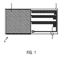
図1には、窒化アルミニウムまたは酸化アルミニウムから成るセラミック基板4の一部分が示されており、この基板には、大電力領域1と小電力領域2を含む金属被覆部が設けられている。図示されている金属被覆部はセラミック基板上で、大電力領域1において何度も同じように被着され、目標破断箇所3に沿って折ることにより個別に分離することができる。 FIG. 1 shows a part of a ceramic substrate 4 made of aluminum nitride or aluminum oxide, and this substrate is provided with a metal coating including a high power region 1 and a low power region 2. The illustrated metal coating can be applied in the same way over and over in the high power region 1 on the ceramic substrate and can be separated separately by folding along the target break 3.
セラミック基板上には、大電力領域1と小電力領域2が並置されて設けられている。ここで大電力領域1とは、その用途ゆえに大きい電流容量と高い熱伝導性を有する領域のことを意味する。大電力領域1には、動作中、著しく熱くなるデバイスおよび/または高い投入電力を有するデバイスたとえばLEDまたは制御トランジスタなどが取り付けられる。このようなデバイスの大きい電力と放出熱を流さなければならず、もしくは排出しなければならない。 On the ceramic substrate, a large power region 1 and a small power region 2 are provided side by side. Here, the high power region 1 means a region having a large current capacity and high thermal conductivity because of its use. The high power region 1 is fitted with devices that become very hot during operation and / or devices with high input power, such as LEDs or control transistors. The large power and heat released from such devices must be passed or discharged.
小電力領域2とは、熱放出を僅かなものとすることができる金属被覆部もしくは導体路のことである。これはたとえば、多くはロジック回路と呼ばれる回路における本来の導体路である。 The low power region 2 is a metal coating portion or a conductor path that can minimize heat release. This is, for example, an intrinsic conductor path in a circuit called a logic circuit.
本発明の1つの重要な特徴は、Rzが小さく(有利には5μm程度)波立った状態のない高い精度で水平な面を形成するために、大電力領域1が研磨プロセスにより平坦化されることにある。このようにするだけで、薄いはんだ層(有利には10μm程度)によっても電力用デバイスの熱を十分に放出させることができる。 One important feature of the present invention is that the high power region 1 is flattened by a polishing process in order to form a horizontal surface with high precision with a small R z (preferably around 5 μm) and no wavy state. There is to be. By only doing so, the heat of the power device can be sufficiently released even by a thin solder layer (advantageously about 10 μm).
Claims (8)
マルチレベル金属被覆部を製造する方法において、
以下のステップを以下の順序で実施する、すなわち、
e)ガラスを含有する銅ベースペーストから成る、前記大電力領域(1)と前記小電力領域(2)のための共通のベース金属被覆部を、スクリーン印刷またはタンポ印刷によって20〜50μmの厚さで印刷するステップと、
f)ガラス成分のない銅補強ペーストを、銅の厚さ全体が300〜500μmになるまでスクリーン印刷またはステンシル印刷によって複数回または多数回、前記ベース金属被覆部に印刷することにより、前記大電力領域(1)において前記ベース金属被覆部を補強するステップと、
g)金属被覆された前記セラミック基板(4)を、前記大電力領域(1)および前記小電力領域(2)と共に窒素中において850〜950℃で焼成するステップと、
h)前記大電力領域(1)を機械的に平坦化して、粗さRz<5μmの平坦な表面を形成するステップと、
を実施することを特徴とする、
マルチレベル金属被覆部を製造する方法。 A ceramic substrate (4) made of AlN or Al 2 O 3, a method for producing a multi-level metallization comprising copper, to one and the same ceramic substrate (4), with a metallization current capacity is large Forming a high power region (1) and a low power region (2) having a metal coating with a small current capacity;
In a method of manufacturing a multilevel metal coating,
The following steps are performed in the following order:
e) A common base metal coating for the high power region (1) and the low power region (2), made of glass-containing copper base paste, with a thickness of 20-50 μm by screen printing or tampo printing. Printing with
f) The high power region is obtained by printing the copper reinforcing paste having no glass component on the base metal coating part by screen printing or stencil printing several times or many times until the total thickness of copper becomes 300 to 500 μm. Reinforcing the base metal covering in (1);
g) firing the metal coated ceramic substrate (4) together with the high power region (1) and the low power region (2) in nitrogen at 850-950 ° C .;
h) mechanically planarizing the high power region (1) to form a flat surface with a roughness R z <5 μm;
It is characterized by carrying out
A method for producing a multi-level metal coating.
請求項1記載の方法。 After the planarization, a metal coating such as Ni, NiP + Pd + Au, Ag or Ni + Au is provided electrolessly in the high power region (1) and / or the low power region (2).
The method of claim 1.
請求項1または2記載の方法。 As a preparation for later separating the ceramic substrate (4) into individual partial substrates, the ceramic substrate (4) is processed by a laser scribe (3) before or after printing,
The method according to claim 1 or 2.
請求項1から3のいずれか1項記載の方法。 In the planarization, grinding of 100 to 150 μm is performed.
4. A method according to any one of claims 1 to 3.
請求項1から4のいずれか1項記載の方法。 The proportion of glass in the copper base paste containing glass is 4-8%, preferably 6%.
5. A method according to any one of claims 1 to 4.
請求項1から5のいずれか1項記載の方法。 After the planarization, the thickness of the metal covering portion of the high power region (1) is 180 to 220 μm.
6. A method according to any one of claims 1-5.
銅から成るマルチレベル金属被覆部が設けられており、該マルチレベル金属被覆部は、電流容量が大きい金属被覆部を有する大電力領域(1)と、電流容量が小さい金属被覆部を有する小電力領域(2)とを備えている、
セラミック基板(4)において、
前記金属被覆部の厚さは、前記大電力領域(1)では180〜220μmであり、前記小電力領域(2)では20〜50μmであり、前記金属被覆部の付着力は、60N/qmmを超えた付近にあることを特徴とする、
セラミック基板。 A ceramic substrate (4) made of AlN or Al 2 O 3 , produced by the method according to claim 1,
A multi-level metal cover made of copper is provided, the multi-level metal cover being a high power region (1) having a metal cover with a large current capacity and a low power having a metal cover with a small current capacity. A region (2),
In the ceramic substrate (4),
The thickness of the metal coating portion is 180 to 220 μm in the high power region (1) and 20 to 50 μm in the low power region (2), and the adhesion force of the metal coating portion is 60 N / qmm. It is characterized by being in the vicinity,
Ceramic substrate.
請求項7記載のセラミック基板。 The edge gradient of the metal covering portion of the high power region (1) is in the vicinity of 120 μm if the entire copper thickness is 200 μm.
The ceramic substrate according to claim 7.
Applications Claiming Priority (3)
| Application Number | Priority Date | Filing Date | Title |
|---|---|---|---|
| DE102013202008 | 2013-02-07 | ||
| DE102013202008.2 | 2013-02-07 | ||
| PCT/EP2014/052177 WO2014122137A1 (en) | 2013-02-07 | 2014-02-05 | Multi-level metalization on a ceramic substrate |
Publications (1)
| Publication Number | Publication Date |
|---|---|
| JP2016507902A true JP2016507902A (en) | 2016-03-10 |
Family
ID=50280346
Family Applications (1)
| Application Number | Title | Priority Date | Filing Date |
|---|---|---|---|
| JP2015556472A Pending JP2016507902A (en) | 2013-02-07 | 2014-02-05 | Multi-level metal coating on the ceramic substrate |
Country Status (9)
| Country | Link |
|---|---|
| US (2) | US20150366075A1 (en) |
| EP (1) | EP2954554B1 (en) |
| JP (1) | JP2016507902A (en) |
| CN (1) | CN105074913B (en) |
| DE (1) | DE102014202007A1 (en) |
| ES (1) | ES2630371T3 (en) |
| PH (1) | PH12015501631A1 (en) |
| TW (1) | TWI636716B (en) |
| WO (1) | WO2014122137A1 (en) |
Cited By (1)
| Publication number | Priority date | Publication date | Assignee | Title |
|---|---|---|---|---|
| WO2022162875A1 (en) * | 2021-01-29 | 2022-08-04 | サンケン電気株式会社 | Semiconductor power module |
Families Citing this family (2)
| Publication number | Priority date | Publication date | Assignee | Title |
|---|---|---|---|---|
| CN108735707B (en) * | 2018-04-18 | 2020-11-06 | 华为技术有限公司 | Ceramic substrate, preparation method of ceramic substrate and power module |
| DE102018127075B4 (en) | 2018-10-30 | 2021-12-30 | Auto-Kabel Management Gmbh | High current circuit |
Citations (11)
| Publication number | Priority date | Publication date | Assignee | Title |
|---|---|---|---|---|
| JPS59167094A (en) * | 1983-03-12 | 1984-09-20 | 松下電工株式会社 | Method of producing circuit board |
| JPS62278702A (en) * | 1986-05-28 | 1987-12-03 | 富士通株式会社 | Conducting paste |
| JPH08298359A (en) * | 1995-04-26 | 1996-11-12 | Kyocera Corp | Thick copper film circuit board |
| JP2001353716A (en) * | 2000-06-13 | 2001-12-25 | Murata Mfg Co Ltd | Method for forming break groove onto ceramic aggregate substrate |
| JP2004172182A (en) * | 2002-11-18 | 2004-06-17 | Denki Kagaku Kogyo Kk | Circuit board and its manufacturing method |
| JP2007180399A (en) * | 2005-12-28 | 2007-07-12 | Dowa Holdings Co Ltd | Metal-ceramics circuit board and manufacturing method thereof |
| JP2007201346A (en) * | 2006-01-30 | 2007-08-09 | Mitsuboshi Belting Ltd | Ceramics circuit board and its manufacturing method |
| WO2008081758A1 (en) * | 2006-12-28 | 2008-07-10 | Tokuyama Corporation | Process for producing metallized aluminum nitride substrate |
| JP2010050164A (en) * | 2008-08-19 | 2010-03-04 | Mitsubishi Materials Corp | Method of manufacturing board for power module |
| JP2011216533A (en) * | 2010-03-31 | 2011-10-27 | Dowa Metaltech Kk | Metal ceramic joined circuit board and method of manufacturing the same |
| JP2012142318A (en) * | 2010-12-28 | 2012-07-26 | Mitsuboshi Belting Ltd | Manufacturing method of pattern substrate |
Family Cites Families (15)
| Publication number | Priority date | Publication date | Assignee | Title |
|---|---|---|---|---|
| US3074143A (en) * | 1960-02-01 | 1963-01-22 | Baynard R Smith | Method of making metalized ceramic bodies |
| US3504223A (en) * | 1967-09-07 | 1970-03-31 | Litton Precision Prod Inc | High power wide band cross field amplifier with ceramic supported helix |
| US3809797A (en) * | 1971-11-16 | 1974-05-07 | Du Pont | Seal ring compositions and electronic packages made therewith |
| US5156903A (en) * | 1989-12-21 | 1992-10-20 | Sumitomo Metal Ceramics Inc. | Multilayer ceramic substrate and manufacture thereof |
| US5126206A (en) * | 1990-03-20 | 1992-06-30 | Diamonex, Incorporated | Diamond-on-a-substrate for electronic applications |
| US5202153A (en) | 1991-08-23 | 1993-04-13 | E. I. Du Pont De Nemours And Company | Method for making thick film/solder joints |
| JPH0897553A (en) * | 1994-09-21 | 1996-04-12 | Toyo Commun Equip Co Ltd | Structure for conductive pattern |
| US5736456A (en) * | 1996-03-07 | 1998-04-07 | Micron Technology, Inc. | Method of forming conductive bumps on die for flip chip applications |
| JP3315649B2 (en) | 1998-08-11 | 2002-08-19 | 富士通株式会社 | Electronics |
| US7239219B2 (en) * | 2001-12-03 | 2007-07-03 | Microfabrica Inc. | Miniature RF and microwave components and methods for fabricating such components |
| EP1898476B1 (en) * | 2005-06-15 | 2014-11-19 | Kyocera Corporation | Multilayer piezoelectric element and ejector using this |
| KR101391924B1 (en) * | 2007-01-05 | 2014-05-07 | 페어차일드코리아반도체 주식회사 | Semiconductor package |
| TWI396492B (en) * | 2007-09-25 | 2013-05-11 | Ngk Spark Plug Co | Method for manufacturing wire substrate |
| DE102009000491B4 (en) * | 2009-01-29 | 2017-02-16 | Fraunhofer-Gesellschaft zur Förderung der angewandten Forschung e.V. | Metallized, hermetic vias and methods of making the same |
| CN102850091B (en) * | 2011-06-28 | 2014-04-30 | 比亚迪股份有限公司 | Ceramic surface selective metallization method and ceramic |
-
2014
- 2014-02-05 JP JP2015556472A patent/JP2016507902A/en active Pending
- 2014-02-05 WO PCT/EP2014/052177 patent/WO2014122137A1/en active Application Filing
- 2014-02-05 US US14/763,694 patent/US20150366075A1/en not_active Abandoned
- 2014-02-05 EP EP14710196.8A patent/EP2954554B1/en active Active
- 2014-02-05 CN CN201480007836.2A patent/CN105074913B/en active Active
- 2014-02-05 DE DE102014202007.7A patent/DE102014202007A1/en not_active Withdrawn
- 2014-02-05 ES ES14710196.8T patent/ES2630371T3/en active Active
- 2014-02-06 TW TW103103864A patent/TWI636716B/en active
-
2015
- 2015-07-23 PH PH12015501631A patent/PH12015501631A1/en unknown
-
2017
- 2017-06-20 US US15/627,703 patent/US10568214B2/en active Active
Patent Citations (11)
| Publication number | Priority date | Publication date | Assignee | Title |
|---|---|---|---|---|
| JPS59167094A (en) * | 1983-03-12 | 1984-09-20 | 松下電工株式会社 | Method of producing circuit board |
| JPS62278702A (en) * | 1986-05-28 | 1987-12-03 | 富士通株式会社 | Conducting paste |
| JPH08298359A (en) * | 1995-04-26 | 1996-11-12 | Kyocera Corp | Thick copper film circuit board |
| JP2001353716A (en) * | 2000-06-13 | 2001-12-25 | Murata Mfg Co Ltd | Method for forming break groove onto ceramic aggregate substrate |
| JP2004172182A (en) * | 2002-11-18 | 2004-06-17 | Denki Kagaku Kogyo Kk | Circuit board and its manufacturing method |
| JP2007180399A (en) * | 2005-12-28 | 2007-07-12 | Dowa Holdings Co Ltd | Metal-ceramics circuit board and manufacturing method thereof |
| JP2007201346A (en) * | 2006-01-30 | 2007-08-09 | Mitsuboshi Belting Ltd | Ceramics circuit board and its manufacturing method |
| WO2008081758A1 (en) * | 2006-12-28 | 2008-07-10 | Tokuyama Corporation | Process for producing metallized aluminum nitride substrate |
| JP2010050164A (en) * | 2008-08-19 | 2010-03-04 | Mitsubishi Materials Corp | Method of manufacturing board for power module |
| JP2011216533A (en) * | 2010-03-31 | 2011-10-27 | Dowa Metaltech Kk | Metal ceramic joined circuit board and method of manufacturing the same |
| JP2012142318A (en) * | 2010-12-28 | 2012-07-26 | Mitsuboshi Belting Ltd | Manufacturing method of pattern substrate |
Cited By (1)
| Publication number | Priority date | Publication date | Assignee | Title |
|---|---|---|---|---|
| WO2022162875A1 (en) * | 2021-01-29 | 2022-08-04 | サンケン電気株式会社 | Semiconductor power module |
Also Published As
| Publication number | Publication date |
|---|---|
| US20170290169A1 (en) | 2017-10-05 |
| US20150366075A1 (en) | 2015-12-17 |
| DE102014202007A1 (en) | 2014-08-07 |
| PH12015501631B1 (en) | 2015-10-19 |
| US10568214B2 (en) | 2020-02-18 |
| ES2630371T3 (en) | 2017-08-21 |
| TWI636716B (en) | 2018-09-21 |
| EP2954554B1 (en) | 2017-04-12 |
| WO2014122137A1 (en) | 2014-08-14 |
| EP2954554A1 (en) | 2015-12-16 |
| CN105074913B (en) | 2018-05-22 |
| TW201442582A (en) | 2014-11-01 |
| PH12015501631A1 (en) | 2015-10-19 |
| CN105074913A (en) | 2015-11-18 |
Similar Documents
| Publication | Publication Date | Title |
|---|---|---|
| RU2014148797A (en) | PCB, IN PARTICULAR, FOR A HIGH-CURRENT ELECTRONIC MODULE CONTAINING AN ELECTRIC-CONDUCTING SUBSTRATE | |
| JP4819150B2 (en) | Method for forming electrode pattern on ceramic substrate | |
| US10568214B2 (en) | Method for producing multi-level metalization on a ceramic substrate | |
| KR20180093877A (en) | Ceramic paste bonded with a metal or metal hybrid foil | |
| US9232645B2 (en) | High speed differential wiring in glass ceramic MCMS | |
| JP5145036B2 (en) | Method for forming ceramic conductor board | |
| JP4564820B2 (en) | Multi-piece wiring board and manufacturing method thereof | |
| JP2007173586A (en) | Wiring mother board provided with a plurality of wiring patterns, and inspecting method therefor | |
| KR20110116819A (en) | Printed circuit substrate and method of manufacturing the same | |
| JPH0575255A (en) | Hybrid substrate and circuit module on which the substrate is mounted, and manufacture thereof | |
| US7383630B2 (en) | Method for making a circuit plate | |
| JPH04208591A (en) | Ceramic printed circuit board | |
| KR101116134B1 (en) | Board for led package and method of manufacture the same | |
| JP2015106570A (en) | Multi-piece wiring board, wiring board and electronic apparatus | |
| JP2013175659A (en) | Multiple patterning wiring board | |
| JP4738220B2 (en) | Multiple wiring board | |
| JP2010183117A (en) | Multiple patterning wiring board, and method of manufacturing the same | |
| KR20170040657A (en) | Ceramic Board For Power Module | |
| JP6282959B2 (en) | Multi-cavity wiring board, wiring board and electronic device | |
| CN103426993A (en) | Electronic module, illuminating device and method for manufacturing electronic module | |
| JP2004080063A (en) | High-reliability substrate for semiconductor | |
| KR20200096285A (en) | Method for forming thermally conductive connections between power components and metal layers of circuit carriers | |
| JPH0763109B2 (en) | Ceramic circuit board manufacturing method | |
| JPS62119951A (en) | Multilayer interconnection substrate | |
| JP2005072510A (en) | Multiple patterning wiring board |
Legal Events
| Date | Code | Title | Description |
|---|---|---|---|
| A621 | Written request for application examination |
Free format text: JAPANESE INTERMEDIATE CODE: A621 Effective date: 20170202 |
|
| A977 | Report on retrieval |
Free format text: JAPANESE INTERMEDIATE CODE: A971007 Effective date: 20180213 |
|
| A131 | Notification of reasons for refusal |
Free format text: JAPANESE INTERMEDIATE CODE: A131 Effective date: 20180226 |
|
| A601 | Written request for extension of time |
Free format text: JAPANESE INTERMEDIATE CODE: A601 Effective date: 20180528 |
|
| A131 | Notification of reasons for refusal |
Free format text: JAPANESE INTERMEDIATE CODE: A131 Effective date: 20181210 |
|
| A601 | Written request for extension of time |
Free format text: JAPANESE INTERMEDIATE CODE: A601 Effective date: 20190308 |
|
| A02 | Decision of refusal |
Free format text: JAPANESE INTERMEDIATE CODE: A02 Effective date: 20190701 |