JP2016134329A - Light-emitting device - Google Patents
Light-emitting device Download PDFInfo
- Publication number
- JP2016134329A JP2016134329A JP2015009167A JP2015009167A JP2016134329A JP 2016134329 A JP2016134329 A JP 2016134329A JP 2015009167 A JP2015009167 A JP 2015009167A JP 2015009167 A JP2015009167 A JP 2015009167A JP 2016134329 A JP2016134329 A JP 2016134329A
- Authority
- JP
- Japan
- Prior art keywords
- emitting device
- insulating layer
- electrode
- light emitting
- light
- Prior art date
- Legal status (The legal status is an assumption and is not a legal conclusion. Google has not performed a legal analysis and makes no representation as to the accuracy of the status listed.)
- Pending
Links
- 239000010410 layer Substances 0.000 claims abstract description 82
- 239000000463 material Substances 0.000 claims abstract description 42
- 239000002245 particle Substances 0.000 claims abstract description 39
- 239000000758 substrate Substances 0.000 claims abstract description 33
- 238000000576 coating method Methods 0.000 claims abstract description 27
- 239000011248 coating agent Substances 0.000 claims abstract description 23
- 239000012044 organic layer Substances 0.000 claims abstract description 20
- XLYOFNOQVPJJNP-UHFFFAOYSA-N water Substances O XLYOFNOQVPJJNP-UHFFFAOYSA-N 0.000 claims description 3
- 239000002344 surface layer Substances 0.000 claims description 2
- 238000009413 insulation Methods 0.000 abstract 3
- 238000000034 method Methods 0.000 description 11
- 238000007789 sealing Methods 0.000 description 10
- 230000004048 modification Effects 0.000 description 7
- 238000012986 modification Methods 0.000 description 7
- 239000011347 resin Substances 0.000 description 6
- 229920005989 resin Polymers 0.000 description 6
- 229910052751 metal Inorganic materials 0.000 description 5
- 239000002184 metal Substances 0.000 description 5
- XLOMVQKBTHCTTD-UHFFFAOYSA-N Zinc monoxide Chemical compound [Zn]=O XLOMVQKBTHCTTD-UHFFFAOYSA-N 0.000 description 4
- 238000003892 spreading Methods 0.000 description 4
- 238000002347 injection Methods 0.000 description 3
- 239000007924 injection Substances 0.000 description 3
- 239000011368 organic material Substances 0.000 description 3
- 238000004544 sputter deposition Methods 0.000 description 3
- 238000007740 vapor deposition Methods 0.000 description 3
- 239000004695 Polyether sulfone Substances 0.000 description 2
- 239000004642 Polyimide Substances 0.000 description 2
- 230000004888 barrier function Effects 0.000 description 2
- 239000002274 desiccant Substances 0.000 description 2
- 239000000945 filler Substances 0.000 description 2
- 239000011521 glass Substances 0.000 description 2
- 238000005192 partition Methods 0.000 description 2
- 229920003207 poly(ethylene-2,6-naphthalate) Polymers 0.000 description 2
- 229920006393 polyether sulfone Polymers 0.000 description 2
- -1 polyethylene naphthalate Polymers 0.000 description 2
- 239000011112 polyethylene naphthalate Substances 0.000 description 2
- 229920000139 polyethylene terephthalate Polymers 0.000 description 2
- 239000005020 polyethylene terephthalate Substances 0.000 description 2
- 229920001721 polyimide Polymers 0.000 description 2
- 239000005871 repellent Substances 0.000 description 2
- 229910052814 silicon oxide Inorganic materials 0.000 description 2
- 239000011787 zinc oxide Substances 0.000 description 2
- OKTJSMMVPCPJKN-UHFFFAOYSA-N Carbon Chemical compound [C] OKTJSMMVPCPJKN-UHFFFAOYSA-N 0.000 description 1
- 229920001609 Poly(3,4-ethylenedioxythiophene) Polymers 0.000 description 1
- 239000004793 Polystyrene Substances 0.000 description 1
- 229910052581 Si3N4 Inorganic materials 0.000 description 1
- VYPSYNLAJGMNEJ-UHFFFAOYSA-N Silicium dioxide Chemical compound O=[Si]=O VYPSYNLAJGMNEJ-UHFFFAOYSA-N 0.000 description 1
- BSUHXFDAHXCSQL-UHFFFAOYSA-N [Zn+2].[W+4].[O-2].[In+3] Chemical compound [Zn+2].[W+4].[O-2].[In+3] BSUHXFDAHXCSQL-UHFFFAOYSA-N 0.000 description 1
- 239000000853 adhesive Substances 0.000 description 1
- 230000001070 adhesive effect Effects 0.000 description 1
- 239000000956 alloy Substances 0.000 description 1
- 229910045601 alloy Inorganic materials 0.000 description 1
- 229910052782 aluminium Inorganic materials 0.000 description 1
- 239000002041 carbon nanotube Substances 0.000 description 1
- 229910021393 carbon nanotube Inorganic materials 0.000 description 1
- 238000005229 chemical vapour deposition Methods 0.000 description 1
- 239000011247 coating layer Substances 0.000 description 1
- 238000010586 diagram Methods 0.000 description 1
- 229910052737 gold Inorganic materials 0.000 description 1
- 230000005525 hole transport Effects 0.000 description 1
- 229910052738 indium Inorganic materials 0.000 description 1
- AMGQUBHHOARCQH-UHFFFAOYSA-N indium;oxotin Chemical compound [In].[Sn]=O AMGQUBHHOARCQH-UHFFFAOYSA-N 0.000 description 1
- 239000011810 insulating material Substances 0.000 description 1
- 229910052749 magnesium Inorganic materials 0.000 description 1
- 238000004519 manufacturing process Methods 0.000 description 1
- 229910044991 metal oxide Inorganic materials 0.000 description 1
- 150000004706 metal oxides Chemical class 0.000 description 1
- 230000003287 optical effect Effects 0.000 description 1
- TWNQGVIAIRXVLR-UHFFFAOYSA-N oxo(oxoalumanyloxy)alumane Chemical compound O=[Al]O[Al]=O TWNQGVIAIRXVLR-UHFFFAOYSA-N 0.000 description 1
- RVTZCBVAJQQJTK-UHFFFAOYSA-N oxygen(2-);zirconium(4+) Chemical compound [O-2].[O-2].[Zr+4] RVTZCBVAJQQJTK-UHFFFAOYSA-N 0.000 description 1
- 229910052697 platinum Inorganic materials 0.000 description 1
- 229920000642 polymer Polymers 0.000 description 1
- 229920002223 polystyrene Polymers 0.000 description 1
- HQVNEWCFYHHQES-UHFFFAOYSA-N silicon nitride Chemical compound N12[Si]34N5[Si]62N3[Si]51N64 HQVNEWCFYHHQES-UHFFFAOYSA-N 0.000 description 1
- 229910052709 silver Inorganic materials 0.000 description 1
- 238000000638 solvent extraction Methods 0.000 description 1
- 239000007921 spray Substances 0.000 description 1
- 230000001629 suppression Effects 0.000 description 1
- 230000003746 surface roughness Effects 0.000 description 1
- 229910052718 tin Inorganic materials 0.000 description 1
- 238000001039 wet etching Methods 0.000 description 1
- 229910052725 zinc Inorganic materials 0.000 description 1
- 239000011701 zinc Substances 0.000 description 1
- YVTHLONGBIQYBO-UHFFFAOYSA-N zinc indium(3+) oxygen(2-) Chemical compound [O--].[Zn++].[In+3] YVTHLONGBIQYBO-UHFFFAOYSA-N 0.000 description 1
- 229910001928 zirconium oxide Inorganic materials 0.000 description 1
Images


Abstract
Description
本発明は、発光装置に関する。 The present invention relates to a light emitting device.
有機EL素子を光源として利用した発光装置の開発が進んでいる。有機EL素子は、有機層を第1電極と第2電極とで挟んだ構成を有している。このような発光装置は、有機EL素子に電気的に接続する端子を有している。 Development of a light emitting device using an organic EL element as a light source is in progress. The organic EL element has a configuration in which an organic layer is sandwiched between a first electrode and a second electrode. Such a light emitting device has a terminal that is electrically connected to the organic EL element.
一方、有機EL素子を有する発光装置では、有機層と第1電極が接する領域を定めるために、絶縁層が形成されている。 On the other hand, in a light emitting device having an organic EL element, an insulating layer is formed to define a region where the organic layer and the first electrode are in contact.
なお、特許文献1には、有機EL素子を画素に用いた発光装置において、画素を区画するための絶縁性の隔壁に、絶縁性のフィラーを混入させることが記載されている。特許文献1によれば、フィラーを混ぜることにより、隔壁の表面粗さRaを0.05μm以上1.0μm以下にすることができ、その結果、発光層を塗布材料で形成する際に、隣の画素に発光層が混ざることを抑制できる。
Note that
有機層の少なくとも一部の層を塗布法で形成する場合、塗布された有機材料が、上記した絶縁層の外側に広がり、発光装置の端子が有機材料で覆われる可能性が出てくる。この場合、端子とこの端子に接続すべき導通部材の間で接続不良が発生する可能性が出てくる。 When at least a part of the organic layer is formed by a coating method, the applied organic material spreads outside the above-described insulating layer, and the terminal of the light-emitting device may be covered with the organic material. In this case, there is a possibility that a connection failure occurs between the terminal and the conductive member to be connected to the terminal.
本発明が解決しようとする課題としては、発光装置の有機層を塗布材料で形成する場合において、塗布材料が発光装置の端子まで広がらないようにすることが一例として挙げられる。 An example of a problem to be solved by the present invention is to prevent the coating material from spreading to the terminals of the light emitting device when the organic layer of the light emitting device is formed of the coating material.
請求項1に記載の発明は、基板と、
前記基板に形成され、有機層を有する発光部と、
前記発光部に電気的に接続する端子と、
少なくとも前記発光部と前記端子の間に位置し、絶縁性の粒子を含む絶縁層と、
を備え、
前記絶縁層の上面は凹凸を有している発光装置である。
The invention according to
A light emitting part formed on the substrate and having an organic layer;
A terminal electrically connected to the light emitting unit;
An insulating layer located at least between the light emitting portion and the terminal and containing insulating particles;
With
The upper surface of the insulating layer is a light emitting device having irregularities.
以下、本発明の実施の形態について、図面を用いて説明する。尚、すべての図面において、同様な構成要素には同様の符号を付し、適宜説明を省略する。 Hereinafter, embodiments of the present invention will be described with reference to the drawings. In all the drawings, the same reference numerals are given to the same components, and the description will be omitted as appropriate.
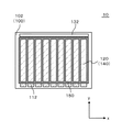
図1は、実施形態に係る発光装置10の構成を示す平面図である。図2は、図1から第2電極130を取り除いた図である。図3は図1のA−A断面を示している。図4は、図3の点線αで囲んだ領域を拡大した図である。ただし図4において、第2電極130は省略されている。また、封止部材160は、図3にのみ図示されている。
FIG. 1 is a plan view showing a configuration of a
実施形態に係る発光装置10は、図1〜図3に示すように、基板100、発光部140、第1端子112(端子)、及び絶縁層150を有している。発光部140は基板100に形成されており、有機層を有している。第1端子112は発光部140に電気的に接続している。絶縁層150は、少なくとも発光部140と第1端子112の間に位置しており、図4に示すように絶縁性の粒子152を含んでいる。そして図4に示すように、絶縁層150の上面は凹凸を有している。本図に示す例において、発光装置10は照明装置である。このため、発光部140の面積は、基板100の面積の3/4倍以上1倍未満である。以下、詳細に説明する。
As illustrated in FIGS. 1 to 3, the
まず、図1〜図3を用いて、発光装置10の構成について説明する。
First, the configuration of the
発光装置10がボトムエミッション型の発光装置である場合、基板100は、例えばガラス基板や樹脂基板などの透光性を有する基板である。一方、発光装置10がトップエミッション型の発光装置である場合、基板100は透光性を有していなくてもよい。また、基板100は可撓性を有していてもよい。この場合、基板100が湾曲した状態で発光装置10を使用することができる。可撓性を有している場合、基板100の厚さは、例えば10μm以上1000μm以下である。基板100は、例えば矩形などの多角形である。基板100が樹脂基板である場合、基板100は、例えばPEN(ポリエチレンナフタレート)、PES(ポリエーテルサルホン)、PET(ポリエチレンテレフタラート)、又はポリイミドを用いて形成されている。また、基板100が樹脂基板である場合、水分が基板100を透過することを抑制するために、基板100の少なくとも一面(好ましくは両面)に、SiNxやSiONなどの無機バリア膜が形成されている。なお、この無機バリア膜と基板100の間に、平坦化層(例えば有機層)が設けられていてもよい。
When the
基板100の第1面102には、発光部140が設けられている。発光部140は、第1電極110、有機層120、及び第2電極130をこの順に積層させた構成を有している。
A
第1電極110は、光透過性を有する透明電極である。透明電極の材料は、金属を含む材料、例えば、ITO(Indium Tin Oxide)、IZO(Indium Zinc Oxide)、IWZO(Indium Tungsten Zinc Oxide)、ZnO(Zinc Oxide)等の金属酸化物である。第1電極110の厚さは、例えば10nm以上500nm以下である。第1電極110は、例えばスパッタリング法又は蒸着法を用いて形成される。なお、第1電極110は、カーボンナノチューブ、又はPEDOT/PSSなどの導電性有機材料であってもよい。
The
有機層120は発光層を有している。有機層120は、例えば、正孔注入層、発光層、及び電子注入層をこの順に積層させた構成を有している。正孔注入層と発光層との間には正孔輸送層が形成されていてもよい。有機層120のうち少なくとも一つの層、例えば第1電極110と接触する層は、インクジェット法、印刷法、又はスプレー法などの塗布法によって形成されてもよい。なお、この場合、有機層120の残りの層は、蒸着法によって形成されている。また、有機層120のすべての層が、塗布法を用いて形成されていてもよい。
The
第2電極130は、例えば、Al、Au、Ag、Pt、Mg、Sn、Zn、及びInからなる第1群の中から選択される金属、又はこの第1群から選択される金属の合金からなる金属層を含んでいる。この場合、第2電極130は遮光性を有している。第2電極130の厚さは、例えば10nm以上500nm以下である。ただし、第2電極130は、第1電極110の材料として例示した材料を用いて形成されていてもよい。第2電極130は、例えばスパッタリング法又は蒸着法を用いて形成される。
The
なお、上記した第1電極110及び第2電極130の材料は、発光装置10がボトムエミッション型の場合である。発光装置10がトップエミッション型の場合、第1電極110の材料と第2電極130の材料は逆になる。すなわち第1電極110の材料には上記した第2電極130の材料が用いられ、第2電極130の材料には上記した第1電極110の材料が用いられる。
Note that the materials of the
第1電極110の縁は、絶縁層150によって覆われている。絶縁層150は、第1電極110のうち発光部140となる領域を画定している。言い換えると、絶縁層150は発光部140を囲んでいる。そして絶縁層150の一部は、発光部140と第1端子112の間に位置している。絶縁層150は例えばポリイミドなどの感光性の樹脂材料によって形成されており、第1電極110のうち発光部140の発光領域となる部分を囲んでいる。絶縁層150を設けることにより、第1電極110の縁において第1電極110と第2電極130が短絡することを抑制できる。絶縁層150は、絶縁層150となる塗布材料を塗布した後、この塗布材料を露光及び現像することにより、形成される。
The edge of the
また、絶縁層150は複数の粒子152を含んでいる。粒子152の少なくとも表面は絶縁性である。粒子152は、例えば絶縁性の材料を用いて形成されている。粒子152を構成する材料は、例えば、酸化シリコン、窒化ケイ素、酸化アルミニウム、酸化ジルコニウム、またはポリスチレンなどの高分子である。また、粒子152の少なくとも表面は疎水性を有しているのが好ましい。特に粒子152の少なくとも表面は、絶縁層150と比較して疎水性が高いのが好ましい。このようにするためには、例えば、粒子152を構成する材料として撥水性の材料を選択してもよいし、粒子152の表面に撥水性のコーティング層を形成してもよい。粒子152の直径の平均値は、例えば100nm以上2000nm(2μm)以下である。特に絶縁層150の凹凸の大きさが、1〜3μmの間で形成されるのが好ましいため、粒子152が絶縁層150の下に位置する場合は、粒子152の直径はこの凹凸の大きさより小さいことが望ましい。
The insulating
本図に示す例において、粒子152は、絶縁層150となる塗布材料に予め含まれている。このため、粒子152は、絶縁層150の全体に分布している。また、一部の粒子152は、絶縁層150の表層に位置している。このため、絶縁層150の上面は、粒子152の有無に起因した凹凸が形成される。言い換えると、絶縁層150の上面の凸部の下方には、粒子152が位置している。なお、絶縁層150の上面において、粒子152は露出していてもよいし、絶縁層150の本体となる樹脂材料によって薄く覆われていてもよい。
In the example shown in this figure, the
また、発光装置10は、第1端子112及び第2端子132を有している。第1端子112は第1電極110に接続しており、第2端子132は第2電極130に接続している。第1端子112及び第2端子132は、例えば、第1電極110と同一の材料で形成された層を有している。また、第1端子112及び第2端子132の少なくとも一つの少なくとも一部は、この層の上に、第1電極110よりも低抵抗な金属膜を有していてもよい。第1端子112及び第2端子132のうち第1電極110と同一の材料で形成された層は、第1電極110と同一工程で形成されている。このため、第1電極110は、第1端子112の少なくとも一部の層と一体になっている。なお、第1端子112と第1電極110の間には引出配線が設けられていてもよい。また、第2端子132と第2電極130の間にも引出配線が設けられていてもよい。
In addition, the
第1端子112には、ボンディングワイヤ又はリード端子などの導電部材を介して制御回路の正極端子が接続され、第2端子132には、ボンディングワイヤ又はリード端子などの導電部材を介して制御回路の負極端子が接続される。
The positive terminal of the control circuit is connected to the
さらに図3に示すように、発光装置10は封止部材160を有している。封止部材160は透光性を有しており、例えばガラス又は樹脂を用いて形成されている。封止部材160は、基板100と同様の多角形や円形であり、中央に凹部を設けた形状を有している。そして封止部材160の縁は接着材で基板100に固定されている。これにより、封止部材160と基板100で囲まれた空間は封止される。そして発光部140は、封止された空間の中に位置している。なお、封止部材160はALD法で形成された膜又はCVD法で形成された膜であってもよい。
Further, as shown in FIG. 3, the
また、発光装置10は、さらに乾燥剤を有していてもよい。乾燥剤は、例えば封止部材160によって封止された空間内、例えば封止部材160のうち基板100に対向する面に配置されている。
The
なお、本図に示す例において、発光装置10は発光部140を一つのみ有している。ただし、図5に示すように、発光部140は、第1端子112と第2端子132を結んだ直線に交わる方向(具体的にはx方向)において、複数に分割されていてもよい。この場合、第1端子112及び第1電極110は、発光部140別に設けられている。なお、図5においては、第2端子132及び第2電極130は、複数の発光部140に共通である。ただし、第2端子132及び第2電極130も、発光部140別に設けられていてもよい。
In the example shown in the drawing, the
次に、発光装置10の製造方法について説明する。まず、基板100に第1電極110を、例えばスパッタリング法を用いて形成する。この時、マスクを用いたりウェットエッチングを用いるなどして、第1電極110を所定のパターンにする。
Next, a method for manufacturing the
次いで、第1電極110の縁の上に絶縁層150となる塗布材料を塗布する。この際、この塗布材料は、粒子152を含んでいる。次いで、この塗布材料を硬化させる。これにより、絶縁層150は形成される。なお、絶縁層150が感光性の材料によって形成されている場合、絶縁層150となる塗布材料は、第1電極110の縁以外の領域にも塗布される。その後、露光工程及び現像工程が行われることにより、絶縁層150は、第1電極110の縁に形成される。またこの工程において、絶縁層150の上面には、粒子152の有無に起因した凹凸が形成される。具体的には、絶縁層150の上面のうち、下方に粒子152が存在している領域は、他の領域と比較して凸になる。
Next, a coating material to be the insulating
次いで、有機層120を形成する。有機層120のうちインクジェット法などの塗布法で形成される層は、第1電極110のうち絶縁層150で囲まれた領域内に塗布材料を位置させることにより、形成される。この際、塗布材料が絶縁層150の側面を這い上がって絶縁層150の上面に濡れ広がる可能性がある。これに対して本実施形態では、絶縁層150の上面には凹凸が形成されている。このため、塗布材料は絶縁層150の上面を乗り越えにくくなる。従って、塗布材料が、絶縁層150で囲まれた領域の外側に濡れ広がることを抑制できる。特に粒子152の直径が小さい場合、絶縁層150の表面の凹凸の周期は短くなるため、塗布材料が絶縁層150で囲まれた領域の外側に濡れ広がることをさらに抑制できる。
Next, the
また、粒子152の表面が撥水性を有しており、かつ絶縁層150の上面において粒子152が露出している場合、塗布材料が、絶縁層150で囲まれた領域の外側に濡れ広がることをさらに抑制できる。
In addition, when the surface of the
次いで、第2電極130を形成する。第2電極130も、例えばマスクを用いるなどして所定のパターンに形成される。その後、封止部材160を用いて発光部140を封止する。
Next, the
以上、本実施形態によれば、絶縁層150には粒子152が含まれている。このため、絶縁層150の上面には、粒子152の有無に起因した凹凸が形成される。従って、塗布材料が、絶縁層150で囲まれた領域の外側に濡れ広がることを抑制できる。粒子152の表面が撥水性を有しており、かつ絶縁層150の上面において粒子152が露出している場合、有機層120となる塗布材料は、特に濡れ広がりにくい。
As described above, according to the present embodiment, the insulating
(変形例)
図6は、変形例に係る発光装置10の構成を示す断面図であり、実施形態における図4に対応している。本変形例に係る発光装置10は、粒子152が絶縁層150の上層にのみ位置している点を除いて、実施形態に係る発光装置10と同様の構成である。
(Modification)
FIG. 6 is a cross-sectional view illustrating a configuration of a
本変形例において、絶縁層150となる塗布材料は、粒子152を含んでいない。その代わりに、粒子152は、絶縁層150の表面に配置されている。このようにするためには、例えば、粒子152を含む塗布材料を、絶縁層150の上に塗布すればよい。
In this modification, the coating material that becomes the
本変形例によっても、実施例と同様に、絶縁層150の上面には、粒子152の有無に起因した凹凸が形成される。従って、塗布材料が、絶縁層150で囲まれた領域の外側に濡れ広がることを抑制できる。
Also in the present modification, as in the embodiment, irregularities due to the presence or absence of the
以上、図面を参照して実施形態及び実施例について述べたが、これらは本発明の例示であり、上記以外の様々な構成を採用することもできる。 As mentioned above, although embodiment and the Example were described with reference to drawings, these are illustrations of this invention and can also employ | adopt various structures other than the above.
10 発光装置
100 基板
110 第1電極
112 第1端子
120 有機層
130 第2電極
132 第2端子
140 発光部
150 絶縁層
152 粒子
10 light emitting
Claims (6)
前記基板に形成され、有機層を有する発光部と、
前記発光部に電気的に接続する端子と、
少なくとも前記発光部と前記端子の間に位置し、絶縁性の粒子を含む絶縁層と、
を備え、
前記絶縁層の上面は凹凸を有している発光装置。 A substrate,
A light emitting part formed on the substrate and having an organic layer;
A terminal electrically connected to the light emitting unit;
An insulating layer located at least between the light emitting portion and the terminal and containing insulating particles;
With
A light-emitting device in which an upper surface of the insulating layer has irregularities.
前記絶縁層は前記発光部を囲んでいる発光装置。 The light-emitting device according to claim 1.
The insulating layer surrounds the light emitting unit.
前記発光装置は、少なくとも第1の方向において前記発光部を一つ有している発光装置。 The light-emitting device according to claim 1 or 2,
The light-emitting device has one light-emitting portion in at least the first direction.
前記粒子の少なくとも表面は撥水性を有している発光装置。 In the light-emitting device as described in any one of Claims 1-3,
A light-emitting device in which at least the surface of the particles has water repellency.
前記絶縁層は、塗布材料を用いて形成されている発光装置。 The light-emitting device according to claim 4.
The said insulating layer is a light-emitting device formed using the coating material.
前記粒子は、少なくとも前記絶縁層の表層に位置している発光装置。 In the light-emitting device as described in any one of Claims 1-5,
The light emitting device, wherein the particles are located at least on a surface layer of the insulating layer.
Priority Applications (1)
| Application Number | Priority Date | Filing Date | Title |
|---|---|---|---|
| JP2015009167A JP2016134329A (en) | 2015-01-21 | 2015-01-21 | Light-emitting device |
Applications Claiming Priority (1)
| Application Number | Priority Date | Filing Date | Title |
|---|---|---|---|
| JP2015009167A JP2016134329A (en) | 2015-01-21 | 2015-01-21 | Light-emitting device |
Publications (2)
| Publication Number | Publication Date |
|---|---|
| JP2016134329A true JP2016134329A (en) | 2016-07-25 |
| JP2016134329A5 JP2016134329A5 (en) | 2017-12-28 |
Family
ID=56464485
Family Applications (1)
| Application Number | Title | Priority Date | Filing Date |
|---|---|---|---|
| JP2015009167A Pending JP2016134329A (en) | 2015-01-21 | 2015-01-21 | Light-emitting device |
Country Status (1)
| Country | Link |
|---|---|
| JP (1) | JP2016134329A (en) |
Citations (4)
| Publication number | Priority date | Publication date | Assignee | Title |
|---|---|---|---|---|
| JP2002006129A (en) * | 2000-06-19 | 2002-01-09 | Canon Inc | Optical element and method for producing the same, liquid crystal device |
| JP2007095608A (en) * | 2005-09-30 | 2007-04-12 | Seiko Epson Corp | Electrooptical device, electronic apparatus and method of manufacturing electrooptical device |
| JP2010212177A (en) * | 2009-03-12 | 2010-09-24 | Toppan Printing Co Ltd | Organic el light emitting element and method of manufacturing the same |
| JP2014207199A (en) * | 2013-04-16 | 2014-10-30 | パイオニア株式会社 | Light-emitting element and method of manufacturing light-emitting element |
-
2015
- 2015-01-21 JP JP2015009167A patent/JP2016134329A/en active Pending
Patent Citations (4)
| Publication number | Priority date | Publication date | Assignee | Title |
|---|---|---|---|---|
| JP2002006129A (en) * | 2000-06-19 | 2002-01-09 | Canon Inc | Optical element and method for producing the same, liquid crystal device |
| JP2007095608A (en) * | 2005-09-30 | 2007-04-12 | Seiko Epson Corp | Electrooptical device, electronic apparatus and method of manufacturing electrooptical device |
| JP2010212177A (en) * | 2009-03-12 | 2010-09-24 | Toppan Printing Co Ltd | Organic el light emitting element and method of manufacturing the same |
| JP2014207199A (en) * | 2013-04-16 | 2014-10-30 | パイオニア株式会社 | Light-emitting element and method of manufacturing light-emitting element |
Similar Documents
| Publication | Publication Date | Title |
|---|---|---|
| WO2017154482A1 (en) | Sealing structure and light emitting device | |
| JP6404361B2 (en) | Light emitting device | |
| JP2016134329A (en) | Light-emitting device | |
| WO2016157321A1 (en) | Light emitting device | |
| JP2016119201A (en) | Light-emitting device | |
| JP2016149223A (en) | Light-emitting device | |
| WO2017163331A1 (en) | Light emitting device, electronic device, and manufacturing method for light emitting device | |
| JP2016186911A (en) | Light emission device | |
| JP6640450B2 (en) | Light emitting device | |
| WO2014162446A1 (en) | Joining structure and light-emitting device | |
| JP6580336B2 (en) | Light emitting device | |
| JP2017123238A (en) | Light-emitting device | |
| JP6700013B2 (en) | Light emitting device | |
| JP6700309B2 (en) | Light emitting device | |
| JP6496138B2 (en) | Light emitting device | |
| JP2014203526A (en) | Junction structure and light-emitting device | |
| JP2020155417A (en) | Light emission device | |
| WO2017154207A1 (en) | Light-emitting device | |
| JP2022103406A (en) | Light-emitting device | |
| JP2019133959A (en) | Light-emitting device | |
| JP2019201004A (en) | Light-emitting device | |
| JP2020053409A (en) | Light-emitting device | |
| JP2017162765A (en) | Light-emitting device | |
| JP2019192662A (en) | Light-emitting device | |
| JP2016178061A (en) | Light emitting device manufacturing method |
Legal Events
| Date | Code | Title | Description |
|---|---|---|---|
| A521 | Request for written amendment filed |
Free format text: JAPANESE INTERMEDIATE CODE: A523 Effective date: 20171117 |
|
| A621 | Written request for application examination |
Free format text: JAPANESE INTERMEDIATE CODE: A621 Effective date: 20171117 |
|
| A131 | Notification of reasons for refusal |
Free format text: JAPANESE INTERMEDIATE CODE: A131 Effective date: 20180731 |
|
| A02 | Decision of refusal |
Free format text: JAPANESE INTERMEDIATE CODE: A02 Effective date: 20190212 |