JP2015012292A - 発光モジュール及びその製造方法 - Google Patents
発光モジュール及びその製造方法 Download PDFInfo
- Publication number
- JP2015012292A JP2015012292A JP2014129754A JP2014129754A JP2015012292A JP 2015012292 A JP2015012292 A JP 2015012292A JP 2014129754 A JP2014129754 A JP 2014129754A JP 2014129754 A JP2014129754 A JP 2014129754A JP 2015012292 A JP2015012292 A JP 2015012292A
- Authority
- JP
- Japan
- Prior art keywords
- emitting diode
- light emitting
- led module
- transparent adhesive
- transparent
- Prior art date
- Legal status (The legal status is an assumption and is not a legal conclusion. Google has not performed a legal analysis and makes no representation as to the accuracy of the status listed.)
- Pending
Links
- 238000000034 method Methods 0.000 title claims description 22
- 238000004519 manufacturing process Methods 0.000 title description 20
- 239000000758 substrate Substances 0.000 claims abstract description 60
- 239000002775 capsule Substances 0.000 claims abstract description 12
- 239000012790 adhesive layer Substances 0.000 claims description 72
- 239000000843 powder Substances 0.000 claims description 41
- 230000001070 adhesive effect Effects 0.000 claims description 33
- 239000000853 adhesive Substances 0.000 claims description 32
- 238000010586 diagram Methods 0.000 description 12
- 239000000463 material Substances 0.000 description 10
- 229910052751 metal Inorganic materials 0.000 description 8
- 239000002184 metal Substances 0.000 description 8
- 239000004020 conductor Substances 0.000 description 7
- 230000017525 heat dissipation Effects 0.000 description 7
- 230000008569 process Effects 0.000 description 7
- 229910000679 solder Inorganic materials 0.000 description 7
- MWUXSHHQAYIFBG-UHFFFAOYSA-N Nitric oxide Chemical compound O=[N] MWUXSHHQAYIFBG-UHFFFAOYSA-N 0.000 description 6
- 239000003822 epoxy resin Substances 0.000 description 5
- 239000010410 layer Substances 0.000 description 5
- 229920000647 polyepoxide Polymers 0.000 description 5
- 238000013461 design Methods 0.000 description 4
- 230000000694 effects Effects 0.000 description 4
- 229920001296 polysiloxane Polymers 0.000 description 4
- OKTJSMMVPCPJKN-UHFFFAOYSA-N Carbon Chemical compound [C] OKTJSMMVPCPJKN-UHFFFAOYSA-N 0.000 description 3
- BQCADISMDOOEFD-UHFFFAOYSA-N Silver Chemical compound [Ag] BQCADISMDOOEFD-UHFFFAOYSA-N 0.000 description 3
- 229910052799 carbon Inorganic materials 0.000 description 3
- 239000011521 glass Substances 0.000 description 3
- 239000008187 granular material Substances 0.000 description 3
- TWNQGVIAIRXVLR-UHFFFAOYSA-N oxo(oxoalumanyloxy)alumane Chemical compound O=[Al]O[Al]=O TWNQGVIAIRXVLR-UHFFFAOYSA-N 0.000 description 3
- HBMJWWWQQXIZIP-UHFFFAOYSA-N silicon carbide Chemical compound [Si+]#[C-] HBMJWWWQQXIZIP-UHFFFAOYSA-N 0.000 description 3
- 229910052709 silver Inorganic materials 0.000 description 3
- 239000004332 silver Substances 0.000 description 3
- BPQQTUXANYXVAA-UHFFFAOYSA-N Orthosilicate Chemical compound [O-][Si]([O-])([O-])[O-] BPQQTUXANYXVAA-UHFFFAOYSA-N 0.000 description 2
- 229910052784 alkaline earth metal Inorganic materials 0.000 description 2
- -1 alkaline earth metal selenide Chemical class 0.000 description 2
- 230000005611 electricity Effects 0.000 description 2
- 230000002093 peripheral effect Effects 0.000 description 2
- 229910052594 sapphire Inorganic materials 0.000 description 2
- 239000010980 sapphire Substances 0.000 description 2
- 239000004065 semiconductor Substances 0.000 description 2
- 229910010271 silicon carbide Inorganic materials 0.000 description 2
- 239000000126 substance Substances 0.000 description 2
- LSGOVYNHVSXFFJ-UHFFFAOYSA-N vanadate(3-) Chemical compound [O-][V]([O-])([O-])=O LSGOVYNHVSXFFJ-UHFFFAOYSA-N 0.000 description 2
- 230000009471 action Effects 0.000 description 1
- 230000002411 adverse Effects 0.000 description 1
- 230000032683 aging Effects 0.000 description 1
- 238000013459 approach Methods 0.000 description 1
- 230000004888 barrier function Effects 0.000 description 1
- 230000000903 blocking effect Effects 0.000 description 1
- 229910010293 ceramic material Inorganic materials 0.000 description 1
- 230000008859 change Effects 0.000 description 1
- 238000000576 coating method Methods 0.000 description 1
- 229920001940 conductive polymer Polymers 0.000 description 1
- 239000013078 crystal Substances 0.000 description 1
- 238000009792 diffusion process Methods 0.000 description 1
- 238000005516 engineering process Methods 0.000 description 1
- 230000005496 eutectics Effects 0.000 description 1
- 238000000605 extraction Methods 0.000 description 1
- 230000020169 heat generation Effects 0.000 description 1
- 238000005286 illumination Methods 0.000 description 1
- 239000000203 mixture Substances 0.000 description 1
- 238000012986 modification Methods 0.000 description 1
- 230000004048 modification Effects 0.000 description 1
- 150000004767 nitrides Chemical class 0.000 description 1
- 230000003287 optical effect Effects 0.000 description 1
- 239000002245 particle Substances 0.000 description 1
- 230000000149 penetrating effect Effects 0.000 description 1
- 238000012545 processing Methods 0.000 description 1
- 238000009877 rendering Methods 0.000 description 1
- 238000006748 scratching Methods 0.000 description 1
- 230000002393 scratching effect Effects 0.000 description 1
- 230000035882 stress Effects 0.000 description 1
Images
Classifications
-
- F—MECHANICAL ENGINEERING; LIGHTING; HEATING; WEAPONS; BLASTING
- F21—LIGHTING
- F21K—NON-ELECTRIC LIGHT SOURCES USING LUMINESCENCE; LIGHT SOURCES USING ELECTROCHEMILUMINESCENCE; LIGHT SOURCES USING CHARGES OF COMBUSTIBLE MATERIAL; LIGHT SOURCES USING SEMICONDUCTOR DEVICES AS LIGHT-GENERATING ELEMENTS; LIGHT SOURCES NOT OTHERWISE PROVIDED FOR
- F21K9/00—Light sources using semiconductor devices as light-generating elements, e.g. using light-emitting diodes [LED] or lasers
-
- H—ELECTRICITY
- H01—ELECTRIC ELEMENTS
- H01L—SEMICONDUCTOR DEVICES NOT COVERED BY CLASS H10
- H01L24/00—Arrangements for connecting or disconnecting semiconductor or solid-state bodies; Methods or apparatus related thereto
- H01L24/01—Means for bonding being attached to, or being formed on, the surface to be connected, e.g. chip-to-package, die-attach, "first-level" interconnects; Manufacturing methods related thereto
- H01L24/26—Layer connectors, e.g. plate connectors, solder or adhesive layers; Manufacturing methods related thereto
- H01L24/28—Structure, shape, material or disposition of the layer connectors prior to the connecting process
- H01L24/29—Structure, shape, material or disposition of the layer connectors prior to the connecting process of an individual layer connector
-
- F—MECHANICAL ENGINEERING; LIGHTING; HEATING; WEAPONS; BLASTING
- F21—LIGHTING
- F21K—NON-ELECTRIC LIGHT SOURCES USING LUMINESCENCE; LIGHT SOURCES USING ELECTROCHEMILUMINESCENCE; LIGHT SOURCES USING CHARGES OF COMBUSTIBLE MATERIAL; LIGHT SOURCES USING SEMICONDUCTOR DEVICES AS LIGHT-GENERATING ELEMENTS; LIGHT SOURCES NOT OTHERWISE PROVIDED FOR
- F21K9/00—Light sources using semiconductor devices as light-generating elements, e.g. using light-emitting diodes [LED] or lasers
- F21K9/20—Light sources comprising attachment means
- F21K9/23—Retrofit light sources for lighting devices with a single fitting for each light source, e.g. for substitution of incandescent lamps with bayonet or threaded fittings
- F21K9/232—Retrofit light sources for lighting devices with a single fitting for each light source, e.g. for substitution of incandescent lamps with bayonet or threaded fittings specially adapted for generating an essentially omnidirectional light distribution, e.g. with a glass bulb
-
- F—MECHANICAL ENGINEERING; LIGHTING; HEATING; WEAPONS; BLASTING
- F21—LIGHTING
- F21K—NON-ELECTRIC LIGHT SOURCES USING LUMINESCENCE; LIGHT SOURCES USING ELECTROCHEMILUMINESCENCE; LIGHT SOURCES USING CHARGES OF COMBUSTIBLE MATERIAL; LIGHT SOURCES USING SEMICONDUCTOR DEVICES AS LIGHT-GENERATING ELEMENTS; LIGHT SOURCES NOT OTHERWISE PROVIDED FOR
- F21K9/00—Light sources using semiconductor devices as light-generating elements, e.g. using light-emitting diodes [LED] or lasers
- F21K9/90—Methods of manufacture
-
- F—MECHANICAL ENGINEERING; LIGHTING; HEATING; WEAPONS; BLASTING
- F21—LIGHTING
- F21V—FUNCTIONAL FEATURES OR DETAILS OF LIGHTING DEVICES OR SYSTEMS THEREOF; STRUCTURAL COMBINATIONS OF LIGHTING DEVICES WITH OTHER ARTICLES, NOT OTHERWISE PROVIDED FOR
- F21V19/00—Fastening of light sources or lamp holders
- F21V19/001—Fastening of light sources or lamp holders the light sources being semiconductors devices, e.g. LEDs
- F21V19/003—Fastening of light source holders, e.g. of circuit boards or substrates holding light sources
-
- F—MECHANICAL ENGINEERING; LIGHTING; HEATING; WEAPONS; BLASTING
- F21—LIGHTING
- F21Y—INDEXING SCHEME ASSOCIATED WITH SUBCLASSES F21K, F21L, F21S and F21V, RELATING TO THE FORM OR THE KIND OF THE LIGHT SOURCES OR OF THE COLOUR OF THE LIGHT EMITTED
- F21Y2101/00—Point-like light sources
-
- F—MECHANICAL ENGINEERING; LIGHTING; HEATING; WEAPONS; BLASTING
- F21—LIGHTING
- F21Y—INDEXING SCHEME ASSOCIATED WITH SUBCLASSES F21K, F21L, F21S and F21V, RELATING TO THE FORM OR THE KIND OF THE LIGHT SOURCES OR OF THE COLOUR OF THE LIGHT EMITTED
- F21Y2103/00—Elongate light sources, e.g. fluorescent tubes
- F21Y2103/10—Elongate light sources, e.g. fluorescent tubes comprising a linear array of point-like light-generating elements
-
- F—MECHANICAL ENGINEERING; LIGHTING; HEATING; WEAPONS; BLASTING
- F21—LIGHTING
- F21Y—INDEXING SCHEME ASSOCIATED WITH SUBCLASSES F21K, F21L, F21S and F21V, RELATING TO THE FORM OR THE KIND OF THE LIGHT SOURCES OR OF THE COLOUR OF THE LIGHT EMITTED
- F21Y2107/00—Light sources with three-dimensionally disposed light-generating elements
-
- F—MECHANICAL ENGINEERING; LIGHTING; HEATING; WEAPONS; BLASTING
- F21—LIGHTING
- F21Y—INDEXING SCHEME ASSOCIATED WITH SUBCLASSES F21K, F21L, F21S and F21V, RELATING TO THE FORM OR THE KIND OF THE LIGHT SOURCES OR OF THE COLOUR OF THE LIGHT EMITTED
- F21Y2115/00—Light-generating elements of semiconductor light sources
- F21Y2115/10—Light-emitting diodes [LED]
-
- H—ELECTRICITY
- H01—ELECTRIC ELEMENTS
- H01L—SEMICONDUCTOR DEVICES NOT COVERED BY CLASS H10
- H01L2224/00—Indexing scheme for arrangements for connecting or disconnecting semiconductor or solid-state bodies and methods related thereto as covered by H01L24/00
- H01L2224/01—Means for bonding being attached to, or being formed on, the surface to be connected, e.g. chip-to-package, die-attach, "first-level" interconnects; Manufacturing methods related thereto
- H01L2224/26—Layer connectors, e.g. plate connectors, solder or adhesive layers; Manufacturing methods related thereto
- H01L2224/28—Structure, shape, material or disposition of the layer connectors prior to the connecting process
- H01L2224/29—Structure, shape, material or disposition of the layer connectors prior to the connecting process of an individual layer connector
- H01L2224/29001—Core members of the layer connector
- H01L2224/29099—Material
- H01L2224/29198—Material with a principal constituent of the material being a combination of two or more materials in the form of a matrix with a filler, i.e. being a hybrid material, e.g. segmented structures, foams
- H01L2224/29199—Material of the matrix
- H01L2224/2929—Material of the matrix with a principal constituent of the material being a polymer, e.g. polyester, phenolic based polymer, epoxy
-
- H—ELECTRICITY
- H01—ELECTRIC ELEMENTS
- H01L—SEMICONDUCTOR DEVICES NOT COVERED BY CLASS H10
- H01L2224/00—Indexing scheme for arrangements for connecting or disconnecting semiconductor or solid-state bodies and methods related thereto as covered by H01L24/00
- H01L2224/01—Means for bonding being attached to, or being formed on, the surface to be connected, e.g. chip-to-package, die-attach, "first-level" interconnects; Manufacturing methods related thereto
- H01L2224/26—Layer connectors, e.g. plate connectors, solder or adhesive layers; Manufacturing methods related thereto
- H01L2224/28—Structure, shape, material or disposition of the layer connectors prior to the connecting process
- H01L2224/29—Structure, shape, material or disposition of the layer connectors prior to the connecting process of an individual layer connector
- H01L2224/29001—Core members of the layer connector
- H01L2224/29099—Material
- H01L2224/29198—Material with a principal constituent of the material being a combination of two or more materials in the form of a matrix with a filler, i.e. being a hybrid material, e.g. segmented structures, foams
- H01L2224/29298—Fillers
- H01L2224/29299—Base material
- H01L2224/29386—Base material with a principal constituent of the material being a non metallic, non metalloid inorganic material
-
- H—ELECTRICITY
- H01—ELECTRIC ELEMENTS
- H01L—SEMICONDUCTOR DEVICES NOT COVERED BY CLASS H10
- H01L2224/00—Indexing scheme for arrangements for connecting or disconnecting semiconductor or solid-state bodies and methods related thereto as covered by H01L24/00
- H01L2224/01—Means for bonding being attached to, or being formed on, the surface to be connected, e.g. chip-to-package, die-attach, "first-level" interconnects; Manufacturing methods related thereto
- H01L2224/26—Layer connectors, e.g. plate connectors, solder or adhesive layers; Manufacturing methods related thereto
- H01L2224/28—Structure, shape, material or disposition of the layer connectors prior to the connecting process
- H01L2224/29—Structure, shape, material or disposition of the layer connectors prior to the connecting process of an individual layer connector
- H01L2224/29001—Core members of the layer connector
- H01L2224/29099—Material
- H01L2224/29198—Material with a principal constituent of the material being a combination of two or more materials in the form of a matrix with a filler, i.e. being a hybrid material, e.g. segmented structures, foams
- H01L2224/29298—Fillers
- H01L2224/29299—Base material
- H01L2224/29393—Base material with a principal constituent of the material being a solid not provided for in groups H01L2224/293 - H01L2224/29391, e.g. allotropes of carbon, fullerene, graphite, carbon-nanotubes, diamond
-
- H—ELECTRICITY
- H01—ELECTRIC ELEMENTS
- H01L—SEMICONDUCTOR DEVICES NOT COVERED BY CLASS H10
- H01L2224/00—Indexing scheme for arrangements for connecting or disconnecting semiconductor or solid-state bodies and methods related thereto as covered by H01L24/00
- H01L2224/01—Means for bonding being attached to, or being formed on, the surface to be connected, e.g. chip-to-package, die-attach, "first-level" interconnects; Manufacturing methods related thereto
- H01L2224/26—Layer connectors, e.g. plate connectors, solder or adhesive layers; Manufacturing methods related thereto
- H01L2224/31—Structure, shape, material or disposition of the layer connectors after the connecting process
- H01L2224/32—Structure, shape, material or disposition of the layer connectors after the connecting process of an individual layer connector
- H01L2224/321—Disposition
- H01L2224/32151—Disposition the layer connector connecting between a semiconductor or solid-state body and an item not being a semiconductor or solid-state body, e.g. chip-to-substrate, chip-to-passive
- H01L2224/32221—Disposition the layer connector connecting between a semiconductor or solid-state body and an item not being a semiconductor or solid-state body, e.g. chip-to-substrate, chip-to-passive the body and the item being stacked
- H01L2224/32225—Disposition the layer connector connecting between a semiconductor or solid-state body and an item not being a semiconductor or solid-state body, e.g. chip-to-substrate, chip-to-passive the body and the item being stacked the item being non-metallic, e.g. insulating substrate with or without metallisation
-
- H—ELECTRICITY
- H01—ELECTRIC ELEMENTS
- H01L—SEMICONDUCTOR DEVICES NOT COVERED BY CLASS H10
- H01L2224/00—Indexing scheme for arrangements for connecting or disconnecting semiconductor or solid-state bodies and methods related thereto as covered by H01L24/00
- H01L2224/01—Means for bonding being attached to, or being formed on, the surface to be connected, e.g. chip-to-package, die-attach, "first-level" interconnects; Manufacturing methods related thereto
- H01L2224/42—Wire connectors; Manufacturing methods related thereto
- H01L2224/47—Structure, shape, material or disposition of the wire connectors after the connecting process
- H01L2224/48—Structure, shape, material or disposition of the wire connectors after the connecting process of an individual wire connector
- H01L2224/4805—Shape
- H01L2224/4809—Loop shape
- H01L2224/48091—Arched
-
- H—ELECTRICITY
- H01—ELECTRIC ELEMENTS
- H01L—SEMICONDUCTOR DEVICES NOT COVERED BY CLASS H10
- H01L2224/00—Indexing scheme for arrangements for connecting or disconnecting semiconductor or solid-state bodies and methods related thereto as covered by H01L24/00
- H01L2224/01—Means for bonding being attached to, or being formed on, the surface to be connected, e.g. chip-to-package, die-attach, "first-level" interconnects; Manufacturing methods related thereto
- H01L2224/42—Wire connectors; Manufacturing methods related thereto
- H01L2224/47—Structure, shape, material or disposition of the wire connectors after the connecting process
- H01L2224/48—Structure, shape, material or disposition of the wire connectors after the connecting process of an individual wire connector
- H01L2224/481—Disposition
- H01L2224/48135—Connecting between different semiconductor or solid-state bodies, i.e. chip-to-chip
- H01L2224/48137—Connecting between different semiconductor or solid-state bodies, i.e. chip-to-chip the bodies being arranged next to each other, e.g. on a common substrate
-
- H—ELECTRICITY
- H01—ELECTRIC ELEMENTS
- H01L—SEMICONDUCTOR DEVICES NOT COVERED BY CLASS H10
- H01L2224/00—Indexing scheme for arrangements for connecting or disconnecting semiconductor or solid-state bodies and methods related thereto as covered by H01L24/00
- H01L2224/01—Means for bonding being attached to, or being formed on, the surface to be connected, e.g. chip-to-package, die-attach, "first-level" interconnects; Manufacturing methods related thereto
- H01L2224/42—Wire connectors; Manufacturing methods related thereto
- H01L2224/47—Structure, shape, material or disposition of the wire connectors after the connecting process
- H01L2224/48—Structure, shape, material or disposition of the wire connectors after the connecting process of an individual wire connector
- H01L2224/481—Disposition
- H01L2224/48151—Connecting between a semiconductor or solid-state body and an item not being a semiconductor or solid-state body, e.g. chip-to-substrate, chip-to-passive
- H01L2224/48221—Connecting between a semiconductor or solid-state body and an item not being a semiconductor or solid-state body, e.g. chip-to-substrate, chip-to-passive the body and the item being stacked
- H01L2224/48225—Connecting between a semiconductor or solid-state body and an item not being a semiconductor or solid-state body, e.g. chip-to-substrate, chip-to-passive the body and the item being stacked the item being non-metallic, e.g. insulating substrate with or without metallisation
- H01L2224/48227—Connecting between a semiconductor or solid-state body and an item not being a semiconductor or solid-state body, e.g. chip-to-substrate, chip-to-passive the body and the item being stacked the item being non-metallic, e.g. insulating substrate with or without metallisation connecting the wire to a bond pad of the item
-
- H—ELECTRICITY
- H01—ELECTRIC ELEMENTS
- H01L—SEMICONDUCTOR DEVICES NOT COVERED BY CLASS H10
- H01L2224/00—Indexing scheme for arrangements for connecting or disconnecting semiconductor or solid-state bodies and methods related thereto as covered by H01L24/00
- H01L2224/01—Means for bonding being attached to, or being formed on, the surface to be connected, e.g. chip-to-package, die-attach, "first-level" interconnects; Manufacturing methods related thereto
- H01L2224/42—Wire connectors; Manufacturing methods related thereto
- H01L2224/47—Structure, shape, material or disposition of the wire connectors after the connecting process
- H01L2224/48—Structure, shape, material or disposition of the wire connectors after the connecting process of an individual wire connector
- H01L2224/484—Connecting portions
- H01L2224/48463—Connecting portions the connecting portion on the bonding area of the semiconductor or solid-state body being a ball bond
- H01L2224/48464—Connecting portions the connecting portion on the bonding area of the semiconductor or solid-state body being a ball bond the other connecting portion not on the bonding area also being a ball bond, i.e. ball-to-ball
-
- H—ELECTRICITY
- H01—ELECTRIC ELEMENTS
- H01L—SEMICONDUCTOR DEVICES NOT COVERED BY CLASS H10
- H01L2224/00—Indexing scheme for arrangements for connecting or disconnecting semiconductor or solid-state bodies and methods related thereto as covered by H01L24/00
- H01L2224/01—Means for bonding being attached to, or being formed on, the surface to be connected, e.g. chip-to-package, die-attach, "first-level" interconnects; Manufacturing methods related thereto
- H01L2224/42—Wire connectors; Manufacturing methods related thereto
- H01L2224/47—Structure, shape, material or disposition of the wire connectors after the connecting process
- H01L2224/49—Structure, shape, material or disposition of the wire connectors after the connecting process of a plurality of wire connectors
- H01L2224/491—Disposition
- H01L2224/49105—Connecting at different heights
- H01L2224/49109—Connecting at different heights outside the semiconductor or solid-state body
-
- H—ELECTRICITY
- H01—ELECTRIC ELEMENTS
- H01L—SEMICONDUCTOR DEVICES NOT COVERED BY CLASS H10
- H01L2224/00—Indexing scheme for arrangements for connecting or disconnecting semiconductor or solid-state bodies and methods related thereto as covered by H01L24/00
- H01L2224/73—Means for bonding being of different types provided for in two or more of groups H01L2224/10, H01L2224/18, H01L2224/26, H01L2224/34, H01L2224/42, H01L2224/50, H01L2224/63, H01L2224/71
- H01L2224/732—Location after the connecting process
- H01L2224/73251—Location after the connecting process on different surfaces
- H01L2224/73265—Layer and wire connectors
-
- H—ELECTRICITY
- H01—ELECTRIC ELEMENTS
- H01L—SEMICONDUCTOR DEVICES NOT COVERED BY CLASS H10
- H01L24/00—Arrangements for connecting or disconnecting semiconductor or solid-state bodies; Methods or apparatus related thereto
- H01L24/01—Means for bonding being attached to, or being formed on, the surface to be connected, e.g. chip-to-package, die-attach, "first-level" interconnects; Manufacturing methods related thereto
- H01L24/26—Layer connectors, e.g. plate connectors, solder or adhesive layers; Manufacturing methods related thereto
- H01L24/31—Structure, shape, material or disposition of the layer connectors after the connecting process
- H01L24/32—Structure, shape, material or disposition of the layer connectors after the connecting process of an individual layer connector
-
- H—ELECTRICITY
- H01—ELECTRIC ELEMENTS
- H01L—SEMICONDUCTOR DEVICES NOT COVERED BY CLASS H10
- H01L24/00—Arrangements for connecting or disconnecting semiconductor or solid-state bodies; Methods or apparatus related thereto
- H01L24/01—Means for bonding being attached to, or being formed on, the surface to be connected, e.g. chip-to-package, die-attach, "first-level" interconnects; Manufacturing methods related thereto
- H01L24/42—Wire connectors; Manufacturing methods related thereto
- H01L24/47—Structure, shape, material or disposition of the wire connectors after the connecting process
- H01L24/48—Structure, shape, material or disposition of the wire connectors after the connecting process of an individual wire connector
-
- H—ELECTRICITY
- H01—ELECTRIC ELEMENTS
- H01L—SEMICONDUCTOR DEVICES NOT COVERED BY CLASS H10
- H01L24/00—Arrangements for connecting or disconnecting semiconductor or solid-state bodies; Methods or apparatus related thereto
- H01L24/01—Means for bonding being attached to, or being formed on, the surface to be connected, e.g. chip-to-package, die-attach, "first-level" interconnects; Manufacturing methods related thereto
- H01L24/42—Wire connectors; Manufacturing methods related thereto
- H01L24/47—Structure, shape, material or disposition of the wire connectors after the connecting process
- H01L24/49—Structure, shape, material or disposition of the wire connectors after the connecting process of a plurality of wire connectors
-
- H—ELECTRICITY
- H01—ELECTRIC ELEMENTS
- H01L—SEMICONDUCTOR DEVICES NOT COVERED BY CLASS H10
- H01L24/00—Arrangements for connecting or disconnecting semiconductor or solid-state bodies; Methods or apparatus related thereto
- H01L24/73—Means for bonding being of different types provided for in two or more of groups H01L24/10, H01L24/18, H01L24/26, H01L24/34, H01L24/42, H01L24/50, H01L24/63, H01L24/71
-
- H—ELECTRICITY
- H01—ELECTRIC ELEMENTS
- H01L—SEMICONDUCTOR DEVICES NOT COVERED BY CLASS H10
- H01L25/00—Assemblies consisting of a plurality of individual semiconductor or other solid state devices ; Multistep manufacturing processes thereof
- H01L25/03—Assemblies consisting of a plurality of individual semiconductor or other solid state devices ; Multistep manufacturing processes thereof all the devices being of a type provided for in the same subgroup of groups H01L27/00 - H01L33/00, or in a single subclass of H10K, H10N, e.g. assemblies of rectifier diodes
- H01L25/04—Assemblies consisting of a plurality of individual semiconductor or other solid state devices ; Multistep manufacturing processes thereof all the devices being of a type provided for in the same subgroup of groups H01L27/00 - H01L33/00, or in a single subclass of H10K, H10N, e.g. assemblies of rectifier diodes the devices not having separate containers
- H01L25/075—Assemblies consisting of a plurality of individual semiconductor or other solid state devices ; Multistep manufacturing processes thereof all the devices being of a type provided for in the same subgroup of groups H01L27/00 - H01L33/00, or in a single subclass of H10K, H10N, e.g. assemblies of rectifier diodes the devices not having separate containers the devices being of a type provided for in group H01L33/00
- H01L25/0753—Assemblies consisting of a plurality of individual semiconductor or other solid state devices ; Multistep manufacturing processes thereof all the devices being of a type provided for in the same subgroup of groups H01L27/00 - H01L33/00, or in a single subclass of H10K, H10N, e.g. assemblies of rectifier diodes the devices not having separate containers the devices being of a type provided for in group H01L33/00 the devices being arranged next to each other
-
- H—ELECTRICITY
- H01—ELECTRIC ELEMENTS
- H01L—SEMICONDUCTOR DEVICES NOT COVERED BY CLASS H10
- H01L2924/00—Indexing scheme for arrangements or methods for connecting or disconnecting semiconductor or solid-state bodies as covered by H01L24/00
- H01L2924/0001—Technical content checked by a classifier
- H01L2924/00014—Technical content checked by a classifier the subject-matter covered by the group, the symbol of which is combined with the symbol of this group, being disclosed without further technical details
-
- H—ELECTRICITY
- H01—ELECTRIC ELEMENTS
- H01L—SEMICONDUCTOR DEVICES NOT COVERED BY CLASS H10
- H01L2924/00—Indexing scheme for arrangements or methods for connecting or disconnecting semiconductor or solid-state bodies as covered by H01L24/00
- H01L2924/10—Details of semiconductor or other solid state devices to be connected
- H01L2924/11—Device type
- H01L2924/12—Passive devices, e.g. 2 terminal devices
- H01L2924/1203—Rectifying Diode
- H01L2924/12032—Schottky diode
-
- H—ELECTRICITY
- H01—ELECTRIC ELEMENTS
- H01L—SEMICONDUCTOR DEVICES NOT COVERED BY CLASS H10
- H01L2924/00—Indexing scheme for arrangements or methods for connecting or disconnecting semiconductor or solid-state bodies as covered by H01L24/00
- H01L2924/10—Details of semiconductor or other solid state devices to be connected
- H01L2924/11—Device type
- H01L2924/12—Passive devices, e.g. 2 terminal devices
- H01L2924/1203—Rectifying Diode
- H01L2924/12035—Zener diode
-
- H—ELECTRICITY
- H01—ELECTRIC ELEMENTS
- H01L—SEMICONDUCTOR DEVICES NOT COVERED BY CLASS H10
- H01L2924/00—Indexing scheme for arrangements or methods for connecting or disconnecting semiconductor or solid-state bodies as covered by H01L24/00
- H01L2924/10—Details of semiconductor or other solid state devices to be connected
- H01L2924/11—Device type
- H01L2924/12—Passive devices, e.g. 2 terminal devices
- H01L2924/1203—Rectifying Diode
- H01L2924/12036—PN diode
-
- H—ELECTRICITY
- H01—ELECTRIC ELEMENTS
- H01L—SEMICONDUCTOR DEVICES NOT COVERED BY CLASS H10
- H01L2924/00—Indexing scheme for arrangements or methods for connecting or disconnecting semiconductor or solid-state bodies as covered by H01L24/00
- H01L2924/10—Details of semiconductor or other solid state devices to be connected
- H01L2924/11—Device type
- H01L2924/12—Passive devices, e.g. 2 terminal devices
- H01L2924/1204—Optical Diode
- H01L2924/12041—LED
-
- H—ELECTRICITY
- H01—ELECTRIC ELEMENTS
- H01L—SEMICONDUCTOR DEVICES NOT COVERED BY CLASS H10
- H01L2924/00—Indexing scheme for arrangements or methods for connecting or disconnecting semiconductor or solid-state bodies as covered by H01L24/00
- H01L2924/10—Details of semiconductor or other solid state devices to be connected
- H01L2924/11—Device type
- H01L2924/12—Passive devices, e.g. 2 terminal devices
- H01L2924/1204—Optical Diode
- H01L2924/12042—LASER
-
- H—ELECTRICITY
- H01—ELECTRIC ELEMENTS
- H01L—SEMICONDUCTOR DEVICES NOT COVERED BY CLASS H10
- H01L2924/00—Indexing scheme for arrangements or methods for connecting or disconnecting semiconductor or solid-state bodies as covered by H01L24/00
- H01L2924/15—Details of package parts other than the semiconductor or other solid state devices to be connected
- H01L2924/181—Encapsulation
-
- H—ELECTRICITY
- H01—ELECTRIC ELEMENTS
- H01L—SEMICONDUCTOR DEVICES NOT COVERED BY CLASS H10
- H01L33/00—Semiconductor devices having potential barriers specially adapted for light emission; Processes or apparatus specially adapted for the manufacture or treatment thereof or of parts thereof; Details thereof
- H01L33/48—Semiconductor devices having potential barriers specially adapted for light emission; Processes or apparatus specially adapted for the manufacture or treatment thereof or of parts thereof; Details thereof characterised by the semiconductor body packages
- H01L33/50—Wavelength conversion elements
-
- H—ELECTRICITY
- H05—ELECTRIC TECHNIQUES NOT OTHERWISE PROVIDED FOR
- H05K—PRINTED CIRCUITS; CASINGS OR CONSTRUCTIONAL DETAILS OF ELECTRIC APPARATUS; MANUFACTURE OF ASSEMBLAGES OF ELECTRICAL COMPONENTS
- H05K1/00—Printed circuits
- H05K1/02—Details
- H05K1/11—Printed elements for providing electric connections to or between printed circuits
- H05K1/117—Pads along the edge of rigid circuit boards, e.g. for pluggable connectors
-
- H—ELECTRICITY
- H05—ELECTRIC TECHNIQUES NOT OTHERWISE PROVIDED FOR
- H05K—PRINTED CIRCUITS; CASINGS OR CONSTRUCTIONAL DETAILS OF ELECTRIC APPARATUS; MANUFACTURE OF ASSEMBLAGES OF ELECTRICAL COMPONENTS
- H05K2201/00—Indexing scheme relating to printed circuits covered by H05K1/00
- H05K2201/09—Shape and layout
- H05K2201/09209—Shape and layout details of conductors
- H05K2201/09372—Pads and lands
- H05K2201/09481—Via in pad; Pad over filled via
-
- H—ELECTRICITY
- H05—ELECTRIC TECHNIQUES NOT OTHERWISE PROVIDED FOR
- H05K—PRINTED CIRCUITS; CASINGS OR CONSTRUCTIONAL DETAILS OF ELECTRIC APPARATUS; MANUFACTURE OF ASSEMBLAGES OF ELECTRICAL COMPONENTS
- H05K2201/00—Indexing scheme relating to printed circuits covered by H05K1/00
- H05K2201/10—Details of components or other objects attached to or integrated in a printed circuit board
- H05K2201/10613—Details of electrical connections of non-printed components, e.g. special leads
- H05K2201/10621—Components characterised by their electrical contacts
- H05K2201/10674—Flip chip
-
- H—ELECTRICITY
- H05—ELECTRIC TECHNIQUES NOT OTHERWISE PROVIDED FOR
- H05K—PRINTED CIRCUITS; CASINGS OR CONSTRUCTIONAL DETAILS OF ELECTRIC APPARATUS; MANUFACTURE OF ASSEMBLAGES OF ELECTRICAL COMPONENTS
- H05K3/00—Apparatus or processes for manufacturing printed circuits
- H05K3/22—Secondary treatment of printed circuits
- H05K3/28—Applying non-metallic protective coatings
- H05K3/285—Permanent coating compositions
-
- H—ELECTRICITY
- H05—ELECTRIC TECHNIQUES NOT OTHERWISE PROVIDED FOR
- H05K—PRINTED CIRCUITS; CASINGS OR CONSTRUCTIONAL DETAILS OF ELECTRIC APPARATUS; MANUFACTURE OF ASSEMBLAGES OF ELECTRICAL COMPONENTS
- H05K3/00—Apparatus or processes for manufacturing printed circuits
- H05K3/30—Assembling printed circuits with electric components, e.g. with resistor
- H05K3/32—Assembling printed circuits with electric components, e.g. with resistor electrically connecting electric components or wires to printed circuits
- H05K3/325—Assembling printed circuits with electric components, e.g. with resistor electrically connecting electric components or wires to printed circuits by abutting or pinching, i.e. without alloying process; mechanical auxiliary parts therefor
- H05K3/326—Assembling printed circuits with electric components, e.g. with resistor electrically connecting electric components or wires to printed circuits by abutting or pinching, i.e. without alloying process; mechanical auxiliary parts therefor the printed circuit having integral resilient or deformable parts, e.g. tabs or parts of flexible circuits
-
- H—ELECTRICITY
- H05—ELECTRIC TECHNIQUES NOT OTHERWISE PROVIDED FOR
- H05K—PRINTED CIRCUITS; CASINGS OR CONSTRUCTIONAL DETAILS OF ELECTRIC APPARATUS; MANUFACTURE OF ASSEMBLAGES OF ELECTRICAL COMPONENTS
- H05K3/00—Apparatus or processes for manufacturing printed circuits
- H05K3/30—Assembling printed circuits with electric components, e.g. with resistor
- H05K3/32—Assembling printed circuits with electric components, e.g. with resistor electrically connecting electric components or wires to printed circuits
- H05K3/34—Assembling printed circuits with electric components, e.g. with resistor electrically connecting electric components or wires to printed circuits by soldering
- H05K3/3405—Edge mounted components, e.g. terminals
-
- H—ELECTRICITY
- H05—ELECTRIC TECHNIQUES NOT OTHERWISE PROVIDED FOR
- H05K—PRINTED CIRCUITS; CASINGS OR CONSTRUCTIONAL DETAILS OF ELECTRIC APPARATUS; MANUFACTURE OF ASSEMBLAGES OF ELECTRICAL COMPONENTS
- H05K3/00—Apparatus or processes for manufacturing printed circuits
- H05K3/36—Assembling printed circuits with other printed circuits
- H05K3/366—Assembling printed circuits with other printed circuits substantially perpendicularly to each other
Landscapes
- Engineering & Computer Science (AREA)
- Microelectronics & Electronic Packaging (AREA)
- Physics & Mathematics (AREA)
- Optics & Photonics (AREA)
- General Engineering & Computer Science (AREA)
- Computer Hardware Design (AREA)
- Power Engineering (AREA)
- Led Device Packages (AREA)
- Non-Portable Lighting Devices Or Systems Thereof (AREA)
- Manufacturing & Machinery (AREA)
Abstract
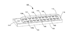
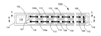
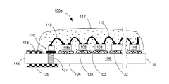
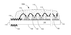
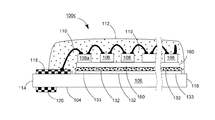
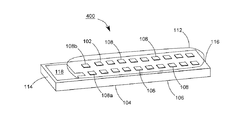
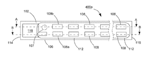
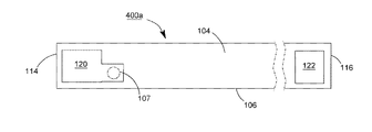
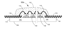
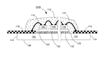
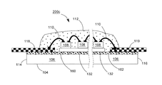
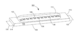
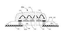
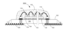
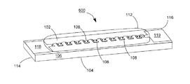
【解決手段】発光ダイオードモジュール100aは、透明基板106と、複数個の発光ダイオードチップ108と、電気線路と、透明カプセルと、2つの電極板118、120とを含む。透明基板106は、それぞれ異なる方向に向く第一表面102と第二表面104とを有する。複数個の発光ダイオードチップ108は、第一表面102上に固定される。電気線路は、複数個の発光ダイオードチップを互いに電気接続させる。透明カプセルは、第一表面102上に設けられ、かつ所定の発光ダイオードチップと電気線路とをほぼ完全に包囲する。2つの電極板118、120は、第一表面102又は第二表面104に接着され、かつ電気線路で所定の発光ダイオードチップ108を電気接続させることにより、発光ダイオードモジュール100aの2つの電源入力端を構成する。
【選択図】図3A
Description
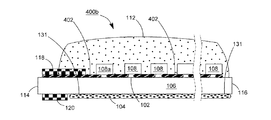
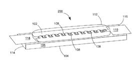
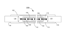
102 上表面
104 下表面
106 透明基板
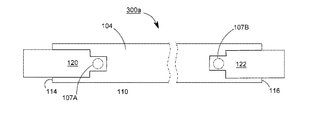
107、107A、107B 導通孔
108、108a、108b 青色光LEDチップ
110 ワイヤ
112 透明接着剤
114、116 端面
118、119、120、122 導電電極板
130 垂直導通部品
131 蛍光層
132、133 透明粘着層
148、150、151、152、154、154a、155、155a、156、157、158 ステップ
160 サブマウント
180 カバー
182 放熱構造
183 電気接続構造
190 はんだ
192 電子回路基板
194 金属固定具
196、198 長状導電部
200、200a、200b、200c、300、300a、300b、400、400a、400b LEDモジュール
402 長状導電部
500a、500 LED電球
502 固定具
600、600a、600b、700 LEDモジュール
Claims (10)
- 異なる方向に向く第一表面と第二表面とを有する透明基板と、
該第一表面上に固定された複数個の発光ダイオードチップと、
該複数個の発光ダイオードチップを互いに電気接続させる電気線路と、
前記第一表面上に設けられるとともに蛍光粉末を含み、該複数個の発光ダイオードチップと前記電気線路とをほぼ完全に包囲する透明カプセルと、
前記第一表面又は前記第二表面に接着され、かつ前記電気線路によって前記所定の発光ダイオードチップに電気接続されることにより、発光ダイオードモジュールの2つの電源入力端を構成する2つの電極板と、
を含むことを特徴とする発光ダイオードモジュール。 - 前記透明カプセルは、蛍光粉末が混合されている透明粘着層を含み、かつ前記いずれかの1個の発光ダイオードチップと前記透明基板との間に設けられることをを特徴とすることをを特徴とする請求項1に記載の発光ダイオードモジュール。
- 前記透明カプセルは複数個の透明粘着層を含み、前記複数個の発光ダイオードチップは一対一の関係に各透明粘着層上に設けられることをを特徴とする請求項1に記載の発光ダイオードモジュール。
- 前記透明カプセルは1個のの透明粘着層を含み、前記複数個の発光ダイオードチップはすべてが該透明粘着層上に設けられることをを特徴とする請求項1に記載の発光ダイオードモジュール。
- 前記透明カプセルは透明接着剤を含み、該透明接着剤は前記複数個の発光ダイオードチップの上部と周辺とを覆うとともに、蛍光粉末を含有することをを特徴とする請求項1に記載の発光ダイオードモジュール。
- 前記複数個の発光ダイオードチップと前記透明粘着層との間に設けられたサブマウントを更に含むことをを特徴とする請求項2に記載の発光ダイオードモジュール。
- 前記複数個の発光ダイオードチップは、フリップチップ方法により前記サブマウント上に固定接着されることをを特徴とする請求項6に記載の発光ダイオードモジュール。
- 前記電気線路は、前記複数個の発光ダイオードチップのうち所定の2個を電気接続させる少なくとも1個のワイヤを含むことをを特徴とする請求項1に記載の発光ダイオードモジュール。
- 前記透明基板は第一端面と第二端面とを含む略長方形体であり、前記2つの電極板はそれぞれ該第一端面の第一表面と第二表面に設けられることをを特徴とする請求項1に記載の発光ダイオードモジュール。
- 前記透明基板は第一端面と第二端面とを含む略長方形体であり、前記2つの電極板はそれぞれ第一端面と第二端面に設けられることをを特徴とする請求項1に記載の発光ダイオードモジュール。
Applications Claiming Priority (4)
| Application Number | Priority Date | Filing Date | Title |
|---|---|---|---|
| TW102122873 | 2013-06-27 | ||
| TW102122873 | 2013-06-27 | ||
| TW103111887 | 2014-03-27 | ||
| TW103111887A TWI651871B (zh) | 2013-06-27 | 2014-03-27 | 發光組件及製作方法 |
Publications (2)
| Publication Number | Publication Date |
|---|---|
| JP2015012292A true JP2015012292A (ja) | 2015-01-19 |
| JP2015012292A5 JP2015012292A5 (ja) | 2017-08-03 |
Family
ID=52115413
Family Applications (1)
| Application Number | Title | Priority Date | Filing Date |
|---|---|---|---|
| JP2014129754A Pending JP2015012292A (ja) | 2013-06-27 | 2014-06-25 | 発光モジュール及びその製造方法 |
Country Status (4)
| Country | Link |
|---|---|
| US (3) | US20150003038A1 (ja) |
| JP (1) | JP2015012292A (ja) |
| CN (2) | CN104253200B (ja) |
| TW (1) | TWI651871B (ja) |
Cited By (3)
| Publication number | Priority date | Publication date | Assignee | Title |
|---|---|---|---|---|
| JP2017028205A (ja) * | 2015-07-27 | 2017-02-02 | ウシオ電機株式会社 | 光源装置 |
| JP2017103232A (ja) * | 2015-12-02 | 2017-06-08 | 羅冠傑 | シェル一体型発光ダイオードアセンブリ、シェル一体型発光ダイオードランプ、およびそれらの製造方法 |
| JP2022544879A (ja) * | 2019-11-07 | 2022-10-21 | シグニファイ ホールディング ビー ヴィ | 3つのタイプのledを備える発光ダイオードフィラメント |
Families Citing this family (20)
| Publication number | Priority date | Publication date | Assignee | Title |
|---|---|---|---|---|
| TW201543720A (zh) * | 2014-05-06 | 2015-11-16 | Genesis Photonics Inc | 封裝結構及其製備方法 |
| US12007077B2 (en) | 2014-09-28 | 2024-06-11 | Zhejiang Super Lighting Electric Appliance Co., Ltd. | LED filament and LED light bulb |
| US11085591B2 (en) | 2014-09-28 | 2021-08-10 | Zhejiang Super Lighting Electric Appliance Co., Ltd | LED light bulb with curved filament |
| US11686436B2 (en) | 2014-09-28 | 2023-06-27 | Zhejiang Super Lighting Electric Appliance Co., Ltd | LED filament and light bulb using LED filament |
| US20220078892A1 (en) * | 2014-09-28 | 2022-03-10 | Zhejiang Super Lighting Electric Appliance Co.,Ltd | Led filament and led light bulb |
| US11073248B2 (en) | 2014-09-28 | 2021-07-27 | Zhejiang Super Lighting Electric Appliance Co., Ltd. | LED bulb lamp |
| US11997768B2 (en) | 2014-09-28 | 2024-05-28 | Zhejiang Super Lighting Electric Appliance Co., Ltd | LED filament and LED light bulb |
| CN106369367A (zh) * | 2015-07-23 | 2017-02-01 | 晶元光电股份有限公司 | 发光装置 |
| DE102015112536A1 (de) * | 2015-07-30 | 2017-02-02 | Osram Opto Semiconductors Gmbh | Optoelektronisches Steckmodul und Beleuchtungsanordnung für den Innenraum einer Fahrzeugkabine |
| DE102015120085A1 (de) * | 2015-11-19 | 2017-05-24 | Osram Opto Semiconductors Gmbh | LED-Filamente, Verfahren zur Herstellung von LED-Filamenten und Retrofitlampe mit LED-Filament |
| CN106449618A (zh) * | 2016-01-29 | 2017-02-22 | 罗冠杰 | 灯壳整合型发光二极管装置及其制作方法 |
| JP2017181815A (ja) * | 2016-03-30 | 2017-10-05 | パナソニック液晶ディスプレイ株式会社 | 液晶表示装置 |
| KR101995000B1 (ko) * | 2016-05-16 | 2019-07-01 | 엘지이노텍 주식회사 | 발광소자 패키지 및 조명장치 |
| CN106151905A (zh) * | 2016-08-15 | 2016-11-23 | 浙江阳光美加照明有限公司 | 一种led发光灯丝及使用该led发光灯丝的led球泡灯 |
| KR102400151B1 (ko) | 2017-05-31 | 2022-05-20 | 서울반도체 주식회사 | 엘이디 패키지 세트 및 이를 포함하는 엘이디 벌브 |
| EP3422826A1 (en) * | 2017-06-26 | 2019-01-02 | Koninklijke Philips N.V. | An apparatus and a method of manufacturing an apparatus |
| US10982048B2 (en) | 2018-04-17 | 2021-04-20 | Jiaxing Super Lighting Electric Appliance Co., Ltd | Organosilicon-modified polyimide resin composition and use thereof |
| PL3963252T3 (pl) * | 2019-05-02 | 2024-03-25 | Signify Holding B.V. | Lampa z włóknami z diodami led |
| TWI712188B (zh) | 2019-11-13 | 2020-12-01 | 隆達電子股份有限公司 | 發光封裝結構及其製造方法 |
| JP7508782B2 (ja) * | 2020-01-20 | 2024-07-02 | 株式会社リコー | 電子デバイス及びその製造方法、画像形成方法、並びに画像形成装置 |
Citations (13)
| Publication number | Priority date | Publication date | Assignee | Title |
|---|---|---|---|---|
| JP2000347601A (ja) * | 1999-06-02 | 2000-12-15 | Toshiba Electronic Engineering Corp | 発光装置 |
| JP2004207649A (ja) * | 2002-12-26 | 2004-07-22 | Rohm Co Ltd | 発光装置及び照明装置 |
| JP2007165811A (ja) * | 2005-12-16 | 2007-06-28 | Nichia Chem Ind Ltd | 発光装置 |
| JP2008251664A (ja) * | 2007-03-29 | 2008-10-16 | Toshiba Lighting & Technology Corp | 照明装置 |
| JP2009004698A (ja) * | 2007-06-25 | 2009-01-08 | Kyocera Corp | 照明用光源 |
| JP2010073592A (ja) * | 2008-09-22 | 2010-04-02 | Toshiba Lighting & Technology Corp | 照明装置 |
| JP2011233801A (ja) * | 2010-04-30 | 2011-11-17 | Rohm Co Ltd | 発光素子モジュール |
| WO2012053134A1 (ja) * | 2010-10-22 | 2012-04-26 | パナソニック株式会社 | 実装用基板、発光装置及びランプ |
| WO2012086109A1 (ja) * | 2010-12-24 | 2012-06-28 | パナソニック株式会社 | 電球形ランプ及び照明装置 |
| WO2012095931A1 (ja) * | 2011-01-14 | 2012-07-19 | パナソニック株式会社 | ランプ及び照明装置 |
| JP2012146738A (ja) * | 2011-01-07 | 2012-08-02 | Stanley Electric Co Ltd | Ledモジュール及びledランプ |
| US20120248469A1 (en) * | 2011-03-30 | 2012-10-04 | Seoul Semiconductor Co., Ltd. | Light emitting apparatus |
| JP2013522850A (ja) * | 2010-09-08 | 2013-06-13 | 浙江鋭迪生光電有限公司 | LED電球及び4π出光可能なLED発光ストリップ |
Family Cites Families (29)
| Publication number | Priority date | Publication date | Assignee | Title |
|---|---|---|---|---|
| US5924784A (en) * | 1995-08-21 | 1999-07-20 | Chliwnyj; Alex | Microprocessor based simulated electronic flame |
| US6147411A (en) * | 1998-03-31 | 2000-11-14 | Micron Technology, Inc. | Vertical surface mount package utilizing a back-to-back semiconductor device module |
| JP3400958B2 (ja) | 1999-07-07 | 2003-04-28 | 株式会社シチズン電子 | 多色発光ダイオード |
| JP4709405B2 (ja) | 2001-03-15 | 2011-06-22 | シチズン電子株式会社 | 発光ダイオード |
| CN1759492B (zh) * | 2003-03-10 | 2010-04-28 | 丰田合成株式会社 | 固体元件装置的制造方法 |
| JP4905009B2 (ja) | 2006-09-12 | 2012-03-28 | 豊田合成株式会社 | 発光装置の製造方法 |
| KR101361575B1 (ko) * | 2007-09-17 | 2014-02-13 | 삼성전자주식회사 | 발광 다이오드 패키지 및 그 제조방법 |
| JP2009259544A (ja) * | 2008-04-15 | 2009-11-05 | Fujitsu Ltd | コネクタ |
| CN101562139B (zh) * | 2008-04-15 | 2011-09-28 | 宏齐科技股份有限公司 | 避免降低发光效率的发光芯片封装结构及其制作方法 |
| JP2009267289A (ja) | 2008-04-30 | 2009-11-12 | Citizen Electronics Co Ltd | 発光装置 |
| CN101800270A (zh) * | 2009-02-11 | 2010-08-11 | 亿光电子工业股份有限公司 | 发光二极管装置及其封装方法 |
| JP2011071242A (ja) * | 2009-09-24 | 2011-04-07 | Toshiba Lighting & Technology Corp | 発光装置及び照明装置 |
| JP5340879B2 (ja) * | 2009-10-13 | 2013-11-13 | スタンレー電気株式会社 | 発光装置 |
| JP5047264B2 (ja) * | 2009-12-22 | 2012-10-10 | 株式会社東芝 | 発光装置 |
| CN202281057U (zh) * | 2011-05-11 | 2012-06-20 | 浙江锐迪生光电有限公司 | 一种LED芯片4π出光的高效率LED发光管 |
| US8371715B2 (en) * | 2010-09-21 | 2013-02-12 | Catcher Technology Co., Ltd. | LED illuminator module with high heat-dissipating efficiency and manufacturing method therefor |
| EP2672175A3 (en) * | 2010-11-04 | 2017-07-19 | Panasonic Intellectual Property Management Co., Ltd. | Light bulb shaped lamp and lighting apparatus |
| JP2012099726A (ja) | 2010-11-04 | 2012-05-24 | Stanley Electric Co Ltd | Ledモジュール及びledランプ |
| US8410726B2 (en) * | 2011-02-22 | 2013-04-02 | Quarkstar Llc | Solid state lamp using modular light emitting elements |
| CN102842667B (zh) * | 2011-06-24 | 2015-02-04 | 展晶科技(深圳)有限公司 | 发光二极管封装结构及其制造方法 |
| CN102956625A (zh) * | 2011-08-18 | 2013-03-06 | 鸿富锦精密工业(深圳)有限公司 | 发光装置 |
| CN103339751B (zh) | 2011-11-15 | 2016-12-14 | 松下知识产权经营株式会社 | 发光模块以及使用该发光模块的灯 |
| CN102496674A (zh) * | 2011-12-23 | 2012-06-13 | 惠州市华阳多媒体电子有限公司 | 一种新型达成白光的led封装结构及封装方法 |
| JP5895166B2 (ja) | 2012-02-13 | 2016-03-30 | パナソニックIpマネジメント株式会社 | 発光モジュール、ランプ及び照明装置 |
| US8928012B2 (en) * | 2012-02-22 | 2015-01-06 | Jianhua Hu | AC LED device and its manufacturing process for general lighting applications |
| TWI499031B (zh) * | 2012-03-22 | 2015-09-01 | Kun Hsin Technology Inc | 發光裝置 |
| WO2014041721A1 (ja) * | 2012-09-11 | 2014-03-20 | パナソニック株式会社 | 照明用光源及び照明装置 |
| JP2014129754A (ja) * | 2012-12-28 | 2014-07-10 | Nissan Motor Co Ltd | 排熱回収装置 |
| TWM455263U (zh) | 2013-01-28 | 2013-06-11 | Harvatek Corp | 複數個藍光發光二極體的白光封裝 |
-
2014
- 2014-03-27 TW TW103111887A patent/TWI651871B/zh active
- 2014-06-19 US US14/309,828 patent/US20150003038A1/en not_active Abandoned
- 2014-06-25 JP JP2014129754A patent/JP2015012292A/ja active Pending
- 2014-06-27 CN CN201410298192.9A patent/CN104253200B/zh active Active
- 2014-06-27 CN CN202010156075.4A patent/CN111457260B/zh active Active
-
2020
- 2020-11-06 US US17/091,938 patent/US11543081B2/en active Active
-
2022
- 2022-12-30 US US18/091,922 patent/US20230142465A1/en not_active Abandoned
Patent Citations (13)
| Publication number | Priority date | Publication date | Assignee | Title |
|---|---|---|---|---|
| JP2000347601A (ja) * | 1999-06-02 | 2000-12-15 | Toshiba Electronic Engineering Corp | 発光装置 |
| JP2004207649A (ja) * | 2002-12-26 | 2004-07-22 | Rohm Co Ltd | 発光装置及び照明装置 |
| JP2007165811A (ja) * | 2005-12-16 | 2007-06-28 | Nichia Chem Ind Ltd | 発光装置 |
| JP2008251664A (ja) * | 2007-03-29 | 2008-10-16 | Toshiba Lighting & Technology Corp | 照明装置 |
| JP2009004698A (ja) * | 2007-06-25 | 2009-01-08 | Kyocera Corp | 照明用光源 |
| JP2010073592A (ja) * | 2008-09-22 | 2010-04-02 | Toshiba Lighting & Technology Corp | 照明装置 |
| JP2011233801A (ja) * | 2010-04-30 | 2011-11-17 | Rohm Co Ltd | 発光素子モジュール |
| JP2013522850A (ja) * | 2010-09-08 | 2013-06-13 | 浙江鋭迪生光電有限公司 | LED電球及び4π出光可能なLED発光ストリップ |
| WO2012053134A1 (ja) * | 2010-10-22 | 2012-04-26 | パナソニック株式会社 | 実装用基板、発光装置及びランプ |
| WO2012086109A1 (ja) * | 2010-12-24 | 2012-06-28 | パナソニック株式会社 | 電球形ランプ及び照明装置 |
| JP2012146738A (ja) * | 2011-01-07 | 2012-08-02 | Stanley Electric Co Ltd | Ledモジュール及びledランプ |
| WO2012095931A1 (ja) * | 2011-01-14 | 2012-07-19 | パナソニック株式会社 | ランプ及び照明装置 |
| US20120248469A1 (en) * | 2011-03-30 | 2012-10-04 | Seoul Semiconductor Co., Ltd. | Light emitting apparatus |
Cited By (3)
| Publication number | Priority date | Publication date | Assignee | Title |
|---|---|---|---|---|
| JP2017028205A (ja) * | 2015-07-27 | 2017-02-02 | ウシオ電機株式会社 | 光源装置 |
| JP2017103232A (ja) * | 2015-12-02 | 2017-06-08 | 羅冠傑 | シェル一体型発光ダイオードアセンブリ、シェル一体型発光ダイオードランプ、およびそれらの製造方法 |
| JP2022544879A (ja) * | 2019-11-07 | 2022-10-21 | シグニファイ ホールディング ビー ヴィ | 3つのタイプのledを備える発光ダイオードフィラメント |
Also Published As
| Publication number | Publication date |
|---|---|
| US20150003038A1 (en) | 2015-01-01 |
| US20210054972A1 (en) | 2021-02-25 |
| CN111457260A (zh) | 2020-07-28 |
| CN104253200B (zh) | 2020-04-07 |
| CN111457260B (zh) | 2022-06-07 |
| TW201501364A (zh) | 2015-01-01 |
| CN104253200A (zh) | 2014-12-31 |
| US11543081B2 (en) | 2023-01-03 |
| US20230142465A1 (en) | 2023-05-11 |
| TWI651871B (zh) | 2019-02-21 |
Similar Documents
| Publication | Publication Date | Title |
|---|---|---|
| JP6949089B2 (ja) | 発光モジュール及びその製造方法 | |
| JP2015012292A (ja) | 発光モジュール及びその製造方法 | |
| JP7015278B2 (ja) | 発光ダイオードモジュール及びその製造方法 | |
| JP6616065B2 (ja) | 発光モジュール及びそれに関する照明装置 | |
| JP4935514B2 (ja) | 発光装置 | |
| US9966509B2 (en) | Light emitting apparatus and lighting apparatus | |
| KR20140118466A (ko) | 발광 디바이스 및 이를 포함하는 조명장치 | |
| TWI613842B (zh) | 發光裝置 | |
| TWI390703B (zh) | 正向發光之發光二極體封裝結構及製程 | |
| JP2011507285A (ja) | オプトエレクトロニクス素子 | |
| US10088133B2 (en) | Mounting substrate, light-emitting apparatus, and illumination apparatus | |
| JP2016072263A (ja) | 発光モジュールおよび照明装置 | |
| TWI407546B (zh) | 側向發光之半導體元件封裝結構 | |
| JP3186004U (ja) | チップ未封止led照明 | |
| US20120273809A1 (en) | Light emitting diode device | |
| TWI711188B (zh) | 發光二極體組件 | |
| TWI774091B (zh) | 發光二極體組件 | |
| TWI676300B (zh) | 發光二極體組件 | |
| CN104282817A (zh) | 发光二极管组件及制作方法 | |
| TWI713236B (zh) | 發光二極體組件及製作方法 | |
| KR20120082191A (ko) | 발광소자 패키지 |
Legal Events
| Date | Code | Title | Description |
|---|---|---|---|
| A521 | Request for written amendment filed |
Free format text: JAPANESE INTERMEDIATE CODE: A523 Effective date: 20170622 |
|
| A621 | Written request for application examination |
Free format text: JAPANESE INTERMEDIATE CODE: A621 Effective date: 20170622 |
|
| A977 | Report on retrieval |
Free format text: JAPANESE INTERMEDIATE CODE: A971007 Effective date: 20180214 |
|
| A131 | Notification of reasons for refusal |
Free format text: JAPANESE INTERMEDIATE CODE: A131 Effective date: 20180320 |
|
| A711 | Notification of change in applicant |
Free format text: JAPANESE INTERMEDIATE CODE: A711 Effective date: 20180530 Free format text: JAPANESE INTERMEDIATE CODE: A712 Effective date: 20180530 |
|
| A521 | Request for written amendment filed |
Free format text: JAPANESE INTERMEDIATE CODE: A523 Effective date: 20180615 |
|
| A521 | Request for written amendment filed |
Free format text: JAPANESE INTERMEDIATE CODE: A523 Effective date: 20180730 |
|
| A521 | Request for written amendment filed |
Free format text: JAPANESE INTERMEDIATE CODE: A523 Effective date: 20180821 |
|
| A02 | Decision of refusal |
Free format text: JAPANESE INTERMEDIATE CODE: A02 Effective date: 20180904 |
|
| A521 | Request for written amendment filed |
Free format text: JAPANESE INTERMEDIATE CODE: A523 Effective date: 20181228 |
|
| A911 | Transfer to examiner for re-examination before appeal (zenchi) |
Free format text: JAPANESE INTERMEDIATE CODE: A911 Effective date: 20190109 |
|
| A912 | Re-examination (zenchi) completed and case transferred to appeal board |
Free format text: JAPANESE INTERMEDIATE CODE: A912 Effective date: 20190208 |
|
| A521 | Request for written amendment filed |
Free format text: JAPANESE INTERMEDIATE CODE: A523 Effective date: 20200323 |
