JP2014165252A - Film formation method, program, computer storage medium, and film formation system - Google Patents
Film formation method, program, computer storage medium, and film formation system Download PDFInfo
- Publication number
- JP2014165252A JP2014165252A JP2013033216A JP2013033216A JP2014165252A JP 2014165252 A JP2014165252 A JP 2014165252A JP 2013033216 A JP2013033216 A JP 2013033216A JP 2013033216 A JP2013033216 A JP 2013033216A JP 2014165252 A JP2014165252 A JP 2014165252A
- Authority
- JP
- Japan
- Prior art keywords
- film
- heat treatment
- ultraviolet irradiation
- organic film
- wafer
- Prior art date
- Legal status (The legal status is an assumption and is not a legal conclusion. Google has not performed a legal analysis and makes no representation as to the accuracy of the status listed.)
- Granted
Links
- 230000015572 biosynthetic process Effects 0.000 title claims abstract description 7
- 238000000034 method Methods 0.000 title claims description 70
- 238000003860 storage Methods 0.000 title claims description 6
- 238000010438 heat treatment Methods 0.000 claims abstract description 137
- 239000011368 organic material Substances 0.000 claims abstract description 55
- 238000000576 coating method Methods 0.000 claims abstract description 40
- 239000011248 coating agent Substances 0.000 claims abstract description 34
- 239000000758 substrate Substances 0.000 claims abstract description 29
- 238000012545 processing Methods 0.000 claims description 135
- QVGXLLKOCUKJST-UHFFFAOYSA-N atomic oxygen Chemical compound [O] QVGXLLKOCUKJST-UHFFFAOYSA-N 0.000 claims description 15
- 229910052760 oxygen Inorganic materials 0.000 claims description 15
- 239000001301 oxygen Substances 0.000 claims description 15
- 238000005259 measurement Methods 0.000 claims description 13
- 239000011810 insulating material Substances 0.000 claims description 11
- 235000012431 wafers Nutrition 0.000 description 179
- 238000012546 transfer Methods 0.000 description 23
- 239000007789 gas Substances 0.000 description 18
- 230000003028 elevating effect Effects 0.000 description 11
- CBENFWSGALASAD-UHFFFAOYSA-N Ozone Chemical compound [O-][O+]=O CBENFWSGALASAD-UHFFFAOYSA-N 0.000 description 7
- 238000001312 dry etching Methods 0.000 description 6
- 239000007788 liquid Substances 0.000 description 6
- 230000001590 oxidative effect Effects 0.000 description 6
- 238000004519 manufacturing process Methods 0.000 description 5
- 238000001514 detection method Methods 0.000 description 4
- 230000001678 irradiating effect Effects 0.000 description 4
- 238000009826 distribution Methods 0.000 description 3
- 230000000694 effects Effects 0.000 description 3
- 239000011521 glass Substances 0.000 description 3
- 239000010410 layer Substances 0.000 description 3
- 230000003287 optical effect Effects 0.000 description 3
- 239000004065 semiconductor Substances 0.000 description 3
- 239000000126 substance Substances 0.000 description 3
- 229910004298 SiO 2 Inorganic materials 0.000 description 2
- 238000004140 cleaning Methods 0.000 description 2
- 238000005530 etching Methods 0.000 description 2
- 239000011229 interlayer Substances 0.000 description 2
- 239000000463 material Substances 0.000 description 2
- 238000012986 modification Methods 0.000 description 2
- 230000004048 modification Effects 0.000 description 2
- 239000012044 organic layer Substances 0.000 description 2
- VYPSYNLAJGMNEJ-UHFFFAOYSA-N Silicium dioxide Chemical compound O=[Si]=O VYPSYNLAJGMNEJ-UHFFFAOYSA-N 0.000 description 1
- 230000007423 decrease Effects 0.000 description 1
- 230000003247 decreasing effect Effects 0.000 description 1
- 230000000994 depressogenic effect Effects 0.000 description 1
- 238000011161 development Methods 0.000 description 1
- 238000007599 discharging Methods 0.000 description 1
- 229910052736 halogen Inorganic materials 0.000 description 1
- 150000002367 halogens Chemical class 0.000 description 1
- 239000000203 mixture Substances 0.000 description 1
- 230000002093 peripheral effect Effects 0.000 description 1
- 238000001020 plasma etching Methods 0.000 description 1
- 230000036632 reaction speed Effects 0.000 description 1
- 239000002904 solvent Substances 0.000 description 1
- 239000007921 spray Substances 0.000 description 1
Images


Classifications
-
- H—ELECTRICITY
- H01—ELECTRIC ELEMENTS
- H01L—SEMICONDUCTOR DEVICES NOT COVERED BY CLASS H10
- H01L21/00—Processes or apparatus adapted for the manufacture or treatment of semiconductor or solid state devices or of parts thereof
- H01L21/02—Manufacture or treatment of semiconductor devices or of parts thereof
- H01L21/02104—Forming layers
- H01L21/02107—Forming insulating materials on a substrate
- H01L21/02296—Forming insulating materials on a substrate characterised by the treatment performed before or after the formation of the layer
- H01L21/02318—Forming insulating materials on a substrate characterised by the treatment performed before or after the formation of the layer post-treatment
- H01L21/02345—Forming insulating materials on a substrate characterised by the treatment performed before or after the formation of the layer post-treatment treatment by exposure to radiation, e.g. visible light
- H01L21/02348—Forming insulating materials on a substrate characterised by the treatment performed before or after the formation of the layer post-treatment treatment by exposure to radiation, e.g. visible light treatment by exposure to UV light
-
- H—ELECTRICITY
- H01—ELECTRIC ELEMENTS
- H01L—SEMICONDUCTOR DEVICES NOT COVERED BY CLASS H10
- H01L21/00—Processes or apparatus adapted for the manufacture or treatment of semiconductor or solid state devices or of parts thereof
- H01L21/02—Manufacture or treatment of semiconductor devices or of parts thereof
- H01L21/04—Manufacture or treatment of semiconductor devices or of parts thereof the devices having potential barriers, e.g. a PN junction, depletion layer or carrier concentration layer
- H01L21/18—Manufacture or treatment of semiconductor devices or of parts thereof the devices having potential barriers, e.g. a PN junction, depletion layer or carrier concentration layer the devices having semiconductor bodies comprising elements of Group IV of the Periodic Table or AIIIBV compounds with or without impurities, e.g. doping materials
- H01L21/30—Treatment of semiconductor bodies using processes or apparatus not provided for in groups H01L21/20 - H01L21/26
- H01L21/31—Treatment of semiconductor bodies using processes or apparatus not provided for in groups H01L21/20 - H01L21/26 to form insulating layers thereon, e.g. for masking or by using photolithographic techniques; After treatment of these layers; Selection of materials for these layers
- H01L21/3105—After-treatment
- H01L21/31051—Planarisation of the insulating layers
- H01L21/31053—Planarisation of the insulating layers involving a dielectric removal step
- H01L21/31055—Planarisation of the insulating layers involving a dielectric removal step the removal being a chemical etching step, e.g. dry etching
-
- B—PERFORMING OPERATIONS; TRANSPORTING
- B05—SPRAYING OR ATOMISING IN GENERAL; APPLYING FLUENT MATERIALS TO SURFACES, IN GENERAL
- B05C—APPARATUS FOR APPLYING FLUENT MATERIALS TO SURFACES, IN GENERAL
- B05C11/00—Component parts, details or accessories not specifically provided for in groups B05C1/00 - B05C9/00
- B05C11/10—Storage, supply or control of liquid or other fluent material; Recovery of excess liquid or other fluent material
- B05C11/1002—Means for controlling supply, i.e. flow or pressure, of liquid or other fluent material to the applying apparatus, e.g. valves
- B05C11/1015—Means for controlling supply, i.e. flow or pressure, of liquid or other fluent material to the applying apparatus, e.g. valves responsive to a conditions of ambient medium or target, e.g. humidity, temperature ; responsive to position or movement of the coating head relative to the target
-
- B—PERFORMING OPERATIONS; TRANSPORTING
- B05—SPRAYING OR ATOMISING IN GENERAL; APPLYING FLUENT MATERIALS TO SURFACES, IN GENERAL
- B05C—APPARATUS FOR APPLYING FLUENT MATERIALS TO SURFACES, IN GENERAL
- B05C9/00—Apparatus or plant for applying liquid or other fluent material to surfaces by means not covered by any preceding group, or in which the means of applying the liquid or other fluent material is not important
- B05C9/08—Apparatus or plant for applying liquid or other fluent material to surfaces by means not covered by any preceding group, or in which the means of applying the liquid or other fluent material is not important for applying liquid or other fluent material and performing an auxiliary operation
- B05C9/12—Apparatus or plant for applying liquid or other fluent material to surfaces by means not covered by any preceding group, or in which the means of applying the liquid or other fluent material is not important for applying liquid or other fluent material and performing an auxiliary operation the auxiliary operation being performed after the application
-
- B—PERFORMING OPERATIONS; TRANSPORTING
- B05—SPRAYING OR ATOMISING IN GENERAL; APPLYING FLUENT MATERIALS TO SURFACES, IN GENERAL
- B05C—APPARATUS FOR APPLYING FLUENT MATERIALS TO SURFACES, IN GENERAL
- B05C9/00—Apparatus or plant for applying liquid or other fluent material to surfaces by means not covered by any preceding group, or in which the means of applying the liquid or other fluent material is not important
- B05C9/08—Apparatus or plant for applying liquid or other fluent material to surfaces by means not covered by any preceding group, or in which the means of applying the liquid or other fluent material is not important for applying liquid or other fluent material and performing an auxiliary operation
- B05C9/14—Apparatus or plant for applying liquid or other fluent material to surfaces by means not covered by any preceding group, or in which the means of applying the liquid or other fluent material is not important for applying liquid or other fluent material and performing an auxiliary operation the auxiliary operation involving heating or cooling
-
- H—ELECTRICITY
- H01—ELECTRIC ELEMENTS
- H01L—SEMICONDUCTOR DEVICES NOT COVERED BY CLASS H10
- H01L21/00—Processes or apparatus adapted for the manufacture or treatment of semiconductor or solid state devices or of parts thereof
- H01L21/02—Manufacture or treatment of semiconductor devices or of parts thereof
- H01L21/027—Making masks on semiconductor bodies for further photolithographic processing not provided for in group H01L21/18 or H01L21/34
- H01L21/0271—Making masks on semiconductor bodies for further photolithographic processing not provided for in group H01L21/18 or H01L21/34 comprising organic layers
-
- H—ELECTRICITY
- H01—ELECTRIC ELEMENTS
- H01L—SEMICONDUCTOR DEVICES NOT COVERED BY CLASS H10
- H01L21/00—Processes or apparatus adapted for the manufacture or treatment of semiconductor or solid state devices or of parts thereof
- H01L21/02—Manufacture or treatment of semiconductor devices or of parts thereof
- H01L21/04—Manufacture or treatment of semiconductor devices or of parts thereof the devices having potential barriers, e.g. a PN junction, depletion layer or carrier concentration layer
- H01L21/18—Manufacture or treatment of semiconductor devices or of parts thereof the devices having potential barriers, e.g. a PN junction, depletion layer or carrier concentration layer the devices having semiconductor bodies comprising elements of Group IV of the Periodic Table or AIIIBV compounds with or without impurities, e.g. doping materials
- H01L21/30—Treatment of semiconductor bodies using processes or apparatus not provided for in groups H01L21/20 - H01L21/26
- H01L21/31—Treatment of semiconductor bodies using processes or apparatus not provided for in groups H01L21/20 - H01L21/26 to form insulating layers thereon, e.g. for masking or by using photolithographic techniques; After treatment of these layers; Selection of materials for these layers
- H01L21/3105—After-treatment
- H01L21/311—Etching the insulating layers by chemical or physical means
- H01L21/31127—Etching organic layers
- H01L21/31133—Etching organic layers by chemical means
- H01L21/31138—Etching organic layers by chemical means by dry-etching
-
- H—ELECTRICITY
- H01—ELECTRIC ELEMENTS
- H01L—SEMICONDUCTOR DEVICES NOT COVERED BY CLASS H10
- H01L21/00—Processes or apparatus adapted for the manufacture or treatment of semiconductor or solid state devices or of parts thereof
- H01L21/67—Apparatus specially adapted for handling semiconductor or electric solid state devices during manufacture or treatment thereof; Apparatus specially adapted for handling wafers during manufacture or treatment of semiconductor or electric solid state devices or components ; Apparatus not specifically provided for elsewhere
- H01L21/67005—Apparatus not specifically provided for elsewhere
- H01L21/67011—Apparatus for manufacture or treatment
- H01L21/67098—Apparatus for thermal treatment
- H01L21/67109—Apparatus for thermal treatment mainly by convection
-
- H—ELECTRICITY
- H01—ELECTRIC ELEMENTS
- H01L—SEMICONDUCTOR DEVICES NOT COVERED BY CLASS H10
- H01L21/00—Processes or apparatus adapted for the manufacture or treatment of semiconductor or solid state devices or of parts thereof
- H01L21/67—Apparatus specially adapted for handling semiconductor or electric solid state devices during manufacture or treatment thereof; Apparatus specially adapted for handling wafers during manufacture or treatment of semiconductor or electric solid state devices or components ; Apparatus not specifically provided for elsewhere
- H01L21/67005—Apparatus not specifically provided for elsewhere
- H01L21/67011—Apparatus for manufacture or treatment
- H01L21/67098—Apparatus for thermal treatment
- H01L21/67115—Apparatus for thermal treatment mainly by radiation
-
- H—ELECTRICITY
- H01—ELECTRIC ELEMENTS
- H01L—SEMICONDUCTOR DEVICES NOT COVERED BY CLASS H10
- H01L21/00—Processes or apparatus adapted for the manufacture or treatment of semiconductor or solid state devices or of parts thereof
- H01L21/67—Apparatus specially adapted for handling semiconductor or electric solid state devices during manufacture or treatment thereof; Apparatus specially adapted for handling wafers during manufacture or treatment of semiconductor or electric solid state devices or components ; Apparatus not specifically provided for elsewhere
- H01L21/67005—Apparatus not specifically provided for elsewhere
- H01L21/67011—Apparatus for manufacture or treatment
- H01L21/6715—Apparatus for applying a liquid, a resin, an ink or the like
-
- H—ELECTRICITY
- H01—ELECTRIC ELEMENTS
- H01L—SEMICONDUCTOR DEVICES NOT COVERED BY CLASS H10
- H01L21/00—Processes or apparatus adapted for the manufacture or treatment of semiconductor or solid state devices or of parts thereof
- H01L21/67—Apparatus specially adapted for handling semiconductor or electric solid state devices during manufacture or treatment thereof; Apparatus specially adapted for handling wafers during manufacture or treatment of semiconductor or electric solid state devices or components ; Apparatus not specifically provided for elsewhere
- H01L21/67005—Apparatus not specifically provided for elsewhere
- H01L21/67011—Apparatus for manufacture or treatment
- H01L21/67155—Apparatus for manufacturing or treating in a plurality of work-stations
- H01L21/67161—Apparatus for manufacturing or treating in a plurality of work-stations characterized by the layout of the process chambers
- H01L21/67178—Apparatus for manufacturing or treating in a plurality of work-stations characterized by the layout of the process chambers vertical arrangement
-
- H—ELECTRICITY
- H01—ELECTRIC ELEMENTS
- H01L—SEMICONDUCTOR DEVICES NOT COVERED BY CLASS H10
- H01L21/00—Processes or apparatus adapted for the manufacture or treatment of semiconductor or solid state devices or of parts thereof
- H01L21/67—Apparatus specially adapted for handling semiconductor or electric solid state devices during manufacture or treatment thereof; Apparatus specially adapted for handling wafers during manufacture or treatment of semiconductor or electric solid state devices or components ; Apparatus not specifically provided for elsewhere
- H01L21/67005—Apparatus not specifically provided for elsewhere
- H01L21/67011—Apparatus for manufacture or treatment
- H01L21/67155—Apparatus for manufacturing or treating in a plurality of work-stations
- H01L21/6719—Apparatus for manufacturing or treating in a plurality of work-stations characterized by the construction of the processing chambers, e.g. modular processing chambers
-
- H—ELECTRICITY
- H01—ELECTRIC ELEMENTS
- H01L—SEMICONDUCTOR DEVICES NOT COVERED BY CLASS H10
- H01L22/00—Testing or measuring during manufacture or treatment; Reliability measurements, i.e. testing of parts without further processing to modify the parts as such; Structural arrangements therefor
- H01L22/20—Sequence of activities consisting of a plurality of measurements, corrections, marking or sorting steps
- H01L22/26—Acting in response to an ongoing measurement without interruption of processing, e.g. endpoint detection, in-situ thickness measurement
-
- B—PERFORMING OPERATIONS; TRANSPORTING
- B05—SPRAYING OR ATOMISING IN GENERAL; APPLYING FLUENT MATERIALS TO SURFACES, IN GENERAL
- B05C—APPARATUS FOR APPLYING FLUENT MATERIALS TO SURFACES, IN GENERAL
- B05C11/00—Component parts, details or accessories not specifically provided for in groups B05C1/00 - B05C9/00
- B05C11/02—Apparatus for spreading or distributing liquids or other fluent materials already applied to a surface ; Controlling means therefor; Control of the thickness of a coating by spreading or distributing liquids or other fluent materials already applied to the coated surface
- B05C11/08—Spreading liquid or other fluent material by manipulating the work, e.g. tilting
-
- H—ELECTRICITY
- H01—ELECTRIC ELEMENTS
- H01L—SEMICONDUCTOR DEVICES NOT COVERED BY CLASS H10
- H01L21/00—Processes or apparatus adapted for the manufacture or treatment of semiconductor or solid state devices or of parts thereof
- H01L21/02—Manufacture or treatment of semiconductor devices or of parts thereof
- H01L21/02104—Forming layers
- H01L21/02107—Forming insulating materials on a substrate
- H01L21/02109—Forming insulating materials on a substrate characterised by the type of layer, e.g. type of material, porous/non-porous, pre-cursors, mixtures or laminates
- H01L21/02112—Forming insulating materials on a substrate characterised by the type of layer, e.g. type of material, porous/non-porous, pre-cursors, mixtures or laminates characterised by the material of the layer
- H01L21/02118—Forming insulating materials on a substrate characterised by the type of layer, e.g. type of material, porous/non-porous, pre-cursors, mixtures or laminates characterised by the material of the layer carbon based polymeric organic or inorganic material, e.g. polyimides, poly cyclobutene or PVC
-
- H—ELECTRICITY
- H01—ELECTRIC ELEMENTS
- H01L—SEMICONDUCTOR DEVICES NOT COVERED BY CLASS H10
- H01L22/00—Testing or measuring during manufacture or treatment; Reliability measurements, i.e. testing of parts without further processing to modify the parts as such; Structural arrangements therefor
- H01L22/10—Measuring as part of the manufacturing process
- H01L22/12—Measuring as part of the manufacturing process for structural parameters, e.g. thickness, line width, refractive index, temperature, warp, bond strength, defects, optical inspection, electrical measurement of structural dimensions, metallurgic measurement of diffusions
Landscapes
- Engineering & Computer Science (AREA)
- Manufacturing & Machinery (AREA)
- Computer Hardware Design (AREA)
- Microelectronics & Electronic Packaging (AREA)
- Power Engineering (AREA)
- Physics & Mathematics (AREA)
- Condensed Matter Physics & Semiconductors (AREA)
- General Physics & Mathematics (AREA)
- Chemical & Material Sciences (AREA)
- Chemical Kinetics & Catalysis (AREA)
- General Chemical & Material Sciences (AREA)
- Health & Medical Sciences (AREA)
- Toxicology (AREA)
- Formation Of Insulating Films (AREA)
- Exposure Of Semiconductors, Excluding Electron Or Ion Beam Exposure (AREA)
- Internal Circuitry In Semiconductor Integrated Circuit Devices (AREA)
- Cleaning Or Drying Semiconductors (AREA)
- Application Of Or Painting With Fluid Materials (AREA)
Abstract
Description
本発明は、表面にパターンが形成された基板上に有機膜を形成する成膜方法、プログラム、コンピュータ記憶媒体、及び当該成膜方法を実行するための成膜システムに関する。 The present invention relates to a film formation method, a program, a computer storage medium, and a film formation system for executing the film formation method for forming an organic film on a substrate having a pattern formed on the surface.
例えば多層配線構造の半導体デバイスの製造工程では、例えば半導体ウェハ(以下、「ウェハ」という。)上にレジスト液を塗布してレジスト膜を形成するレジスト塗布処理、当該レジスト膜に所定のパターンを露光する露光処理、露光されたレジスト膜を現像する現像処理などが順次行われ、ウェハ上に所定のレジストパターンが形成される。このレジストパターンをマスクとして、ウェハのエッチング処理が行われ、その後レジスト膜の除去処理などが行われて、ウェハ上に所定のパターンが形成される。このように所定の層に所定のパターンが形成される工程が複数回繰り返し行われ、多層配線構造の半導体デバイスが製造される。 For example, in a manufacturing process of a semiconductor device having a multilayer wiring structure, for example, a resist coating process for applying a resist solution on a semiconductor wafer (hereinafter referred to as “wafer”) to form a resist film, and exposing a predetermined pattern on the resist film An exposure process for developing and a development process for developing the exposed resist film are sequentially performed to form a predetermined resist pattern on the wafer. Using this resist pattern as a mask, the wafer is etched, and then the resist film is removed to form a predetermined pattern on the wafer. Thus, the process of forming a predetermined pattern in a predetermined layer is repeated a plurality of times, and a semiconductor device having a multilayer wiring structure is manufactured.
ところで、このようにウェハ上に所定のパターンが繰り返し形成される場合、n層目に所定のパターンが形成された後に、(n+1)層目のレジスト膜が適切な高さに形成されるためには、レジスト液が塗布される面が平坦であることが必要になる。 By the way, when a predetermined pattern is repeatedly formed on the wafer in this way, the (n + 1) -th layer resist film is formed at an appropriate height after the predetermined pattern is formed on the n-th layer. The surface to which the resist solution is applied needs to be flat.
そこで従来より、ウェハの所定のパターン上に有機膜を形成し、その表面を平坦化することが行われている。このような有機膜の形成は、ウェハ上に有機材料を塗布し、塗布された有機材料を加熱して有機膜を形成し、さらに例えばドライエッチング法(反応性イオンエッチング法)によって有機膜をエッチバックして当該有機膜の表面を除去することにより行われる(特許文献1)。また有機膜としては、例えばSOC(Spin On Cap)膜やSOG(Spin On Glass)膜等が用いられる。 Therefore, conventionally, an organic film is formed on a predetermined pattern of a wafer and the surface thereof is flattened. Such an organic film is formed by applying an organic material on the wafer, heating the applied organic material to form the organic film, and further etching the organic film by, for example, dry etching (reactive ion etching). This is performed by backing and removing the surface of the organic film (Patent Document 1). As the organic film, for example, an SOC (Spin On Cap) film or an SOG (Spin On Glass) film is used.
上述した特許文献1に記載された方法を用いた場合、有機材料の塗布と有機材料の加熱はそれぞれ常圧雰囲気下で行われるのに対し、有機膜のエッチバックは真空雰囲気下で行われる。そうすると、これら常圧雰囲気下の処理と真空雰囲気下の処理を別々のシステムで行い、システム間でウェハを搬送する必要がある。このため、システムの製造コストが高額化し、またウェハ処理のスループットも低下する。
When the method described in
また、有機膜のエッチバックをドライエッチング法で行った場合、プラズマによってウェハやウェハ上の膜がプラズマによって損傷を被るおそれがある。さらにこのプラズマによって、ウェハ上の膜が改質されるおそれもある。 Further, when the organic film is etched back by a dry etching method, there is a possibility that the wafer or the film on the wafer may be damaged by the plasma. Further, the plasma may modify the film on the wafer.
本発明は、かかる点に鑑みてなされたものであり、表面にパターンが形成された基板上に有機膜を適切且つ効率よく形成することを目的とする。 This invention is made | formed in view of this point, and it aims at forming an organic film appropriately and efficiently on the board | substrate with which the pattern was formed in the surface.
前記の目的を達成するため、本発明は、表面にパターンが形成された基板上に有機膜を形成する成膜方法であって、基板上に有機材料を塗布する塗布処理工程と、その後、前記有機材料を熱処理して基板上に有機膜を形成する熱処理工程と、その後、前記有機膜に対して紫外線照射処理を行い、当該有機膜の表面を所定の深さまで除去する紫外線照射工程と、を有することを特徴としている。 In order to achieve the above object, the present invention provides a film forming method for forming an organic film on a substrate having a pattern formed on a surface thereof, a coating treatment step for applying an organic material on the substrate, A heat treatment step of heat-treating the organic material to form an organic film on the substrate; and thereafter, an ultraviolet irradiation step of performing an ultraviolet irradiation treatment on the organic film and removing the surface of the organic film to a predetermined depth. It is characterized by having.
本発明によれば、紫外線照射工程において有機膜に対して紫外線照射処理を行う。すなわち、紫外線を照射することによって処理雰囲気中に活性酸素とオゾンが発生し、これら活性酸素とオゾンによって有機膜の表面が分解されて除去される。そして、パターンが形成された領域における表面高さと、パターンの窪み部が形成された領域の表面高さとの差が所定の範囲内になるように、有機膜の表面が除去される。そうすると、表面にパターンが形成された基板上に有機膜が形成される場合であっても、当該有機膜の表面を平坦化することができる。 According to the present invention, the ultraviolet irradiation process is performed on the organic film in the ultraviolet irradiation process. That is, irradiation with ultraviolet rays generates active oxygen and ozone in the processing atmosphere, and the surface of the organic film is decomposed and removed by these active oxygen and ozone. Then, the surface of the organic film is removed so that the difference between the surface height in the region in which the pattern is formed and the surface height in the region in which the pattern depression is formed is within a predetermined range. Then, even when an organic film is formed on a substrate having a pattern formed on the surface, the surface of the organic film can be planarized.
また、紫外線照射処理によって有機膜の表面を除去するので、従来のドライエッチング法を行った場合のように基板や基板上の膜が損傷を被らず、さらに基板上の膜が改質されるおそれもない。したがって、基板上に有機膜を適切に形成することができる。 In addition, since the surface of the organic film is removed by ultraviolet irradiation treatment, the substrate and the film on the substrate are not damaged as in the case of the conventional dry etching method, and the film on the substrate is further modified. There is no fear. Therefore, an organic film can be appropriately formed on the substrate.
しかも本発明によれば、塗布処理工程、熱処理工程及び紫外線照射工程をすべて常圧雰囲気下で行うことができ、これらの工程を一のシステムで行うことができる。したがって、システムの製造コストを低廉化することができ、また基板処理のスループットを向上させることができる。 Moreover, according to the present invention, the coating treatment process, the heat treatment process, and the ultraviolet irradiation process can all be performed under a normal pressure atmosphere, and these processes can be performed with one system. Therefore, the manufacturing cost of the system can be reduced, and the throughput of the substrate processing can be improved.
前記塗布処理工程、前記熱処理工程及び前記紫外線照射工程をそれぞれこの順で複数回行い、少なくとも最後より前に行われる前記紫外線照射工程において、前記パターンの表面が露出するまで、前記有機膜の表面を除去してもよい。 The coating treatment step, the heat treatment step, and the ultraviolet irradiation step are each performed a plurality of times in this order, and in the ultraviolet irradiation step performed at least before the last, the surface of the organic film is exposed until the surface of the pattern is exposed. It may be removed.
前記紫外線照射工程において、前記有機膜を熱処理しながら、前記紫外線照射処理を行ってもよい。 In the ultraviolet irradiation step, the ultraviolet irradiation treatment may be performed while heat-treating the organic film.
前記紫外線照射工程における前記熱処理は、基板を熱処理板に載置して行われてもよい。 The heat treatment in the ultraviolet irradiation step may be performed by placing a substrate on a heat treatment plate.
前記熱処理板は複数設けられ、それぞれ異なる温度で前記紫外線照射工程における前記熱処理が行われてもよい。 A plurality of the heat treatment plates may be provided, and the heat treatment in the ultraviolet irradiation step may be performed at different temperatures.
前記紫外線照射工程における前記熱処理は、光源からの照射光により行われてもよい。 The heat treatment in the ultraviolet irradiation step may be performed by irradiation light from a light source.
前記紫外線照射工程において、少なくとも処理雰囲気の酸素濃度、紫外線の照度又は紫外線の照射時間を制御してもよい。 In the ultraviolet irradiation step, at least the oxygen concentration of the processing atmosphere, the illuminance of ultraviolet rays, or the irradiation time of ultraviolet rays may be controlled.
前記成膜方法は、前記紫外線照射工程後、前記有機膜の膜厚を測定する膜厚測定工程をさらに有し、前記膜厚測定工程における測定結果に基づいて、前記紫外線照射工程の処理条件を補正してもよい。 The film forming method further includes a film thickness measurement step for measuring the film thickness of the organic film after the ultraviolet irradiation step, and based on the measurement result in the film thickness measurement step, the processing conditions of the ultraviolet irradiation step are set. It may be corrected.
別な観点による本発明によれば、前記成膜方法を成膜システムによって実行させるために、当該成膜システムを制御する制御部のコンピュータ上で動作するプログラムが提供される。 According to another aspect of the present invention, there is provided a program that operates on a computer of a control unit that controls the film forming system in order to cause the film forming system to execute the film forming method.
また別な観点による本発明によれば、前記プログラムを格納した読み取り可能なコンピュータ記憶媒体が提供される。 According to another aspect of the present invention, a readable computer storage medium storing the program is provided.
さらに別な観点による本発明は、表面にパターンが形成された基板上に有機膜を形成する成膜システムであって、基板上に有機材料を塗布処理する塗布処理部と、前記有機材料を熱処理して基板上に有機膜を形成する熱処理部と、前記有機膜に対して紫外線照射処理を行う紫外線照射部と、前記塗布処理、前記熱処理及び前記紫外線照射処理をこの順で行い、前記紫外線照射処理において前記有機膜の表面を所定の深さまで除去するように、前記塗布処理部、前記熱処理部及び前記紫外線照射部を制御する制御部と、を有することを特徴としている。 According to yet another aspect, the present invention provides a film forming system for forming an organic film on a substrate having a pattern formed on a surface thereof, a coating processing unit for applying an organic material on the substrate, and heat-treating the organic material. Then, a heat treatment section for forming an organic film on the substrate, an ultraviolet irradiation section for performing ultraviolet irradiation treatment on the organic film, the coating treatment, the heat treatment and the ultraviolet irradiation treatment are performed in this order, and the ultraviolet irradiation is performed. It has a control part which controls the application treatment part, the heat treatment part, and the ultraviolet irradiation part so that the surface of the organic film may be removed to a predetermined depth in the process.
前記制御部は、前記塗布処理、前記熱処理及び前記紫外線照射処理をそれぞれこの順で複数回行い、少なくとも最後より前に行われる前記紫外線照射処理において、前記パターンの表面が露出するまで、前記有機膜の表面を除去するように、前記塗布処理部、前記熱処理部及び前記紫外線照射部を制御してもよい。 The controller performs the coating process, the heat treatment, and the ultraviolet irradiation process a plurality of times in this order, and at least the organic film until the surface of the pattern is exposed in the ultraviolet irradiation process performed before the last. The coating treatment unit, the heat treatment unit, and the ultraviolet irradiation unit may be controlled so as to remove the surface.
前記成膜システムは、前記紫外線照射処理を行う際、当該有機膜を熱処理する他の熱処理部をさらに有していてもよい。 The film forming system may further include another heat treatment unit that heat-treats the organic film when performing the ultraviolet irradiation treatment.
前記他の熱処理部は、基板を載置して熱処理する熱処理板を有していてもよい。 The other heat treatment section may have a heat treatment plate for placing and heat treating the substrate.
前記熱処理板は複数設けられ、それぞれ異なる温度で熱処理を行ってもよい。 A plurality of the heat treatment plates may be provided, and the heat treatment may be performed at different temperatures.
前記他の熱処理部は、前記有機膜に対して照射光を照射する光源を有していてもよい。 The other heat treatment unit may include a light source that irradiates the organic film with irradiation light.
前記熱処理部と前記紫外線照射部は同一装置内に設けられ、当該装置内には、前記熱処理部と前記紫外線照射部との間を移動自在で、且つ基板を保持して保温する保温材が設けられていてもよい。 The heat treatment section and the ultraviolet irradiation section are provided in the same apparatus, and a heat insulating material is provided in the apparatus that can move between the heat treatment section and the ultraviolet irradiation section and holds the substrate to keep the temperature. It may be done.
前記制御部は、前記紫外線照射処理において、少なくとも処理雰囲気の酸素濃度、紫外線の照度又は紫外線の照射時間を制御してもよい。 The control unit may control at least the oxygen concentration of the processing atmosphere, the illuminance of ultraviolet rays, or the irradiation time of ultraviolet rays in the ultraviolet irradiation treatment.
前記成膜システムは、前記紫外線照射処理が行われた前記有機膜の膜厚を測定する膜厚測定部をさらに有し、前記制御部は、前記膜厚測定部による測定結果に基づいて、前記紫外線照射処理の処理条件を補正してもよい。 The film forming system further includes a film thickness measuring unit that measures the film thickness of the organic film that has been subjected to the ultraviolet irradiation treatment, and the control unit is configured to perform measurement based on a measurement result by the film thickness measuring unit. You may correct | amend the process conditions of an ultraviolet irradiation process.
本発明によれば、表面にパターンが形成された基板上に有機膜を適切且つ効率よく形成することができる。 According to the present invention, an organic film can be appropriately and efficiently formed on a substrate having a pattern formed on the surface.
以下、本発明の実施の形態について説明する。図1は、本実施の形態にかかる成膜システム1の構成の概略を示す平面図である。図2及び図3は、成膜システム1の内部構成の概略を示す側面図である。なお、本実施の形態の成膜システム1では、基板としてのウェハW上にSOC膜である有機膜を形成する場合について説明する。また成膜システム1で処理されるウェハW上には、予めSiO2膜等の所定のパターンが形成されている。
Embodiments of the present invention will be described below. FIG. 1 is a plan view showing an outline of a configuration of a
成膜システム1は、図1に示すように複数、例えば25枚のウェハWをカセット単位で外部と成膜システム1との間で搬入出したり、カセットCに対してウェハWを搬入出したりするカセットステーション2と、ウェハWに所定の処理を施す複数の処理装置を備えた処理ステーション3とを一体に接続した構成を有している。
As shown in FIG. 1, the
カセットステーション2には、カセット載置台10が設けられている。カセット載置台10は、複数のカセットCをX方向(図1中の上下方向)に一列に載置自在になっている。すなわち、カセットステーション2は、複数のウェハWを保有可能に構成されている。
The
カセットステーション2には、X方向に延伸する搬送路11上を移動可能なウェハ搬送体12が設けられている。ウェハ搬送体12は、鉛直方向及び鉛直周り(θ方向)にも移動自在であり、カセットCと処理ステーション3との間でウェハWを搬送できる。
The
処理ステーション3には、その中心部にウェハ搬送装置20が設けられている。このウェハ搬送装置20の周辺には、各種処理装置が多段に配置された、例えば4つの処理ブロックG1〜G4が配置されている。処理ステーション3の正面側(図1のX方向負方向側)には、カセットステーション2側から第1の処理ブロックG1、第2の処理ブロックG2が順に配置されている。処理ステーション3の背面側(図1のX方向正方向側)には、カセットステーション2側から第3の処理ブロックG3、第4の処理ブロックG4が順に配置されている。処理ステーション3のカセットステーション2側には、ウェハWの受け渡しを行うための受け渡し装置21が配置されている。ウェハ搬送装置20は、これらの処理ブロックG1〜G4内に配置された後述する各種処理装置、及び受け渡し装置21に対してウェハWを搬送できる。
The
第1の処理ブロックG1には、図2に示すように複数の液処理装置、例えばウェハWに有機膜を形成するための有機材料を塗布する塗布処理部としての塗布処理装置30、31が下から順に2段に重ねられている。第2の処理ブロックG2も同様に、塗布処理装置32、33が下から順に2段に重ねられている。また、第1の処理ブロックG1及び第2の処理ブロックG2の最下段には、塗布処理装置30〜33に有機材料を供給するためのケミカル室34、35がそれぞれ設けられている。なお有機材料は、例えば有機膜であるSOC膜の組成物を所定の溶媒に溶解させた液体である。
As shown in FIG. 2, the first processing block G1 includes a plurality of liquid processing apparatuses, for example,
第3の処理ブロックG3には、図3に示すようにウェハWに対して熱処理を行うと共に、ウェハWに対して紫外線照射処理を行うウェハ処理装置40、41、42、ウェハWの温度を調節する温度調節装置43、44が下から順に5段に重ねられている。
In the third processing block G3, as shown in FIG. 3, the wafer W is heat-treated, and the
第4の処理ブロックG4にも、第3の処理ブロックG3と同様に、ウェハ処理装置50、51、52、温度調節装置53、54が下から順に5段に重ねられている。
In the fourth processing block G4, similarly to the third processing block G3,
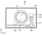
次に、上述した塗布処理装置30〜33の構成について説明する。塗布処理装置30は、図4に示すように内部を密閉可能な処理容器100を有している。処理容器100のウェハ搬送装置20側の側面には、ウェハWの搬入出口(図示せず)が形成され、当該搬入出口には開閉シャッタ(図示せず)が設けられている。
Next, the structure of the
処理容器100内の中央部には、ウェハWを保持して回転させるスピンチャック110が設けられている。スピンチャック110は、水平な上面を有し、当該上面には、例えばウェハWを吸引する吸引口(図示せず)が設けられている。この吸引口からの吸引により、ウェハWをスピンチャック110上に吸着保持できる。
A
スピンチャック110の下方には、例えばモータなどを備えたチャック駆動部111が設けられている。スピンチャック110は、チャック駆動部111により所定の速度に回転できる。また、チャック駆動部111には、例えばシリンダなどの昇降駆動源が設けられており、スピンチャック110は昇降自在になっている。
Below the
スピンチャック110の周囲には、ウェハWから飛散又は落下する液体を受け止め、回収するカップ112が設けられている。カップ112の下面には、回収した液体を排出する排出管113と、カップ112内の雰囲気を真空引きして排気する排気管114が接続されている。
Around the
図5に示すようにカップ112のX方向負方向(図5中の下方向)側には、Y方向(図5中の左右方向)に沿って延伸するレール120が形成されている。レール120は、例えばカップ112のY方向負方向(図5中の左方向)側の外方からY方向正方向(図5中の右方向)側の外方まで形成されている。レール120には、アーム121が取り付けられている。
As shown in FIG. 5, a
アーム121には、図4及び図5に示すようにウェハW上に有機材料を供給する塗布ノズル122が支持されている。アーム121は、図5に示すノズル駆動部123により、レール120上を移動自在である。これにより、塗布ノズル122は、カップ112のY方向正方向側の外方に設置された待機部124からカップ112内のウェハWの中心部上方まで移動でき、さらに当該ウェハW上をウェハWの径方向に移動できる。また、アーム121は、ノズル駆動部123によって昇降自在であり、塗布ノズル122の高さを調節できる。
As shown in FIGS. 4 and 5, the
塗布ノズル122には、図4に示すように当該塗布ノズル122に有機材料を供給する供給管125が接続されている。供給管125は、内部に有機材料を貯留する有機材料供給源126に連通している。また、供給管125には、有機材料の流れを制御するバルブや流量調節部等を含む供給機器群127が設けられている。
As shown in FIG. 4, a
なお、スピンチャック110の下方には、ウェハWの裏面に向けて洗浄液を噴射するバックリンスノズル(図示せず)が設けられていてもよい。このバックリンスノズルから噴射される洗浄液によって、ウェハWの裏面とウェハWの外周部が洗浄される。
A back rinse nozzle (not shown) that sprays the cleaning liquid toward the back surface of the wafer W may be provided below the
なお、塗布処理装置31〜33の構成は、上述した塗布処理装置30の構成と同様であるので説明を省略する。
In addition, since the structure of the coating processing apparatuses 31-33 is the same as that of the
次に、上述したウェハ処理装置40〜42、50〜52の構成について説明する。ウェハ処理装置40は、図6及び図7に示すように内部を閉鎖可能な処理容器130を有している。処理容器130のウェハ搬送装置20側の側面には、ウェハWの搬入出口(図示せず)が形成され、当該搬入出口には開閉シャッタ(図示せず)が設けられている。
Next, the structure of the
処理容器130の天井面には、当該処理容器130の内部に例えば酸化性ガスを供給するガス供給口131が形成されている。ガス供給口131には、ガス供給源132に連通するガス供給管133が接続されている。ガス供給管133には、酸化性ガスの流れを制御するバルブや流量調節部等を含む供給機器群134が設けられている。
A
なお、本実施の形態において酸化性ガスには、通常の大気よりも酸素濃度の高いガスが用いられる。但し、処理容器130の内に特定のガスを供給せずに当該処理容器130の内部を大気雰囲気にしてもよく、かかる場合には、上記ガス供給口131、ガス供給源132、ガス供給管133、供給機器群134を省略してもよい。
In this embodiment, a gas having an oxygen concentration higher than that of normal air is used as the oxidizing gas. However, the inside of the
また、図示の例においては、ガス供給口131は後述する第1の熱処理部140側に設けられているが、紫外線照射部142側に設けられていてもよい。かかる場合、ガス供給口131から酸化性ガスが供給されることによりダウンフローが生じ、後述するように紫外線照射処理によってウェハW上の有機膜の表面を除去する際、有機膜から発生する昇華物等が紫外線照射部142に付着するのを抑制することができる。
In the illustrated example, the
処理容器130の底面には、当該処理容器130の内部の雰囲気を吸引する吸気口135が形成されている。吸気口135には、例えば真空ポンプなどの負圧発生装置136に連通する吸気管137が接続されている。
An
処理容器130の内部には、第1の熱処理部140、他の熱処理部としての第2の熱処理部141、紫外線照射部142とが設けられている。第1の熱処理部140と第2の熱処理部141はY方向に並べて配置され、紫外線照射部142は第2の熱処理部141の上方に配置されている。
Inside the
第1の熱処理部140は、塗布処理装置30〜33においてウェハW上に塗布された有機材料を加熱して、当該ウェハW上に有機膜を形成する。
The first
第1の熱処理部140は、熱板150を収容して熱板150の外周部を保持する環状の保持部材151と、その保持部材151の外周を囲む略筒状のサポートリング152を備えている。熱板150は、厚みのある略円盤形状を有し、ウェハWを載置して加熱することができる。また、熱板150には、例えば加熱機構153が内蔵されている。加熱機構153には、例えばヒータが用いられる。熱板150の加熱温度は例えば制御部200により制御され、熱板150上に載置されたウェハWが所定の温度に加熱される。
The first
熱板150の下方には、ウェハWを下方から支持し昇降させるための昇降ピン160が例えば3本設けられている。昇降ピン160は、昇降駆動部161により上下動できる。熱板150の中央部付近には、当該熱板150を厚み方向に貫通する貫通孔162が例えば3箇所に形成されている。そして、昇降ピン160は貫通孔162を挿通し、熱板150の上面から突出可能になっている。
Below the
第2の熱処理部141は、第1の熱処理部140において熱処理を行った後、紫外線照射部142による紫外線照射処理を行う際に、ウェハW上の有機膜を加熱する。
The second
第2の熱処理部141は、第1の熱処理部140と同様の構成を有している。すなわち、第2の熱処理部141は、熱処理板としての熱板170、保持部材171、サポートリング172、加熱機構173を有している。また熱板170の下方には昇降ピン180、昇降駆動部181が設けられ、熱板170の中央部付近には貫通孔182が形成されている。
The second
紫外線照射部142は、例えば172nmの波長の紫外線を照射する。そして、第1の熱処理部140において熱処理を行った後、紫外線照射部142はウェハW上の有機膜に対して紫外線照射処理を行う。なお、図示の例において紫外線照射部142は処理容器130の天井面に支持されて設けられているが、当該紫外線照射部142は処理容器130の天井面に設けられたガラス窓(図示せず)上に設けられていてもよい。かかる場合、紫外線照射部142から照射された紫外線はガラス窓を介して処理容器130の内部に進入する。
The
なお、処理容器130の内部には、第1の熱処理部140と第2の熱処理部141との間でウェハWを搬送する搬送機構(図示せず)が設けられている。或いは、この搬送機構に代えて、ウェハ搬送装置20によって第1の熱処理部140と第2の熱処理部141との間でウェハWを搬送してもよい。
Note that a transfer mechanism (not shown) for transferring the wafer W between the first
また、ウェハ処理装置41、42、50〜52の構成は、上述したウェハ処理装置40の構成と同様であるので説明を省略する。
Moreover, since the structure of the
以上の成膜システム1には、図1に示すように制御部200が設けられている。制御部200は、例えばコンピュータであり、プログラム格納部(図示せず)を有している。プログラム格納部には、成膜システム1における成膜処理を実行するプログラムが格納されている。なお、前記プログラムは、例えばコンピュータ読み取り可能なハードディスク(HD)、フレキシブルディスク(FD)、コンパクトディスク(CD)、マグネットオプティカルデスク(MO)、メモリーカードなどのコンピュータに読み取り可能な記憶媒体Hに記録されていたものであって、その記憶媒体Hから制御部200にインストールされたものであってもよい。
The above
本実施の形態にかかる成膜システム1は以上のように構成されている。次に、その成膜システム1で行われる有機膜を成膜する処理について説明する。図8は成膜システム1で処理される前のウェハWの状態を示し、図9は成膜処理の各工程におけるウェハWの状態を示している。
The
成膜システム1で処理されるウェハW上には、図8に示すように予めSiO2膜等の所定のパターンPが形成されている。ウェハW上においてパターンPは疎密に形成されており、ウェハW上には、パターンPの窪み部が形成されず、膜(パターンP)がウェハWの表面を覆う第1の領域Aと、パターンP、P間に窪み部Qが形成された第2の領域Bとが形成されている。すなわち、第1の領域Aはいわゆるブランケット領域であり、第2の領域Bは例えばラインアンドスペースのパターンPが形成された領域である。
A predetermined pattern P such as a SiO 2 film is formed in advance on the wafer W to be processed by the
先ず、ウェハ搬送体12によって、カセット載置台10上のカセットCからウェハWが取り出され、処理ステーション3の受け渡し装置21に搬送される。その後、ウェハWは、ウェハ搬送装置20によって温度調節装置43に搬送され、所定の温度に温度調節される。
First, the wafer W is taken out from the cassette C on the cassette mounting table 10 by the
その後、ウェハWは、ウェハ搬送装置20によって塗布処理装置30に搬送される。塗布処理装置30に搬入されたウェハWは、ウェハ搬送装置20からスピンチャック110に受け渡され吸着保持される。続いて、アーム121によって待機部124の塗布ノズル122をウェハWの中心部の上方まで移動させる。その後、スピンチャック110によってウェハWを回転させながら、塗布ノズル122からウェハW上に有機材料を供給する。供給された有機材料は遠心力によりウェハWの表面全面に拡散されて、当該ウェハW上に有機材料が塗布される(工程S1)。
Thereafter, the wafer W is transferred to the
このとき、図9(a)に示すようにウェハW上に塗布された有機材料Lの表面張力や粘度に起因して、第2の領域Bの有機材料L(以下、「有機材料LB」という。)は、第1の領域Aの有機材料L(以下、「有機材料LA」という。)に比べて窪む。すなわち、有機材料LBのパターンP表面からの高さHB1は、有機材料LAのパターンP表面からの高さHA1より低くなる。そして、有機材料LAと有機材料LBとの間で段差D1が生じる。 At this time, as shown in FIG. 9A, due to the surface tension and viscosity of the organic material L applied on the wafer W, the organic material L in the second region B (hereinafter referred to as “organic material L B ”). Is recessed compared to the organic material L in the first region A (hereinafter referred to as “organic material L A ”). That is, the height H B1 from the pattern P the surface of the organic material L B is lower than the height H A1 from pattern P the surface of the organic material L A. Then, step D 1 occurs between the organic material L A and an organic material L B.
その後、ウェハWは、ウェハ搬送装置20によってウェハ処理装置40に搬送される。このとき、ウェハ処理装置40の内部は、酸化性ガスの常圧雰囲気に維持されている。ウェハ処理装置40に搬入されたウェハWは、先ず第1の熱処理部140に搬送され、予め上昇して待機していた昇降ピン160に受け渡される。続いて昇降ピン160が下降して、ウェハWは熱板150上に載置される。そして熱板150上のウェハWは、所定の温度、例えば300℃に加熱される。ウェハWが所定の時間加熱されると、ウェハW上の有機材料Lが加熱されて、図9(b)に示すようにウェハW上に有機膜Fが形成される(工程S2)。なお、第1の領域Aの有機膜F(以下、「有機膜FA」という場合がある。)と第2の領域Bの有機膜F(以下、「有機膜FB」という場合がある。)との間には、上述した段差D1が生じている。
Thereafter, the wafer W is transferred to the
その後、ウェハWは第2の熱処理部141に搬送され、予め上昇して待機していた昇降ピン180に受け渡される。続いて昇降ピン180が下降して、ウェハWは熱板170上に載置される。そして熱板170上のウェハWは、所定の温度、例えば300℃に加熱される。
Thereafter, the wafer W is transferred to the second
また、ウェハWが熱板170上に載置されると、紫外線照射部142から172nmの波長の紫外線を照射する。照射された紫外線によって、処理容器130内の酸化性ガスの処理雰囲気中に活性酸素とオゾンが発生する。これら活性酸素とオゾンによって、有機膜Fの表面が分解されて除去される(工程S3)。すなわち、有機膜Fのエッチバックが行われる。
Further, when the wafer W is placed on the
このように有機膜Fの表面の除去は、熱板170によって有機膜Fを加熱しながら、紫外線照射部142から紫外線を照射することで行われる。そして、図9(c)に示すように有機膜Fの表面の除去は、有機膜FAが完全に除去される所定の深さまで、すなわち高さHA1分の有機膜Fの表面が除去される。そうすると、パターンPの表面が露出し、第1の領域Aには有機膜FAが存在せず、第2の領域BにおいてパターンPの窪み部Q内に高さHC1(=HA1−HB1)の有機膜FBが残存する。
Thus, the removal of the surface of the organic film F is performed by irradiating ultraviolet rays from the
なお、紫外線照射部142による紫外線処理を行う際、有機膜Fを加熱することによって、有機膜Fの表面の除去を短時間で効率よく行うことができる。例えば常温(23℃)の有機膜Fの表面を100nm除去する場合、紫外線照射処理を10分間行う必要があるのに対し、本実施の形態のように300℃で有機膜Fを加熱しながら当該有機膜Fの表面を100nm除去する場合、紫外線照射処理は30秒間行うだけでよい。
In addition, when performing the ultraviolet treatment by the
また、紫外線照射部142から照射する紫外線の波長は、特に限定されるものではないが、本実施の形態のように172nmが好ましい。紫外線の波長が短いほど、紫外線照射処理を行う際のパワーが大きく、効率よく有機膜Fの表面を除去することができるが、当該波長の短い紫外線は処理容器130内に存在する物質に吸収され易くなる。そこで、有機膜Fの表面を除去する効率と物質に吸収され難さとのバランスを考慮し、紫外線の波長は172nmが好ましい。
Further, the wavelength of the ultraviolet light irradiated from the
その後、ウェハWは、ウェハ搬送装置20によって温度調節装置44に搬送され、所定の温度に温度調節される。
Thereafter, the wafer W is transferred to the
以上のように工程S1におけるウェハW上への有機材料Lの塗布処理、工程S2におけるウェハW上の有機材料Lの加熱処理、工程S3におけるウェハW上の有機膜Fの表面除去処理が順次行われて、ウェハW上に有機膜Fが形成される。そして、これら工程S1〜S3が複数回、例えばn回行われる。なお、各回の工程S3後には温度調節装置43、44、53、54におけるウェハWの温度調節が行われるが、以下においては説明を省略する。
As described above, the coating process of the organic material L on the wafer W in the process S1, the heating process of the organic material L on the wafer W in the process S2, and the surface removal process of the organic film F on the wafer W in the process S3 are sequentially performed. As a result, the organic film F is formed on the wafer W. And these processes S1-S3 are performed in multiple times, for example, n times. In addition, although temperature control of the wafer W in the
次に2回目の工程S1〜S3について説明する。なお、2回目の工程S1〜S3は、それぞれ1回目の工程S1〜S3と同様の工程であり、以下の説明では要点のみについて説明する。 Next, the second steps S1 to S3 will be described. The second processes S1 to S3 are the same processes as the first processes S1 to S3, respectively, and only the main points will be described in the following description.
2回目の工程S1では、塗布処理装置31においてウェハW上に有機材料Lが塗布される。この2回目の工程S1においては、1回目の工程S1に比べて、有機材料Lが小さい膜厚で塗布される。具体的には、例えばスピンチャック110の回転数を大きくする、或いはウェハW上に供給する有機材料Lの供給量を少なくする等を行い、2回目の有機材料Lの膜厚を1回目の有機材料Lの膜厚より小さくする。そして、後述する図9(d)に示すように2回目の有機膜FA、FB(有機材料LA、LB)の高さHA2、HB2は、1回目の有機膜FA、FBの高さHA1、HB1よりも小さくなる。
In the second step S <b> 1, the organic material L is applied onto the wafer W in the
その後、2回目の工程S2では、ウェハ処理装置41の第1の熱処理部140においてウェハW上の有機材料Lが加熱されて、図9(d)に示すようにウェハW上に有機膜Fが形成される。このとき、有機膜FAと有機膜FBとの間には、段差D2が生じている。但し、2回目の工程S1において有機材料Lの膜厚を小さくした分、この段差D2は上述した1回目の段差D1よりも小さくなっている。
Thereafter, in the second step S2, the organic material L on the wafer W is heated in the first
その後、2回目の工程S3では、ウェハ処理装置41の第2の熱処理部141においてウェハW上の有機膜Fを加熱しながら、紫外線照射部142から紫外線を照射することによって、図9(e)に示すように有機膜Fの表面が除去される。有機膜Fの表面の除去は、有機膜FAが完全に除去されるまで、すなわち高さHA2分の有機膜Fの表面が除去される。そうすると、第1の領域Aには有機膜FAが存在せず、第2の領域BにおいてパターンPの窪み部Q内に高さHC2(=HA1−HB1)の有機膜FBが残存する。なお、2回目の工程S3後に残存する有機膜FBの高さHC2は、1回目の工程S3後に残存する有機膜FBの高さHC1よりも大きくなっている。すなわち、工程S1〜S3の回数を重ねるごとに、パターンPの窪み部Qに有機膜FBが溜まっていく。
Thereafter, in the second step S3, the second
以上の2回目の工程S1〜S3と同様に、3回目〜n回目の工程S1〜S3を行う。そうすると、有機膜FAと有機膜FBとの間の段差D3〜Dnは小さくなり、最終的には段差Dnはほぼゼロになる。そうすると、図9(f)に示すように有機膜FBの表面の高さとパターンPの表面の高さが同一になる。なお、段差Dnは完全にゼロでなくとも、要求される所定の範囲内に収まっていればよい。
Similar to the second step S1 to S3, the third to nth steps S1 to S3 are performed. Then,
その後、塗布処理装置32においてウェハW上に所定の膜厚の有機材料Lを塗布し、ウェハ処理装置42の第1の熱処理部140においてウェハW上の有機材料Lを加熱する。こうして、図9(g)に示すようにウェハW上に所定の膜厚であり、且つ表面が平坦化された有機膜Fが形成される。
Thereafter, an organic material L having a predetermined film thickness is applied on the wafer W in the
なお本実施の形態では、有機膜Fの形成に際し、最後に工程S1及びS2を行い有機材料Lを塗布し加熱して終了していたが、工程S3を行い有機膜Fの表面を除去して終了してもよい。いずれの工程で終了するかは、要求される製品の仕様に応じて決定すればよい。また、有機膜Fの表面を除去して終了する場合、有機膜Fの膜厚が所定の膜厚になるように有機膜Fの表面を除去すればよく、例えば図9(g)に示した状態まで有機膜Fの表面を除去してもよい。 In the present embodiment, when the organic film F is formed, the processes S1 and S2 are finally performed and the organic material L is applied and heated. However, the process S3 is performed to remove the surface of the organic film F. You may end. Which process is to be completed may be determined according to the required product specifications. When the process is completed after removing the surface of the organic film F, the surface of the organic film F may be removed so that the film thickness of the organic film F becomes a predetermined film thickness, for example, as shown in FIG. The surface of the organic film F may be removed to the state.
その後、ウェハWは、ウェハ搬送装置20によって受け渡し装置21に搬送され、ウェハ搬送体12によってカセットCに戻される。こうして成膜システム1における一連の成膜処理が終了する。
Thereafter, the wafer W is transferred to the
以上の実施の形態によれば、工程S3において、紫外線照射部142から紫外線を照射することによって処理雰囲気中に活性酸素とオゾンを発生させ、これら活性酸素とオゾンによってウェハW上の有機膜Fの表面を除去することができる。そして、工程S1〜S3を繰り返し行うことによって、有機膜FAと有機膜FBとの間の段差Dnがほぼゼロになり、ウェハW上の有機膜Fの表面を平坦化することができる。その結果、種々の膜厚(例えば数十μm〜数十nm)の有機膜FをウェハW上に形成することができる。
According to the above embodiment, in step S3, active oxygen and ozone are generated in the processing atmosphere by irradiating ultraviolet rays from the
また工程S3では、紫外線照射部142から紫外線を照射する際、熱板170によって有機膜Fを加熱するので、有機膜Fの表面の除去を短時間で効率よく行うことができる。
In step S3, when the ultraviolet ray is irradiated from the ultraviolet
また工程S3では、熱板170によって有機膜Fを加熱しながら、紫外線照射部142から紫外線を照射することによって有機膜Fの表面を除去するので、従来のドライエッチング法を行った場合のようにウェハW、或いはウェハW上のパターンPやLow−K膜等の層間絶縁膜などが損傷を被らず、さらにパターンPや層間絶縁膜などが改質されるおそれもない。したがって、ウェハW上に有機膜Fを適切に形成することができる。
In step S3, the surface of the organic film F is removed by irradiating the ultraviolet ray from the
また有機膜Fの表面を除去するに際し、従来のドライエッチング法を行った場合、表面除去の精度は数nmレベルであった。これに対して、発明者らが鋭意検討した結果、本実施の形態のように工程S3において紫外線照射処理を行う場合、表面除去の精度を0.1nmレベルにできることが分かった。したがって、本実施の形態によれば、有機膜Fの表面除去の精度を向上させることができる。 Further, when removing the surface of the organic film F, when the conventional dry etching method is performed, the accuracy of the surface removal is on the order of several nm. On the other hand, as a result of intensive studies by the inventors, it was found that the accuracy of surface removal can be reduced to the 0.1 nm level when the ultraviolet irradiation process is performed in step S3 as in the present embodiment. Therefore, according to the present embodiment, the accuracy of the surface removal of the organic film F can be improved.
また有機膜Fの表面を除去するに際し、従来のドライエッチング法を行った場合、マイクロローディング効果の影響を受け、パターンPが疎に形成されている部分では表面除去速度(エッチングレート)が大きく、パターンPが密に形成されている部分では表面除去速度が小さくなる。このため、有機膜Fの表面を均一に除去することができず、当該有機膜Fの表面を平坦化することができない。これに対して、本実施の形態のように工程S3では、一様な処理雰囲気中で紫外線照射処理が行われるので、有機膜Fの表面を均一に除去することができる。したがって、有機膜Fの表面を平坦化することができる。 Further, when the conventional dry etching method is performed when removing the surface of the organic film F, the surface removal rate (etching rate) is large in the portion where the pattern P is formed sparsely due to the influence of the microloading effect, In the portion where the pattern P is densely formed, the surface removal speed is reduced. For this reason, the surface of the organic film F cannot be removed uniformly, and the surface of the organic film F cannot be flattened. In contrast, in the step S3 as in the present embodiment, since the ultraviolet irradiation process is performed in a uniform processing atmosphere, the surface of the organic film F can be uniformly removed. Therefore, the surface of the organic film F can be planarized.
さらに本実施の形態によれば、工程S1の有機材料Lの塗布処理、工程S2の有機材料Lの加熱処理、及び工程S3の有機膜Fの表面の除去処理をすべて常圧雰囲気下で行うことができ、これらの工程を一の成膜システム1内で行うことができる。したがって、従来のようにエッチバック法を行い、常圧雰囲気下の処理と真空雰囲気下の処理を別々のシステムで行う場合に比べて、本実施の形態の成膜システム1の製造コストを低廉化することができ、またウェハ処理のスループットを向上させることができる。
Further, according to the present embodiment, the coating process of the organic material L in the step S1, the heating process of the organic material L in the step S2, and the removal process of the surface of the organic film F in the step S3 are all performed under a normal pressure atmosphere. These steps can be performed in one
また本実施の形態によれば、工程S3において有機膜Fの表面を除去する際にパターンP間のスカム(レジスト残差)も除去することができる。さらにパターンP(レジストパターン)のリワークも可能になる。 Moreover, according to this Embodiment, when removing the surface of the organic film F in process S3, the scum (resist residual) between the patterns P can also be removed. Furthermore, rework of the pattern P (resist pattern) is also possible.
なお、以上の実施の形態の工程S3において、有機膜Fの表面の除去速度は、第2の熱処理部141における熱板170による加熱温度で制御される。例えば加熱温度を高くすると、有機膜Fの表面の除去速度が大きくなる。
In step S3 of the above embodiment, the removal speed of the surface of the organic film F is controlled by the heating temperature by the
また有機膜Fの表面の除去速度は、処理雰囲気の酸素濃度、紫外線の照度、紫外線の照射時間でも制御される。例えば処理雰囲気の酸素濃度を大きくすると、処理雰囲気に発生する活性酸素とオゾンが増加し、有機膜Fの表面の除去速度が大きくなる。また紫外線の照度を大きくすると、有機膜Fの表面の除去速度が大きくなる。さらに紫外線の照射時間を長くすると、有機膜Fの表面の除去速度が大きくなる。 The removal rate of the surface of the organic film F is also controlled by the oxygen concentration in the processing atmosphere, the illuminance of ultraviolet rays, and the irradiation time of ultraviolet rays. For example, when the oxygen concentration in the processing atmosphere is increased, active oxygen and ozone generated in the processing atmosphere increase, and the removal rate of the surface of the organic film F increases. Further, when the illuminance of ultraviolet rays is increased, the removal speed of the surface of the organic film F is increased. Furthermore, when the irradiation time of ultraviolet rays is lengthened, the removal speed of the surface of the organic film F increases.
以上の実施の形態において、工程S1〜S3を何回繰り返すかは、例えば要求される有機膜Fの膜厚や段差Dnに要求される所定の範囲等、種々の条件に応じて任意に設定することができる。 In the above embodiment, how many times the steps S1 to S3 are repeated is arbitrarily set according to various conditions such as a required film thickness of the organic film F and a predetermined range required for the step D n. can do.
また以上の実施の形態では、工程S1〜S3を複数回行っていたが、1回目の段差D1が要求される所定の範囲内に収まる場合には、これら工程S1〜S3を1回行うだけでよい。 In addition the above embodiment, although the step S1~S3 had done a plurality of times, if within a predetermined range first step D 1 is required, perform these steps S1~S3 once only It's okay.
以上の実施の形態において、ウェハ処理装置40の内部には第1の熱処理部140と第2の熱処理部141が別々に設けられていたが、図10に示すように第1の熱処理部140を省略し、第2の熱処理部141が第1の熱処理部140を兼用してもよい。かかる場合、工程S2において熱板170によりウェハW上の有機材料Lが加熱される。続いて工程S3において、熱板170によって有機膜Fを加熱しながら、紫外線照射部142から紫外線を照射して有機膜Fの表面が除去される。
In the above embodiment, the first
本実施の形態によれば、第1の熱処理部140を省略できるので、ウェハ処理装置40の製造コストを低廉化できると共に、ウェハ処理装置40の専有面積を小さくすることができる。特に工程S2における加熱温度と工程S3における加熱温度が同じ場合には、熱板170の温度を一定に維持することができるので、かかる場合に本実施の形態は有用である。
According to the present embodiment, since the first
以上の実施の形態において、第1の熱処理部140と第2の熱処理部141は一のウェハ処理装置40内に設けられていたが、個別の装置内に設けられていてもよい。例えば図11に示すように第3の処理ブロックG3に、第1の熱処理部140を備えた熱処理装置300、301、第2の熱処理部141と紫外線照射部142を備えたウェハ処理装置302、303、304を配置してもよい。同様に第4の処理ブロックG4にも、第1の熱処理部140を備えた熱処理装置310、311、第2の熱処理部141と紫外線照射部142を備えたウェハ処理装置312、313、314を配置してもよい。なお図示の例においては、ウェハWの温度を調節する温度調節装置を省略している。
In the above embodiment, the first
上述したように工程S3における有機膜Fの表面の除去速度は、例えば第2の熱処理部141における熱板170による加熱温度で制御される。また、工程S3を複数回行う場合、回数を重ねるに伴い、各回における有機膜Fの膜厚は小さくなり、有機膜FAと有機膜FBとの間の段差Dは小さくなっていくため、各回の工程S3における有機膜Fの表面の除去速度を小さくする場合がある。
As described above, the removal rate of the surface of the organic film F in step S3 is controlled by, for example, the heating temperature by the
そこで本実施の形態では、複数のウェハ処理装置302〜304、312〜314を備えているので、各ウェハ処理装置302〜304、312〜314における熱板170の加熱温度を異なる温度に設定することができる。そうすると本実施の形態は、上述したように各回の工程S3における有機膜Fの表面の除去速度が異なる場合にも適用できる。すなわち、各熱板170の加熱温度を昇降させる必要がなく、各熱板170の加熱温度を一定に維持することができるので、ウェハ処理のスループットをさらに向上させることができる。
Therefore, in this embodiment, since a plurality of wafer processing apparatuses 302 to 304 and 312 to 314 are provided, the heating temperature of the
以上の実施の形態において、工程S3における有機膜Fの加熱処理は熱板170によって行っていたが、当該有機膜Fの加熱処理方法はこれに限定されない。
In the above embodiment, the heat treatment of the organic film F in the step S3 is performed by the
工程S3における有機膜Fの加熱処理に際し、例えば図12に示すように熱板170に代えて、保温材320を用いてもよい。ウェハ処理装置40の第2の熱処理部141には、上記実施の形態の熱板170、保持部材171、サポートリング172、加熱機構173に代えて、保温材320を載置する載置台321が設けられている。載置台321内には上記昇降ピン180、昇降駆動部181が設けられ、載置台321の上面には貫通孔182が形成されている。
In the heat treatment of the organic film F in step S3, for example, a
保温材320はウェハWを保持して保温することができる。保温材320には、熱容量が大きい材料、例えば石英ガラスが用いられる。また保温材320は、移動機構(図示せず)によって、第1の熱処理部140の熱板150と第2の熱処理部141の載置台321上を移動自在に構成されている。なお、ウェハ処理装置40のその他の構成については、上記実施の形態のウェハ処理装置40の構成と同様であるので説明を省略する。
The
かかる場合、工程S2において、第1の熱処理部140の熱板150でウェハWが所定の温度、例えば300℃に加熱される際、保温材320も同じ温度に加熱される。その後、ウェハWは保温材320に保持された状態で載置台321に搬送される。そして、工程S3において紫外線照射部142による紫外線処理を行う際、ウェハWは保温材320によってその温度が保持されている。このため、工程S3においてウェハW上の有機膜Fを加熱しながら、紫外線照射部142から紫外線を照射できる。本実施の形態によれば、上記実施の形態と同様の効果を享受することができ、すなわち、有機膜Fの表面を効率よく除去することができる。
In such a case, in step S2, when the wafer W is heated to a predetermined temperature, for example, 300 ° C., by the
また工程S3における有機膜Fの加熱処理に際し、熱板170に代えて、光源としてのLED(Light Emitting Diode:発光ダイオード)を用いてもよい。例えば図13に示すようにウェハ処理装置40の処理容器130の内部には、ウェハWを載置する載置板330が設けられている。載置板330は、移動機構(図示せず)によって水平方向のY方向に移動可能に構成されている。載置板330の下方には、ウェハWを下方から支持し昇降させるための昇降ピン331が例えば3本設けられている。昇降ピン331は、昇降駆動部332により上下動できる。載置板330の中央部付近には、当該載置板330を厚み方向に貫通する貫通孔333が例えば3箇所に形成されている。そして、昇降ピン331は貫通孔333を挿通し、載置板330の上面から突出可能になっている。
In addition, in the heat treatment of the organic film F in the step S3, an LED (Light Emitting Diode) as a light source may be used instead of the
載置板330の上方には、紫外線照射部340と第2の熱処理部341とが一体になって設けられている。これら紫外線照射部340と第2の熱処理部341は、移動機構(図示せず)によって水平方向のY方向に移動可能に構成されている。
Above the mounting
紫外線照射部340は、紫外線照射部142と同様に172nmの波長の紫外線を照射する。
The
第2の熱処理部341には、複数のLED350がY方向に一列に並べて配置されている。LED350は、ウェハWの径方向の長さより長く設けられている。すなわち、LED350は、載置板330上のウェハWの径方向全体に照射光を発光することができる。
In the second
なお本実施の形態では、成膜システム1に第1の熱処理部140を備えた熱処理装置(図示せず)が別途設けられる。
In the present embodiment, the
かかる場合、工程S3において、ウェハWを載置した載置板330がY方向負方向側に移動すると共に、紫外線照射部340と第2の熱処理部341がY方向正方向側に移動する。すなわち、載置板330と紫外線照射部340が相対的に近づくように移動する。なお本実施の形態では、載置板330と紫外線照射部340及び第2の熱処理部341を共に移動させていたが、いずれか一方を移動させもよい。
In this case, in step S3, the mounting
そして、第2の熱処理部341のLED350から発光される照射光によってウェハW上の有機膜Fを加熱しながら、紫外線照射部340から紫外線を照射する。そうすると、上記実施の形態と同様に有機膜Fの表面が除去される。したがって、本実施の形態によれば、上記実施の形態と同様の効果を享受することができ、すなわち、有機膜Fの表面を効率よく除去することができる。
Then, ultraviolet rays are irradiated from the
なお、以上の実施の形態の工程S3において、有機膜Fの表面の除去速度は、第2の熱処理部341におけるLED350の発光強度、LED350の数、LED350から発光される照射光の波長等によって制御することができる。
In step S3 of the above embodiment, the removal rate of the surface of the organic film F is controlled by the light emission intensity of the
また、上述したように工程S3を複数回行う場合、各回の有機膜Fの表面の除去速度を小さくする場合がある。かかる場合であっても、LED350の発光強度を制御し、LED350のオンオフを制御してその数を制御し、LED350から発光される照射光の波長を制御することで、有機膜Fの表面の除去速度を制御することができる。またLED350の反応速度が速いため、有機膜Fの加熱温度の昇降温を容易に制御することができ、又有機膜Fの加熱温度の昇降温を局所的に制御することもできる。したがって、より効率よく有機膜Fの表面を除去することができる。
Further, as described above, when the step S3 is performed a plurality of times, the removal rate of the surface of the organic film F may be reduced each time. Even in such a case, the surface of the organic film F can be removed by controlling the emission intensity of the
なお、以上の実施の形態では、第2の熱処理部341における光源としてLED350を用いたが、LED350に代えて、例えばレーザやハロゲンランプ等、種々の光源を用いることもできる。
In the above embodiment, the
以上の実施の形態において、成膜システム1は、ウェハW上に所定の有機膜Fを形成した後、当該有機膜Fの膜厚を測定する膜厚測定部としての膜厚測定装置を有していてもよい。膜厚測定装置は、成膜システム1内において例えば受け渡し装置21上に積層されて設けられる。
In the above embodiment, the
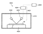
図14に示すように膜厚測定装置400は、処理容器410を有している。処理容器410のウェハ搬送装置20側の側面には、ウェハWの搬入出口(図示せず)が形成され、当該搬入出口には開閉シャッタ(図示せず)が設けられている。
As shown in FIG. 14, the film
処理容器410内の底面には、ウェハWを載置する載置台420と、光学式表面形状測定計421が設けられている。載置台420は、例えば水平方向の2次元方向に移動できる。光学式表面形状測定計421は、例えばウェハWに対して斜方向から光を照射する光照射部422と、光照射部422から照射されウェハWで反射した光を検出する光検出部423と、当該光検出部423の受光情報に基づいてウェハW上の有機膜Fの膜厚を算出する測定部424を備えている。膜厚測定装置400は、例えばスキャトロメトリ法を用いて有機膜Fの膜厚を測定するものであり、測定部424において、光検出部423により検出されたウェハ面内の光強度分布と、予め記憶されている仮想の光強度分布とを照合し、その照合された仮想の光強度分布に対応する有機膜Fの膜厚を求めることにより、有機膜Fの膜厚を測定できる。
On the bottom surface in the
かかる場合、膜厚測定装置400では、先ずウェハWが載置台420に載置される。続いてウェハWに光照射部422から光が照射され、その反射光が光検出部423により検出される。そして測定部424において、ウェハW上の有機膜Fの膜厚が測定される。この有機膜Fの膜厚測定結果は、制御部200に出力される。
In such a case, in the film
有機膜Fの膜厚測定結果に基づいて、有機膜Fの膜厚が所定の膜厚になっており、有機膜Fが平坦化されている、すなわち有機膜Fにおける段差Dが所定の範囲内にある場合、以後のウェハWに対してもそのままの処理条件でウェハ処理が行われる。 Based on the film thickness measurement result of the organic film F, the film thickness of the organic film F is a predetermined film thickness, and the organic film F is flattened, that is, the step D in the organic film F is within a predetermined range. In this case, the wafer processing is performed on the subsequent wafer W under the same processing conditions.
一方、有機膜Fが十分に平坦化されていない場合、工程S3における処理条件を補正する。具体的には、例えば第2の熱処理部141、341の加熱温度を補正する。また、紫外線照射部142、340からの紫外線の照度、紫外線の照射時間等の処理条件を補正する。さらに、工程S3の処理雰囲気の酸素濃度を補正する。
On the other hand, when the organic film F is not sufficiently planarized, the processing conditions in step S3 are corrected. Specifically, for example, the heating temperature of the second
本実施の形態によれば、より適切な条件でウェハ処理を行うことができるので、ウェハW上に有機膜Fをより適切に形成することができる。 According to the present embodiment, since the wafer processing can be performed under more appropriate conditions, the organic film F can be more appropriately formed on the wafer W.
なお、以上の実施の形態の工程S3では、有機膜Fを加熱しながら紫外線照射処理を行っていたが、発明者らが鋭意検討した結果、紫外線照射処理のみを行っても、有機膜Fの表面を適切に除去できることが分かっている。 In step S3 of the above embodiment, the ultraviolet irradiation treatment is performed while heating the organic film F. However, as a result of the intensive studies by the inventors, the organic film F can be formed even if only the ultraviolet irradiation treatment is performed. It has been found that the surface can be removed properly.
以上、添付図面を参照しながら本発明の好適な実施の形態について説明したが、本発明はかかる例に限定されない。当業者であれば、特許請求の範囲に記載された思想の範疇内において、各種の変更例または修正例に想到し得ることは明らかであり、それらについても当然に本発明の技術的範囲に属するものと了解される。 The preferred embodiments of the present invention have been described above with reference to the accompanying drawings, but the present invention is not limited to such examples. It is obvious for those skilled in the art that various modifications or modifications can be conceived within the scope of the idea described in the claims, and these naturally belong to the technical scope of the present invention. It is understood.
1 成膜システム
30〜33 塗布処理装置
40〜42、50〜52 ウェハ処理装置
140 第1の熱処理部
141 第2の熱処理部
142 紫外線照射部
150 熱板
170 熱板
200 制御部
300、301、310、311 熱処理装置
302〜304、312〜314 ウェハ処理装置
320 保温材
340 紫外線照射部
341 第2の熱処理部
350 LED
400 膜厚測定装置
A 第1の領域
B 第2の領域
D 段差
F 有機膜
FA (第1の領域Aの)有機膜
FB (第2の領域Bの)有機膜
L 有機材料
LA (第1の領域Aの)有機材料
LB (第2の領域Bの)有機材料
P パターン
Q 窪み部
W ウェハ
DESCRIPTION OF
400 Film Thickness Measuring Device A First Area B Second Area D Step F Organic Film F A Organic Film F B (First Area A) Organic Film L B (Second Area B) Organic Film L Organic Material L A ( Organic material L B (first region A) Organic material P (second region B) P pattern Q Depressed portion W Wafer
Claims (19)
基板上に有機材料を塗布する塗布処理工程と、
その後、前記有機材料を熱処理して基板上に有機膜を形成する熱処理工程と、
その後、前記有機膜に対して紫外線照射処理を行い、当該有機膜の表面を所定の深さまで除去する紫外線照射工程と、を有することを特徴とする、成膜方法。 A film forming method for forming an organic film on a substrate having a pattern formed on a surface thereof,
A coating process for coating an organic material on the substrate;
Thereafter, a heat treatment step of heat-treating the organic material to form an organic film on the substrate;
Then, an ultraviolet irradiation process is performed to perform ultraviolet irradiation treatment on the organic film and remove the surface of the organic film to a predetermined depth.
少なくとも最後より前に行われる前記紫外線照射工程において、前記パターンの表面が露出するまで、前記有機膜の表面を除去することを特徴とする、請求項1に記載の成膜方法。 The coating treatment step, the heat treatment step and the ultraviolet irradiation step are each performed a plurality of times in this order,
2. The film forming method according to claim 1, wherein the surface of the organic film is removed until the surface of the pattern is exposed in the ultraviolet irradiation step performed at least before the last.
前記膜厚測定工程における測定結果に基づいて、前記紫外線照射工程の処理条件を補正することを特徴とする、請求項1〜7のいずれかに記載の成膜方法。 After the ultraviolet irradiation step, further comprising a film thickness measurement step for measuring the film thickness of the organic film,
The film forming method according to claim 1, wherein processing conditions of the ultraviolet irradiation step are corrected based on a measurement result in the film thickness measuring step.
基板上に有機材料を塗布処理する塗布処理部と、
前記有機材料を熱処理して基板上に有機膜を形成する熱処理部と、
前記有機膜に対して紫外線照射処理を行う紫外線照射部と、
前記塗布処理、前記熱処理及び前記紫外線照射処理をこの順で行い、前記紫外線照射処理において前記有機膜の表面を所定の深さまで除去するように、前記塗布処理部、前記熱処理部及び前記紫外線照射部を制御する制御部と、を有することを特徴とする、成膜システム。 A film forming system for forming an organic film on a substrate having a pattern formed on a surface thereof,
An application processing unit for applying an organic material on the substrate;
A heat treatment part for heat-treating the organic material to form an organic film on the substrate;
An ultraviolet irradiation unit for performing an ultraviolet irradiation process on the organic film;
The coating treatment unit, the heat treatment unit, and the ultraviolet ray irradiation unit are performed in this order, and the coating treatment unit, the heat treatment unit, and the ultraviolet ray irradiation unit are configured to remove the surface of the organic film to a predetermined depth in the ultraviolet ray irradiation treatment. And a control unit for controlling the film forming system.
当該装置内には、前記熱処理部と前記紫外線照射部との間を移動自在で、且つ基板を保持して保温する保温材が設けられていることを特徴とする、請求項11又は12に記載の成膜システム。 The heat treatment part and the ultraviolet irradiation part are provided in the same apparatus,
The apparatus is provided with a heat insulating material that is movable between the heat treatment section and the ultraviolet irradiation section and that retains the substrate and retains the temperature. Film formation system.
前記制御部は、前記膜厚測定部による測定結果に基づいて、前記紫外線照射処理の処理条件を補正することを特徴とする、請求項11〜18のいずれかに記載の成膜システム。 It further has a film thickness measuring unit for measuring the film thickness of the organic film subjected to the ultraviolet irradiation treatment,
The film forming system according to claim 11, wherein the control unit corrects a processing condition of the ultraviolet irradiation processing based on a measurement result by the film thickness measuring unit.
Priority Applications (7)
| Application Number | Priority Date | Filing Date | Title |
|---|---|---|---|
| JP2013033216A JP5934665B2 (en) | 2013-02-22 | 2013-02-22 | Film forming method, program, computer storage medium, and film forming system |
| US14/764,687 US9741559B2 (en) | 2013-02-22 | 2014-01-23 | Film forming method, computer storage medium, and film forming system |
| CN201480009698.1A CN105074883B (en) | 2013-02-22 | 2014-01-23 | Film build method and film-forming system |
| PCT/JP2014/051361 WO2014129259A1 (en) | 2013-02-22 | 2014-01-23 | Film-forming method, computer storage medium, and film-forming system |
| KR1020157022381A KR101959108B1 (en) | 2013-02-22 | 2014-01-23 | Film-forming method, computer storage medium, and film-forming system |
| TW105138170A TWI598703B (en) | 2013-02-22 | 2014-02-14 | Film deposition method, computer storage medium, and film deposition system |
| TW103104953A TWI565533B (en) | 2013-02-22 | 2014-02-14 | Film deposition method, computer storage medium, and film deposition system |
Applications Claiming Priority (1)
| Application Number | Priority Date | Filing Date | Title |
|---|---|---|---|
| JP2013033216A JP5934665B2 (en) | 2013-02-22 | 2013-02-22 | Film forming method, program, computer storage medium, and film forming system |
Related Child Applications (1)
| Application Number | Title | Priority Date | Filing Date |
|---|---|---|---|
| JP2016093649A Division JP6149139B2 (en) | 2016-05-09 | 2016-05-09 | Film forming method, program, computer storage medium, and film forming system |
Publications (3)
| Publication Number | Publication Date |
|---|---|
| JP2014165252A true JP2014165252A (en) | 2014-09-08 |
| JP2014165252A5 JP2014165252A5 (en) | 2015-03-05 |
| JP5934665B2 JP5934665B2 (en) | 2016-06-15 |
Family
ID=51391055
Family Applications (1)
| Application Number | Title | Priority Date | Filing Date |
|---|---|---|---|
| JP2013033216A Active JP5934665B2 (en) | 2013-02-22 | 2013-02-22 | Film forming method, program, computer storage medium, and film forming system |
Country Status (6)
| Country | Link |
|---|---|
| US (1) | US9741559B2 (en) |
| JP (1) | JP5934665B2 (en) |
| KR (1) | KR101959108B1 (en) |
| CN (1) | CN105074883B (en) |
| TW (2) | TWI565533B (en) |
| WO (1) | WO2014129259A1 (en) |
Cited By (8)
| Publication number | Priority date | Publication date | Assignee | Title |
|---|---|---|---|---|
| CN105499069A (en) * | 2014-10-10 | 2016-04-20 | 住友重机械工业株式会社 | Film forming apparatus and film forming method |
| KR20160075344A (en) | 2014-12-19 | 2016-06-29 | 도쿄엘렉트론가부시키가이샤 | Substrate processing apparatus and substrate processing method |
| KR20160079691A (en) | 2014-12-26 | 2016-07-06 | 도쿄엘렉트론가부시키가이샤 | Substrate processing method, storage medium and heating apparatus |
| WO2016196739A1 (en) * | 2015-06-02 | 2016-12-08 | Tokyo Electron Limited | Techniques for Spin-on-Carbon Planarization |
| KR20170018787A (en) * | 2015-08-10 | 2017-02-20 | 도오꾜오까고오교 가부시끼가이샤 | Uv irradiation apparatus, resist pattern forming apparatus, uv irradiation method and resist pattern forming method |
| US9874812B2 (en) | 2015-01-30 | 2018-01-23 | Samsung Electronics Co., Ltd. | Methods of forming hardmask material film |
| WO2018146981A1 (en) * | 2017-02-07 | 2018-08-16 | 東京エレクトロン株式会社 | Film forming system, film forming method, and computer storage medium |
| KR20180138139A (en) | 2017-06-19 | 2018-12-28 | 도쿄엘렉트론가부시키가이샤 | Film forming method, storage medium, and film forming system |
Families Citing this family (318)
| Publication number | Priority date | Publication date | Assignee | Title |
|---|---|---|---|---|
| US10378106B2 (en) | 2008-11-14 | 2019-08-13 | Asm Ip Holding B.V. | Method of forming insulation film by modified PEALD |
| US9394608B2 (en) | 2009-04-06 | 2016-07-19 | Asm America, Inc. | Semiconductor processing reactor and components thereof |
| US8802201B2 (en) | 2009-08-14 | 2014-08-12 | Asm America, Inc. | Systems and methods for thin-film deposition of metal oxides using excited nitrogen-oxygen species |
| US9312155B2 (en) | 2011-06-06 | 2016-04-12 | Asm Japan K.K. | High-throughput semiconductor-processing apparatus equipped with multiple dual-chamber modules |
| US10364496B2 (en) | 2011-06-27 | 2019-07-30 | Asm Ip Holding B.V. | Dual section module having shared and unshared mass flow controllers |
| US10854498B2 (en) | 2011-07-15 | 2020-12-01 | Asm Ip Holding B.V. | Wafer-supporting device and method for producing same |
| US20130023129A1 (en) | 2011-07-20 | 2013-01-24 | Asm America, Inc. | Pressure transmitter for a semiconductor processing environment |
| US9017481B1 (en) | 2011-10-28 | 2015-04-28 | Asm America, Inc. | Process feed management for semiconductor substrate processing |
| US9659799B2 (en) | 2012-08-28 | 2017-05-23 | Asm Ip Holding B.V. | Systems and methods for dynamic semiconductor process scheduling |
| US10714315B2 (en) | 2012-10-12 | 2020-07-14 | Asm Ip Holdings B.V. | Semiconductor reaction chamber showerhead |
| US20160376700A1 (en) | 2013-02-01 | 2016-12-29 | Asm Ip Holding B.V. | System for treatment of deposition reactor |
| US9589770B2 (en) | 2013-03-08 | 2017-03-07 | Asm Ip Holding B.V. | Method and systems for in-situ formation of intermediate reactive species |
| US9484191B2 (en) | 2013-03-08 | 2016-11-01 | Asm Ip Holding B.V. | Pulsed remote plasma method and system |
| US9240412B2 (en) | 2013-09-27 | 2016-01-19 | Asm Ip Holding B.V. | Semiconductor structure and device and methods of forming same using selective epitaxial process |
| US10683571B2 (en) | 2014-02-25 | 2020-06-16 | Asm Ip Holding B.V. | Gas supply manifold and method of supplying gases to chamber using same |
| US10167557B2 (en) | 2014-03-18 | 2019-01-01 | Asm Ip Holding B.V. | Gas distribution system, reactor including the system, and methods of using the same |
| US11015245B2 (en) | 2014-03-19 | 2021-05-25 | Asm Ip Holding B.V. | Gas-phase reactor and system having exhaust plenum and components thereof |
| US10858737B2 (en) | 2014-07-28 | 2020-12-08 | Asm Ip Holding B.V. | Showerhead assembly and components thereof |
| US9890456B2 (en) | 2014-08-21 | 2018-02-13 | Asm Ip Holding B.V. | Method and system for in situ formation of gas-phase compounds |
| US10941490B2 (en) | 2014-10-07 | 2021-03-09 | Asm Ip Holding B.V. | Multiple temperature range susceptor, assembly, reactor and system including the susceptor, and methods of using the same |
| US9657845B2 (en) | 2014-10-07 | 2017-05-23 | Asm Ip Holding B.V. | Variable conductance gas distribution apparatus and method |
| KR102263121B1 (en) | 2014-12-22 | 2021-06-09 | 에이에스엠 아이피 홀딩 비.브이. | Semiconductor device and manufacuring method thereof |
| US10529542B2 (en) | 2015-03-11 | 2020-01-07 | Asm Ip Holdings B.V. | Cross-flow reactor and method |
| US10276355B2 (en) | 2015-03-12 | 2019-04-30 | Asm Ip Holding B.V. | Multi-zone reactor, system including the reactor, and method of using the same |
| US10458018B2 (en) | 2015-06-26 | 2019-10-29 | Asm Ip Holding B.V. | Structures including metal carbide material, devices including the structures, and methods of forming same |
| US10600673B2 (en) | 2015-07-07 | 2020-03-24 | Asm Ip Holding B.V. | Magnetic susceptor to baseplate seal |
| US10083836B2 (en) | 2015-07-24 | 2018-09-25 | Asm Ip Holding B.V. | Formation of boron-doped titanium metal films with high work function |
| JP6596257B2 (en) * | 2015-08-03 | 2019-10-23 | 東京応化工業株式会社 | Ultraviolet irradiation apparatus and ultraviolet irradiation method |
| US9960072B2 (en) | 2015-09-29 | 2018-05-01 | Asm Ip Holding B.V. | Variable adjustment for precise matching of multiple chamber cavity housings |
| US10211308B2 (en) | 2015-10-21 | 2019-02-19 | Asm Ip Holding B.V. | NbMC layers |
| US10322384B2 (en) | 2015-11-09 | 2019-06-18 | Asm Ip Holding B.V. | Counter flow mixer for process chamber |
| US11139308B2 (en) | 2015-12-29 | 2021-10-05 | Asm Ip Holding B.V. | Atomic layer deposition of III-V compounds to form V-NAND devices |
| US10468251B2 (en) | 2016-02-19 | 2019-11-05 | Asm Ip Holding B.V. | Method for forming spacers using silicon nitride film for spacer-defined multiple patterning |
| US10529554B2 (en) | 2016-02-19 | 2020-01-07 | Asm Ip Holding B.V. | Method for forming silicon nitride film selectively on sidewalls or flat surfaces of trenches |
| US10501866B2 (en) | 2016-03-09 | 2019-12-10 | Asm Ip Holding B.V. | Gas distribution apparatus for improved film uniformity in an epitaxial system |
| US10343920B2 (en) | 2016-03-18 | 2019-07-09 | Asm Ip Holding B.V. | Aligned carbon nanotubes |
| US9892913B2 (en) | 2016-03-24 | 2018-02-13 | Asm Ip Holding B.V. | Radial and thickness control via biased multi-port injection settings |
| US10190213B2 (en) | 2016-04-21 | 2019-01-29 | Asm Ip Holding B.V. | Deposition of metal borides |
| US10865475B2 (en) | 2016-04-21 | 2020-12-15 | Asm Ip Holding B.V. | Deposition of metal borides and silicides |
| US10032628B2 (en) | 2016-05-02 | 2018-07-24 | Asm Ip Holding B.V. | Source/drain performance through conformal solid state doping |
| US10367080B2 (en) | 2016-05-02 | 2019-07-30 | Asm Ip Holding B.V. | Method of forming a germanium oxynitride film |
| KR102592471B1 (en) | 2016-05-17 | 2023-10-20 | 에이에스엠 아이피 홀딩 비.브이. | Method of forming metal interconnection and method of fabricating semiconductor device using the same |
| US11453943B2 (en) | 2016-05-25 | 2022-09-27 | Asm Ip Holding B.V. | Method for forming carbon-containing silicon/metal oxide or nitride film by ALD using silicon precursor and hydrocarbon precursor |
| US10388509B2 (en) | 2016-06-28 | 2019-08-20 | Asm Ip Holding B.V. | Formation of epitaxial layers via dislocation filtering |
| US9859151B1 (en) | 2016-07-08 | 2018-01-02 | Asm Ip Holding B.V. | Selective film deposition method to form air gaps |
| US10612137B2 (en) | 2016-07-08 | 2020-04-07 | Asm Ip Holdings B.V. | Organic reactants for atomic layer deposition |
| US10714385B2 (en) | 2016-07-19 | 2020-07-14 | Asm Ip Holding B.V. | Selective deposition of tungsten |
| KR102354490B1 (en) | 2016-07-27 | 2022-01-21 | 에이에스엠 아이피 홀딩 비.브이. | Method of processing a substrate |
| US9812320B1 (en) | 2016-07-28 | 2017-11-07 | Asm Ip Holding B.V. | Method and apparatus for filling a gap |
| KR102532607B1 (en) | 2016-07-28 | 2023-05-15 | 에이에스엠 아이피 홀딩 비.브이. | Substrate processing apparatus and method of operating the same |
| US10395919B2 (en) | 2016-07-28 | 2019-08-27 | Asm Ip Holding B.V. | Method and apparatus for filling a gap |
| US9887082B1 (en) | 2016-07-28 | 2018-02-06 | Asm Ip Holding B.V. | Method and apparatus for filling a gap |
| US10410943B2 (en) | 2016-10-13 | 2019-09-10 | Asm Ip Holding B.V. | Method for passivating a surface of a semiconductor and related systems |
| US10643826B2 (en) | 2016-10-26 | 2020-05-05 | Asm Ip Holdings B.V. | Methods for thermally calibrating reaction chambers |
| US11532757B2 (en) | 2016-10-27 | 2022-12-20 | Asm Ip Holding B.V. | Deposition of charge trapping layers |
| US10229833B2 (en) | 2016-11-01 | 2019-03-12 | Asm Ip Holding B.V. | Methods for forming a transition metal nitride film on a substrate by atomic layer deposition and related semiconductor device structures |
| US10643904B2 (en) | 2016-11-01 | 2020-05-05 | Asm Ip Holdings B.V. | Methods for forming a semiconductor device and related semiconductor device structures |
| US10435790B2 (en) | 2016-11-01 | 2019-10-08 | Asm Ip Holding B.V. | Method of subatmospheric plasma-enhanced ALD using capacitively coupled electrodes with narrow gap |
| US10714350B2 (en) | 2016-11-01 | 2020-07-14 | ASM IP Holdings, B.V. | Methods for forming a transition metal niobium nitride film on a substrate by atomic layer deposition and related semiconductor device structures |
| US10134757B2 (en) | 2016-11-07 | 2018-11-20 | Asm Ip Holding B.V. | Method of processing a substrate and a device manufactured by using the method |
| KR102546317B1 (en) | 2016-11-15 | 2023-06-21 | 에이에스엠 아이피 홀딩 비.브이. | Gas supply unit and substrate processing apparatus including the same |
| US10340135B2 (en) | 2016-11-28 | 2019-07-02 | Asm Ip Holding B.V. | Method of topologically restricted plasma-enhanced cyclic deposition of silicon or metal nitride |
| KR20180068582A (en) | 2016-12-14 | 2018-06-22 | 에이에스엠 아이피 홀딩 비.브이. | Substrate processing apparatus |
| US11581186B2 (en) | 2016-12-15 | 2023-02-14 | Asm Ip Holding B.V. | Sequential infiltration synthesis apparatus |
| US11447861B2 (en) | 2016-12-15 | 2022-09-20 | Asm Ip Holding B.V. | Sequential infiltration synthesis apparatus and a method of forming a patterned structure |
| KR102700194B1 (en) | 2016-12-19 | 2024-08-28 | 에이에스엠 아이피 홀딩 비.브이. | Substrate processing apparatus |
| US10269558B2 (en) | 2016-12-22 | 2019-04-23 | Asm Ip Holding B.V. | Method of forming a structure on a substrate |
| US10867788B2 (en) | 2016-12-28 | 2020-12-15 | Asm Ip Holding B.V. | Method of forming a structure on a substrate |
| US11390950B2 (en) | 2017-01-10 | 2022-07-19 | Asm Ip Holding B.V. | Reactor system and method to reduce residue buildup during a film deposition process |
| US10655221B2 (en) | 2017-02-09 | 2020-05-19 | Asm Ip Holding B.V. | Method for depositing oxide film by thermal ALD and PEALD |
| US10468261B2 (en) | 2017-02-15 | 2019-11-05 | Asm Ip Holding B.V. | Methods for forming a metallic film on a substrate by cyclical deposition and related semiconductor device structures |
| US10529563B2 (en) | 2017-03-29 | 2020-01-07 | Asm Ip Holdings B.V. | Method for forming doped metal oxide films on a substrate by cyclical deposition and related semiconductor device structures |
| US10283353B2 (en) | 2017-03-29 | 2019-05-07 | Asm Ip Holding B.V. | Method of reforming insulating film deposited on substrate with recess pattern |
| US10103040B1 (en) | 2017-03-31 | 2018-10-16 | Asm Ip Holding B.V. | Apparatus and method for manufacturing a semiconductor device |
| KR102457289B1 (en) | 2017-04-25 | 2022-10-21 | 에이에스엠 아이피 홀딩 비.브이. | Method for depositing a thin film and manufacturing a semiconductor device |
| US10446393B2 (en) | 2017-05-08 | 2019-10-15 | Asm Ip Holding B.V. | Methods for forming silicon-containing epitaxial layers and related semiconductor device structures |
| US10892156B2 (en) | 2017-05-08 | 2021-01-12 | Asm Ip Holding B.V. | Methods for forming a silicon nitride film on a substrate and related semiconductor device structures |
| US10770286B2 (en) | 2017-05-08 | 2020-09-08 | Asm Ip Holdings B.V. | Methods for selectively forming a silicon nitride film on a substrate and related semiconductor device structures |
| US10504742B2 (en) | 2017-05-31 | 2019-12-10 | Asm Ip Holding B.V. | Method of atomic layer etching using hydrogen plasma |
| US10886123B2 (en) | 2017-06-02 | 2021-01-05 | Asm Ip Holding B.V. | Methods for forming low temperature semiconductor layers and related semiconductor device structures |
| US12040200B2 (en) | 2017-06-20 | 2024-07-16 | Asm Ip Holding B.V. | Semiconductor processing apparatus and methods for calibrating a semiconductor processing apparatus |
| US11306395B2 (en) | 2017-06-28 | 2022-04-19 | Asm Ip Holding B.V. | Methods for depositing a transition metal nitride film on a substrate by atomic layer deposition and related deposition apparatus |
| US10685834B2 (en) | 2017-07-05 | 2020-06-16 | Asm Ip Holdings B.V. | Methods for forming a silicon germanium tin layer and related semiconductor device structures |
| KR20190009245A (en) | 2017-07-18 | 2019-01-28 | 에이에스엠 아이피 홀딩 비.브이. | Methods for forming a semiconductor device structure and related semiconductor device structures |
| US11018002B2 (en) | 2017-07-19 | 2021-05-25 | Asm Ip Holding B.V. | Method for selectively depositing a Group IV semiconductor and related semiconductor device structures |
| US11374112B2 (en) | 2017-07-19 | 2022-06-28 | Asm Ip Holding B.V. | Method for depositing a group IV semiconductor and related semiconductor device structures |
| US10541333B2 (en) | 2017-07-19 | 2020-01-21 | Asm Ip Holding B.V. | Method for depositing a group IV semiconductor and related semiconductor device structures |
| US10605530B2 (en) | 2017-07-26 | 2020-03-31 | Asm Ip Holding B.V. | Assembly of a liner and a flange for a vertical furnace as well as the liner and the vertical furnace |
| US10312055B2 (en) | 2017-07-26 | 2019-06-04 | Asm Ip Holding B.V. | Method of depositing film by PEALD using negative bias |
| US10590535B2 (en) | 2017-07-26 | 2020-03-17 | Asm Ip Holdings B.V. | Chemical treatment, deposition and/or infiltration apparatus and method for using the same |
| KR20190015666A (en) * | 2017-08-04 | 2019-02-14 | 세메스 주식회사 | Substrate processing apparatus and method |
| US10770336B2 (en) | 2017-08-08 | 2020-09-08 | Asm Ip Holding B.V. | Substrate lift mechanism and reactor including same |
| US10692741B2 (en) | 2017-08-08 | 2020-06-23 | Asm Ip Holdings B.V. | Radiation shield |
| US11769682B2 (en) | 2017-08-09 | 2023-09-26 | Asm Ip Holding B.V. | Storage apparatus for storing cassettes for substrates and processing apparatus equipped therewith |
| US10249524B2 (en) | 2017-08-09 | 2019-04-02 | Asm Ip Holding B.V. | Cassette holder assembly for a substrate cassette and holding member for use in such assembly |
| US11139191B2 (en) | 2017-08-09 | 2021-10-05 | Asm Ip Holding B.V. | Storage apparatus for storing cassettes for substrates and processing apparatus equipped therewith |
| USD900036S1 (en) | 2017-08-24 | 2020-10-27 | Asm Ip Holding B.V. | Heater electrical connector and adapter |
| US11830730B2 (en) | 2017-08-29 | 2023-11-28 | Asm Ip Holding B.V. | Layer forming method and apparatus |
| US11295980B2 (en) | 2017-08-30 | 2022-04-05 | Asm Ip Holding B.V. | Methods for depositing a molybdenum metal film over a dielectric surface of a substrate by a cyclical deposition process and related semiconductor device structures |
| US11056344B2 (en) | 2017-08-30 | 2021-07-06 | Asm Ip Holding B.V. | Layer forming method |
| KR102491945B1 (en) | 2017-08-30 | 2023-01-26 | 에이에스엠 아이피 홀딩 비.브이. | Substrate processing apparatus |
| KR102401446B1 (en) | 2017-08-31 | 2022-05-24 | 에이에스엠 아이피 홀딩 비.브이. | Substrate processing apparatus |
| US10607895B2 (en) | 2017-09-18 | 2020-03-31 | Asm Ip Holdings B.V. | Method for forming a semiconductor device structure comprising a gate fill metal |
| KR102630301B1 (en) | 2017-09-21 | 2024-01-29 | 에이에스엠 아이피 홀딩 비.브이. | Method of sequential infiltration synthesis treatment of infiltrateable material and structures and devices formed using same |
| US10844484B2 (en) | 2017-09-22 | 2020-11-24 | Asm Ip Holding B.V. | Apparatus for dispensing a vapor phase reactant to a reaction chamber and related methods |
| US10658205B2 (en) | 2017-09-28 | 2020-05-19 | Asm Ip Holdings B.V. | Chemical dispensing apparatus and methods for dispensing a chemical to a reaction chamber |
| US10403504B2 (en) | 2017-10-05 | 2019-09-03 | Asm Ip Holding B.V. | Method for selectively depositing a metallic film on a substrate |
| US10319588B2 (en) | 2017-10-10 | 2019-06-11 | Asm Ip Holding B.V. | Method for depositing a metal chalcogenide on a substrate by cyclical deposition |
| US10923344B2 (en) | 2017-10-30 | 2021-02-16 | Asm Ip Holding B.V. | Methods for forming a semiconductor structure and related semiconductor structures |
| KR102443047B1 (en) | 2017-11-16 | 2022-09-14 | 에이에스엠 아이피 홀딩 비.브이. | Method of processing a substrate and a device manufactured by the same |
| US10910262B2 (en) | 2017-11-16 | 2021-02-02 | Asm Ip Holding B.V. | Method of selectively depositing a capping layer structure on a semiconductor device structure |
| US11022879B2 (en) | 2017-11-24 | 2021-06-01 | Asm Ip Holding B.V. | Method of forming an enhanced unexposed photoresist layer |
| CN111344522B (en) | 2017-11-27 | 2022-04-12 | 阿斯莫Ip控股公司 | Including clean mini-environment device |
| KR102597978B1 (en) | 2017-11-27 | 2023-11-06 | 에이에스엠 아이피 홀딩 비.브이. | Storage device for storing wafer cassettes for use with batch furnaces |
| US10290508B1 (en) | 2017-12-05 | 2019-05-14 | Asm Ip Holding B.V. | Method for forming vertical spacers for spacer-defined patterning |
| US10872771B2 (en) | 2018-01-16 | 2020-12-22 | Asm Ip Holding B. V. | Method for depositing a material film on a substrate within a reaction chamber by a cyclical deposition process and related device structures |
| TWI799494B (en) | 2018-01-19 | 2023-04-21 | 荷蘭商Asm 智慧財產控股公司 | Deposition method |
| CN111630203A (en) | 2018-01-19 | 2020-09-04 | Asm Ip私人控股有限公司 | Method for depositing gap filling layer by plasma auxiliary deposition |
| USD903477S1 (en) | 2018-01-24 | 2020-12-01 | Asm Ip Holdings B.V. | Metal clamp |
| US11018047B2 (en) | 2018-01-25 | 2021-05-25 | Asm Ip Holding B.V. | Hybrid lift pin |
| USD880437S1 (en) | 2018-02-01 | 2020-04-07 | Asm Ip Holding B.V. | Gas supply plate for semiconductor manufacturing apparatus |
| US10535516B2 (en) | 2018-02-01 | 2020-01-14 | Asm Ip Holdings B.V. | Method for depositing a semiconductor structure on a surface of a substrate and related semiconductor structures |
| US11081345B2 (en) | 2018-02-06 | 2021-08-03 | Asm Ip Holding B.V. | Method of post-deposition treatment for silicon oxide film |
| US10896820B2 (en) | 2018-02-14 | 2021-01-19 | Asm Ip Holding B.V. | Method for depositing a ruthenium-containing film on a substrate by a cyclical deposition process |
| US11685991B2 (en) | 2018-02-14 | 2023-06-27 | Asm Ip Holding B.V. | Method for depositing a ruthenium-containing film on a substrate by a cyclical deposition process |
| US10731249B2 (en) | 2018-02-15 | 2020-08-04 | Asm Ip Holding B.V. | Method of forming a transition metal containing film on a substrate by a cyclical deposition process, a method for supplying a transition metal halide compound to a reaction chamber, and related vapor deposition apparatus |
| US10658181B2 (en) | 2018-02-20 | 2020-05-19 | Asm Ip Holding B.V. | Method of spacer-defined direct patterning in semiconductor fabrication |
| KR102636427B1 (en) | 2018-02-20 | 2024-02-13 | 에이에스엠 아이피 홀딩 비.브이. | Substrate processing method and apparatus |
| US10975470B2 (en) | 2018-02-23 | 2021-04-13 | Asm Ip Holding B.V. | Apparatus for detecting or monitoring for a chemical precursor in a high temperature environment |
| US11473195B2 (en) | 2018-03-01 | 2022-10-18 | Asm Ip Holding B.V. | Semiconductor processing apparatus and a method for processing a substrate |
| US11629406B2 (en) | 2018-03-09 | 2023-04-18 | Asm Ip Holding B.V. | Semiconductor processing apparatus comprising one or more pyrometers for measuring a temperature of a substrate during transfer of the substrate |
| US11114283B2 (en) | 2018-03-16 | 2021-09-07 | Asm Ip Holding B.V. | Reactor, system including the reactor, and methods of manufacturing and using same |
| KR102646467B1 (en) | 2018-03-27 | 2024-03-11 | 에이에스엠 아이피 홀딩 비.브이. | Method of forming an electrode on a substrate and a semiconductor device structure including an electrode |
| US11088002B2 (en) | 2018-03-29 | 2021-08-10 | Asm Ip Holding B.V. | Substrate rack and a substrate processing system and method |
| US10510536B2 (en) | 2018-03-29 | 2019-12-17 | Asm Ip Holding B.V. | Method of depositing a co-doped polysilicon film on a surface of a substrate within a reaction chamber |
| US11230766B2 (en) | 2018-03-29 | 2022-01-25 | Asm Ip Holding B.V. | Substrate processing apparatus and method |
| KR102501472B1 (en) | 2018-03-30 | 2023-02-20 | 에이에스엠 아이피 홀딩 비.브이. | Substrate processing method |
| US12025484B2 (en) | 2018-05-08 | 2024-07-02 | Asm Ip Holding B.V. | Thin film forming method |
| TWI811348B (en) | 2018-05-08 | 2023-08-11 | 荷蘭商Asm 智慧財產控股公司 | Methods for depositing an oxide film on a substrate by a cyclical deposition process and related device structures |
| KR20190129718A (en) | 2018-05-11 | 2019-11-20 | 에이에스엠 아이피 홀딩 비.브이. | Methods for forming a doped metal carbide film on a substrate and related semiconductor device structures |
| KR102596988B1 (en) | 2018-05-28 | 2023-10-31 | 에이에스엠 아이피 홀딩 비.브이. | Method of processing a substrate and a device manufactured by the same |
| US11718913B2 (en) | 2018-06-04 | 2023-08-08 | Asm Ip Holding B.V. | Gas distribution system and reactor system including same |
| TWI840362B (en) | 2018-06-04 | 2024-05-01 | 荷蘭商Asm Ip私人控股有限公司 | Wafer handling chamber with moisture reduction |
| US11286562B2 (en) | 2018-06-08 | 2022-03-29 | Asm Ip Holding B.V. | Gas-phase chemical reactor and method of using same |
| US10797133B2 (en) | 2018-06-21 | 2020-10-06 | Asm Ip Holding B.V. | Method for depositing a phosphorus doped silicon arsenide film and related semiconductor device structures |
| KR102568797B1 (en) | 2018-06-21 | 2023-08-21 | 에이에스엠 아이피 홀딩 비.브이. | Substrate processing system |
| TWI815915B (en) | 2018-06-27 | 2023-09-21 | 荷蘭商Asm Ip私人控股有限公司 | Cyclic deposition methods for forming metal-containing material and films and structures including the metal-containing material |
| JP2021529254A (en) | 2018-06-27 | 2021-10-28 | エーエスエム・アイピー・ホールディング・ベー・フェー | Periodic deposition methods for forming metal-containing materials and films and structures containing metal-containing materials |
| US10612136B2 (en) | 2018-06-29 | 2020-04-07 | ASM IP Holding, B.V. | Temperature-controlled flange and reactor system including same |
| KR102686758B1 (en) | 2018-06-29 | 2024-07-18 | 에이에스엠 아이피 홀딩 비.브이. | Method for depositing a thin film and manufacturing a semiconductor device |
| US10388513B1 (en) | 2018-07-03 | 2019-08-20 | Asm Ip Holding B.V. | Method for depositing silicon-free carbon-containing film as gap-fill layer by pulse plasma-assisted deposition |
| US10755922B2 (en) | 2018-07-03 | 2020-08-25 | Asm Ip Holding B.V. | Method for depositing silicon-free carbon-containing film as gap-fill layer by pulse plasma-assisted deposition |
| US10767789B2 (en) | 2018-07-16 | 2020-09-08 | Asm Ip Holding B.V. | Diaphragm valves, valve components, and methods for forming valve components |
| US10483099B1 (en) | 2018-07-26 | 2019-11-19 | Asm Ip Holding B.V. | Method for forming thermally stable organosilicon polymer film |
| US11053591B2 (en) | 2018-08-06 | 2021-07-06 | Asm Ip Holding B.V. | Multi-port gas injection system and reactor system including same |
| US10883175B2 (en) | 2018-08-09 | 2021-01-05 | Asm Ip Holding B.V. | Vertical furnace for processing substrates and a liner for use therein |
| US10829852B2 (en) | 2018-08-16 | 2020-11-10 | Asm Ip Holding B.V. | Gas distribution device for a wafer processing apparatus |
| US11430674B2 (en) | 2018-08-22 | 2022-08-30 | Asm Ip Holding B.V. | Sensor array, apparatus for dispensing a vapor phase reactant to a reaction chamber and related methods |
| US11024523B2 (en) | 2018-09-11 | 2021-06-01 | Asm Ip Holding B.V. | Substrate processing apparatus and method |
| KR102707956B1 (en) | 2018-09-11 | 2024-09-19 | 에이에스엠 아이피 홀딩 비.브이. | Method for deposition of a thin film |
| US11049751B2 (en) | 2018-09-14 | 2021-06-29 | Asm Ip Holding B.V. | Cassette supply system to store and handle cassettes and processing apparatus equipped therewith |
| KR20200038184A (en) | 2018-10-01 | 2020-04-10 | 에이에스엠 아이피 홀딩 비.브이. | Substrate retaining apparatus, system including the apparatus, and method of using same |
| US11232963B2 (en) | 2018-10-03 | 2022-01-25 | Asm Ip Holding B.V. | Substrate processing apparatus and method |
| KR102592699B1 (en) | 2018-10-08 | 2023-10-23 | 에이에스엠 아이피 홀딩 비.브이. | Substrate support unit and apparatuses for depositing thin film and processing the substrate including the same |
| US10847365B2 (en) | 2018-10-11 | 2020-11-24 | Asm Ip Holding B.V. | Method of forming conformal silicon carbide film by cyclic CVD |
| US10811256B2 (en) | 2018-10-16 | 2020-10-20 | Asm Ip Holding B.V. | Method for etching a carbon-containing feature |
| KR102605121B1 (en) | 2018-10-19 | 2023-11-23 | 에이에스엠 아이피 홀딩 비.브이. | Substrate processing apparatus and substrate processing method |
| KR102546322B1 (en) | 2018-10-19 | 2023-06-21 | 에이에스엠 아이피 홀딩 비.브이. | Substrate processing apparatus and substrate processing method |
| USD948463S1 (en) | 2018-10-24 | 2022-04-12 | Asm Ip Holding B.V. | Susceptor for semiconductor substrate supporting apparatus |
| US10381219B1 (en) | 2018-10-25 | 2019-08-13 | Asm Ip Holding B.V. | Methods for forming a silicon nitride film |
| US11087997B2 (en) | 2018-10-31 | 2021-08-10 | Asm Ip Holding B.V. | Substrate processing apparatus for processing substrates |
| KR20200051105A (en) | 2018-11-02 | 2020-05-13 | 에이에스엠 아이피 홀딩 비.브이. | Substrate support unit and substrate processing apparatus including the same |
| US11572620B2 (en) | 2018-11-06 | 2023-02-07 | Asm Ip Holding B.V. | Methods for selectively depositing an amorphous silicon film on a substrate |
| US11031242B2 (en) | 2018-11-07 | 2021-06-08 | Asm Ip Holding B.V. | Methods for depositing a boron doped silicon germanium film |
| US10847366B2 (en) | 2018-11-16 | 2020-11-24 | Asm Ip Holding B.V. | Methods for depositing a transition metal chalcogenide film on a substrate by a cyclical deposition process |
| US10818758B2 (en) | 2018-11-16 | 2020-10-27 | Asm Ip Holding B.V. | Methods for forming a metal silicate film on a substrate in a reaction chamber and related semiconductor device structures |
| US10559458B1 (en) | 2018-11-26 | 2020-02-11 | Asm Ip Holding B.V. | Method of forming oxynitride film |
| US12040199B2 (en) | 2018-11-28 | 2024-07-16 | Asm Ip Holding B.V. | Substrate processing apparatus for processing substrates |
| US11217444B2 (en) | 2018-11-30 | 2022-01-04 | Asm Ip Holding B.V. | Method for forming an ultraviolet radiation responsive metal oxide-containing film |
| KR102636428B1 (en) | 2018-12-04 | 2024-02-13 | 에이에스엠 아이피 홀딩 비.브이. | A method for cleaning a substrate processing apparatus |
| US11158513B2 (en) | 2018-12-13 | 2021-10-26 | Asm Ip Holding B.V. | Methods for forming a rhenium-containing film on a substrate by a cyclical deposition process and related semiconductor device structures |
| TW202037745A (en) | 2018-12-14 | 2020-10-16 | 荷蘭商Asm Ip私人控股有限公司 | Method of forming device structure, structure formed by the method and system for performing the method |
| TW202405220A (en) | 2019-01-17 | 2024-02-01 | 荷蘭商Asm Ip 私人控股有限公司 | Methods of forming a transition metal containing film on a substrate by a cyclical deposition process |
| KR20200091543A (en) | 2019-01-22 | 2020-07-31 | 에이에스엠 아이피 홀딩 비.브이. | Semiconductor processing device |
| CN111524788B (en) | 2019-02-01 | 2023-11-24 | Asm Ip私人控股有限公司 | Method for topologically selective film formation of silicon oxide |
| TW202044325A (en) | 2019-02-20 | 2020-12-01 | 荷蘭商Asm Ip私人控股有限公司 | Method of filling a recess formed within a surface of a substrate, semiconductor structure formed according to the method, and semiconductor processing apparatus |
| KR102626263B1 (en) | 2019-02-20 | 2024-01-16 | 에이에스엠 아이피 홀딩 비.브이. | Cyclical deposition method including treatment step and apparatus for same |
| TWI845607B (en) | 2019-02-20 | 2024-06-21 | 荷蘭商Asm Ip私人控股有限公司 | Cyclical deposition method and apparatus for filling a recess formed within a substrate surface |
| US11482533B2 (en) | 2019-02-20 | 2022-10-25 | Asm Ip Holding B.V. | Apparatus and methods for plug fill deposition in 3-D NAND applications |
| TWI842826B (en) | 2019-02-22 | 2024-05-21 | 荷蘭商Asm Ip私人控股有限公司 | Substrate processing apparatus and method for processing substrate |
| KR20200108248A (en) | 2019-03-08 | 2020-09-17 | 에이에스엠 아이피 홀딩 비.브이. | STRUCTURE INCLUDING SiOCN LAYER AND METHOD OF FORMING SAME |
| KR20200108243A (en) | 2019-03-08 | 2020-09-17 | 에이에스엠 아이피 홀딩 비.브이. | Structure Including SiOC Layer and Method of Forming Same |
| KR20200108242A (en) | 2019-03-08 | 2020-09-17 | 에이에스엠 아이피 홀딩 비.브이. | Method for Selective Deposition of Silicon Nitride Layer and Structure Including Selectively-Deposited Silicon Nitride Layer |
| JP2020167398A (en) | 2019-03-28 | 2020-10-08 | エーエスエム・アイピー・ホールディング・ベー・フェー | Door opener and substrate processing apparatus provided therewith |
| KR20200116855A (en) | 2019-04-01 | 2020-10-13 | 에이에스엠 아이피 홀딩 비.브이. | Method of manufacturing semiconductor device |
| US11447864B2 (en) | 2019-04-19 | 2022-09-20 | Asm Ip Holding B.V. | Layer forming method and apparatus |
| KR20200125453A (en) | 2019-04-24 | 2020-11-04 | 에이에스엠 아이피 홀딩 비.브이. | Gas-phase reactor system and method of using same |
| KR20200130121A (en) | 2019-05-07 | 2020-11-18 | 에이에스엠 아이피 홀딩 비.브이. | Chemical source vessel with dip tube |
| KR20200130118A (en) | 2019-05-07 | 2020-11-18 | 에이에스엠 아이피 홀딩 비.브이. | Method for Reforming Amorphous Carbon Polymer Film |
| KR20200130652A (en) | 2019-05-10 | 2020-11-19 | 에이에스엠 아이피 홀딩 비.브이. | Method of depositing material onto a surface and structure formed according to the method |
| JP2020188254A (en) | 2019-05-16 | 2020-11-19 | エーエスエム アイピー ホールディング ビー.ブイ. | Wafer boat handling device, vertical batch furnace, and method |
| JP2020188255A (en) | 2019-05-16 | 2020-11-19 | エーエスエム アイピー ホールディング ビー.ブイ. | Wafer boat handling device, vertical batch furnace, and method |
| USD947913S1 (en) | 2019-05-17 | 2022-04-05 | Asm Ip Holding B.V. | Susceptor shaft |
| USD975665S1 (en) | 2019-05-17 | 2023-01-17 | Asm Ip Holding B.V. | Susceptor shaft |
| USD935572S1 (en) | 2019-05-24 | 2021-11-09 | Asm Ip Holding B.V. | Gas channel plate |
| USD922229S1 (en) | 2019-06-05 | 2021-06-15 | Asm Ip Holding B.V. | Device for controlling a temperature of a gas supply unit |
| KR20200141002A (en) | 2019-06-06 | 2020-12-17 | 에이에스엠 아이피 홀딩 비.브이. | Method of using a gas-phase reactor system including analyzing exhausted gas |
| KR20200143254A (en) | 2019-06-11 | 2020-12-23 | 에이에스엠 아이피 홀딩 비.브이. | Method of forming an electronic structure using an reforming gas, system for performing the method, and structure formed using the method |
| USD944946S1 (en) | 2019-06-14 | 2022-03-01 | Asm Ip Holding B.V. | Shower plate |
| KR102200759B1 (en) * | 2019-06-24 | 2021-01-12 | 세메스 주식회사 | Apparatus and Method for treatinf substrate |
| USD931978S1 (en) | 2019-06-27 | 2021-09-28 | Asm Ip Holding B.V. | Showerhead vacuum transport |
| KR20210005515A (en) | 2019-07-03 | 2021-01-14 | 에이에스엠 아이피 홀딩 비.브이. | Temperature control assembly for substrate processing apparatus and method of using same |
| JP7499079B2 (en) | 2019-07-09 | 2024-06-13 | エーエスエム・アイピー・ホールディング・ベー・フェー | Plasma device using coaxial waveguide and substrate processing method |
| CN112216646A (en) | 2019-07-10 | 2021-01-12 | Asm Ip私人控股有限公司 | Substrate supporting assembly and substrate processing device comprising same |
| KR20210010307A (en) | 2019-07-16 | 2021-01-27 | 에이에스엠 아이피 홀딩 비.브이. | Substrate processing apparatus |
| KR20210010820A (en) | 2019-07-17 | 2021-01-28 | 에이에스엠 아이피 홀딩 비.브이. | Methods of forming silicon germanium structures |
| KR20210010816A (en) | 2019-07-17 | 2021-01-28 | 에이에스엠 아이피 홀딩 비.브이. | Radical assist ignition plasma system and method |
| US11643724B2 (en) | 2019-07-18 | 2023-05-09 | Asm Ip Holding B.V. | Method of forming structures using a neutral beam |
| KR20210010817A (en) | 2019-07-19 | 2021-01-28 | 에이에스엠 아이피 홀딩 비.브이. | Method of Forming Topology-Controlled Amorphous Carbon Polymer Film |
| TWI839544B (en) | 2019-07-19 | 2024-04-21 | 荷蘭商Asm Ip私人控股有限公司 | Method of forming topology-controlled amorphous carbon polymer film |
| CN112309843A (en) | 2019-07-29 | 2021-02-02 | Asm Ip私人控股有限公司 | Selective deposition method for achieving high dopant doping |
| CN112309900A (en) | 2019-07-30 | 2021-02-02 | Asm Ip私人控股有限公司 | Substrate processing apparatus |
| CN112309899A (en) | 2019-07-30 | 2021-02-02 | Asm Ip私人控股有限公司 | Substrate processing apparatus |
| US11587814B2 (en) | 2019-07-31 | 2023-02-21 | Asm Ip Holding B.V. | Vertical batch furnace assembly |
| US11587815B2 (en) | 2019-07-31 | 2023-02-21 | Asm Ip Holding B.V. | Vertical batch furnace assembly |
| US11227782B2 (en) | 2019-07-31 | 2022-01-18 | Asm Ip Holding B.V. | Vertical batch furnace assembly |
| KR20210018759A (en) | 2019-08-05 | 2021-02-18 | 에이에스엠 아이피 홀딩 비.브이. | Liquid level sensor for a chemical source vessel |
| USD965524S1 (en) | 2019-08-19 | 2022-10-04 | Asm Ip Holding B.V. | Susceptor support |
| USD965044S1 (en) | 2019-08-19 | 2022-09-27 | Asm Ip Holding B.V. | Susceptor shaft |
| JP2021031769A (en) | 2019-08-21 | 2021-03-01 | エーエスエム アイピー ホールディング ビー.ブイ. | Production apparatus of mixed gas of film deposition raw material and film deposition apparatus |
| USD949319S1 (en) | 2019-08-22 | 2022-04-19 | Asm Ip Holding B.V. | Exhaust duct |
| USD930782S1 (en) | 2019-08-22 | 2021-09-14 | Asm Ip Holding B.V. | Gas distributor |
| USD940837S1 (en) | 2019-08-22 | 2022-01-11 | Asm Ip Holding B.V. | Electrode |
| KR20210024423A (en) | 2019-08-22 | 2021-03-05 | 에이에스엠 아이피 홀딩 비.브이. | Method for forming a structure with a hole |
| USD979506S1 (en) | 2019-08-22 | 2023-02-28 | Asm Ip Holding B.V. | Insulator |
| US11286558B2 (en) | 2019-08-23 | 2022-03-29 | Asm Ip Holding B.V. | Methods for depositing a molybdenum nitride film on a surface of a substrate by a cyclical deposition process and related semiconductor device structures including a molybdenum nitride film |
| KR20210024420A (en) | 2019-08-23 | 2021-03-05 | 에이에스엠 아이피 홀딩 비.브이. | Method for depositing silicon oxide film having improved quality by peald using bis(diethylamino)silane |
| KR20210029090A (en) | 2019-09-04 | 2021-03-15 | 에이에스엠 아이피 홀딩 비.브이. | Methods for selective deposition using a sacrificial capping layer |
| KR20210029663A (en) | 2019-09-05 | 2021-03-16 | 에이에스엠 아이피 홀딩 비.브이. | Substrate processing apparatus |
| US11562901B2 (en) | 2019-09-25 | 2023-01-24 | Asm Ip Holding B.V. | Substrate processing method |
| CN112593212B (en) | 2019-10-02 | 2023-12-22 | Asm Ip私人控股有限公司 | Method for forming topologically selective silicon oxide film by cyclic plasma enhanced deposition process |
| TWI846953B (en) | 2019-10-08 | 2024-07-01 | 荷蘭商Asm Ip私人控股有限公司 | Substrate processing device |
| KR20210042810A (en) | 2019-10-08 | 2021-04-20 | 에이에스엠 아이피 홀딩 비.브이. | Reactor system including a gas distribution assembly for use with activated species and method of using same |
| TWI846966B (en) | 2019-10-10 | 2024-07-01 | 荷蘭商Asm Ip私人控股有限公司 | Method of forming a photoresist underlayer and structure including same |
| US12009241B2 (en) | 2019-10-14 | 2024-06-11 | Asm Ip Holding B.V. | Vertical batch furnace assembly with detector to detect cassette |
| TWI834919B (en) | 2019-10-16 | 2024-03-11 | 荷蘭商Asm Ip私人控股有限公司 | Method of topology-selective film formation of silicon oxide |
| US11637014B2 (en) | 2019-10-17 | 2023-04-25 | Asm Ip Holding B.V. | Methods for selective deposition of doped semiconductor material |
| KR20210047808A (en) | 2019-10-21 | 2021-04-30 | 에이에스엠 아이피 홀딩 비.브이. | Apparatus and methods for selectively etching films |
| KR20210050453A (en) | 2019-10-25 | 2021-05-07 | 에이에스엠 아이피 홀딩 비.브이. | Methods for filling a gap feature on a substrate surface and related semiconductor structures |
| US11646205B2 (en) | 2019-10-29 | 2023-05-09 | Asm Ip Holding B.V. | Methods of selectively forming n-type doped material on a surface, systems for selectively forming n-type doped material, and structures formed using same |
| KR20210054983A (en) | 2019-11-05 | 2021-05-14 | 에이에스엠 아이피 홀딩 비.브이. | Structures with doped semiconductor layers and methods and systems for forming same |
| US11501968B2 (en) | 2019-11-15 | 2022-11-15 | Asm Ip Holding B.V. | Method for providing a semiconductor device with silicon filled gaps |
| KR20210062561A (en) | 2019-11-20 | 2021-05-31 | 에이에스엠 아이피 홀딩 비.브이. | Method of depositing carbon-containing material on a surface of a substrate, structure formed using the method, and system for forming the structure |
| CN112951697A (en) | 2019-11-26 | 2021-06-11 | Asm Ip私人控股有限公司 | Substrate processing apparatus |
| US11450529B2 (en) | 2019-11-26 | 2022-09-20 | Asm Ip Holding B.V. | Methods for selectively forming a target film on a substrate comprising a first dielectric surface and a second metallic surface |
| CN112885693A (en) | 2019-11-29 | 2021-06-01 | Asm Ip私人控股有限公司 | Substrate processing apparatus |
| CN112885692A (en) | 2019-11-29 | 2021-06-01 | Asm Ip私人控股有限公司 | Substrate processing apparatus |
| JP7527928B2 (en) | 2019-12-02 | 2024-08-05 | エーエスエム・アイピー・ホールディング・ベー・フェー | Substrate processing apparatus and substrate processing method |
| KR20210070898A (en) | 2019-12-04 | 2021-06-15 | 에이에스엠 아이피 홀딩 비.브이. | Substrate processing apparatus |
| TW202125596A (en) | 2019-12-17 | 2021-07-01 | 荷蘭商Asm Ip私人控股有限公司 | Method of forming vanadium nitride layer and structure including the vanadium nitride layer |
| KR20210080214A (en) | 2019-12-19 | 2021-06-30 | 에이에스엠 아이피 홀딩 비.브이. | Methods for filling a gap feature on a substrate and related semiconductor structures |
| JP2021109175A (en) | 2020-01-06 | 2021-08-02 | エーエスエム・アイピー・ホールディング・ベー・フェー | Gas supply assembly, components thereof, and reactor system including the same |
| TW202142733A (en) | 2020-01-06 | 2021-11-16 | 荷蘭商Asm Ip私人控股有限公司 | Reactor system, lift pin, and processing method |
| US11993847B2 (en) | 2020-01-08 | 2024-05-28 | Asm Ip Holding B.V. | Injector |
| KR102675856B1 (en) | 2020-01-20 | 2024-06-17 | 에이에스엠 아이피 홀딩 비.브이. | Method of forming thin film and method of modifying surface of thin film |
| TW202130846A (en) | 2020-02-03 | 2021-08-16 | 荷蘭商Asm Ip私人控股有限公司 | Method of forming structures including a vanadium or indium layer |
| TW202146882A (en) | 2020-02-04 | 2021-12-16 | 荷蘭商Asm Ip私人控股有限公司 | Method of verifying an article, apparatus for verifying an article, and system for verifying a reaction chamber |
| US11776846B2 (en) | 2020-02-07 | 2023-10-03 | Asm Ip Holding B.V. | Methods for depositing gap filling fluids and related systems and devices |
| US11781243B2 (en) | 2020-02-17 | 2023-10-10 | Asm Ip Holding B.V. | Method for depositing low temperature phosphorous-doped silicon |
| TW202203344A (en) | 2020-02-28 | 2022-01-16 | 荷蘭商Asm Ip控股公司 | System dedicated for parts cleaning |
| KR20210116240A (en) | 2020-03-11 | 2021-09-27 | 에이에스엠 아이피 홀딩 비.브이. | Substrate handling device with adjustable joints |
| US11876356B2 (en) | 2020-03-11 | 2024-01-16 | Asm Ip Holding B.V. | Lockout tagout assembly and system and method of using same |
| KR20210117157A (en) | 2020-03-12 | 2021-09-28 | 에이에스엠 아이피 홀딩 비.브이. | Method for Fabricating Layer Structure Having Target Topological Profile |
| KR20210124042A (en) | 2020-04-02 | 2021-10-14 | 에이에스엠 아이피 홀딩 비.브이. | Thin film forming method |
| TW202146689A (en) | 2020-04-03 | 2021-12-16 | 荷蘭商Asm Ip控股公司 | Method for forming barrier layer and method for manufacturing semiconductor device |
| TW202145344A (en) | 2020-04-08 | 2021-12-01 | 荷蘭商Asm Ip私人控股有限公司 | Apparatus and methods for selectively etching silcon oxide films |
| US11821078B2 (en) | 2020-04-15 | 2023-11-21 | Asm Ip Holding B.V. | Method for forming precoat film and method for forming silicon-containing film |
| KR20210128343A (en) | 2020-04-15 | 2021-10-26 | 에이에스엠 아이피 홀딩 비.브이. | Method of forming chromium nitride layer and structure including the chromium nitride layer |
| US11996289B2 (en) | 2020-04-16 | 2024-05-28 | Asm Ip Holding B.V. | Methods of forming structures including silicon germanium and silicon layers, devices formed using the methods, and systems for performing the methods |
| TW202146831A (en) | 2020-04-24 | 2021-12-16 | 荷蘭商Asm Ip私人控股有限公司 | Vertical batch furnace assembly, and method for cooling vertical batch furnace |
| KR20210132600A (en) | 2020-04-24 | 2021-11-04 | 에이에스엠 아이피 홀딩 비.브이. | Methods and systems for depositing a layer comprising vanadium, nitrogen, and a further element |
| KR20210132576A (en) | 2020-04-24 | 2021-11-04 | 에이에스엠 아이피 홀딩 비.브이. | Method of forming vanadium nitride-containing layer and structure comprising the same |
| KR20210134226A (en) | 2020-04-29 | 2021-11-09 | 에이에스엠 아이피 홀딩 비.브이. | Solid source precursor vessel |
| KR20210134869A (en) | 2020-05-01 | 2021-11-11 | 에이에스엠 아이피 홀딩 비.브이. | Fast FOUP swapping with a FOUP handler |
| TW202147543A (en) | 2020-05-04 | 2021-12-16 | 荷蘭商Asm Ip私人控股有限公司 | Semiconductor processing system |
| KR20210141379A (en) | 2020-05-13 | 2021-11-23 | 에이에스엠 아이피 홀딩 비.브이. | Laser alignment fixture for a reactor system |
| TW202146699A (en) | 2020-05-15 | 2021-12-16 | 荷蘭商Asm Ip私人控股有限公司 | Method of forming a silicon germanium layer, semiconductor structure, semiconductor device, method of forming a deposition layer, and deposition system |
| KR20210143653A (en) | 2020-05-19 | 2021-11-29 | 에이에스엠 아이피 홀딩 비.브이. | Substrate processing apparatus |
| KR20210145078A (en) | 2020-05-21 | 2021-12-01 | 에이에스엠 아이피 홀딩 비.브이. | Structures including multiple carbon layers and methods of forming and using same |
| KR102702526B1 (en) | 2020-05-22 | 2024-09-03 | 에이에스엠 아이피 홀딩 비.브이. | Apparatus for depositing thin films using hydrogen peroxide |
| CN111644344B (en) * | 2020-05-23 | 2021-09-03 | 东南大学 | Quartz glass tube protective film coating system for high-power ultraviolet germicidal lamp |
| TW202201602A (en) | 2020-05-29 | 2022-01-01 | 荷蘭商Asm Ip私人控股有限公司 | Substrate processing device |
| TW202212620A (en) | 2020-06-02 | 2022-04-01 | 荷蘭商Asm Ip私人控股有限公司 | Apparatus for processing substrate, method of forming film, and method of controlling apparatus for processing substrate |
| TW202218133A (en) | 2020-06-24 | 2022-05-01 | 荷蘭商Asm Ip私人控股有限公司 | Method for forming a layer provided with silicon |
| TW202217953A (en) | 2020-06-30 | 2022-05-01 | 荷蘭商Asm Ip私人控股有限公司 | Substrate processing method |
| TW202202649A (en) | 2020-07-08 | 2022-01-16 | 荷蘭商Asm Ip私人控股有限公司 | Substrate processing method |
| KR20220010438A (en) | 2020-07-17 | 2022-01-25 | 에이에스엠 아이피 홀딩 비.브이. | Structures and methods for use in photolithography |
| TW202204662A (en) | 2020-07-20 | 2022-02-01 | 荷蘭商Asm Ip私人控股有限公司 | Method and system for depositing molybdenum layers |
| US12040177B2 (en) | 2020-08-18 | 2024-07-16 | Asm Ip Holding B.V. | Methods for forming a laminate film by cyclical plasma-enhanced deposition processes |
| KR20220027026A (en) | 2020-08-26 | 2022-03-07 | 에이에스엠 아이피 홀딩 비.브이. | Method and system for forming metal silicon oxide and metal silicon oxynitride |
| TW202229601A (en) | 2020-08-27 | 2022-08-01 | 荷蘭商Asm Ip私人控股有限公司 | Method of forming patterned structures, method of manipulating mechanical property, device structure, and substrate processing system |
| USD990534S1 (en) | 2020-09-11 | 2023-06-27 | Asm Ip Holding B.V. | Weighted lift pin |
| USD1012873S1 (en) | 2020-09-24 | 2024-01-30 | Asm Ip Holding B.V. | Electrode for semiconductor processing apparatus |
| US12009224B2 (en) | 2020-09-29 | 2024-06-11 | Asm Ip Holding B.V. | Apparatus and method for etching metal nitrides |
| KR20220045900A (en) | 2020-10-06 | 2022-04-13 | 에이에스엠 아이피 홀딩 비.브이. | Deposition method and an apparatus for depositing a silicon-containing material |
| CN114293174A (en) | 2020-10-07 | 2022-04-08 | Asm Ip私人控股有限公司 | Gas supply unit and substrate processing apparatus including the same |
| TW202229613A (en) | 2020-10-14 | 2022-08-01 | 荷蘭商Asm Ip私人控股有限公司 | Method of depositing material on stepped structure |
| TW202217037A (en) | 2020-10-22 | 2022-05-01 | 荷蘭商Asm Ip私人控股有限公司 | Method of depositing vanadium metal, structure, device and a deposition assembly |
| TW202223136A (en) | 2020-10-28 | 2022-06-16 | 荷蘭商Asm Ip私人控股有限公司 | Method for forming layer on substrate, and semiconductor processing system |
| TW202235649A (en) | 2020-11-24 | 2022-09-16 | 荷蘭商Asm Ip私人控股有限公司 | Methods for filling a gap and related systems and devices |
| TW202235675A (en) | 2020-11-30 | 2022-09-16 | 荷蘭商Asm Ip私人控股有限公司 | Injector, and substrate processing apparatus |
| US11946137B2 (en) | 2020-12-16 | 2024-04-02 | Asm Ip Holding B.V. | Runout and wobble measurement fixtures |
| TW202231903A (en) | 2020-12-22 | 2022-08-16 | 荷蘭商Asm Ip私人控股有限公司 | Transition metal deposition method, transition metal layer, and deposition assembly for depositing transition metal on substrate |
| USD980813S1 (en) | 2021-05-11 | 2023-03-14 | Asm Ip Holding B.V. | Gas flow control plate for substrate processing apparatus |
| USD1023959S1 (en) | 2021-05-11 | 2024-04-23 | Asm Ip Holding B.V. | Electrode for substrate processing apparatus |
| USD981973S1 (en) | 2021-05-11 | 2023-03-28 | Asm Ip Holding B.V. | Reactor wall for substrate processing apparatus |
| USD980814S1 (en) | 2021-05-11 | 2023-03-14 | Asm Ip Holding B.V. | Gas distributor for substrate processing apparatus |
| USD990441S1 (en) | 2021-09-07 | 2023-06-27 | Asm Ip Holding B.V. | Gas flow control plate |
Citations (3)
| Publication number | Priority date | Publication date | Assignee | Title |
|---|---|---|---|---|
| JPS61194830A (en) * | 1985-02-25 | 1986-08-29 | Dainippon Screen Mfg Co Ltd | Organic material removing device for substrate |
| JPH06267909A (en) * | 1993-03-10 | 1994-09-22 | Hitachi Ltd | Organic matter removing device |
| JP2009094218A (en) * | 2007-10-05 | 2009-04-30 | Dainippon Printing Co Ltd | Method for planarizing work piece |
Family Cites Families (13)
| Publication number | Priority date | Publication date | Assignee | Title |
|---|---|---|---|---|
| JPH03246942A (en) | 1990-02-23 | 1991-11-05 | Seiko Epson Corp | Production of semiconductor substrate |
| JPH08136910A (en) * | 1994-11-07 | 1996-05-31 | Hitachi Ltd | Color liquid crystal display device and its production |
| JP2000241819A (en) | 1998-12-25 | 2000-09-08 | Internatl Business Mach Corp <Ibm> | Device for removing organic molecule with ultraviolet ray and method for removing organic polymer film |
| US7014521B1 (en) * | 1999-08-05 | 2006-03-21 | Canon Kabushiki Kaisha | Display panel having a color filter and a protective layer of heat melted material and method of manufacturing the display panel |
| KR100701718B1 (en) * | 1999-09-14 | 2007-03-29 | 동경 엘렉트론 주식회사 | Substrate processing method |
| TW516116B (en) * | 2002-01-16 | 2003-01-01 | Taiwan Semiconductor Mfg | Backside grinding method for bumped wafer |
| JP2003218116A (en) | 2002-01-23 | 2003-07-31 | New Japan Radio Co Ltd | Semiconductor device and its manufacturing method |
| JP4348320B2 (en) * | 2005-06-16 | 2009-10-21 | 日本電信電話株式会社 | Wiring structure manufacturing method |
| JP2009164519A (en) | 2008-01-10 | 2009-07-23 | Shimadzu Corp | Method of forming protective film for low-temperature polysilicon, apparatus for forming protective film for low-temperature polysilicon, and low-temperature polysilicon tft |
| US8584612B2 (en) * | 2009-12-17 | 2013-11-19 | Lam Research Corporation | UV lamp assembly of degas chamber having rotary shutters |
| KR20140036128A (en) * | 2010-12-17 | 2014-03-25 | 다즈모 가부시키가이샤 | Patterning method |
| EP2693241A4 (en) | 2011-03-28 | 2014-08-27 | Jx Nippon Oil & Energy Corp | Method for manufacturing substrate having textured structure and method for manufacturing organic el elements using same |
| WO2012165263A1 (en) | 2011-06-03 | 2012-12-06 | 東京エレクトロン株式会社 | Method for forming gate insulating film, and device for forming gate insulating film |
-
2013
- 2013-02-22 JP JP2013033216A patent/JP5934665B2/en active Active
-
2014
- 2014-01-23 CN CN201480009698.1A patent/CN105074883B/en active Active
- 2014-01-23 WO PCT/JP2014/051361 patent/WO2014129259A1/en active Application Filing
- 2014-01-23 KR KR1020157022381A patent/KR101959108B1/en active IP Right Grant
- 2014-01-23 US US14/764,687 patent/US9741559B2/en active Active
- 2014-02-14 TW TW103104953A patent/TWI565533B/en active
- 2014-02-14 TW TW105138170A patent/TWI598703B/en active
Patent Citations (3)
| Publication number | Priority date | Publication date | Assignee | Title |
|---|---|---|---|---|
| JPS61194830A (en) * | 1985-02-25 | 1986-08-29 | Dainippon Screen Mfg Co Ltd | Organic material removing device for substrate |
| JPH06267909A (en) * | 1993-03-10 | 1994-09-22 | Hitachi Ltd | Organic matter removing device |
| JP2009094218A (en) * | 2007-10-05 | 2009-04-30 | Dainippon Printing Co Ltd | Method for planarizing work piece |
Cited By (20)
| Publication number | Priority date | Publication date | Assignee | Title |
|---|---|---|---|---|
| CN105499069A (en) * | 2014-10-10 | 2016-04-20 | 住友重机械工业株式会社 | Film forming apparatus and film forming method |
| US10591823B2 (en) | 2014-12-19 | 2020-03-17 | Tokyo Electron Limited | Substrate processing apparatus and substrate processing method |
| KR20160075344A (en) | 2014-12-19 | 2016-06-29 | 도쿄엘렉트론가부시키가이샤 | Substrate processing apparatus and substrate processing method |
| JP2016119357A (en) * | 2014-12-19 | 2016-06-30 | 東京エレクトロン株式会社 | Substrate processing apparatus and substrate processing method |
| KR102281718B1 (en) * | 2014-12-19 | 2021-07-23 | 도쿄엘렉트론가부시키가이샤 | Substrate processing apparatus and substrate processing method |
| KR102239203B1 (en) | 2014-12-26 | 2021-04-09 | 도쿄엘렉트론가부시키가이샤 | Substrate processing method, storage medium and heating apparatus |
| KR20160079691A (en) | 2014-12-26 | 2016-07-06 | 도쿄엘렉트론가부시키가이샤 | Substrate processing method, storage medium and heating apparatus |
| US9558960B2 (en) | 2014-12-26 | 2017-01-31 | Tokyo Electron Limited | Substrate processing method, non-transitory storage medium and heating apparatus |
| US9874812B2 (en) | 2015-01-30 | 2018-01-23 | Samsung Electronics Co., Ltd. | Methods of forming hardmask material film |
| WO2016196739A1 (en) * | 2015-06-02 | 2016-12-08 | Tokyo Electron Limited | Techniques for Spin-on-Carbon Planarization |
| KR20180004827A (en) * | 2015-06-02 | 2018-01-12 | 도쿄엘렉트론가부시키가이샤 | Spin-on-carbon planarization technology |
| KR102538281B1 (en) * | 2015-06-02 | 2023-05-30 | 도쿄엘렉트론가부시키가이샤 | Spin-on-carbon planarization technology |
| KR20170018787A (en) * | 2015-08-10 | 2017-02-20 | 도오꾜오까고오교 가부시끼가이샤 | Uv irradiation apparatus, resist pattern forming apparatus, uv irradiation method and resist pattern forming method |
| KR102540945B1 (en) | 2015-08-10 | 2023-06-07 | 아이메카테크 가부시키가이샤 | Uv irradiation apparatus, resist pattern forming apparatus, uv irradiation method and resist pattern forming method |
| WO2018146981A1 (en) * | 2017-02-07 | 2018-08-16 | 東京エレクトロン株式会社 | Film forming system, film forming method, and computer storage medium |
| US10964606B2 (en) | 2017-02-07 | 2021-03-30 | Tokyo Electron Limited | Film forming system, film forming method, and computer storage medium |
| JPWO2018146981A1 (en) * | 2017-02-07 | 2019-12-12 | 東京エレクトロン株式会社 | Film forming system, film forming method, and computer storage medium |
| KR20190116392A (en) | 2017-02-07 | 2019-10-14 | 도쿄엘렉트론가부시키가이샤 | Deposition system, deposition method and computer storage media |
| US11141758B2 (en) | 2017-06-19 | 2021-10-12 | Tokyo Electron Limited | Film forming method, storage medium, and film forming system |
| KR20180138139A (en) | 2017-06-19 | 2018-12-28 | 도쿄엘렉트론가부시키가이샤 | Film forming method, storage medium, and film forming system |
Also Published As
| Publication number | Publication date |
|---|---|
| JP5934665B2 (en) | 2016-06-15 |
| TW201440900A (en) | 2014-11-01 |
| CN105074883B (en) | 2017-09-08 |
| TWI565533B (en) | 2017-01-11 |
| WO2014129259A1 (en) | 2014-08-28 |
| US20150357188A1 (en) | 2015-12-10 |
| KR20150124950A (en) | 2015-11-06 |
| TWI598703B (en) | 2017-09-11 |
| KR101959108B1 (en) | 2019-03-15 |
| CN105074883A (en) | 2015-11-18 |
| TW201708982A (en) | 2017-03-01 |
| US9741559B2 (en) | 2017-08-22 |
Similar Documents
| Publication | Publication Date | Title |
|---|---|---|
| JP5934665B2 (en) | Film forming method, program, computer storage medium, and film forming system | |
| KR102436241B1 (en) | Substrate processing method and heat treatment apparatus | |
| US11443964B2 (en) | Substrate processing apparatus and substrate processing system | |
| TWI627489B (en) | Substrate processing method, program, computer memory medium and substrate processing system | |
| JP5443070B2 (en) | Imprint system | |
| WO2010150742A1 (en) | Template treatment device and imprint system | |
| JP5917459B2 (en) | Ultraviolet irradiation apparatus and substrate processing method | |
| WO2011145611A1 (en) | Imprinting system, imprinting method, and computer storage medium | |
| JP5411201B2 (en) | IMPRINT SYSTEM, IMPRINT METHOD, PROGRAM, AND COMPUTER STORAGE MEDIUM | |
| JP2011192868A (en) | Method of processing template, program, computer storage medium, and template processing device | |
| JP6149139B2 (en) | Film forming method, program, computer storage medium, and film forming system | |
| JP6775036B2 (en) | Film formation system, film formation method and computer storage medium | |
| JP5231366B2 (en) | Template processing method, program, computer storage medium, template processing apparatus, and imprint system | |
| JP2011066113A (en) | Hydrophobic treatment apparatus, hydrophobic treatment method, program, and computer storage medium | |
| JP4319201B2 (en) | Substrate processing method, program, and substrate processing system | |
| JP6673432B2 (en) | Substrate processing method, substrate processing apparatus, substrate processing system, and storage medium | |
| TW202032281A (en) | Substrate processing method and substrate processing device |
Legal Events
| Date | Code | Title | Description |
|---|---|---|---|
| A521 | Request for written amendment filed |
Free format text: JAPANESE INTERMEDIATE CODE: A523 Effective date: 20150120 |
|
| A621 | Written request for application examination |
Free format text: JAPANESE INTERMEDIATE CODE: A621 Effective date: 20150120 |
|
| TRDD | Decision of grant or rejection written | ||
| A01 | Written decision to grant a patent or to grant a registration (utility model) |
Free format text: JAPANESE INTERMEDIATE CODE: A01 Effective date: 20160419 |
|
| A61 | First payment of annual fees (during grant procedure) |
Free format text: JAPANESE INTERMEDIATE CODE: A61 Effective date: 20160509 |
|
| R150 | Certificate of patent or registration of utility model |
Ref document number: 5934665 Country of ref document: JP Free format text: JAPANESE INTERMEDIATE CODE: R150 |
|
| R250 | Receipt of annual fees |
Free format text: JAPANESE INTERMEDIATE CODE: R250 |
|
| R250 | Receipt of annual fees |
Free format text: JAPANESE INTERMEDIATE CODE: R250 |
|
| R250 | Receipt of annual fees |
Free format text: JAPANESE INTERMEDIATE CODE: R250 |
|
| R250 | Receipt of annual fees |
Free format text: JAPANESE INTERMEDIATE CODE: R250 |
|
| R250 | Receipt of annual fees |
Free format text: JAPANESE INTERMEDIATE CODE: R250 |
|
| R250 | Receipt of annual fees |
Free format text: JAPANESE INTERMEDIATE CODE: R250 |