JP2014067744A - 搬送装置及び処理装置 - Google Patents
搬送装置及び処理装置 Download PDFInfo
- Publication number
- JP2014067744A JP2014067744A JP2012209825A JP2012209825A JP2014067744A JP 2014067744 A JP2014067744 A JP 2014067744A JP 2012209825 A JP2012209825 A JP 2012209825A JP 2012209825 A JP2012209825 A JP 2012209825A JP 2014067744 A JP2014067744 A JP 2014067744A
- Authority
- JP
- Japan
- Prior art keywords
- storage container
- wafer
- positioning
- transported body
- positioning pin
- Prior art date
- Legal status (The legal status is an assumption and is not a legal conclusion. Google has not performed a legal analysis and makes no representation as to the accuracy of the status listed.)
- Pending
Links
Images


Classifications
-
- H—ELECTRICITY
- H01—ELECTRIC ELEMENTS
- H01L—SEMICONDUCTOR DEVICES NOT COVERED BY CLASS H10
- H01L21/00—Processes or apparatus adapted for the manufacture or treatment of semiconductor or solid state devices or of parts thereof
- H01L21/67—Apparatus specially adapted for handling semiconductor or electric solid state devices during manufacture or treatment thereof; Apparatus specially adapted for handling wafers during manufacture or treatment of semiconductor or electric solid state devices or components ; Apparatus not specifically provided for elsewhere
- H01L21/677—Apparatus specially adapted for handling semiconductor or electric solid state devices during manufacture or treatment thereof; Apparatus specially adapted for handling wafers during manufacture or treatment of semiconductor or electric solid state devices or components ; Apparatus not specifically provided for elsewhere for conveying, e.g. between different workstations
-
- H—ELECTRICITY
- H01—ELECTRIC ELEMENTS
- H01L—SEMICONDUCTOR DEVICES NOT COVERED BY CLASS H10
- H01L21/00—Processes or apparatus adapted for the manufacture or treatment of semiconductor or solid state devices or of parts thereof
- H01L21/67—Apparatus specially adapted for handling semiconductor or electric solid state devices during manufacture or treatment thereof; Apparatus specially adapted for handling wafers during manufacture or treatment of semiconductor or electric solid state devices or components ; Apparatus not specifically provided for elsewhere
- H01L21/673—Apparatus specially adapted for handling semiconductor or electric solid state devices during manufacture or treatment thereof; Apparatus specially adapted for handling wafers during manufacture or treatment of semiconductor or electric solid state devices or components ; Apparatus not specifically provided for elsewhere using specially adapted carriers or holders; Fixing the workpieces on such carriers or holders
- H01L21/6735—Closed carriers
- H01L21/67379—Closed carriers characterised by coupling elements, kinematic members, handles or elements to be externally gripped
-
- H—ELECTRICITY
- H01—ELECTRIC ELEMENTS
- H01L—SEMICONDUCTOR DEVICES NOT COVERED BY CLASS H10
- H01L21/00—Processes or apparatus adapted for the manufacture or treatment of semiconductor or solid state devices or of parts thereof
- H01L21/67—Apparatus specially adapted for handling semiconductor or electric solid state devices during manufacture or treatment thereof; Apparatus specially adapted for handling wafers during manufacture or treatment of semiconductor or electric solid state devices or components ; Apparatus not specifically provided for elsewhere
- H01L21/673—Apparatus specially adapted for handling semiconductor or electric solid state devices during manufacture or treatment thereof; Apparatus specially adapted for handling wafers during manufacture or treatment of semiconductor or electric solid state devices or components ; Apparatus not specifically provided for elsewhere using specially adapted carriers or holders; Fixing the workpieces on such carriers or holders
- H01L21/6735—Closed carriers
- H01L21/67396—Closed carriers characterised by the presence of antistatic elements
-
- H—ELECTRICITY
- H01—ELECTRIC ELEMENTS
- H01L—SEMICONDUCTOR DEVICES NOT COVERED BY CLASS H10
- H01L21/00—Processes or apparatus adapted for the manufacture or treatment of semiconductor or solid state devices or of parts thereof
- H01L21/67—Apparatus specially adapted for handling semiconductor or electric solid state devices during manufacture or treatment thereof; Apparatus specially adapted for handling wafers during manufacture or treatment of semiconductor or electric solid state devices or components ; Apparatus not specifically provided for elsewhere
- H01L21/677—Apparatus specially adapted for handling semiconductor or electric solid state devices during manufacture or treatment thereof; Apparatus specially adapted for handling wafers during manufacture or treatment of semiconductor or electric solid state devices or components ; Apparatus not specifically provided for elsewhere for conveying, e.g. between different workstations
- H01L21/67763—Apparatus specially adapted for handling semiconductor or electric solid state devices during manufacture or treatment thereof; Apparatus specially adapted for handling wafers during manufacture or treatment of semiconductor or electric solid state devices or components ; Apparatus not specifically provided for elsewhere for conveying, e.g. between different workstations the wafers being stored in a carrier, involving loading and unloading
- H01L21/67772—Apparatus specially adapted for handling semiconductor or electric solid state devices during manufacture or treatment thereof; Apparatus specially adapted for handling wafers during manufacture or treatment of semiconductor or electric solid state devices or components ; Apparatus not specifically provided for elsewhere for conveying, e.g. between different workstations the wafers being stored in a carrier, involving loading and unloading involving removal of lid, door, cover
Abstract
【解決手段】被搬送体を位置決めする第1の位置決め用ピンを有し、前記被搬送体に収納された被処理体を受け渡すための保持台と、前記被搬送体を前記保持台に載置するために、前記被搬送体を把持するアーム部と、前記保持台に載置された前記被搬送体を固定するための支持手段と、を有し、前記第1の位置決め用ピン、前記アーム部及び前記支持手段の少なくとも1つが、接地要素を有する、搬送装置。
【選択図】図1
Description
前記被搬送体を前記保持台に載置するために、前記被搬送体を把持するアーム部と、
前記保持台に載置された前記被搬送体を固定するための支持手段と、
を有し、
前記第1の位置決め用ピン、前記アーム部及び前記支持手段の少なくとも1つが、接地要素を有する、
搬送装置。
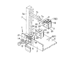
先ず、本実施形態に係る搬送装置及び該搬送装置を備える処理装置の構成例について説明する。図1に、本実施形態に係る搬送装置を用いた処理装置の概略図を示す。また、図2に、本実施形態に係る搬送装置の概略図を示す。
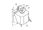
次に、密閉型収納容器20の構造について、図を用いて詳細に説明する。図4に、本実施形態に係る搬送装置7で搬送される密閉型収納装置の概略図を示す。また、図5に、図4の密閉型収容装置の底面の概略図を示す。以後、本明細書における左右とは、図4の水平方向のことを指し、上下(頂面及び底面)とは、図4の鉛直方向のことを指す。
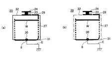
第1の実施形態では、搬送装置7の位置決め用ピン8に接地要素Eを設置することによる、接地の効果を確認した実施形態について説明する。
(1)フランジ24、
(2)支持部27、
(3)その他の部分32(収納容器20の天井面における、フランジ24から蓋体22に対向する側)、
(4)その他の部分32(収納容器20の天井面における、フランジ24から蓋体24側)
の測定箇所で行った(図8の横軸参照)。
第2の実施形態では、搬送装置7の位置決め用ピン8に接地要素Eを設置することによる、ウエハWへのパーティクルの吸着が抑制できることを確認した実施形態について説明する。
2 壁体
3 密閉型収納容器(FOUP)
4 載置台
5 収納棚
6 保持台
7 搬送装置
8 位置決め用ピン
20 収納容器
21 開口部
22 蓋体
23 首部
24 フランジ
25 フランジ部
26 収納容器本体
27 支持部
28 接続部
29 係合溝
30 位置決め溝
40 固定機構
41 固定手段
E 接地要素
S1 ウエハ搬送領域
S2 収納容器搬送領域
W ウエハ
Claims (8)
- 被搬送体を位置決めする第1の位置決め用ピンを有し、前記被搬送体に収納された被処理体を受け渡すための保持台と、
前記被搬送体を前記保持台に載置するために、前記被搬送体を把持するアーム部と、
前記保持台に載置された前記被搬送体を固定するための支持手段と、
を有し、
前記第1の位置決め用ピン、前記アーム部及び前記支持手段の少なくとも1つが、接地要素を有する、
搬送装置。 - 前記第1の位置決め用ピンが接地要素を有し、
前記被搬送体は、前記位置決め用ピンに係合する位置決め溝を有する、
請求項1に記載の搬送装置。 - 前記被搬送体を位置決めする第2の位置決め用ピンを有し、前記被搬送体を搬出入する載置台と、
前記被搬送体を位置決めする第3の位置決め用ピンを有し、前記被搬送体を収納する収納棚と、
を更に有し、
前記第2の位置決め用ピン及び前記第3の位置決め用ピンの少なくとも一方は、接地要素を有する、
請求項1又は2に記載の搬送装置。 - 前記位置決め用ピンは3本のピンであり、
前記3本のピンのいずれか1つが接地要素を有する、
請求項2又は3に記載の搬送装置。 - 前記アーム部が接地要素を有し、
前記被搬送体は、前記アーム部が把時するフランジを有する、
請求項1に記載の搬送装置。 - 前記支持手段が接地要素を有し、
前記保持台は移動可能であり、
前記支持手段は、前記被搬送体の上面の少なくとも一部に係合することによって、移動可能な前記保持台に載置された前記被搬送体を固定する、
請求項1に記載の搬送装置。 - 前記被搬送体は、半導体ウエハを収納した密閉型カセットである、
請求項1乃至6のいずれか一項に記載の搬送装置。 - 請求項1乃至7のいずれか一項に記載の搬送装置と、
前記保持体で受け渡された前記被処理体を熱処理するための熱処理装置と、
を有する、処理装置。
Priority Applications (4)
| Application Number | Priority Date | Filing Date | Title |
|---|---|---|---|
| JP2012209825A JP2014067744A (ja) | 2012-09-24 | 2012-09-24 | 搬送装置及び処理装置 |
| US14/028,640 US20140086712A1 (en) | 2012-09-24 | 2013-09-17 | Transportng apparatus and processing apparatus |
| TW102133851A TW201432839A (zh) | 2012-09-24 | 2013-09-18 | 運送裝置及處理裝置 |
| KR1020130112777A KR20140040652A (ko) | 2012-09-24 | 2013-09-23 | 반송 장치 및 처리 장치 |
Applications Claiming Priority (1)
| Application Number | Priority Date | Filing Date | Title |
|---|---|---|---|
| JP2012209825A JP2014067744A (ja) | 2012-09-24 | 2012-09-24 | 搬送装置及び処理装置 |
Publications (2)
| Publication Number | Publication Date |
|---|---|
| JP2014067744A true JP2014067744A (ja) | 2014-04-17 |
| JP2014067744A5 JP2014067744A5 (ja) | 2015-04-02 |
Family
ID=50339012
Family Applications (1)
| Application Number | Title | Priority Date | Filing Date |
|---|---|---|---|
| JP2012209825A Pending JP2014067744A (ja) | 2012-09-24 | 2012-09-24 | 搬送装置及び処理装置 |
Country Status (4)
| Country | Link |
|---|---|
| US (1) | US20140086712A1 (ja) |
| JP (1) | JP2014067744A (ja) |
| KR (1) | KR20140040652A (ja) |
| TW (1) | TW201432839A (ja) |
Cited By (1)
| Publication number | Priority date | Publication date | Assignee | Title |
|---|---|---|---|---|
| KR20160113013A (ko) | 2015-03-20 | 2016-09-28 | 도쿄엘렉트론가부시키가이샤 | 클램프 장치 및 이것을 이용한 기판 반입출 장치, 및 기판 처리 장치 |
Families Citing this family (6)
| Publication number | Priority date | Publication date | Assignee | Title |
|---|---|---|---|---|
| JP6211938B2 (ja) * | 2014-01-27 | 2017-10-11 | 東京エレクトロン株式会社 | 基板熱処理装置、基板熱処理装置の設置方法 |
| US10807948B2 (en) * | 2015-03-11 | 2020-10-20 | Peloton Therapeutics, Inc. | Aromatic compounds and uses thereof |
| JP6772498B2 (ja) * | 2016-03-18 | 2020-10-21 | 株式会社Sumco | 基板収納容器 |
| JP6693356B2 (ja) * | 2016-09-09 | 2020-05-13 | 株式会社ダイフク | 物品搬送装置 |
| KR102372514B1 (ko) * | 2021-05-10 | 2022-03-10 | 주식회사 위존 | Fims 시스템의 풉 고정장치 |
| KR102372513B1 (ko) * | 2021-05-10 | 2022-03-10 | 주식회사 위존 | Fims 시스템 |
Citations (7)
| Publication number | Priority date | Publication date | Assignee | Title |
|---|---|---|---|---|
| JPH069098U (ja) * | 1992-07-09 | 1994-02-04 | 神鋼電機株式会社 | 搬送装置の帯電静電気放電装置 |
| JP2000100924A (ja) * | 1998-09-18 | 2000-04-07 | Seiko Epson Corp | ウェハカセット及びハンドラー |
| JP2002261159A (ja) * | 2000-12-04 | 2002-09-13 | Ebara Corp | 基板搬送容器 |
| JP2003092328A (ja) * | 2001-09-18 | 2003-03-28 | Dainippon Screen Mfg Co Ltd | ロードポート装置 |
| JP2003282672A (ja) * | 2001-11-08 | 2003-10-03 | Samsung Electronics Co Ltd | 半導体製造設備のカセットテーブル |
| JP2004363363A (ja) * | 2003-06-05 | 2004-12-24 | Tokyo Electron Ltd | 搬送装置及び処理装置並びに搬送方法 |
| JP2005101241A (ja) * | 2003-09-25 | 2005-04-14 | Sumitomo Mitsubishi Silicon Corp | 位置決め部材および容器の支持台 |
Family Cites Families (8)
| Publication number | Priority date | Publication date | Assignee | Title |
|---|---|---|---|---|
| KR100221983B1 (ko) * | 1993-04-13 | 1999-09-15 | 히가시 데쓰로 | 처리장치 |
| US6591162B1 (en) * | 2000-08-15 | 2003-07-08 | Asyst Technologies, Inc. | Smart load port with integrated carrier monitoring and fab-wide carrier management system |
| US6875282B2 (en) * | 2001-05-17 | 2005-04-05 | Ebara Corporation | Substrate transport container |
| WO2004032208A1 (en) * | 2002-10-01 | 2004-04-15 | Microtome Precision, Inc. | Reduction of electric-field-induced damage in field-sensitive articles |
| US7316325B2 (en) * | 2003-11-07 | 2008-01-08 | Entegris, Inc. | Substrate container |
| TWI267483B (en) * | 2004-08-16 | 2006-12-01 | Ind Tech Res Inst | Clean container module |
| US7922485B2 (en) * | 2007-02-14 | 2011-04-12 | Tokyo Electron Limited | Vertical type heat processing apparatus and vertical type heat processing method |
| JP5134495B2 (ja) * | 2008-10-16 | 2013-01-30 | 東京エレクトロン株式会社 | 処理装置及び処理方法 |
-
2012
- 2012-09-24 JP JP2012209825A patent/JP2014067744A/ja active Pending
-
2013
- 2013-09-17 US US14/028,640 patent/US20140086712A1/en not_active Abandoned
- 2013-09-18 TW TW102133851A patent/TW201432839A/zh unknown
- 2013-09-23 KR KR1020130112777A patent/KR20140040652A/ko not_active Application Discontinuation
Patent Citations (7)
| Publication number | Priority date | Publication date | Assignee | Title |
|---|---|---|---|---|
| JPH069098U (ja) * | 1992-07-09 | 1994-02-04 | 神鋼電機株式会社 | 搬送装置の帯電静電気放電装置 |
| JP2000100924A (ja) * | 1998-09-18 | 2000-04-07 | Seiko Epson Corp | ウェハカセット及びハンドラー |
| JP2002261159A (ja) * | 2000-12-04 | 2002-09-13 | Ebara Corp | 基板搬送容器 |
| JP2003092328A (ja) * | 2001-09-18 | 2003-03-28 | Dainippon Screen Mfg Co Ltd | ロードポート装置 |
| JP2003282672A (ja) * | 2001-11-08 | 2003-10-03 | Samsung Electronics Co Ltd | 半導体製造設備のカセットテーブル |
| JP2004363363A (ja) * | 2003-06-05 | 2004-12-24 | Tokyo Electron Ltd | 搬送装置及び処理装置並びに搬送方法 |
| JP2005101241A (ja) * | 2003-09-25 | 2005-04-14 | Sumitomo Mitsubishi Silicon Corp | 位置決め部材および容器の支持台 |
Cited By (4)
| Publication number | Priority date | Publication date | Assignee | Title |
|---|---|---|---|---|
| KR20160113013A (ko) | 2015-03-20 | 2016-09-28 | 도쿄엘렉트론가부시키가이샤 | 클램프 장치 및 이것을 이용한 기판 반입출 장치, 및 기판 처리 장치 |
| JP2016178232A (ja) * | 2015-03-20 | 2016-10-06 | 東京エレクトロン株式会社 | クランプ装置及びこれを用いた基板搬入出装置、並びに基板処理装置 |
| US9857124B2 (en) | 2015-03-20 | 2018-01-02 | Tokyo Electron Limited | Clamp apparatus, substrate carry-in/out apparatus using the same, and substrate processing apparatus |
| TWI651802B (zh) * | 2015-03-20 | 2019-02-21 | 日商東京威力科創股份有限公司 | 夾持裝置及使用此夾持裝置之基板運入運出裝置與基板處理裝置 |
Also Published As
| Publication number | Publication date |
|---|---|
| KR20140040652A (ko) | 2014-04-03 |
| TW201432839A (zh) | 2014-08-16 |
| US20140086712A1 (en) | 2014-03-27 |
Similar Documents
| Publication | Publication Date | Title |
|---|---|---|
| JP2014067744A (ja) | 搬送装置及び処理装置 | |
| JP3880343B2 (ja) | ロードポート、基板処理装置および雰囲気置換方法 | |
| TWI522291B (zh) | Substrate storage container | |
| JP2001516500A (ja) | フラットな対象物を搬送するためのデバイスならびにフラットな対象物を搬送デバイスと処理装置との間にわたって搬送するための方法 | |
| US7347329B2 (en) | Substrate carrier | |
| TWI651802B (zh) | 夾持裝置及使用此夾持裝置之基板運入運出裝置與基板處理裝置 | |
| TWI677051B (zh) | 晶舟支撐台及使用其之熱處理裝置 | |
| JP5001946B2 (ja) | 汚染の影響を受けやすい平坦な物品を保管する、特に、半導体ウェハを保管する装置 | |
| TWI526377B (zh) | 晶圓傳送盒 | |
| JP4927554B2 (ja) | 基板コンテナおよび基板コンテナを製造する方法 | |
| JP2001077188A (ja) | 基板搬送容器 | |
| JP2014067744A5 (ja) | ||
| TW201235276A (en) | Front opening wafer container with robotic flange | |
| JP5867754B2 (ja) | イエロールームシステム | |
| US11387124B2 (en) | Wafer container and method for holding wafer | |
| JP2005353940A (ja) | 半導体基板の保管庫、保管方法及びそれを用いた半導体基板の製造方法 | |
| CN110010535B (zh) | 基板搬入搬出装置、处理装置和基板搬送容器的除电方法 | |
| JP3769425B2 (ja) | 電子部品の製造装置および電子部品の製造方法 | |
| JP6451527B2 (ja) | ミニエンバイロメント装置 | |
| KR102236579B1 (ko) | 오븐 건조 stk 시스템 | |
| JP2015090940A (ja) | ウェーハ搬送装置 | |
| KR20100118290A (ko) | 웨이퍼 이송용 핸들러 | |
| JP2001156144A (ja) | 薄板収納容器開閉装置 | |
| KR20070076208A (ko) | 웨이퍼 수납용 캐리어. | |
| KR20010002584A (ko) | 오염 입자 제거 기능을 갖는 스탠더드 메커니컬 인터페이스 시스템 |
Legal Events
| Date | Code | Title | Description |
|---|---|---|---|
| A521 | Request for written amendment filed |
Free format text: JAPANESE INTERMEDIATE CODE: A523 Effective date: 20150217 |
|
| A621 | Written request for application examination |
Free format text: JAPANESE INTERMEDIATE CODE: A621 Effective date: 20150217 |
|
| A977 | Report on retrieval |
Free format text: JAPANESE INTERMEDIATE CODE: A971007 Effective date: 20150813 |
|
| A131 | Notification of reasons for refusal |
Free format text: JAPANESE INTERMEDIATE CODE: A131 Effective date: 20150818 |
|
| A02 | Decision of refusal |
Free format text: JAPANESE INTERMEDIATE CODE: A02 Effective date: 20160329 |