JP2014036081A - 電子デバイスの製造方法、電子デバイス、電子機器、および移動体 - Google Patents
電子デバイスの製造方法、電子デバイス、電子機器、および移動体 Download PDFInfo
- Publication number
- JP2014036081A JP2014036081A JP2012175752A JP2012175752A JP2014036081A JP 2014036081 A JP2014036081 A JP 2014036081A JP 2012175752 A JP2012175752 A JP 2012175752A JP 2012175752 A JP2012175752 A JP 2012175752A JP 2014036081 A JP2014036081 A JP 2014036081A
- Authority
- JP
- Japan
- Prior art keywords
- lid
- electronic device
- package
- sealing hole
- manufacturing
- Prior art date
- Legal status (The legal status is an assumption and is not a legal conclusion. Google has not performed a legal analysis and makes no representation as to the accuracy of the status listed.)
- Withdrawn
Links
- 238000000034 method Methods 0.000 title claims abstract description 33
- 238000004519 manufacturing process Methods 0.000 title claims abstract description 32
- 238000007789 sealing Methods 0.000 claims abstract description 105
- 238000003466 welding Methods 0.000 claims abstract description 19
- 230000001678 irradiating effect Effects 0.000 claims abstract description 7
- 238000005304 joining Methods 0.000 claims description 26
- 229910052751 metal Inorganic materials 0.000 claims description 22
- 239000002184 metal Substances 0.000 claims description 22
- 239000010931 gold Substances 0.000 claims description 20
- BQCADISMDOOEFD-UHFFFAOYSA-N Silver Chemical compound [Ag] BQCADISMDOOEFD-UHFFFAOYSA-N 0.000 claims description 17
- 229910052709 silver Inorganic materials 0.000 claims description 17
- 239000004332 silver Substances 0.000 claims description 17
- 238000005219 brazing Methods 0.000 claims description 16
- 238000004080 punching Methods 0.000 claims description 13
- PCHJSUWPFVWCPO-UHFFFAOYSA-N gold Chemical compound [Au] PCHJSUWPFVWCPO-UHFFFAOYSA-N 0.000 claims description 10
- 229910052737 gold Inorganic materials 0.000 claims description 10
- ATJFFYVFTNAWJD-UHFFFAOYSA-N Tin Chemical compound [Sn] ATJFFYVFTNAWJD-UHFFFAOYSA-N 0.000 claims description 8
- 229910045601 alloy Inorganic materials 0.000 claims description 8
- 239000000956 alloy Substances 0.000 claims description 8
- 238000002360 preparation method Methods 0.000 claims description 5
- 229910000679 solder Inorganic materials 0.000 claims description 4
- 239000013078 crystal Substances 0.000 abstract description 24
- PXHVJJICTQNCMI-UHFFFAOYSA-N Nickel Chemical compound [Ni] PXHVJJICTQNCMI-UHFFFAOYSA-N 0.000 description 18
- 230000002093 peripheral effect Effects 0.000 description 16
- 239000000463 material Substances 0.000 description 10
- 239000012298 atmosphere Substances 0.000 description 9
- 230000008018 melting Effects 0.000 description 7
- 238000002844 melting Methods 0.000 description 7
- 239000010453 quartz Substances 0.000 description 7
- VYPSYNLAJGMNEJ-UHFFFAOYSA-N silicon dioxide Inorganic materials O=[Si]=O VYPSYNLAJGMNEJ-UHFFFAOYSA-N 0.000 description 7
- 229910052759 nickel Inorganic materials 0.000 description 6
- 238000007747 plating Methods 0.000 description 6
- 239000000853 adhesive Substances 0.000 description 5
- 230000001070 adhesive effect Effects 0.000 description 5
- 238000010438 heat treatment Methods 0.000 description 5
- 229910000833 kovar Inorganic materials 0.000 description 5
- 230000000694 effects Effects 0.000 description 4
- 230000005284 excitation Effects 0.000 description 4
- 239000004593 Epoxy Substances 0.000 description 2
- KRHYYFGTRYWZRS-UHFFFAOYSA-N Fluorane Chemical compound F KRHYYFGTRYWZRS-UHFFFAOYSA-N 0.000 description 2
- 230000001133 acceleration Effects 0.000 description 2
- 239000003795 chemical substances by application Substances 0.000 description 2
- 239000011651 chromium Substances 0.000 description 2
- 230000007797 corrosion Effects 0.000 description 2
- 238000005260 corrosion Methods 0.000 description 2
- 238000007872 degassing Methods 0.000 description 2
- 238000000605 extraction Methods 0.000 description 2
- 239000010419 fine particle Substances 0.000 description 2
- 229910052451 lead zirconate titanate Inorganic materials 0.000 description 2
- 238000001465 metallisation Methods 0.000 description 2
- 238000012545 processing Methods 0.000 description 2
- 230000035939 shock Effects 0.000 description 2
- 229920003002 synthetic resin Polymers 0.000 description 2
- 239000000057 synthetic resin Substances 0.000 description 2
- 238000007740 vapor deposition Methods 0.000 description 2
- WSMQKESQZFQMFW-UHFFFAOYSA-N 5-methyl-pyrazole-3-carboxylic acid Chemical compound CC1=CC(C(O)=O)=NN1 WSMQKESQZFQMFW-UHFFFAOYSA-N 0.000 description 1
- 241000251468 Actinopterygii Species 0.000 description 1
- PIGFYZPCRLYGLF-UHFFFAOYSA-N Aluminum nitride Chemical compound [Al]#N PIGFYZPCRLYGLF-UHFFFAOYSA-N 0.000 description 1
- VYZAMTAEIAYCRO-UHFFFAOYSA-N Chromium Chemical compound [Cr] VYZAMTAEIAYCRO-UHFFFAOYSA-N 0.000 description 1
- 229910000640 Fe alloy Inorganic materials 0.000 description 1
- WQZGKKKJIJFFOK-GASJEMHNSA-N Glucose Natural products OC[C@H]1OC(O)[C@H](O)[C@@H](O)[C@@H]1O WQZGKKKJIJFFOK-GASJEMHNSA-N 0.000 description 1
- XEEYBQQBJWHFJM-UHFFFAOYSA-N Iron Chemical compound [Fe] XEEYBQQBJWHFJM-UHFFFAOYSA-N 0.000 description 1
- 229910013641 LiNbO 3 Inorganic materials 0.000 description 1
- 239000004642 Polyimide Substances 0.000 description 1
- XLOMVQKBTHCTTD-UHFFFAOYSA-N Zinc monoxide Chemical compound [Zn]=O XLOMVQKBTHCTTD-UHFFFAOYSA-N 0.000 description 1
- 239000008280 blood Substances 0.000 description 1
- 210000004369 blood Anatomy 0.000 description 1
- 230000036772 blood pressure Effects 0.000 description 1
- 229910010293 ceramic material Inorganic materials 0.000 description 1
- 229910052804 chromium Inorganic materials 0.000 description 1
- 229910017052 cobalt Inorganic materials 0.000 description 1
- 239000010941 cobalt Substances 0.000 description 1
- GUTLYIVDDKVIGB-UHFFFAOYSA-N cobalt atom Chemical compound [Co] GUTLYIVDDKVIGB-UHFFFAOYSA-N 0.000 description 1
- 238000004891 communication Methods 0.000 description 1
- 238000012790 confirmation Methods 0.000 description 1
- 238000007796 conventional method Methods 0.000 description 1
- 230000006837 decompression Effects 0.000 description 1
- 238000000151 deposition Methods 0.000 description 1
- PSHMSSXLYVAENJ-UHFFFAOYSA-N dilithium;[oxido(oxoboranyloxy)boranyl]oxy-oxoboranyloxyborinate Chemical compound [Li+].[Li+].O=BOB([O-])OB([O-])OB=O PSHMSSXLYVAENJ-UHFFFAOYSA-N 0.000 description 1
- 238000005553 drilling Methods 0.000 description 1
- 238000010894 electron beam technology Methods 0.000 description 1
- 229910052732 germanium Inorganic materials 0.000 description 1
- GNPVGFCGXDBREM-UHFFFAOYSA-N germanium atom Chemical compound [Ge] GNPVGFCGXDBREM-UHFFFAOYSA-N 0.000 description 1
- 239000008103 glucose Substances 0.000 description 1
- 239000011261 inert gas Substances 0.000 description 1
- 239000011810 insulating material Substances 0.000 description 1
- HFGPZNIAWCZYJU-UHFFFAOYSA-N lead zirconate titanate Chemical compound [O-2].[O-2].[O-2].[O-2].[O-2].[Ti+4].[Zr+4].[Pb+2] HFGPZNIAWCZYJU-UHFFFAOYSA-N 0.000 description 1
- GQYHUHYESMUTHG-UHFFFAOYSA-N lithium niobate Chemical compound [Li+].[O-][Nb](=O)=O GQYHUHYESMUTHG-UHFFFAOYSA-N 0.000 description 1
- 229910052574 oxide ceramic Inorganic materials 0.000 description 1
- 239000011224 oxide ceramic Substances 0.000 description 1
- TWNQGVIAIRXVLR-UHFFFAOYSA-N oxo(oxoalumanyloxy)alumane Chemical compound O=[Al]O[Al]=O TWNQGVIAIRXVLR-UHFFFAOYSA-N 0.000 description 1
- 238000000206 photolithography Methods 0.000 description 1
- 229920001721 polyimide Polymers 0.000 description 1
- 229920001296 polysiloxane Polymers 0.000 description 1
- 230000002265 prevention Effects 0.000 description 1
- 229920005989 resin Polymers 0.000 description 1
- 239000011347 resin Substances 0.000 description 1
- 238000007665 sagging Methods 0.000 description 1
- 229910052710 silicon Inorganic materials 0.000 description 1
- 239000010703 silicon Substances 0.000 description 1
- 238000005245 sintering Methods 0.000 description 1
- 238000004544 sputter deposition Methods 0.000 description 1
- 230000006641 stabilisation Effects 0.000 description 1
- 238000011105 stabilization Methods 0.000 description 1
- 239000010935 stainless steel Substances 0.000 description 1
- 229910001220 stainless steel Inorganic materials 0.000 description 1
- 239000000758 substrate Substances 0.000 description 1
- 238000001039 wet etching Methods 0.000 description 1
Images


Classifications
-
- H—ELECTRICITY
- H05—ELECTRIC TECHNIQUES NOT OTHERWISE PROVIDED FOR
- H05K—PRINTED CIRCUITS; CASINGS OR CONSTRUCTIONAL DETAILS OF ELECTRIC APPARATUS; MANUFACTURE OF ASSEMBLAGES OF ELECTRICAL COMPONENTS
- H05K3/00—Apparatus or processes for manufacturing printed circuits
- H05K3/30—Assembling printed circuits with electric components, e.g. with resistor
-
- H—ELECTRICITY
- H01—ELECTRIC ELEMENTS
- H01L—SEMICONDUCTOR DEVICES NOT COVERED BY CLASS H10
- H01L23/00—Details of semiconductor or other solid state devices
- H01L23/02—Containers; Seals
- H01L23/10—Containers; Seals characterised by the material or arrangement of seals between parts, e.g. between cap and base of the container or between leads and walls of the container
-
- H—ELECTRICITY
- H01—ELECTRIC ELEMENTS
- H01L—SEMICONDUCTOR DEVICES NOT COVERED BY CLASS H10
- H01L21/00—Processes or apparatus adapted for the manufacture or treatment of semiconductor or solid state devices or of parts thereof
- H01L21/02—Manufacture or treatment of semiconductor devices or of parts thereof
- H01L21/04—Manufacture or treatment of semiconductor devices or of parts thereof the devices having potential barriers, e.g. a PN junction, depletion layer or carrier concentration layer
- H01L21/50—Assembly of semiconductor devices using processes or apparatus not provided for in a single one of the subgroups H01L21/06 - H01L21/326, e.g. sealing of a cap to a base of a container
- H01L21/54—Providing fillings in containers, e.g. gas fillings
-
- H—ELECTRICITY
- H05—ELECTRIC TECHNIQUES NOT OTHERWISE PROVIDED FOR
- H05K—PRINTED CIRCUITS; CASINGS OR CONSTRUCTIONAL DETAILS OF ELECTRIC APPARATUS; MANUFACTURE OF ASSEMBLAGES OF ELECTRICAL COMPONENTS
- H05K7/00—Constructional details common to different types of electric apparatus
- H05K7/02—Arrangements of circuit components or wiring on supporting structure
-
- H—ELECTRICITY
- H01—ELECTRIC ELEMENTS
- H01L—SEMICONDUCTOR DEVICES NOT COVERED BY CLASS H10
- H01L2924/00—Indexing scheme for arrangements or methods for connecting or disconnecting semiconductor or solid-state bodies as covered by H01L24/00
- H01L2924/0001—Technical content checked by a classifier
- H01L2924/0002—Not covered by any one of groups H01L24/00, H01L24/00 and H01L2224/00
-
- H—ELECTRICITY
- H03—ELECTRONIC CIRCUITRY
- H03H—IMPEDANCE NETWORKS, e.g. RESONANT CIRCUITS; RESONATORS
- H03H3/00—Apparatus or processes specially adapted for the manufacture of impedance networks, resonating circuits, resonators
- H03H3/007—Apparatus or processes specially adapted for the manufacture of impedance networks, resonating circuits, resonators for the manufacture of electromechanical resonators or networks
- H03H3/0072—Apparatus or processes specially adapted for the manufacture of impedance networks, resonating circuits, resonators for the manufacture of electromechanical resonators or networks of microelectro-mechanical resonators or networks
-
- H—ELECTRICITY
- H03—ELECTRONIC CIRCUITRY
- H03H—IMPEDANCE NETWORKS, e.g. RESONANT CIRCUITS; RESONATORS
- H03H3/00—Apparatus or processes specially adapted for the manufacture of impedance networks, resonating circuits, resonators
- H03H3/007—Apparatus or processes specially adapted for the manufacture of impedance networks, resonating circuits, resonators for the manufacture of electromechanical resonators or networks
- H03H3/02—Apparatus or processes specially adapted for the manufacture of impedance networks, resonating circuits, resonators for the manufacture of electromechanical resonators or networks for the manufacture of piezoelectric or electrostrictive resonators or networks
-
- H—ELECTRICITY
- H03—ELECTRONIC CIRCUITRY
- H03H—IMPEDANCE NETWORKS, e.g. RESONANT CIRCUITS; RESONATORS
- H03H9/00—Networks comprising electromechanical or electro-acoustic devices; Electromechanical resonators
- H03H9/02—Details
- H03H9/05—Holders; Supports
- H03H9/10—Mounting in enclosures
-
- Y—GENERAL TAGGING OF NEW TECHNOLOGICAL DEVELOPMENTS; GENERAL TAGGING OF CROSS-SECTIONAL TECHNOLOGIES SPANNING OVER SEVERAL SECTIONS OF THE IPC; TECHNICAL SUBJECTS COVERED BY FORMER USPC CROSS-REFERENCE ART COLLECTIONS [XRACs] AND DIGESTS
- Y10—TECHNICAL SUBJECTS COVERED BY FORMER USPC
- Y10T—TECHNICAL SUBJECTS COVERED BY FORMER US CLASSIFICATION
- Y10T29/00—Metal working
- Y10T29/49—Method of mechanical manufacture
- Y10T29/49002—Electrical device making
- Y10T29/49117—Conductor or circuit manufacturing
- Y10T29/49124—On flat or curved insulated base, e.g., printed circuit, etc.
- Y10T29/4913—Assembling to base an electrical component, e.g., capacitor, etc.
- Y10T29/49144—Assembling to base an electrical component, e.g., capacitor, etc. by metal fusion
Landscapes
- Engineering & Computer Science (AREA)
- Microelectronics & Electronic Packaging (AREA)
- Physics & Mathematics (AREA)
- Condensed Matter Physics & Semiconductors (AREA)
- General Physics & Mathematics (AREA)
- Computer Hardware Design (AREA)
- Power Engineering (AREA)
- Manufacturing & Machinery (AREA)
- Piezo-Electric Or Mechanical Vibrators, Or Delay Or Filter Circuits (AREA)
Abstract
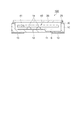
【解決手段】電子デバイス100の製造方法は、封止孔25aを有する蓋体20と、シームリング(メタライズ部)30を有し蓋体20と共に内部空間Sを構成するためのパッケージ10と、水晶振動片(電子部品)40とを用意する準備工程と、水晶振動片40をパッケージ10に搭載する搭載工程と、封止孔25aとシームリング30とが平面視で重なるように蓋体20をパッケージ10に載置する載置工程と、蓋体20の外周部とパッケージ10とをシーム溶接する第1接合工程と、エネルギービームBを照射して封止孔25aとシームリング30とを接合し封止孔25aと内部空間Sとを封止する第2接合工程と、
を含むことを特徴とする。
【選択図】図4
Description
(実施形態1)
(実施形態2)
(実施形態3)
(電子機器)
Claims (9)
- 封止孔を有する蓋体と、メタライズ部を有し前記蓋体と共に内部空間を構成するためのパッケージと、電子部品とを用意する準備工程と、
前記電子部品を前記パッケージに搭載する搭載工程と、
前記封止孔と前記メタライズ部とが平面視で重なるように前記蓋体を前記パッケージに載置する載置工程と、
前記蓋体の外周部と前記パッケージとをシーム溶接する第1接合工程と、
エネルギービームを照射して前記封止孔と前記メタライズ部とを接合し前記封止孔と前記内部空間とを封止する第2接合工程と、
を含むことを特徴とする電子デバイスの製造方法。 - 前記蓋体の一方の面には金属ロウが配置され、
前記第2接合工程では、前記蓋体の前記メタライズ部に載置される面側に前記一方の面を配置し、前記封止孔と前記メタライズ部とを前記金属ロウによって接合する、ことを特徴とする請求項1に記載の電子デバイスの製造方法。 - 前記金属ロウが、銀ロウまたは金(Au)/錫(Sn)合金ロウである、ことを特徴とする請求項2に記載の電子デバイスの製造方法。
- 前記第2接合工程では、前記封止孔の内面と前記メタライズ部との間にフィレット状部を形成する、ことを特徴とする請求項1から3のいずれか一項に記載の電子デバイスの製造方法。
- 前記準備工程で用意する前記パッケージの前記メタライズ部は、前記封止孔が配置される位置を通る平面視幅が他の位置における平面視幅より大きい、ことを特徴とする請求項1から4のいずれか一項に記載の電子デバイスの製造方法。
- 前記封止孔はプレス抜き加工で形成されており、
前記載置工程では、前記蓋体の抜き加工開始側の面が前記パッケージに載置される、ことを特徴とする請求項1から5のいずれか一項に記載の電子デバイスの製造方法。 - 孔部を有している蓋体、パッケージ、および前記蓋体と前記パッケージとが接合して構成されている内部空間にある電子部品とを備え、前記孔部は前記蓋体と前記パッケージとの接合部と平面視で重なる位置に配置されていること、を特徴とする電子デバイス。
- 請求項1から6のいずれか一項に記載の製造方法によって製造された電子デバイスを搭載している、ことを特徴とする電子機器。
- 請求項1から6のいずれか一項に記載の製造方法によって製造された電子デバイスを搭載している、ことを特徴とする移動体。
Priority Applications (3)
| Application Number | Priority Date | Filing Date | Title |
|---|---|---|---|
| JP2012175752A JP2014036081A (ja) | 2012-08-08 | 2012-08-08 | 電子デバイスの製造方法、電子デバイス、電子機器、および移動体 |
| CN201310336702.2A CN103579014A (zh) | 2012-08-08 | 2013-08-05 | 电子器件的制造方法、电子器件、电子设备以及移动体 |
| US13/959,877 US20140043779A1 (en) | 2012-08-08 | 2013-08-06 | Method of manufacturing electronic device, electronic device, electronic apparatus, and mobile object |
Applications Claiming Priority (1)
| Application Number | Priority Date | Filing Date | Title |
|---|---|---|---|
| JP2012175752A JP2014036081A (ja) | 2012-08-08 | 2012-08-08 | 電子デバイスの製造方法、電子デバイス、電子機器、および移動体 |
Publications (2)
| Publication Number | Publication Date |
|---|---|
| JP2014036081A true JP2014036081A (ja) | 2014-02-24 |
| JP2014036081A5 JP2014036081A5 (ja) | 2015-09-10 |
Family
ID=50050520
Family Applications (1)
| Application Number | Title | Priority Date | Filing Date |
|---|---|---|---|
| JP2012175752A Withdrawn JP2014036081A (ja) | 2012-08-08 | 2012-08-08 | 電子デバイスの製造方法、電子デバイス、電子機器、および移動体 |
Country Status (3)
| Country | Link |
|---|---|
| US (1) | US20140043779A1 (ja) |
| JP (1) | JP2014036081A (ja) |
| CN (1) | CN103579014A (ja) |
Cited By (1)
| Publication number | Priority date | Publication date | Assignee | Title |
|---|---|---|---|---|
| WO2019059338A1 (ja) * | 2017-09-22 | 2019-03-28 | 株式会社村田製作所 | 圧電振動子及び圧電振動子の製造方法 |
Families Citing this family (3)
| Publication number | Priority date | Publication date | Assignee | Title |
|---|---|---|---|---|
| JP6167494B2 (ja) * | 2012-09-26 | 2017-07-26 | セイコーエプソン株式会社 | 電子デバイス用容器の製造方法、電子デバイスの製造方法、電子デバイス、電子機器及び移動体機器 |
| CN106028649B (zh) * | 2016-07-28 | 2019-02-12 | Oppo广东移动通信有限公司 | 移动终端的电路板和具有其的移动终端 |
| DE102017125140B4 (de) * | 2017-10-26 | 2021-06-10 | Infineon Technologies Ag | Verfahren zum Herstellen eines hermetisch abgedichteten Gehäuses mit einem Halbleiterbauteil |
Citations (7)
| Publication number | Priority date | Publication date | Assignee | Title |
|---|---|---|---|---|
| JPS5232269A (en) * | 1975-09-05 | 1977-03-11 | Matsushita Electric Ind Co Ltd | Hermetic sealing method of semiconductor devices |
| JPH10189795A (ja) * | 1996-12-19 | 1998-07-21 | Murata Mfg Co Ltd | 素子のパッケージ構造およびその製造方法 |
| JP2004266239A (ja) * | 2003-01-10 | 2004-09-24 | Seiko Epson Corp | 圧電デバイス |
| JP2004289238A (ja) * | 2003-03-19 | 2004-10-14 | Seiko Epson Corp | 圧電デバイス用パッケージと圧電デバイスおよびこれらの製造方法ならびに圧電デバイスを利用した携帯電話装置および圧電デバイスを利用した電子機器 |
| JP2004320150A (ja) * | 2003-04-11 | 2004-11-11 | Seiko Epson Corp | 圧電デバイス、圧電デバイス用パッケージ、および圧電デバイスの製造方法 |
| WO2010010721A1 (ja) * | 2008-07-25 | 2010-01-28 | 日本電気株式会社 | 封止パッケージ、プリント回路基板、電子機器及び封止パッケージの製造方法 |
| JP2010119141A (ja) * | 2010-02-22 | 2010-05-27 | Kyocera Corp | デバイス装置 |
Family Cites Families (3)
| Publication number | Priority date | Publication date | Assignee | Title |
|---|---|---|---|---|
| US5041695A (en) * | 1989-06-01 | 1991-08-20 | Westinghouse Electric Corp. | Co-fired ceramic package for a power circuit |
| US20040241906A1 (en) * | 2003-05-28 | 2004-12-02 | Vincent Chan | Integrated circuit package and method for making same that employs under bump metalization layer |
| JP5007494B2 (ja) * | 2005-07-04 | 2012-08-22 | セイコーエプソン株式会社 | 電子デバイスの製造方法 |
-
2012
- 2012-08-08 JP JP2012175752A patent/JP2014036081A/ja not_active Withdrawn
-
2013
- 2013-08-05 CN CN201310336702.2A patent/CN103579014A/zh active Pending
- 2013-08-06 US US13/959,877 patent/US20140043779A1/en not_active Abandoned
Patent Citations (7)
| Publication number | Priority date | Publication date | Assignee | Title |
|---|---|---|---|---|
| JPS5232269A (en) * | 1975-09-05 | 1977-03-11 | Matsushita Electric Ind Co Ltd | Hermetic sealing method of semiconductor devices |
| JPH10189795A (ja) * | 1996-12-19 | 1998-07-21 | Murata Mfg Co Ltd | 素子のパッケージ構造およびその製造方法 |
| JP2004266239A (ja) * | 2003-01-10 | 2004-09-24 | Seiko Epson Corp | 圧電デバイス |
| JP2004289238A (ja) * | 2003-03-19 | 2004-10-14 | Seiko Epson Corp | 圧電デバイス用パッケージと圧電デバイスおよびこれらの製造方法ならびに圧電デバイスを利用した携帯電話装置および圧電デバイスを利用した電子機器 |
| JP2004320150A (ja) * | 2003-04-11 | 2004-11-11 | Seiko Epson Corp | 圧電デバイス、圧電デバイス用パッケージ、および圧電デバイスの製造方法 |
| WO2010010721A1 (ja) * | 2008-07-25 | 2010-01-28 | 日本電気株式会社 | 封止パッケージ、プリント回路基板、電子機器及び封止パッケージの製造方法 |
| JP2010119141A (ja) * | 2010-02-22 | 2010-05-27 | Kyocera Corp | デバイス装置 |
Cited By (3)
| Publication number | Priority date | Publication date | Assignee | Title |
|---|---|---|---|---|
| WO2019059338A1 (ja) * | 2017-09-22 | 2019-03-28 | 株式会社村田製作所 | 圧電振動子及び圧電振動子の製造方法 |
| JPWO2019059338A1 (ja) * | 2017-09-22 | 2020-11-12 | 株式会社村田製作所 | 圧電振動子及び圧電振動子の製造方法 |
| US11309864B2 (en) | 2017-09-22 | 2022-04-19 | Murata Manufacturing Co., Ltd. | Piezoelectric resonator unit and method for manufacturing the piezoelectric resonator unit |
Also Published As
| Publication number | Publication date |
|---|---|
| CN103579014A (zh) | 2014-02-12 |
| US20140043779A1 (en) | 2014-02-13 |
Similar Documents
| Publication | Publication Date | Title |
|---|---|---|
| JP6167494B2 (ja) | 電子デバイス用容器の製造方法、電子デバイスの製造方法、電子デバイス、電子機器及び移動体機器 | |
| JP4462332B2 (ja) | 電子部品 | |
| JP2008218811A (ja) | 機能素子パッケージ | |
| US9509276B2 (en) | Acoustic wave device and method of fabricating the same | |
| WO2008018222A1 (fr) | Dispositif piézoélectrique de vibrations | |
| JP2014036081A (ja) | 電子デバイスの製造方法、電子デバイス、電子機器、および移動体 | |
| JP2007059736A (ja) | 圧電振動子パッケージ及びその製造方法ならびに物理量センサ | |
| JP2013046167A (ja) | 振動デバイス、及び振動デバイスの製造方法 | |
| JP2005143042A (ja) | 圧電デバイス | |
| JP2014197575A (ja) | パッケージ、電子デバイス、電子デバイスの製造方法、電子機器、及び移動体 | |
| JP5505189B2 (ja) | 振動デバイスおよび電子機器 | |
| JP2007251239A (ja) | 圧電デバイスおよび圧電デバイスの製造方法 | |
| JP5251224B2 (ja) | 圧電振動デバイスの製造方法および圧電振動デバイス | |
| JP2015094614A (ja) | 蓋体、パッケージ、電子機器、移動体、およびパッケージの製造方法 | |
| JP2006086585A (ja) | 表面実装型圧電振動デバイス | |
| JP2007073713A (ja) | 圧電デバイス用パッケージ | |
| JP3922570B2 (ja) | 圧電デバイスと圧電デバイス用パッケージ、圧電デバイスの製造方法、ならびに圧電デバイスを利用した携帯電話装置ならびに圧電デバイスを利用した電子機器 | |
| JP5196121B2 (ja) | デバイス | |
| JP2014110370A (ja) | ベース基板、実装構造体、モジュール、電子機器、および移動体 | |
| JP2003069368A (ja) | 圧電デバイスと圧電振動片の接合方法、及び圧電デバイスを利用した携帯電話装置ならびに圧電デバイスを利用した電子機器 | |
| JP2017212612A (ja) | 圧電デバイス及びその製造方法 | |
| JP2001274649A (ja) | 水晶振動デバイスの気密封止方法 | |
| JP2009117869A (ja) | 機能素子パッケージの製造方法 | |
| JP2007318209A (ja) | 表面実装型圧電振動デバイス、およびその製造方法 | |
| JP4599145B2 (ja) | 圧電振動板 |
Legal Events
| Date | Code | Title | Description |
|---|---|---|---|
| RD04 | Notification of resignation of power of attorney |
Free format text: JAPANESE INTERMEDIATE CODE: A7424 Effective date: 20150108 |
|
| A521 | Request for written amendment filed |
Free format text: JAPANESE INTERMEDIATE CODE: A523 Effective date: 20150722 |
|
| A621 | Written request for application examination |
Free format text: JAPANESE INTERMEDIATE CODE: A621 Effective date: 20150722 |
|
| RD04 | Notification of resignation of power of attorney |
Free format text: JAPANESE INTERMEDIATE CODE: A7424 Effective date: 20160610 |
|
| RD03 | Notification of appointment of power of attorney |
Free format text: JAPANESE INTERMEDIATE CODE: A7423 Effective date: 20160624 |
|
| A977 | Report on retrieval |
Free format text: JAPANESE INTERMEDIATE CODE: A971007 Effective date: 20160725 |
|
| A131 | Notification of reasons for refusal |
Free format text: JAPANESE INTERMEDIATE CODE: A131 Effective date: 20160802 |
|
| A761 | Written withdrawal of application |
Free format text: JAPANESE INTERMEDIATE CODE: A761 Effective date: 20160923 |