JP2013246320A - 半導体光素子、及び光モジュール - Google Patents
半導体光素子、及び光モジュール Download PDFInfo
- Publication number
- JP2013246320A JP2013246320A JP2012120078A JP2012120078A JP2013246320A JP 2013246320 A JP2013246320 A JP 2013246320A JP 2012120078 A JP2012120078 A JP 2012120078A JP 2012120078 A JP2012120078 A JP 2012120078A JP 2013246320 A JP2013246320 A JP 2013246320A
- Authority
- JP
- Japan
- Prior art keywords
- substrate
- semiconductor optical
- optical device
- conductive film
- pyroelectric
- Prior art date
- Legal status (The legal status is an assumption and is not a legal conclusion. Google has not performed a legal analysis and makes no representation as to the accuracy of the status listed.)
- Pending
Links
Images


Classifications
-
- G—PHYSICS
- G02—OPTICS
- G02B—OPTICAL ELEMENTS, SYSTEMS OR APPARATUS
- G02B6/00—Light guides; Structural details of arrangements comprising light guides and other optical elements, e.g. couplings
- G02B6/10—Light guides; Structural details of arrangements comprising light guides and other optical elements, e.g. couplings of the optical waveguide type
- G02B6/12—Light guides; Structural details of arrangements comprising light guides and other optical elements, e.g. couplings of the optical waveguide type of the integrated circuit kind
- G02B6/12004—Combinations of two or more optical elements
-
- G—PHYSICS
- G02—OPTICS
- G02F—OPTICAL DEVICES OR ARRANGEMENTS FOR THE CONTROL OF LIGHT BY MODIFICATION OF THE OPTICAL PROPERTIES OF THE MEDIA OF THE ELEMENTS INVOLVED THEREIN; NON-LINEAR OPTICS; FREQUENCY-CHANGING OF LIGHT; OPTICAL LOGIC ELEMENTS; OPTICAL ANALOGUE/DIGITAL CONVERTERS
- G02F1/00—Devices or arrangements for the control of the intensity, colour, phase, polarisation or direction of light arriving from an independent light source, e.g. switching, gating or modulating; Non-linear optics
- G02F1/01—Devices or arrangements for the control of the intensity, colour, phase, polarisation or direction of light arriving from an independent light source, e.g. switching, gating or modulating; Non-linear optics for the control of the intensity, phase, polarisation or colour
- G02F1/03—Devices or arrangements for the control of the intensity, colour, phase, polarisation or direction of light arriving from an independent light source, e.g. switching, gating or modulating; Non-linear optics for the control of the intensity, phase, polarisation or colour based on ceramics or electro-optical crystals, e.g. exhibiting Pockels effect or Kerr effect
- G02F1/035—Devices or arrangements for the control of the intensity, colour, phase, polarisation or direction of light arriving from an independent light source, e.g. switching, gating or modulating; Non-linear optics for the control of the intensity, phase, polarisation or colour based on ceramics or electro-optical crystals, e.g. exhibiting Pockels effect or Kerr effect in an optical waveguide structure
-
- G—PHYSICS
- G02—OPTICS
- G02F—OPTICAL DEVICES OR ARRANGEMENTS FOR THE CONTROL OF LIGHT BY MODIFICATION OF THE OPTICAL PROPERTIES OF THE MEDIA OF THE ELEMENTS INVOLVED THEREIN; NON-LINEAR OPTICS; FREQUENCY-CHANGING OF LIGHT; OPTICAL LOGIC ELEMENTS; OPTICAL ANALOGUE/DIGITAL CONVERTERS
- G02F1/00—Devices or arrangements for the control of the intensity, colour, phase, polarisation or direction of light arriving from an independent light source, e.g. switching, gating or modulating; Non-linear optics
- G02F1/01—Devices or arrangements for the control of the intensity, colour, phase, polarisation or direction of light arriving from an independent light source, e.g. switching, gating or modulating; Non-linear optics for the control of the intensity, phase, polarisation or colour
- G02F1/21—Devices or arrangements for the control of the intensity, colour, phase, polarisation or direction of light arriving from an independent light source, e.g. switching, gating or modulating; Non-linear optics for the control of the intensity, phase, polarisation or colour by interference
- G02F1/225—Devices or arrangements for the control of the intensity, colour, phase, polarisation or direction of light arriving from an independent light source, e.g. switching, gating or modulating; Non-linear optics for the control of the intensity, phase, polarisation or colour by interference in an optical waveguide structure
-
- G—PHYSICS
- G02—OPTICS
- G02F—OPTICAL DEVICES OR ARRANGEMENTS FOR THE CONTROL OF LIGHT BY MODIFICATION OF THE OPTICAL PROPERTIES OF THE MEDIA OF THE ELEMENTS INVOLVED THEREIN; NON-LINEAR OPTICS; FREQUENCY-CHANGING OF LIGHT; OPTICAL LOGIC ELEMENTS; OPTICAL ANALOGUE/DIGITAL CONVERTERS
- G02F2201/00—Constructional arrangements not provided for in groups G02F1/00 - G02F7/00
- G02F2201/50—Protective arrangements
Landscapes
- Physics & Mathematics (AREA)
- Nonlinear Science (AREA)
- General Physics & Mathematics (AREA)
- Optics & Photonics (AREA)
- Engineering & Computer Science (AREA)
- Microelectronics & Electronic Packaging (AREA)
- Chemical & Material Sciences (AREA)
- Ceramic Engineering (AREA)
- Crystallography & Structural Chemistry (AREA)
- Optical Modulation, Optical Deflection, Nonlinear Optics, Optical Demodulation, Optical Logic Elements (AREA)
Abstract
【解決手段】本発明に係る半導体光素子は、上表面に光導波路が形成され、電気光学効果を有するとともに焦電性である、第1の基板と、前記第1の基板の下表面と、絶縁性の接着層を介して、上表面が接続される、第2の基板と、を備える半導体光素子であって、前記第1の基板の前記下表面に第1の導電性膜が形成され、前記第1の基板の少なくとも一の側面及び該側面に対応する前記第2の基板の側面に、第2の導電性膜が形成され、前記第1の導電性膜は、前記第2の導電性膜と、電気的に接続される、ことを特徴とする。
【選択図】図2
Description
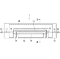
図1は、本発明の第1の実施形態に係る半導体光素子1の概略上面図である。当該実施形態に係る半導体光素子1は、導波路型MZ変調素子(LN変調器)である。半導体光素子1は、変調基板10(第1の基板)を備え、変調基板10の上表面に光導波路が形成されている。変調基板10には、電気光学結晶が用いられており、変調基板10は、電気光学効果を有するとともに焦電性である。長距離高速光ファイバ通信を実現するために、電気のデータ信号を光信号を変調するための光変調器が必要であり、当該実施形態に係る半導体光素子は、長距離伝送用に用いる光変調器に最適である。
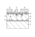
図5は、本発明の第2の実施形態に係る半導体光素子1の焦電効果を示す概略断面図である。当該実施形態に係る半導体光素子1は、補強基板31の構成が異なることを除いて、第1の実施形態に係る半導体光素子1と同じ構造をしている。
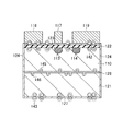
本発明の第3の実施形態に係る光モジュールは、第1又は第2の実施形態に係る半導体光素子1と、導電性のパッケージとを備える光モジュール(図示せず)である。半導体光素子1は、導電性の接着材によりパッケージに固定して搭載される。第1の実施形態に係る半導体光素子1では、補強基板21の下表面に導電性膜27が形成されており、また、第2の実施形態に係る半導体光素子1では、補強基板31が高い電気伝導性を有していることにより、半導体光素子1に形成される導電性膜は、パッケージと電気的に接続されている。よって、変調基板10の下表面に形成される導電性膜25に、外部よりパッケージを介して、より安定的に電荷が供給され、本発明の効果はさらに高まる。
Claims (11)
- 上表面に光導波路が形成され、電気光学効果を有するとともに焦電性である、第1の基板と、
前記第1の基板の下表面と、絶縁性の接着層を介して、上表面が接続される、第2の基板と、
を備える半導体光素子であって、
前記第1の基板の前記下表面に第1の導電性膜が形成され、
前記第1の基板の少なくとも一の側面及び該側面に対応する前記第2の基板の側面に、第2の導電性膜が形成され、
前記第1の導電性膜は、前記第2の導電性膜と、電気的に接続される、
ことを特徴とする、半導体光素子。 - 請求項1に記載の半導体光素子であって、
前記第2の基板は、前記第1の基板と熱膨張係数が略等しい、
ことを特徴とする、半導体光素子。 - 請求項1又は2に記載の半導体光素子であって、
前記第2の基板の前記上表面に第3の導電性膜が形成され、
前記第3の導電性膜は、前記第2の導電性膜と、電気的に接続される、
ことを特徴とする、半導体光素子。 - 請求項1又は2に記載の半導体光素子であって、
前記第2の基板は、前記第1の基板より、電気伝導性が高い、
ことを特徴とする、半導体光素子。 - 請求項3に記載の半導体光素子であって、
前記第1の基板の材料及び前記第2の基板の材料は、ともに、ニオブ酸リチウム、タンタル酸リチウム、又はニオブ酸タンタル酸リチウムのいずれかである、
ことを特徴とする、半導体光素子。 - 請求項4に記載の半導体光素子であって、
前記第1の基板の材料は、ニオブ酸リチウム、タンタル酸リチウム、又はニオブ酸タンタル酸リチウムのいずれかであり、
前記第2の基板の材料は、ブラックニオブ酸リチウム、ブラックタンタル酸リチウム、又はブラックニオブ酸タンタル酸リチウム、のいずれかである、
ことを特徴とする、半導体光素子。 - 請求項4に記載の半導体光素子であって、
前記第1の基板の材料及び前記第2の基板の材料は、ニオブ酸リチウム及びブラックニオブ酸リチウム、タンタル酸リチウム及びブラックタンタル酸リチウム、又は、ニオブ酸タンタル酸リチウム及びブラックニオブ酸タンタル酸リチウム、のいずれかの組み合わせである、
ことを特徴とする、半導体光素子。 - 請求項1乃至7のいずれかに記載の半導体光素子であって、
前記光導波路は、LN変調器として機能する、
ことを特徴とする、半導体光素子。 - 請求項1乃至8のいずれかに記載の半導体光素子であって、
前記第1の基板の上表面に、前記光導波路を覆って、バッファ層及び第4の導電性膜が順に積層され、前記第4の導電性膜の上側に所定の形状の電極が形成され、
前記第4の導電性膜は、前記第2の導電性膜と、電気的に接続される、
ことを特徴とする、半導体光素子。 - 請求項1乃至3のいずれかに記載の半導体光素子であって、
前記第1の基板の両側面及び前記第2の基板の両側面に、前記第2の導電性膜が形成され、
前記第2の基板の下表面に、前記第2の導電性膜と電気的に接続される、第5の導電性膜が形成される、
ことを特徴とする、半導体光素子。 - 請求項1乃至10のいずれかに記載の半導体光素子と、
該半導体光素子を導電性の接着材により固定して搭載する、導電性のパッケージと、を備える、光モジュールであって、
前記第1の導電性膜は、前記パッケージと電気的に接続される、
ことを特徴とする、光モジュール。
Priority Applications (2)
| Application Number | Priority Date | Filing Date | Title |
|---|---|---|---|
| JP2012120078A JP2013246320A (ja) | 2012-05-25 | 2012-05-25 | 半導体光素子、及び光モジュール |
| US13/900,819 US20130315531A1 (en) | 2012-05-25 | 2013-05-23 | Optical semiconductor and optical module |
Applications Claiming Priority (1)
| Application Number | Priority Date | Filing Date | Title |
|---|---|---|---|
| JP2012120078A JP2013246320A (ja) | 2012-05-25 | 2012-05-25 | 半導体光素子、及び光モジュール |
Publications (2)
| Publication Number | Publication Date |
|---|---|
| JP2013246320A true JP2013246320A (ja) | 2013-12-09 |
| JP2013246320A5 JP2013246320A5 (ja) | 2015-06-18 |
Family
ID=49621659
Family Applications (1)
| Application Number | Title | Priority Date | Filing Date |
|---|---|---|---|
| JP2012120078A Pending JP2013246320A (ja) | 2012-05-25 | 2012-05-25 | 半導体光素子、及び光モジュール |
Country Status (2)
| Country | Link |
|---|---|
| US (1) | US20130315531A1 (ja) |
| JP (1) | JP2013246320A (ja) |
Families Citing this family (3)
| Publication number | Priority date | Publication date | Assignee | Title |
|---|---|---|---|---|
| CN108624961B (zh) * | 2018-05-29 | 2020-06-30 | 中国电子科技集团公司第二十六研究所 | 一种钽酸锂黑片的回收再利用方法 |
| US11841562B1 (en) * | 2018-08-29 | 2023-12-12 | Eospace Inc. | Electro-optic modulation of multiple phase modulator waveguides with a single electrode |
| CN113741066A (zh) * | 2021-09-09 | 2021-12-03 | 景卫 | 一种铌酸锂衬底的波长可调谐的调制器及其制造方法 |
Citations (6)
| Publication number | Priority date | Publication date | Assignee | Title |
|---|---|---|---|---|
| US5153930A (en) * | 1990-01-04 | 1992-10-06 | Smiths Industries Aerospace & Defense Systems, Inc. | Device employing a substrate of a material that exhibits the pyroelectric effect |
| JP2001154164A (ja) * | 1999-11-25 | 2001-06-08 | Nec Corp | 光変調器および光変調方法 |
| JP2004245991A (ja) * | 2003-02-13 | 2004-09-02 | Ngk Insulators Ltd | 光導波路デバイスおよび光導波路デバイスと光伝送部材との結合構造 |
| JP2006284963A (ja) * | 2005-03-31 | 2006-10-19 | Sumitomo Osaka Cement Co Ltd | 光変調器 |
| JP2008089936A (ja) * | 2006-09-30 | 2008-04-17 | Sumitomo Osaka Cement Co Ltd | 光制御素子 |
| JP2011081362A (ja) * | 2009-09-14 | 2011-04-21 | Ricoh Co Ltd | 導波路型電気光学素子及びその製造方法 |
Family Cites Families (3)
| Publication number | Priority date | Publication date | Assignee | Title |
|---|---|---|---|---|
| EP1391772A4 (en) * | 2001-05-25 | 2005-08-31 | Anritsu Corp | OPTICAL MODULATION DEVICE WITH VERY GOOD ELECTRICAL CHARACTERISTICS THROUGH EFFECTIVE RESTRICTION OF HEAT PRESSURE |
| JP2007322599A (ja) * | 2006-05-31 | 2007-12-13 | Fujitsu Ltd | 光デバイス |
| WO2011108508A1 (ja) * | 2010-03-05 | 2011-09-09 | 日本電気株式会社 | 光変調器 |
-
2012
- 2012-05-25 JP JP2012120078A patent/JP2013246320A/ja active Pending
-
2013
- 2013-05-23 US US13/900,819 patent/US20130315531A1/en not_active Abandoned
Patent Citations (6)
| Publication number | Priority date | Publication date | Assignee | Title |
|---|---|---|---|---|
| US5153930A (en) * | 1990-01-04 | 1992-10-06 | Smiths Industries Aerospace & Defense Systems, Inc. | Device employing a substrate of a material that exhibits the pyroelectric effect |
| JP2001154164A (ja) * | 1999-11-25 | 2001-06-08 | Nec Corp | 光変調器および光変調方法 |
| JP2004245991A (ja) * | 2003-02-13 | 2004-09-02 | Ngk Insulators Ltd | 光導波路デバイスおよび光導波路デバイスと光伝送部材との結合構造 |
| JP2006284963A (ja) * | 2005-03-31 | 2006-10-19 | Sumitomo Osaka Cement Co Ltd | 光変調器 |
| JP2008089936A (ja) * | 2006-09-30 | 2008-04-17 | Sumitomo Osaka Cement Co Ltd | 光制御素子 |
| JP2011081362A (ja) * | 2009-09-14 | 2011-04-21 | Ricoh Co Ltd | 導波路型電気光学素子及びその製造方法 |
Also Published As
| Publication number | Publication date |
|---|---|
| US20130315531A1 (en) | 2013-11-28 |
Similar Documents
| Publication | Publication Date | Title |
|---|---|---|
| JP6456662B2 (ja) | 光変調器 | |
| JP6586223B2 (ja) | 光変調器 | |
| US8774565B2 (en) | Electro-optic device | |
| WO2007007604A1 (ja) | 光変調器 | |
| JP2014006348A (ja) | 光変調器 | |
| JP2014142411A (ja) | 光変調器 | |
| WO2007020924A1 (ja) | 光変調器 | |
| US20120207425A1 (en) | Optical Waveguide Device | |
| WO2019180922A1 (ja) | 電気光学素子のための複合基板 | |
| EP2183643B1 (en) | Low switching voltage, fast time response digital optical switch | |
| JP2013246320A (ja) | 半導体光素子、及び光モジュール | |
| WO2020170871A1 (ja) | 光変調器 | |
| JP2013186200A (ja) | 光モジュール、及び光送信器 | |
| CN113646690B (zh) | 光调制器 | |
| JP2021105631A (ja) | 光導波路素子、光変調器、光変調モジュール、及び光送信装置 | |
| JP6379703B2 (ja) | 光導波路型偏光子 | |
| WO2021261605A1 (ja) | 光導波路素子、光変調器、光変調モジュール、及び光送信装置 | |
| US11624965B2 (en) | Optical waveguide device | |
| JP5667514B2 (ja) | 半導体基板上の位相シフタ並びにそれを用いた偏波分離器及び偏波合成器 | |
| US20230112785A1 (en) | Electro-optical device | |
| US11442329B2 (en) | Optical waveguide element, optical modulator, optical modulation module, and optical transmission apparatus | |
| JP2015102686A (ja) | 光変調器 | |
| JP7155848B2 (ja) | 光導波路素子および光変調器 | |
| CN116018547A (zh) | 光波导元件及光调制器 | |
| JP5494400B2 (ja) | 光導波路素子 |
Legal Events
| Date | Code | Title | Description |
|---|---|---|---|
| A521 | Request for written amendment filed |
Free format text: JAPANESE INTERMEDIATE CODE: A523 Effective date: 20150427 |
|
| A621 | Written request for application examination |
Free format text: JAPANESE INTERMEDIATE CODE: A621 Effective date: 20150427 |
|
| A977 | Report on retrieval |
Free format text: JAPANESE INTERMEDIATE CODE: A971007 Effective date: 20151224 |
|
| A131 | Notification of reasons for refusal |
Free format text: JAPANESE INTERMEDIATE CODE: A131 Effective date: 20160105 |
|
| A02 | Decision of refusal |
Free format text: JAPANESE INTERMEDIATE CODE: A02 Effective date: 20160426 |