JP2013131533A - 半導体装置 - Google Patents
半導体装置 Download PDFInfo
- Publication number
- JP2013131533A JP2013131533A JP2011278311A JP2011278311A JP2013131533A JP 2013131533 A JP2013131533 A JP 2013131533A JP 2011278311 A JP2011278311 A JP 2011278311A JP 2011278311 A JP2011278311 A JP 2011278311A JP 2013131533 A JP2013131533 A JP 2013131533A
- Authority
- JP
- Japan
- Prior art keywords
- test
- chip
- input
- output
- data input
- Prior art date
- Legal status (The legal status is an assumption and is not a legal conclusion. Google has not performed a legal analysis and makes no representation as to the accuracy of the status listed.)
- Withdrawn
Links
Images


Classifications
-
- H—ELECTRICITY
- H01—ELECTRIC ELEMENTS
- H01L—SEMICONDUCTOR DEVICES NOT COVERED BY CLASS H10
- H01L22/00—Testing or measuring during manufacture or treatment; Reliability measurements, i.e. testing of parts without further processing to modify the parts as such; Structural arrangements therefor
- H01L22/30—Structural arrangements specially adapted for testing or measuring during manufacture or treatment, or specially adapted for reliability measurements
- H01L22/32—Additional lead-in metallisation on a device or substrate, e.g. additional pads or pad portions, lines in the scribe line, sacrificed conductors
-
- H—ELECTRICITY
- H01—ELECTRIC ELEMENTS
- H01L—SEMICONDUCTOR DEVICES NOT COVERED BY CLASS H10
- H01L22/00—Testing or measuring during manufacture or treatment; Reliability measurements, i.e. testing of parts without further processing to modify the parts as such; Structural arrangements therefor
- H01L22/30—Structural arrangements specially adapted for testing or measuring during manufacture or treatment, or specially adapted for reliability measurements
- H01L22/34—Circuits for electrically characterising or monitoring manufacturing processes, e. g. whole test die, wafers filled with test structures, on-board-devices incorporated on each die, process control monitors or pad structures thereof, devices in scribe line
-
- H—ELECTRICITY
- H01—ELECTRIC ELEMENTS
- H01L—SEMICONDUCTOR DEVICES NOT COVERED BY CLASS H10
- H01L25/00—Assemblies consisting of a plurality of individual semiconductor or other solid state devices ; Multistep manufacturing processes thereof
- H01L25/18—Assemblies consisting of a plurality of individual semiconductor or other solid state devices ; Multistep manufacturing processes thereof the devices being of types provided for in two or more different subgroups of the same main group of groups H01L27/00 - H01L33/00, or in a single subclass of H10K, H10N
-
- H—ELECTRICITY
- H01—ELECTRIC ELEMENTS
- H01L—SEMICONDUCTOR DEVICES NOT COVERED BY CLASS H10
- H01L2224/00—Indexing scheme for arrangements for connecting or disconnecting semiconductor or solid-state bodies and methods related thereto as covered by H01L24/00
- H01L2224/01—Means for bonding being attached to, or being formed on, the surface to be connected, e.g. chip-to-package, die-attach, "first-level" interconnects; Manufacturing methods related thereto
- H01L2224/02—Bonding areas; Manufacturing methods related thereto
- H01L2224/04—Structure, shape, material or disposition of the bonding areas prior to the connecting process
- H01L2224/0401—Bonding areas specifically adapted for bump connectors, e.g. under bump metallisation [UBM]
-
- H—ELECTRICITY
- H01—ELECTRIC ELEMENTS
- H01L—SEMICONDUCTOR DEVICES NOT COVERED BY CLASS H10
- H01L2224/00—Indexing scheme for arrangements for connecting or disconnecting semiconductor or solid-state bodies and methods related thereto as covered by H01L24/00
- H01L2224/01—Means for bonding being attached to, or being formed on, the surface to be connected, e.g. chip-to-package, die-attach, "first-level" interconnects; Manufacturing methods related thereto
- H01L2224/02—Bonding areas; Manufacturing methods related thereto
- H01L2224/04—Structure, shape, material or disposition of the bonding areas prior to the connecting process
- H01L2224/05—Structure, shape, material or disposition of the bonding areas prior to the connecting process of an individual bonding area
- H01L2224/05001—Internal layers
- H01L2224/05075—Plural internal layers
- H01L2224/0508—Plural internal layers being stacked
- H01L2224/05085—Plural internal layers being stacked with additional elements, e.g. vias arrays, interposed between the stacked layers
- H01L2224/05089—Disposition of the additional element
- H01L2224/05093—Disposition of the additional element of a plurality of vias
- H01L2224/05096—Uniform arrangement, i.e. array
-
- H—ELECTRICITY
- H01—ELECTRIC ELEMENTS
- H01L—SEMICONDUCTOR DEVICES NOT COVERED BY CLASS H10
- H01L2224/00—Indexing scheme for arrangements for connecting or disconnecting semiconductor or solid-state bodies and methods related thereto as covered by H01L24/00
- H01L2224/01—Means for bonding being attached to, or being formed on, the surface to be connected, e.g. chip-to-package, die-attach, "first-level" interconnects; Manufacturing methods related thereto
- H01L2224/02—Bonding areas; Manufacturing methods related thereto
- H01L2224/04—Structure, shape, material or disposition of the bonding areas prior to the connecting process
- H01L2224/05—Structure, shape, material or disposition of the bonding areas prior to the connecting process of an individual bonding area
- H01L2224/0554—External layer
- H01L2224/0556—Disposition
- H01L2224/05567—Disposition the external layer being at least partially embedded in the surface
-
- H—ELECTRICITY
- H01—ELECTRIC ELEMENTS
- H01L—SEMICONDUCTOR DEVICES NOT COVERED BY CLASS H10
- H01L2224/00—Indexing scheme for arrangements for connecting or disconnecting semiconductor or solid-state bodies and methods related thereto as covered by H01L24/00
- H01L2224/01—Means for bonding being attached to, or being formed on, the surface to be connected, e.g. chip-to-package, die-attach, "first-level" interconnects; Manufacturing methods related thereto
- H01L2224/10—Bump connectors; Manufacturing methods related thereto
- H01L2224/12—Structure, shape, material or disposition of the bump connectors prior to the connecting process
- H01L2224/13—Structure, shape, material or disposition of the bump connectors prior to the connecting process of an individual bump connector
- H01L2224/13001—Core members of the bump connector
- H01L2224/13005—Structure
- H01L2224/13009—Bump connector integrally formed with a via connection of the semiconductor or solid-state body
-
- H—ELECTRICITY
- H01—ELECTRIC ELEMENTS
- H01L—SEMICONDUCTOR DEVICES NOT COVERED BY CLASS H10
- H01L2224/00—Indexing scheme for arrangements for connecting or disconnecting semiconductor or solid-state bodies and methods related thereto as covered by H01L24/00
- H01L2224/01—Means for bonding being attached to, or being formed on, the surface to be connected, e.g. chip-to-package, die-attach, "first-level" interconnects; Manufacturing methods related thereto
- H01L2224/10—Bump connectors; Manufacturing methods related thereto
- H01L2224/12—Structure, shape, material or disposition of the bump connectors prior to the connecting process
- H01L2224/13—Structure, shape, material or disposition of the bump connectors prior to the connecting process of an individual bump connector
- H01L2224/13001—Core members of the bump connector
- H01L2224/1302—Disposition
- H01L2224/13022—Disposition the bump connector being at least partially embedded in the surface
-
- H—ELECTRICITY
- H01—ELECTRIC ELEMENTS
- H01L—SEMICONDUCTOR DEVICES NOT COVERED BY CLASS H10
- H01L2224/00—Indexing scheme for arrangements for connecting or disconnecting semiconductor or solid-state bodies and methods related thereto as covered by H01L24/00
- H01L2224/01—Means for bonding being attached to, or being formed on, the surface to be connected, e.g. chip-to-package, die-attach, "first-level" interconnects; Manufacturing methods related thereto
- H01L2224/10—Bump connectors; Manufacturing methods related thereto
- H01L2224/12—Structure, shape, material or disposition of the bump connectors prior to the connecting process
- H01L2224/13—Structure, shape, material or disposition of the bump connectors prior to the connecting process of an individual bump connector
- H01L2224/13001—Core members of the bump connector
- H01L2224/13075—Plural core members
- H01L2224/1308—Plural core members being stacked
- H01L2224/13082—Two-layer arrangements
-
- H—ELECTRICITY
- H01—ELECTRIC ELEMENTS
- H01L—SEMICONDUCTOR DEVICES NOT COVERED BY CLASS H10
- H01L2224/00—Indexing scheme for arrangements for connecting or disconnecting semiconductor or solid-state bodies and methods related thereto as covered by H01L24/00
- H01L2224/01—Means for bonding being attached to, or being formed on, the surface to be connected, e.g. chip-to-package, die-attach, "first-level" interconnects; Manufacturing methods related thereto
- H01L2224/10—Bump connectors; Manufacturing methods related thereto
- H01L2224/12—Structure, shape, material or disposition of the bump connectors prior to the connecting process
- H01L2224/14—Structure, shape, material or disposition of the bump connectors prior to the connecting process of a plurality of bump connectors
- H01L2224/141—Disposition
- H01L2224/1418—Disposition being disposed on at least two different sides of the body, e.g. dual array
- H01L2224/14181—On opposite sides of the body
-
- H—ELECTRICITY
- H01—ELECTRIC ELEMENTS
- H01L—SEMICONDUCTOR DEVICES NOT COVERED BY CLASS H10
- H01L2224/00—Indexing scheme for arrangements for connecting or disconnecting semiconductor or solid-state bodies and methods related thereto as covered by H01L24/00
- H01L2224/01—Means for bonding being attached to, or being formed on, the surface to be connected, e.g. chip-to-package, die-attach, "first-level" interconnects; Manufacturing methods related thereto
- H01L2224/10—Bump connectors; Manufacturing methods related thereto
- H01L2224/15—Structure, shape, material or disposition of the bump connectors after the connecting process
- H01L2224/16—Structure, shape, material or disposition of the bump connectors after the connecting process of an individual bump connector
- H01L2224/161—Disposition
- H01L2224/16135—Disposition the bump connector connecting between different semiconductor or solid-state bodies, i.e. chip-to-chip
- H01L2224/16145—Disposition the bump connector connecting between different semiconductor or solid-state bodies, i.e. chip-to-chip the bodies being stacked
-
- H—ELECTRICITY
- H01—ELECTRIC ELEMENTS
- H01L—SEMICONDUCTOR DEVICES NOT COVERED BY CLASS H10
- H01L2224/00—Indexing scheme for arrangements for connecting or disconnecting semiconductor or solid-state bodies and methods related thereto as covered by H01L24/00
- H01L2224/01—Means for bonding being attached to, or being formed on, the surface to be connected, e.g. chip-to-package, die-attach, "first-level" interconnects; Manufacturing methods related thereto
- H01L2224/10—Bump connectors; Manufacturing methods related thereto
- H01L2224/15—Structure, shape, material or disposition of the bump connectors after the connecting process
- H01L2224/16—Structure, shape, material or disposition of the bump connectors after the connecting process of an individual bump connector
- H01L2224/161—Disposition
- H01L2224/16151—Disposition the bump connector connecting between a semiconductor or solid-state body and an item not being a semiconductor or solid-state body, e.g. chip-to-substrate, chip-to-passive
- H01L2224/16221—Disposition the bump connector connecting between a semiconductor or solid-state body and an item not being a semiconductor or solid-state body, e.g. chip-to-substrate, chip-to-passive the body and the item being stacked
- H01L2224/16225—Disposition the bump connector connecting between a semiconductor or solid-state body and an item not being a semiconductor or solid-state body, e.g. chip-to-substrate, chip-to-passive the body and the item being stacked the item being non-metallic, e.g. insulating substrate with or without metallisation
-
- H—ELECTRICITY
- H01—ELECTRIC ELEMENTS
- H01L—SEMICONDUCTOR DEVICES NOT COVERED BY CLASS H10
- H01L2224/00—Indexing scheme for arrangements for connecting or disconnecting semiconductor or solid-state bodies and methods related thereto as covered by H01L24/00
- H01L2224/01—Means for bonding being attached to, or being formed on, the surface to be connected, e.g. chip-to-package, die-attach, "first-level" interconnects; Manufacturing methods related thereto
- H01L2224/26—Layer connectors, e.g. plate connectors, solder or adhesive layers; Manufacturing methods related thereto
- H01L2224/31—Structure, shape, material or disposition of the layer connectors after the connecting process
- H01L2224/32—Structure, shape, material or disposition of the layer connectors after the connecting process of an individual layer connector
- H01L2224/321—Disposition
- H01L2224/32135—Disposition the layer connector connecting between different semiconductor or solid-state bodies, i.e. chip-to-chip
- H01L2224/32145—Disposition the layer connector connecting between different semiconductor or solid-state bodies, i.e. chip-to-chip the bodies being stacked
-
- H—ELECTRICITY
- H01—ELECTRIC ELEMENTS
- H01L—SEMICONDUCTOR DEVICES NOT COVERED BY CLASS H10
- H01L2224/00—Indexing scheme for arrangements for connecting or disconnecting semiconductor or solid-state bodies and methods related thereto as covered by H01L24/00
- H01L2224/01—Means for bonding being attached to, or being formed on, the surface to be connected, e.g. chip-to-package, die-attach, "first-level" interconnects; Manufacturing methods related thereto
- H01L2224/26—Layer connectors, e.g. plate connectors, solder or adhesive layers; Manufacturing methods related thereto
- H01L2224/31—Structure, shape, material or disposition of the layer connectors after the connecting process
- H01L2224/32—Structure, shape, material or disposition of the layer connectors after the connecting process of an individual layer connector
- H01L2224/321—Disposition
- H01L2224/32151—Disposition the layer connector connecting between a semiconductor or solid-state body and an item not being a semiconductor or solid-state body, e.g. chip-to-substrate, chip-to-passive
- H01L2224/32221—Disposition the layer connector connecting between a semiconductor or solid-state body and an item not being a semiconductor or solid-state body, e.g. chip-to-substrate, chip-to-passive the body and the item being stacked
- H01L2224/32225—Disposition the layer connector connecting between a semiconductor or solid-state body and an item not being a semiconductor or solid-state body, e.g. chip-to-substrate, chip-to-passive the body and the item being stacked the item being non-metallic, e.g. insulating substrate with or without metallisation
-
- H—ELECTRICITY
- H01—ELECTRIC ELEMENTS
- H01L—SEMICONDUCTOR DEVICES NOT COVERED BY CLASS H10
- H01L2224/00—Indexing scheme for arrangements for connecting or disconnecting semiconductor or solid-state bodies and methods related thereto as covered by H01L24/00
- H01L2224/01—Means for bonding being attached to, or being formed on, the surface to be connected, e.g. chip-to-package, die-attach, "first-level" interconnects; Manufacturing methods related thereto
- H01L2224/42—Wire connectors; Manufacturing methods related thereto
- H01L2224/47—Structure, shape, material or disposition of the wire connectors after the connecting process
- H01L2224/48—Structure, shape, material or disposition of the wire connectors after the connecting process of an individual wire connector
- H01L2224/4805—Shape
- H01L2224/4809—Loop shape
- H01L2224/48091—Arched
-
- H—ELECTRICITY
- H01—ELECTRIC ELEMENTS
- H01L—SEMICONDUCTOR DEVICES NOT COVERED BY CLASS H10
- H01L2224/00—Indexing scheme for arrangements for connecting or disconnecting semiconductor or solid-state bodies and methods related thereto as covered by H01L24/00
- H01L2224/01—Means for bonding being attached to, or being formed on, the surface to be connected, e.g. chip-to-package, die-attach, "first-level" interconnects; Manufacturing methods related thereto
- H01L2224/42—Wire connectors; Manufacturing methods related thereto
- H01L2224/47—Structure, shape, material or disposition of the wire connectors after the connecting process
- H01L2224/48—Structure, shape, material or disposition of the wire connectors after the connecting process of an individual wire connector
- H01L2224/481—Disposition
- H01L2224/48135—Connecting between different semiconductor or solid-state bodies, i.e. chip-to-chip
- H01L2224/48145—Connecting between different semiconductor or solid-state bodies, i.e. chip-to-chip the bodies being stacked
-
- H—ELECTRICITY
- H01—ELECTRIC ELEMENTS
- H01L—SEMICONDUCTOR DEVICES NOT COVERED BY CLASS H10
- H01L2224/00—Indexing scheme for arrangements for connecting or disconnecting semiconductor or solid-state bodies and methods related thereto as covered by H01L24/00
- H01L2224/01—Means for bonding being attached to, or being formed on, the surface to be connected, e.g. chip-to-package, die-attach, "first-level" interconnects; Manufacturing methods related thereto
- H01L2224/42—Wire connectors; Manufacturing methods related thereto
- H01L2224/47—Structure, shape, material or disposition of the wire connectors after the connecting process
- H01L2224/48—Structure, shape, material or disposition of the wire connectors after the connecting process of an individual wire connector
- H01L2224/481—Disposition
- H01L2224/48151—Connecting between a semiconductor or solid-state body and an item not being a semiconductor or solid-state body, e.g. chip-to-substrate, chip-to-passive
- H01L2224/48221—Connecting between a semiconductor or solid-state body and an item not being a semiconductor or solid-state body, e.g. chip-to-substrate, chip-to-passive the body and the item being stacked
- H01L2224/48225—Connecting between a semiconductor or solid-state body and an item not being a semiconductor or solid-state body, e.g. chip-to-substrate, chip-to-passive the body and the item being stacked the item being non-metallic, e.g. insulating substrate with or without metallisation
- H01L2224/48227—Connecting between a semiconductor or solid-state body and an item not being a semiconductor or solid-state body, e.g. chip-to-substrate, chip-to-passive the body and the item being stacked the item being non-metallic, e.g. insulating substrate with or without metallisation connecting the wire to a bond pad of the item
-
- H—ELECTRICITY
- H01—ELECTRIC ELEMENTS
- H01L—SEMICONDUCTOR DEVICES NOT COVERED BY CLASS H10
- H01L2224/00—Indexing scheme for arrangements for connecting or disconnecting semiconductor or solid-state bodies and methods related thereto as covered by H01L24/00
- H01L2224/73—Means for bonding being of different types provided for in two or more of groups H01L2224/10, H01L2224/18, H01L2224/26, H01L2224/34, H01L2224/42, H01L2224/50, H01L2224/63, H01L2224/71
- H01L2224/732—Location after the connecting process
- H01L2224/73251—Location after the connecting process on different surfaces
- H01L2224/73265—Layer and wire connectors
-
- H—ELECTRICITY
- H01—ELECTRIC ELEMENTS
- H01L—SEMICONDUCTOR DEVICES NOT COVERED BY CLASS H10
- H01L2225/00—Details relating to assemblies covered by the group H01L25/00 but not provided for in its subgroups
- H01L2225/03—All the devices being of a type provided for in the same subgroup of groups H01L27/00 - H01L33/648 and H10K99/00
- H01L2225/04—All the devices being of a type provided for in the same subgroup of groups H01L27/00 - H01L33/648 and H10K99/00 the devices not having separate containers
- H01L2225/065—All the devices being of a type provided for in the same subgroup of groups H01L27/00 - H01L33/648 and H10K99/00 the devices not having separate containers the devices being of a type provided for in group H01L27/00
- H01L2225/06503—Stacked arrangements of devices
- H01L2225/06506—Wire or wire-like electrical connections between devices
-
- H—ELECTRICITY
- H01—ELECTRIC ELEMENTS
- H01L—SEMICONDUCTOR DEVICES NOT COVERED BY CLASS H10
- H01L2225/00—Details relating to assemblies covered by the group H01L25/00 but not provided for in its subgroups
- H01L2225/03—All the devices being of a type provided for in the same subgroup of groups H01L27/00 - H01L33/648 and H10K99/00
- H01L2225/04—All the devices being of a type provided for in the same subgroup of groups H01L27/00 - H01L33/648 and H10K99/00 the devices not having separate containers
- H01L2225/065—All the devices being of a type provided for in the same subgroup of groups H01L27/00 - H01L33/648 and H10K99/00 the devices not having separate containers the devices being of a type provided for in group H01L27/00
- H01L2225/06503—Stacked arrangements of devices
- H01L2225/0651—Wire or wire-like electrical connections from device to substrate
-
- H—ELECTRICITY
- H01—ELECTRIC ELEMENTS
- H01L—SEMICONDUCTOR DEVICES NOT COVERED BY CLASS H10
- H01L2225/00—Details relating to assemblies covered by the group H01L25/00 but not provided for in its subgroups
- H01L2225/03—All the devices being of a type provided for in the same subgroup of groups H01L27/00 - H01L33/648 and H10K99/00
- H01L2225/04—All the devices being of a type provided for in the same subgroup of groups H01L27/00 - H01L33/648 and H10K99/00 the devices not having separate containers
- H01L2225/065—All the devices being of a type provided for in the same subgroup of groups H01L27/00 - H01L33/648 and H10K99/00 the devices not having separate containers the devices being of a type provided for in group H01L27/00
- H01L2225/06503—Stacked arrangements of devices
- H01L2225/06513—Bump or bump-like direct electrical connections between devices, e.g. flip-chip connection, solder bumps
-
- H—ELECTRICITY
- H01—ELECTRIC ELEMENTS
- H01L—SEMICONDUCTOR DEVICES NOT COVERED BY CLASS H10
- H01L2225/00—Details relating to assemblies covered by the group H01L25/00 but not provided for in its subgroups
- H01L2225/03—All the devices being of a type provided for in the same subgroup of groups H01L27/00 - H01L33/648 and H10K99/00
- H01L2225/04—All the devices being of a type provided for in the same subgroup of groups H01L27/00 - H01L33/648 and H10K99/00 the devices not having separate containers
- H01L2225/065—All the devices being of a type provided for in the same subgroup of groups H01L27/00 - H01L33/648 and H10K99/00 the devices not having separate containers the devices being of a type provided for in group H01L27/00
- H01L2225/06503—Stacked arrangements of devices
- H01L2225/06541—Conductive via connections through the device, e.g. vertical interconnects, through silicon via [TSV]
- H01L2225/06544—Design considerations for via connections, e.g. geometry or layout
-
- H—ELECTRICITY
- H01—ELECTRIC ELEMENTS
- H01L—SEMICONDUCTOR DEVICES NOT COVERED BY CLASS H10
- H01L2225/00—Details relating to assemblies covered by the group H01L25/00 but not provided for in its subgroups
- H01L2225/03—All the devices being of a type provided for in the same subgroup of groups H01L27/00 - H01L33/648 and H10K99/00
- H01L2225/04—All the devices being of a type provided for in the same subgroup of groups H01L27/00 - H01L33/648 and H10K99/00 the devices not having separate containers
- H01L2225/065—All the devices being of a type provided for in the same subgroup of groups H01L27/00 - H01L33/648 and H10K99/00 the devices not having separate containers the devices being of a type provided for in group H01L27/00
- H01L2225/06503—Stacked arrangements of devices
- H01L2225/06596—Structural arrangements for testing
-
- H—ELECTRICITY
- H01—ELECTRIC ELEMENTS
- H01L—SEMICONDUCTOR DEVICES NOT COVERED BY CLASS H10
- H01L23/00—Details of semiconductor or other solid state devices
- H01L23/28—Encapsulations, e.g. encapsulating layers, coatings, e.g. for protection
- H01L23/31—Encapsulations, e.g. encapsulating layers, coatings, e.g. for protection characterised by the arrangement or shape
- H01L23/3107—Encapsulations, e.g. encapsulating layers, coatings, e.g. for protection characterised by the arrangement or shape the device being completely enclosed
- H01L23/3121—Encapsulations, e.g. encapsulating layers, coatings, e.g. for protection characterised by the arrangement or shape the device being completely enclosed a substrate forming part of the encapsulation
- H01L23/3128—Encapsulations, e.g. encapsulating layers, coatings, e.g. for protection characterised by the arrangement or shape the device being completely enclosed a substrate forming part of the encapsulation the substrate having spherical bumps for external connection
-
- H—ELECTRICITY
- H01—ELECTRIC ELEMENTS
- H01L—SEMICONDUCTOR DEVICES NOT COVERED BY CLASS H10
- H01L24/00—Arrangements for connecting or disconnecting semiconductor or solid-state bodies; Methods or apparatus related thereto
- H01L24/01—Means for bonding being attached to, or being formed on, the surface to be connected, e.g. chip-to-package, die-attach, "first-level" interconnects; Manufacturing methods related thereto
- H01L24/10—Bump connectors ; Manufacturing methods related thereto
- H01L24/12—Structure, shape, material or disposition of the bump connectors prior to the connecting process
- H01L24/13—Structure, shape, material or disposition of the bump connectors prior to the connecting process of an individual bump connector
-
- H—ELECTRICITY
- H01—ELECTRIC ELEMENTS
- H01L—SEMICONDUCTOR DEVICES NOT COVERED BY CLASS H10
- H01L24/00—Arrangements for connecting or disconnecting semiconductor or solid-state bodies; Methods or apparatus related thereto
- H01L24/01—Means for bonding being attached to, or being formed on, the surface to be connected, e.g. chip-to-package, die-attach, "first-level" interconnects; Manufacturing methods related thereto
- H01L24/10—Bump connectors ; Manufacturing methods related thereto
- H01L24/15—Structure, shape, material or disposition of the bump connectors after the connecting process
- H01L24/16—Structure, shape, material or disposition of the bump connectors after the connecting process of an individual bump connector
-
- H—ELECTRICITY
- H01—ELECTRIC ELEMENTS
- H01L—SEMICONDUCTOR DEVICES NOT COVERED BY CLASS H10
- H01L24/00—Arrangements for connecting or disconnecting semiconductor or solid-state bodies; Methods or apparatus related thereto
- H01L24/73—Means for bonding being of different types provided for in two or more of groups H01L24/10, H01L24/18, H01L24/26, H01L24/34, H01L24/42, H01L24/50, H01L24/63, H01L24/71
-
- H—ELECTRICITY
- H01—ELECTRIC ELEMENTS
- H01L—SEMICONDUCTOR DEVICES NOT COVERED BY CLASS H10
- H01L2924/00—Indexing scheme for arrangements or methods for connecting or disconnecting semiconductor or solid-state bodies as covered by H01L24/00
- H01L2924/0001—Technical content checked by a classifier
- H01L2924/00014—Technical content checked by a classifier the subject-matter covered by the group, the symbol of which is combined with the symbol of this group, being disclosed without further technical details
-
- H—ELECTRICITY
- H01—ELECTRIC ELEMENTS
- H01L—SEMICONDUCTOR DEVICES NOT COVERED BY CLASS H10
- H01L2924/00—Indexing scheme for arrangements or methods for connecting or disconnecting semiconductor or solid-state bodies as covered by H01L24/00
- H01L2924/15—Details of package parts other than the semiconductor or other solid state devices to be connected
- H01L2924/151—Die mounting substrate
- H01L2924/153—Connection portion
- H01L2924/1531—Connection portion the connection portion being formed only on the surface of the substrate opposite to the die mounting surface
- H01L2924/15311—Connection portion the connection portion being formed only on the surface of the substrate opposite to the die mounting surface being a ball array, e.g. BGA
Abstract
【解決手段】第1の半導体チップ(C1)は、テスト信号が供給され得るテスト用パッドであって外部端子とは接続されない当該テスト用パッド(tpa 1〜l、tpcm 1〜m、tpcs 1、tpck、tpcke 1、tpDQ 1i−ki(i=a、b、c、d))と、テスト信号が供給され得るテスト端子であって第2の半導体チップを介さずに外部端子(DA)と接続された当該テスト端子(tba 1〜l、tbcm 1〜m、tbcs 1、tbck、tbcke 1、tbDQ 1i〜ki)と、テスト信号と制御信号とのいずれかを選択する選択回路(SWU21〜SWU24)と、を有し、テスト用パッドとテスト端子とが選択回路の1つの入力ノード(t1N2 1〜l、t2N2 1〜m+1、t3N2 1〜2、tBN2 1a〜ka)に共通に接続される。
【選択図】図6
Description
以下、添付図面を参照しながら、本発明の好ましい実施の形態について詳細に説明する。
本実施形態では、一例として、積層型半導体装置10が、4つのメモリチップと、SOC(System-on-a-chip)チップとを備える場合について説明する。また、本実施形態では、積層型半導体装置が、この5つの半導体チップを貫通電極TSV(Through Silicon Via)技術を用いて、1つのパッケージに実装する一例について説明する。
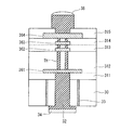
図1において、積層型半導体装置10は、4つのメモリチップ(以下、チップC1〜チップC4とする)と、SOCチップ(以下、チップC0とする)と、パッケージ基板11と、を備えている。
チップC0及びチップC1〜チップC4は、パッケージ基板11上に積層されており、封止樹脂12で封止されている。すなわち、パッケージ基板11は、複数の半導体チップを実装し、複数の半導体チップ及びパッケージ基板11が同一の封止樹脂12によって封止されている。なお、チップC0に積層されるチップの数は4つに限定されるものではない。また、以下では、チップC0〜C4は、フェースダウン型で互いに積層されていることとして、本実施形態の積層型半導体装置10について説明するが、チップC0〜C4の積層形態はフェースダウン型に限定されるものではなく、フェースアップ型であっても構わない。
また、パッケージ基板11において、封止樹脂12で覆われている面の反対側の面には、一群の外部接続端子TEが形成されている。一群の外部接続端子TE各々は、例えば、半田ボールであり、積層型半導体装置10と外部装置(図1において不図示)とを電気的に接続する。
さらに、チップC0の貫通電極TSVは、チップC0の表面側に設けられたバンプ電極13、及びパッケージ基板11の再配線層(図1において不図示)を介して、一群の外部接続端子TEに接続される。このようにして、チップC1〜チップC4は、チップC0、及び一群の外部接続端子TEを介して積層型半導体装置10の外部にある外部装置、例えば、CPU等の演算装置やテスト動作時においては、テスト装置と接続され、チップC0の制御のもと、各チップにおける動作を実行する。
チップC1〜チップC4に形成された複数の貫通電極TSVのうち、チップC0の貫通電極TSV’とバンプ電極13を介して図中縦方向に接続される複数の貫通電極TSVは、貫通電極TSV’、及び複数のバンプ電極13とともに、4群の貫通電極TSV ch A〜TSV ch Dを構成する。また、チップC1〜チップC4に形成された複数の貫通電極TSVのうち、チップC0の貫通電極TSVとバンプ電極13を介して図中縦方向に接続される複数の貫通電極TSVは、貫通電極TSV、及び複数のバンプ電極13とともに、1群の貫通電極TSV DAを構成する。
また、貫通電極TSVS2は、チップC0の内部の制御回路を介さずに貫通電極TSVMと接続されるものであり、例えば、上述のチップC0の1群の貫通電極TSV DAを構成する貫通電極TSVに対応する。
また、貫通電極TSVM2は、平面視で異なる位置に設けられた他チップの貫通電極TSVM2と短絡されている。この種の貫通電極TSVM2に対しては、各チップにおいて平面視で所定の位置に設けられた貫通電極TSVM2aに各チップの内部回路が接続されている。これにより、各チップに設けられた内部回路に対して選択的に情報を入力することが可能となる。例えば、上述の4群の貫通電極TSV ch A〜TSV ch Dの一部であり、後述のチップセレクト信号、テストチップセレクト信号、クロックイネーブル信号、及び、テストクロックイネーブル信号を伝送する貫通電極が貫通電極TSVM2に相当する。
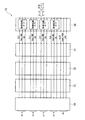
ワイドIODRAMとは、複数のDRAM(Dynamic Random Access Memory)を1つの半導体チップ(以下、単にチップと呼ぶことがある)上に配置して構成したものである。チップ上のDRAMは、それぞれチャネルと呼ばれる。つまり、図4は、4つのDRAMをそれぞれチャネルch A〜チャネルch DとするワイドIODRAMを、チップC0上に4つ積層した積層型半導体装置10の一例を示している。なお、1チップにおけるDRAM(つまり、チャネル)の個数は4個に限られるものではない。
図4において、1つのチップにおけるチャネルch A〜チャネルch Dには、チップC0から、それぞれ互いに独立にデータDQ、コマンド並びにアドレス(アドレス信号Add/コマンド信号CMD)、及びクロック信号CLK等の制御信号が供給される。この構成により、1つのチップのチャネルch A〜チャネルch D各々は、チップC0に配置された制御回路(制御回路ch A〜制御回路ch D)の制御により、例えば、リード動作、ライト動作、リフレッシュ動作などの各種動作を独立に実行することができる。
また、図4に示すように、複数のチップ間において、同一のチャネル同士では、データDQ、コマンド並びにアドレス(アドレス信号Add/コマンド信号CMD)、及び、クロック信号CLK等の制御信号が、各チャネルに対応して設けられた制御回路から共通に供給される。
図4で示した4つのチャネルch A〜チャネルch Dは、図5に示すように平面的に2×2の行列状に配置されている。
各チャネルが形成される領域には、各チャネルに対応する内部制御回路やメモリセルアレイを含む記憶領域部等(図5において不図示)が形成される。
つまり、図1に示した4群の貫通電極TSV ch A〜貫通電極TSV ch Dが、それぞれ対応するチャネルが形成される領域の貫通電極アレイに配置される。例えば、複数の貫通電極TSV ch Aは、チャネルch Aが形成される領域に隣接したTSVアレイ(ch A &DA)に配置される。他の3群の貫通電極TSV ch B〜貫通電極TSV ch Dについても、同様に各チャネルが形成される領域に隣接したTSVアレイに配置される。また、図1に示す1群の貫通電極TSV DAは、4つのTSVアレイに分割して配置される。
つまり、それぞれのTSVアレイ(ch i &DA)には(i=a,b,c,d)、自身が対応するチャネルの制御信号を転送する1群の貫通電極TSV ch iと、テスト信号を転送する貫通電極TSV DAの一部が配置されることになる。
具体的には、外部のテスト装置のプローブを各パッドに接触させ、テスト装置とメモリチップとの間でテストデータtDQ、テストアドレス並びにテストコマンド(テストアドレス信号tAdd/テストコマンド信号tCMD)、及び、テストクロック信号tCLK等のテスト信号をやり取りさせる。テスト信号をやり取りすることにより、チップC0内のメモリセルアレイにおける各メモリセルにテストデータを書き込み、書き込んだテストデータが正しく読み出されるか否かをテスト装置により判定する。
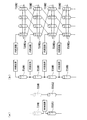
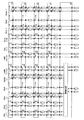
なお、図6において、二重丸で示す符号はチップC1の入出力端子としての貫通電極、表面バンプ及び裏面バンプを包括して示している。以降、図6の説明においては、発明の理解を容易にするためにこれら二重丸で示す符号を単にバンプと呼ぶこともある。また、二重四角で示す符号は、図4に示したテストパッドPadを示す。
また、チップC1は、図1の貫通電極TSV ch Aに対応するノーマルバンプ群nbA(ノーマルアドレスバンプnba 1a−la、ノーマルコマンドバンプnbcm 1a−ma、ノーマルチップセレクトバンプnbcs a1、ノーマルクロックバンプnbck a、ノーマルクロックイネーブルバンプnbcke a1)、ノーマルデータ入出力バンプnbDQ 1a−naを備える。これらのノーマルバンプは、チャネルch Aに接続される。
同様に、チップC1は、貫通電極TSV ch B〜チャネルch Dに対応するノーマルバンプ群nbB、ノーマルデータ入出力バンプnbDQ 1b−nb、ノーマルバンプ群nbC、ノーマルデータ入出力バンプnbDQ 1c−nc、ノーマルバンプ群nbD、ノーマルデータ入出力バンプnbDQ 1d−ndを備える。これらのノーマルバンプは、チャネルchB〜チャネルch Dに接続される。ここで、ノーマルバンプ群nbB、ノーマルバンプ群nbC、及び、ノーマルバンプ群nbDは、ノーマルバンプ群nbAと同じ機能の複数のバンプを含むものとする。また、ノーマルデータ入出力バンプnbDQ 1c−nc、ノーマルデータ入出力バンプnbDQ 1c−nc、及び、ノーマルデータ入出力バンプnbDQ 1d−ndは、ノーマルデータ入出力バンプnbDQ 1a−naと同じ機能の複数のバンプを含むものとする。
ノーマルバンプ群nbAは、チャネルch Aの制御信号入力端子として働くバンプであって、複数のノーマルアドレスバンプnba 1a−la、複数のノーマルコマンドバンプnbcm 1a−ma、ノーマルチップセレクトバンプnbcs a1、ノーマルクロックバンプnbck a、及びノーマルクロックイネーブルバンプnbcke a1を含む。
複数のノーマルアドレスバンプnba 1a−laは、チップ外部から供給される複数のアドレス信号Addを受け取る。
複数のノーマルコマンドバンプnbcm 1a−maは、チップ外部から供給される複数のコマンド信号CMDを受け取る。
ノーマルチップセレクトバンプnbcs a1は、チップ外部から供給されるチップセレクト信号CS(コマンド信号CMDの一部)を受け取る。
ノーマルクロックバンプnbck aは、チップ外部から供給されるクロック信号CLKを受け取る。
ノーマルクロックイネーブルバンプnbcke a1は、チップ外部から供給されるクロックイネーブル信号CKE(クロック信号CLKの一部)を受け取る。
複数のテストアドレスバンプtba 1〜lは、チップ外部から供給される複数のテストアドレス信号tAddを受け取る。
複数のテストコマンドバンプtbcm 1〜mは、チップ外部から供給される複数のテストコマンド信号tCMDを受け取る。
テストチップセレクトバンプtbcs 1は、チップ外部から供給されるテストチップセレクト信号tCS(テストコマンド信号tCMDの一部)を受け取る。
テストクロックバンプtbckは、チップ外部から供給されるテストクロック信号tCLKを受け取る。
テストクロックイネーブルバンプtbcke 1は、チップ外部から供給されるテストクロックイネーブル信号tCKE(テストクロック信号tCLKの一部)を受け取る。
複数のテストアドレスパッドtpa 1〜lは、チップ外部から供給される複数のテストアドレス信号tAddを受け取る。
複数のテストコマンドパッドtpcm 1〜mは、チップ外部から供給される複数のテストコマンド信号tCMDを受け取る。
テストチップセレクトパッドtpcs 1は、チップ外部から供給されるテストチップセレクト信号tCS(テストコマンド信号tCMDの一部)を受け取る。
テストクロックパッドtpckは、チップ外部から供給されるテストクロック信号tCLKを受け取る。
テストクロックイネーブルパッドtpcke 1は、チップ外部から供給されるテストクロックイネーブル信号tCKE(テストクロック信号tCLKの一部)を受け取る。
複数のテストバンプは、例えば、チップC1〜C4をチップC0と積層した後、即ち、複数のテストパッドに外部から直接テスト装置等のプローブを接触させることができないときに、チップC1〜C4のテスト信号入出力端子として用いることができる。上述のとおり、複数のテストバンプは、図1に示す貫通電極TSV DAに対応しているので、複数のテストバンプを備えることで、チップC0と積層した後でも、外部から直接チップC1〜C4にアクセスすることが可能となる。
テスト信号入力部TINUは、チップC1に供給されたテスト信号を各チャネルに共通に供給する部分である。テスト信号入力部TINUは、3個のテスト入力バッファ部tBU a、テスト入力バッファ部tBU cm/cs、及びテスト入力バッファ部tBU ck/ckeを含む。
テスト入力バッファ部tBU aは、各々の入力ノードが、複数のテストアドレスバンプtba 1〜lのうちの対応する1つと複数のテストアドレスパッドtpa 1〜lのうちの対応する1つとの接続ノードt1N1 1〜lに共通に接続された複数のテストアドレス入力バッファを含む。
テスト入力バッファ部tBU cm/csは、各々の入力ノードが、複数のテストコマンドバンプtbcm 1〜m及びテストチップセレクトバンプtbcs 1のうちの対応する1つと複数のテストコマンドパッドtpcm 1〜m及びテストチップセレクトパッドtpcs 1との接続ノードt2N1 1〜m+1に共通に接続された複数のテストコマンド入力バッファを含む。
テスト入力バッファ部tBU ck/ckeは、各々の入力ノードが、テストクロックバンプtbck及びテストクロックイネーブルバンプtbcke 1のうちの対応する1つとテストクロックバンプtbck及びテストクロックイネーブルバンプtbcke 1との接続ノードt3N1 1〜2に共通に接続された2つのテストクロック入力バッファを含む。
言い換えれば、複数のテスト入力端子ペアに含まれる1つのテストバンプと1つのテストパッドとは、チップ内の配線により互いに接続されており、このチップ内配線上のノードが対応するテスト入力バッファの入力ノードに接続されている。
一方、複数のテストテスト入力バッファの出力ノードは、4つのチャネルに共通に接続されている。
チャネルch Aは、3個のノーマル入力バッファ部nBU a、ノーマル入力バッファ部nBU cm/cs、ノーマル入力バッファ部nBU ck/cke、4個のスイッチ回路部SWU21〜スイッチ回路部SWU24、アクセス制御回路41、メモリセルアレイ42、データ入出力回路43、ノーマルデータ入出力バッファ部nBUDQ、及びテストデータ入出力バッファ部tbBUDQを備える。チャネルch B〜チャネルch Dについても、これら各回路を備える。
具体的には、スイッチ回路部SWU21は、それぞれが、ノーマル入力バッファ部nBU aの複数のノーマルアドレス入力バッファのうちの対応する1つの出力ノードとテスト入力バッファ部tBU aの複数のテストアドレス入力バッファのうちの対応する1つの出力ノード(接続ノードt1N2 1〜l)とに接続され、それぞれアドレス信号Add(制御信号)のうちの対応する1つ又はテストアドレス信号tAdd(テスト信号)のうちの対応する1つのいずれか一方を、出力ノードからアクセス制御回路41に供給する複数のスイッチ回路を含む。
メモリセルアレイ42は、複数のメモリセルMCを含む。アクセス制御回路41は、コマンド信号CMD及びチップセレクト信号CS(又はテストコマンド信号tCMD及びテストチップセレクト信号tCS)、及びアドレス信号Add(又はテストアドレス信号tAdd)に応じてメモリセルMCにアクセスし、リード動作ではメモリセルMCが記憶するリードデータをデータ入出力回路43に対して出力させる。また、ライト動作ではデータ入出力回路43が出力するライトデータをメモリセルMCに記憶させる。
データ入出力回路43は、クロック信号CLK(又はテストクロック信号tCLK)に応じて動作し、リード動作時にはメモリセルアレイ42から受け取ったリードデータを、データ入出力部を介してメモリチップ外部に出力し、ライト動作時にはデータ入出力部を介してチップ外部から供給されたライトデータをメモリセルアレイ42に供給する。
1つのノーマルデータ入出力バッファ内において、ノーマルデータ入力バッファnBIDQの入力ノードとノーマルデータ出力バッファnBODQの出力ノードが共通に接続され、このノードをノーマルデータ入出力バッファの第1の接続ノードnBN1(1a−na)とする。
また、1つのノーマルデータ入出力バッファ内において、ノーマルデータ入力バッファnBIDQの出力ノードとノーマルデータ出力バッファnBODQの入力ノードが共通に接続され、このノードをノーマルデータ入出力バッファの第2の接続ノードnBN2(1a−na)とする。ノーマルデータ入出力バッファ部nBUDQの複数のノーマルデータ入出力バッファの第1の接続ノードnBN1(1a−na)は、複数のノーマルデータ入出力バンプnbDQ 1a−naに対応して接続され、第2の接続ノードnBN2は、スイッチ回路部SWU24に接続される。
1つのテストデータ入出力バッファ内において、テストデータ入力バッファtBIDQの入力ノードとテストデータ出力バッファtBODQの出力ノードが共通に接続され、このノードをテストデータ入出力バッファの第1の接続ノードtBN1 1a〜kaとする。
また、1つのテストデータ入出力バッファ内において、テストデータ入力バッファtBIDQの出力ノードとテストデータ出力バッファtBODQの入力ノードが共通に接続され、このノードをテストデータ入出力バッファの第2の接続ノードtBN2 1a〜kaとする。
このように、本実施例のテストデータ入出力バッファ部tBUDQは、各々1つのテストデータ入出力バンプと1つのテストデータ入出力パッドとを含む複数のテストデータ入出力端子ペアに対応して設けられた複数のテストデータ入出力バッファを含み、これら複数のテストデータ入出力バッファの第1の接続ノードが、対応するテストデータ入出力端子ペアに含まれるテストデータ入出力バンプ及びテストデータ入出力パッドと共通に接続されている。
尚、図6では、テストデータ入出力バッファ部tBUDQは、複数のテストデータ入力バッファtBIDQ 1a〜kaと複数のテストデータ出力バッファtBODQ 1a〜kaとの両方を含む構成を示したが、他の構成として、テストデータ入出力バッファ部tBUDQが、複数のテストデータ入力バッファtBIDQ 1a〜kaと複数のテストデータ出力バッファtBODQ 1a〜kaとのいずれか一方のみを含む構成とすることもできる。
スイッチ回路部SWU24に含まれる複数のスイッチ回路それぞれは、リード動作において、データ入出力回路43からの複数のリードデータのうちの対応する1つを受け取り、複数のノーマルデータ入出力バッファのうちの対応する1つ、又は、テストデータ入出力バッファ部tBUDQの複数のテストデータ入出力バッファのうちの対応する1つに供給する。
また、スイッチ回路部SWU24に含まれる複数のスイッチ回路のそれぞれは、ライト動作において、複数のノーマルデータ入出力バッファのうちの対応する1つ、又は、テストデータ入出力バッファ部tBUDQの複数のテストデータ入出力バッファのうちの対応する1つから供給されるライトデータを受け取り、データ入出力回路43に対して供給する。
このように、各チャネルの入力側はテスト用信号を共有する構成となっているが、出力側は、テストデータ入出力パッド及びテストデータ入出力バンプがチャネル毎に独立した構成となっており、テストモードにおいて、テストリードデータの読み出し、テストライトデータの書き込みをチャネル毎に独立に行うことができる。
図7は、チップC0〜C4を積層したときの、各チップ間の接続関係を示す図である。まず、複数のノーマルバンプの接続関係について、説明する。
図7に示すように、チップC1〜C4のそれぞれの、複数のノーマルアドレスバンプnba 1i−li(i=a,b、c、d)、複数のノーマルコマンドバンプnbcm 1i−mi(i=a,b、c、d)、ノーマルクロックバンプnbck i(i=a,b、c、d)、及び、ノーマルデータ入出力バンプnbDQ 1i−ni(i=a,b、c、d)は、それぞれ図2(b)に示した貫通電極TSVM1の型で互いに接続される。また、互いに接続されたノーマルバンプ各々は信号経路(第1の制御信号経路)を構成し、第1の制御信号経路各々は、SOCチップC0の制御回路に接続される。第1の制御信号経路各々は、アドレス信号Add、コマンド信号CMD、クロック信号CLK、及び、データDQをそれぞれ伝送する。
この構成により、通常モード時には、チップC0〜C4のそれぞれのチャネルch A〜ch Dの各々に独立してチップセレクト信号CS及びクロックイネーブル信号CKEを供給することができる。
この構成により、テストモード時には、チップC0〜C4のそれぞれに独立してテストチップセレクト信号tCS及びテストクロックイネーブル信号tCKEを供給することができる。
そのため、本発明によれば、チップC1をチップC0に積層する前と積層する後で別々のテスト信号用の配線を設ける必要はなくなり、積層用半導体装置の半導体チップにテスト端子を配置した際の半導体チップ内の配線の増加を抑制することができる。
続いて、第2の実施形態について説明する。第2の実施形態では、スイッチ回路部SWU21〜スイッチ回路部SWU24と、テストバンプ及びテストバンプとの間に、スイッチ回路部を設け、テストバンプからのテスト信号とテストパッドからのテスト信号とを切り替える構成とした。
図8は、第2の実施形態におけるチップC1の詳細を示すブロック図である。なお、図8において、図6と同一の部分には同一の符号を付し、その説明を適宜省略する。
テスト信号入力部TINUは、図6に示す、3個のテスト入力バッファ部tBU a、テスト入力バッファ部tBU cm/cs、及びテスト入力バッファ部tBU ck/ckeに替えて、以下に説明するテスト入力バッファ部、スイッチ回路部を備える。
すなわち、テスト信号入力部TINUは、4個のテスト入力バッファ部tbBU a、テスト入力バッファ部tpBU a、テスト入力バッファ部tbBU cm、及びテスト入力バッファ部tpBU cmを備える。また、テスト信号入力部TINUは、6個のテスト入力バッファtbBU cs、テスト入力バッファtpBU cs、テスト入力バッファtbBU ck、テスト入力バッファtpBU ck、テスト入力バッファtbBU cke、及びテスト入力バッファtpBU ckeを備える。また、テスト信号入力部TINUは、3個のスイッチ回路部SWU11〜スイッチ回路部SWU13を備える。
テスト入力バッファ部tpBU aは、各々の入力ノードが、複数のテストアドレスパッドtpa 1〜lのうちの対応する1つに接続された複数のテストアドレス入力バッファを含む。
テスト入力バッファ部tbBU cmは、各々の入力ノードが、複数のテストコマンドバンプtbcm 1〜mのうちの対応する1つに接続された複数のテストコマンド入力バッファを含む。
テスト入力バッファ部tpBU cmは、各々の入力ノードが、複数のテストコマンドパッドtpcm 1〜mのうちの対応する1つに接続された複数のテストコマンド入力バッファを含む。
テスト入力バッファtbBU csは、入力ノードが、テストチップセレクトバンプtbcs 1に接続されたテストコマンド入力バッファである。
テスト入力バッファtpBU csは、入力ノードが、テストチップセレクトパッドtpcs 1に接続されたテストコマンド入力バッファである。
テスト入力バッファtbBU ckは、入力ノードが、テストクロックバンプtbckに接続されたテストクロック入力バッファである。
テスト入力バッファtpBU ckは、入力ノードが、テストクロックパッドtpckに接続されたテストクロック入力バッファである。
テスト入力バッファtbBU ckeは、入力ノードが、テストクロックイネーブルバンプtbckeに接続されたテストクロック入力バッファである。
テスト入力バッファtpBU ckeは、入力ノードが、テストクロックイネーブルパッドtpckeに接続されたテストクロック入力バッファである。
具体的には、スイッチ回路部SWU11は、それぞれが、テスト入力バッファ部tbBU aの複数のテストアドレス入力バッファのうちの対応する1つの出力ノードとテスト入力バッファ部tpBU aの複数のテストアドレス入力バッファのうちの対応する1つの出力ノードとに接続される。スイッチ回路部SWU11は、それぞれテストバンプから入力されるテストアドレス信号tAdd(テスト信号)のうちの対応する1つ又はテストパッドから入力されるテストアドレス信号tAddのうちの対応する1つのいずれか一方を、出力ノード(接続ノードt1N2 1〜l)からスイッチ回路部SWU11に供給する複数のスイッチ回路を含む。
また、スイッチ回路部SWU12は、テスト入力バッファtbBU csの出力ノードと、テスト入力バッファtpBU csの出力ノードとに接続される。スイッチ回路部SWU12は、テストバンプから入力されるテストチップセレクト信号tCS(テスト信号)又はテストパッドから入力されるテストチップセレクト信号tCSのいずれか一方を、出力ノード(接続ノードt2N2 m+1)からスイッチ回路部SWU22に供給するスイッチ回路を含む。
また、スイッチ回路部SWU13は、テスト入力バッファtbBUckeの出力ノードとテスト入力バッファtpBUckeの出力ノードとに接続され、テストバンプから入力されるテストクロックイネーブル信号tCKE(テスト信号)又はテストパッドから入力されるテストクロックイネーブル信号tCKEのいずれか一方を、出力ノード(接続ノードt3N2 2)からスイッチ回路部SWU23に供給する。
チャネルch Aはデータ入出力部として、テストデータ入出力バッファ部tBUDQに替えて、テストデータ入出力バッファ部tbBUDQ、テストデータ入出力バッファ部tpBUDQ、及びスイッチ回路部SWU14を備える。
1つのテストデータ入出力バッファ内において、テストデータ入力バッファtbBIDQの入力ノードとテストデータ出力バッファtbBODQの出力ノードが共通に接続され、このノードをテストデータ入出力バッファの第1の接続ノードtbBN1 1a〜kaとする。
また、1つのテストデータ入出力バッファ内において、テストデータ入力バッファtbBIDQの出力ノードとテストデータ出力バッファtbBODQの入力ノードが共通に接続され、このノードをテストデータ入出力バッファの第2の接続ノードtbBN2 1a〜kaとする。
このように、本実施例のテストデータ入出力バッファ部tbBUDQは、複数のテストデータ入出力バンプに対応して設けられた複数のテストデータ入出力バッファを含み、これら複数のテストデータ入出力バッファの第1の接続ノードが、対応するテストデータ入出力バンプと共通に接続されている。
1つのテストデータ入出力バッファ内において、テストデータ入力バッファtpBIDQの入力ノードとテストデータ出力バッファtpBODQの出力ノードが共通に接続され、このノードをテストデータ入出力バッファの第1の接続ノードtpBN1 1a〜kaとする。
また、1つのテストデータ入出力バッファ内において、テストデータ入力バッファtpBIDQの出力ノードとテストデータ出力バッファtpBODQの入力ノードが共通に接続され、このノードをテストデータ入出力バッファの第2の接続ノードtpBN2 1a〜kaとする。
このように、本実施例のテストデータ入出力バッファ部tpBUDQは、複数のテストデータ入出力パッドに対応して設けられた複数のテストデータ入出力バッファを含み、これら複数のテストデータ入出力バッファの第1の接続ノードが、対応するテストデータ入出力パッドと共通に接続されている。
スイッチ回路部SWU14に含まれる複数のスイッチ回路それぞれは、リード動作において、データ入出力回路43からの複数のリードデータのうちの対応する1つをスイッチ回路部SWU24を介して受け取り、テストデータ入出力バッファ部tbBUDQの複数のテストデータ入出力バッファのうちの対応する1つ、又は、テストデータ入出力バッファ部tpBUDQの複数のテストデータ入出力バッファのうちの対応する1つに供給する。
また、スイッチ回路部SWU14に含まれる複数のスイッチ回路のそれぞれは、ライト動作において、テストデータ入出力バッファ部tbBUDQの複数のテストデータ入出力バッファのうちの対応する1つ、又は、テストデータ入出力バッファ部tpBUDQの複数のテストデータ入出力バッファのうちの対応する1つから供給されるライトデータを受け取り、スイッチ回路部SWU24を介してデータ入出力回路43に対して供給する。
例えば、テスト装置からテスト信号のうち、テストアドレス信号tAdd、テストコマンド信号tCMD、テストクロック信号tCLK、及び、テストデータtDQを、図2(b)に示した貫通電極TSVM1の型で互いに接続される第1のテスト信号経路に供給する。
また、テスト装置からテスト信号のうち、テストチップセレクト信号tCSj(j=1〜2,3,4)及びテストクロック信号tCLKの一部としてのテストクロックイネーブル信号tCKEj(j=1,2,3,4)を、それぞれ図2(b)に示した貫通電極TSVM2の型で互いに接続される第2のテスト信号経路(テスト信号経路のうち、チップC1〜チップC4のうち1チップの選択に係るテスト信号が伝達されるテスト信号経路)に供給する。
これにより、積層型半導体装置10において、チップC1〜チップC4のいずれかのチップにおいて、チャネルch A〜チャネルch Dをそれぞれ選択状態にし、例えばテストデータtDQをチャネル間で独立に入出力して、ライトテストまたはリードテストを行うことができる。
本発明の請求の範囲の枠内において種々の開示要素の多様な組み合わせ、ないし選択が可能である。すなわち、本発明は、請求の範囲を含む全開示、技術的思想にしたがって当業者であれば成し得る各種変形、修正を含むことは勿論である。
図9は、ワイヤーボンディング技術を用いてチップを接続した積層型半導体装置10bの概略構成を示す断面図である。
図9において、図1と同様の部分については同じ符号を付し、その説明を省略する。図9に示すように、チップC0における制御回路は、ボンディングワイヤBW NW0により入力端子91(図1におけるバンプ電極13に相当する)が、パッケージ基板11の再配線層(図9において不図示)に接続される。この入力端子91には、外部装置から外部接続端子TEを介して制御信号が供給される。
また、チップC1の入力端子94(図1におけるテスト用のバンプ電極13に相当する)は、ボンディングワイヤBW DAにより、パッケージ基板11の再配線層に接続される。この入力端子94には、外部装置から外部接続端子TEを介してテスト信号が供給される。
Claims (8)
- 第1の半導体チップと、前記第1の半導体チップを制御する制御信号を出力する第2の半導体チップと、を含んで構成される半導体装置であって、
前記第1の半導体チップは、
テスト信号が供給され得るテスト用パッドであって外部端子とは接続されない当該テスト用パッドと、
前記テスト信号が供給され得るテスト端子であって前記第2の半導体チップを介さずに外部端子と接続された当該テスト端子と、
前記テスト信号と前記制御信号とのいずれかを選択する選択回路と、を有し、
前記テスト用パッドと前記テスト端子とが前記選択回路の1つの入力ノードに共通に接続されることを特徴とする半導体装置。 - 前記テスト用パッドと前記テスト端子とから引き出された配線が1つのバッファの入力ノードに共通接続され、当該1つのバッファの出力ノードが、前記選択回路の前記1つの入力ノードである、ことを特徴とする請求項1に記載の半導体装置。
- 前記テスト用パッドから引き出された配線が第1のバッファの入力ノードに接続され、前記テスト端子から引き出された配線が第2のバッファの入力ノードに接続され、
前記第1のバッファの出力ノード、及び前記第2のバッファの出力ノードを入力ノードとし、前記1つの入力ノードを出力ノードとする、前記選択回路の前段に設けられる第2の選択回路を備える、
ことを特徴とする請求項1に記載の半導体装置。 - 前記テスト用パッドは、前記第1の半導体チップが前記第2の半導体チップに積層される前に前記テスト信号が入力されるパッドであり、
前記テスト端子は、前記第1の半導体チップが前記第2の半導体チップに積層された後に前記テスト信号が入力される端子である、
ことを特徴とする請求項1から請求項3いずれか一項に記載の半導体装置。 - 前記テスト端子は、前記第2の半導体チップにおける前記制御信号を出力する制御回路に接続されないテスト信号経路に接続され、当該テスト信号経路に前記テスト信号が外部から供給される、
ことを特徴とする請求項1から請求項4いずれか一項に記載の半導体装置。 - 前記第1の半導体チップは、前記制御信号または前記テスト信号により動作が制御され複数のチャネルを有する半導体チップであって、当該複数のチャネルごとに前記テスト信号経路が設けられる、
ことを特徴とする請求項5に記載の半導体装置。 - 前記第2の半導体チップにおける前記制御信号を出力する制御回路に接続される制御信号経路に接続される前記第1の半導体チップを複数有し、
前記制御信号経路、前記テスト信号経路のうち、前記第1の半導体チップの選択に係る制御信号、及び当該制御信号に対応するテスト信号をそれぞれ伝達する制御信号経路、及びテスト信号経路は複数の前記第1の半導体チップ各々に対して独立に設けられる、
ことを特徴とする請求項6に記載の半導体装置。 - 前記制御信号経路、及び前記テスト信号経路は、前記第1のチップまたは前記第2のチップを裏面側から表面側へと貫通する貫通電極により形成される、
ことを特徴とする請求項7に記載の半導体装置。
Priority Applications (2)
| Application Number | Priority Date | Filing Date | Title |
|---|---|---|---|
| JP2011278311A JP2013131533A (ja) | 2011-12-20 | 2011-12-20 | 半導体装置 |
| US13/720,863 US8957695B2 (en) | 2011-12-20 | 2012-12-19 | Semiconductor device having plural semiconductor chip stacked with one another |
Applications Claiming Priority (1)
| Application Number | Priority Date | Filing Date | Title |
|---|---|---|---|
| JP2011278311A JP2013131533A (ja) | 2011-12-20 | 2011-12-20 | 半導体装置 |
Publications (2)
| Publication Number | Publication Date |
|---|---|
| JP2013131533A true JP2013131533A (ja) | 2013-07-04 |
| JP2013131533A5 JP2013131533A5 (ja) | 2014-12-25 |
Family
ID=48609213
Family Applications (1)
| Application Number | Title | Priority Date | Filing Date |
|---|---|---|---|
| JP2011278311A Withdrawn JP2013131533A (ja) | 2011-12-20 | 2011-12-20 | 半導体装置 |
Country Status (2)
| Country | Link |
|---|---|
| US (1) | US8957695B2 (ja) |
| JP (1) | JP2013131533A (ja) |
Cited By (1)
| Publication number | Priority date | Publication date | Assignee | Title |
|---|---|---|---|---|
| WO2022238798A1 (ja) * | 2021-05-10 | 2022-11-17 | 株式会社半導体エネルギー研究所 | 半導体装置 |
Families Citing this family (13)
| Publication number | Priority date | Publication date | Assignee | Title |
|---|---|---|---|---|
| WO2011156887A1 (en) * | 2010-06-17 | 2011-12-22 | Mosaid Technologies Incorporated | Semiconductor device with through-silicon vias |
| US9859199B2 (en) | 2013-12-18 | 2018-01-02 | Taiwan Semiconductor Manufacturing Co., Ltd. | Method for forming semiconductor package using carbon nano material in molding compound |
| KR20160025957A (ko) * | 2014-08-28 | 2016-03-09 | 에스케이하이닉스 주식회사 | 집적회로 |
| CN107305861B (zh) * | 2016-04-25 | 2019-09-03 | 晟碟信息科技(上海)有限公司 | 半导体装置及其制造方法 |
| US10079049B2 (en) * | 2016-06-08 | 2018-09-18 | Micron Technology, Inc. | Stack access control for memory device |
| US10008287B2 (en) * | 2016-07-22 | 2018-06-26 | Micron Technology, Inc. | Shared error detection and correction memory |
| US9792964B1 (en) * | 2016-09-20 | 2017-10-17 | Micron Technology, Inc. | Apparatus of offset voltage adjustment in input buffer |
| US10282264B1 (en) | 2017-11-09 | 2019-05-07 | Micron Technology, Inc. | Apparatus and methods for repairing memory devices including a plurality of memory die and an interface |
| KR102504332B1 (ko) * | 2018-02-21 | 2023-02-28 | 삼성전자주식회사 | 서로 이격되어 배치되는 범프 어레이들을 포함하는 메모리 장치 및 이를 포함하는 전자 장치 |
| US10664432B2 (en) | 2018-05-23 | 2020-05-26 | Micron Technology, Inc. | Semiconductor layered device with data bus inversion |
| CN109244058A (zh) * | 2018-09-19 | 2019-01-18 | 深圳铨力半导体有限公司 | 半导体封装结构及其制备方法 |
| US10964702B2 (en) | 2018-10-17 | 2021-03-30 | Micron Technology, Inc. | Semiconductor device with first-in-first-out circuit |
| KR20200047930A (ko) | 2018-10-26 | 2020-05-08 | 삼성전자주식회사 | 테스트 패드를 포함하는 반도체 패키지 |
Family Cites Families (2)
| Publication number | Priority date | Publication date | Assignee | Title |
|---|---|---|---|---|
| JP2008140530A (ja) * | 2006-12-05 | 2008-06-19 | Toshiba Corp | 半導体装置およびそのテスト方法 |
| KR100909969B1 (ko) * | 2007-06-28 | 2009-07-29 | 삼성전자주식회사 | 반도체 소자 및 그 제조 방법, 및 반도체 소자를 포함하는스택 모듈, 카드 및 시스템 |
-
2011
- 2011-12-20 JP JP2011278311A patent/JP2013131533A/ja not_active Withdrawn
-
2012
- 2012-12-19 US US13/720,863 patent/US8957695B2/en not_active Expired - Fee Related
Cited By (1)
| Publication number | Priority date | Publication date | Assignee | Title |
|---|---|---|---|---|
| WO2022238798A1 (ja) * | 2021-05-10 | 2022-11-17 | 株式会社半導体エネルギー研究所 | 半導体装置 |
Also Published As
| Publication number | Publication date |
|---|---|
| US20130153898A1 (en) | 2013-06-20 |
| US8957695B2 (en) | 2015-02-17 |
Similar Documents
| Publication | Publication Date | Title |
|---|---|---|
| JP2013131533A (ja) | 半導体装置 | |
| US10037971B2 (en) | Semiconductor device having plural memory chip | |
| JP5932324B2 (ja) | 半導体装置及びその試験方法 | |
| US8981808B2 (en) | Semiconductor device and test method thereof | |
| US8384432B2 (en) | Semiconductor device and information processing system including the same | |
| US20120262196A1 (en) | Semiconductor device including plural core chips and interface chip that controls the core chips and control method thereof | |
| US8952498B2 (en) | Semiconductor device having plural stacked chips | |
| JP5623088B2 (ja) | 半導体装置及びそのテスト方法並びにシステム | |
| JP2012255704A (ja) | 半導体装置 | |
| US20150270250A1 (en) | Semiconductor device | |
| JP5647014B2 (ja) | 半導体装置 | |
| US20130258788A1 (en) | Semiconductor device having plural chip connected to each other | |
| JP2013197576A (ja) | 半導体装置 | |
| CN112562770A (zh) | 具有测试电路的半导体装置 | |
| US9171588B2 (en) | Semiconductor device capable of performing a read leveling and a write leveling based on an ambient temperature | |
| KR20210080928A (ko) | 적층형 반도체 장치 및 이의 테스트 방법 | |
| KR102295895B1 (ko) | 반도체 장치 및 시스템 | |
| US20150226784A1 (en) | Semiconductor device having plural memory units and test method therefor | |
| JP2013131282A (ja) | 半導体装置 | |
| US20180053535A1 (en) | Memory device and central processing unit | |
| WO2014175057A1 (ja) | 半導体装置 | |
| JP2015170370A (ja) | 半導体装置 | |
| JP2016012646A (ja) | 半導体装置 | |
| JP2013131283A (ja) | 半導体装置 | |
| JP2016091576A (ja) | 半導体装置 |
Legal Events
| Date | Code | Title | Description |
|---|---|---|---|
| A711 | Notification of change in applicant |
Free format text: JAPANESE INTERMEDIATE CODE: A711 Effective date: 20130731 |
|
| A521 | Request for written amendment filed |
Free format text: JAPANESE INTERMEDIATE CODE: A821 Effective date: 20130801 |
|
| A521 | Request for written amendment filed |
Free format text: JAPANESE INTERMEDIATE CODE: A523 Effective date: 20130905 |
|
| RD03 | Notification of appointment of power of attorney |
Free format text: JAPANESE INTERMEDIATE CODE: A7423 Effective date: 20131030 |
|
| RD04 | Notification of resignation of power of attorney |
Free format text: JAPANESE INTERMEDIATE CODE: A7424 Effective date: 20131213 |
|
| A521 | Request for written amendment filed |
Free format text: JAPANESE INTERMEDIATE CODE: A523 Effective date: 20141107 |
|
| A621 | Written request for application examination |
Free format text: JAPANESE INTERMEDIATE CODE: A621 Effective date: 20141107 |
|
| A761 | Written withdrawal of application |
Free format text: JAPANESE INTERMEDIATE CODE: A761 Effective date: 20141219 |