JP2013073660A - 半導体装置 - Google Patents
半導体装置 Download PDFInfo
- Publication number
- JP2013073660A JP2013073660A JP2011213698A JP2011213698A JP2013073660A JP 2013073660 A JP2013073660 A JP 2013073660A JP 2011213698 A JP2011213698 A JP 2011213698A JP 2011213698 A JP2011213698 A JP 2011213698A JP 2013073660 A JP2013073660 A JP 2013073660A
- Authority
- JP
- Japan
- Prior art keywords
- signal
- inverter
- output
- circuit
- input
- Prior art date
- Legal status (The legal status is an assumption and is not a legal conclusion. Google has not performed a legal analysis and makes no representation as to the accuracy of the status listed.)
- Abandoned
Links
- 239000004065 semiconductor Substances 0.000 title claims abstract description 19
- 101100452680 Arabidopsis thaliana INVC gene Proteins 0.000 abstract description 18
- 101100508840 Daucus carota INV3 gene Proteins 0.000 abstract description 16
- 101150110971 CIN7 gene Proteins 0.000 abstract description 7
- 101100286980 Daucus carota INV2 gene Proteins 0.000 abstract description 7
- 101150110298 INV1 gene Proteins 0.000 abstract description 7
- 101100397044 Xenopus laevis invs-a gene Proteins 0.000 abstract description 7
- 101100397045 Xenopus laevis invs-b gene Proteins 0.000 abstract description 7
- 230000000295 complement effect Effects 0.000 abstract description 6
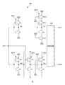
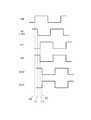
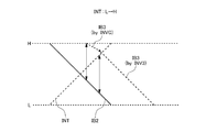
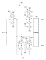
- 238000010586 diagram Methods 0.000 description 18
- 101150070189 CIN3 gene Proteins 0.000 description 11
- 102100030373 HSPB1-associated protein 1 Human genes 0.000 description 4
- 101000843045 Homo sapiens HSPB1-associated protein 1 Proteins 0.000 description 4
- 230000015572 biosynthetic process Effects 0.000 description 4
- 238000003786 synthesis reaction Methods 0.000 description 4
- 238000006243 chemical reaction Methods 0.000 description 2
- 230000006870 function Effects 0.000 description 2
- 238000004519 manufacturing process Methods 0.000 description 2
- 238000000034 method Methods 0.000 description 2
- 230000004048 modification Effects 0.000 description 2
- 238000012986 modification Methods 0.000 description 2
- 230000010363 phase shift Effects 0.000 description 2
- 239000003990 capacitor Substances 0.000 description 1
- 230000007423 decrease Effects 0.000 description 1
- 230000003111 delayed effect Effects 0.000 description 1
- 229910044991 metal oxide Inorganic materials 0.000 description 1
- 150000004706 metal oxides Chemical class 0.000 description 1
- 230000000630 rising effect Effects 0.000 description 1
- 230000001360 synchronised effect Effects 0.000 description 1
Images


Classifications
-
- H—ELECTRICITY
- H03—ELECTRONIC CIRCUITRY
- H03K—PULSE TECHNIQUE
- H03K5/00—Manipulating of pulses not covered by one of the other main groups of this subclass
- H03K5/15—Arrangements in which pulses are delivered at different times at several outputs, i.e. pulse distributors
- H03K5/151—Arrangements in which pulses are delivered at different times at several outputs, i.e. pulse distributors with two complementary outputs
Landscapes
- Physics & Mathematics (AREA)
- Nonlinear Science (AREA)
- Dram (AREA)
- Manipulation Of Pulses (AREA)
Priority Applications (2)
| Application Number | Priority Date | Filing Date | Title |
|---|---|---|---|
| JP2011213698A JP2013073660A (ja) | 2011-09-29 | 2011-09-29 | 半導体装置 |
| US13/610,541 US8653874B2 (en) | 2011-09-29 | 2012-09-11 | Semiconductor device generates complementary output signals |
Applications Claiming Priority (1)
| Application Number | Priority Date | Filing Date | Title |
|---|---|---|---|
| JP2011213698A JP2013073660A (ja) | 2011-09-29 | 2011-09-29 | 半導体装置 |
Publications (2)
| Publication Number | Publication Date |
|---|---|
| JP2013073660A true JP2013073660A (ja) | 2013-04-22 |
| JP2013073660A5 JP2013073660A5 (enExample) | 2014-11-13 |
Family
ID=47991981
Family Applications (1)
| Application Number | Title | Priority Date | Filing Date |
|---|---|---|---|
| JP2011213698A Abandoned JP2013073660A (ja) | 2011-09-29 | 2011-09-29 | 半導体装置 |
Country Status (2)
| Country | Link |
|---|---|
| US (1) | US8653874B2 (enExample) |
| JP (1) | JP2013073660A (enExample) |
Families Citing this family (3)
| Publication number | Priority date | Publication date | Assignee | Title |
|---|---|---|---|---|
| KR20140146368A (ko) * | 2013-06-17 | 2014-12-26 | 에스케이하이닉스 주식회사 | 입출력 장치 및 이를 포함하는 입출력 시스템 |
| EP3934096A1 (en) * | 2020-06-29 | 2022-01-05 | Ams Ag | Driver circuit for low voltage differential signaling, lvds, line driver arrangement for lvds and method for operating an lvds driver circuit |
| US20250300645A1 (en) * | 2024-03-21 | 2025-09-25 | Taiwan Semiconductor Manufacturing Company, Ltd. | System, Device, and Method for Transforming a Single-Ended Input Signal Into Differential Output Signals |
Family Cites Families (8)
| Publication number | Priority date | Publication date | Assignee | Title |
|---|---|---|---|---|
| KR100263485B1 (ko) * | 1998-04-25 | 2000-08-01 | 김영환 | 위상 분리기 |
| US6304122B1 (en) * | 2000-08-17 | 2001-10-16 | International Business Machines Corporation | Low power LSSD flip flops and a flushable single clock splitter for flip flops |
| US6420920B1 (en) * | 2000-08-28 | 2002-07-16 | Micron Technology, Inc. | Method and apparatus for phase-splitting a clock signal |
| KR100432883B1 (ko) * | 2001-12-18 | 2004-05-22 | 삼성전자주식회사 | 클럭 듀티/스큐 보정 기능을 갖는 위상 분주 회로 |
| US6664836B1 (en) * | 2002-12-12 | 2003-12-16 | International Business Machines Corporation | Dynamic phase splitter circuit and method for low-noise and simultaneous production of true and complement dynamic logic signals |
| KR101120047B1 (ko) * | 2007-04-25 | 2012-03-23 | 삼성전자주식회사 | 단일 신호-차동 신호 변환기 및 변환 방법 |
| KR100892647B1 (ko) * | 2007-08-13 | 2009-04-09 | 주식회사 하이닉스반도체 | 반도체 메모리 장치의 클럭 생성 회로 |
| JP4600467B2 (ja) | 2007-12-03 | 2010-12-15 | 富士通セミコンダクター株式会社 | 電子装置及びダブル・データ・レート・シンクロナス・ダイナミック・ランダム・アクセス・メモリ |
-
2011
- 2011-09-29 JP JP2011213698A patent/JP2013073660A/ja not_active Abandoned
-
2012
- 2012-09-11 US US13/610,541 patent/US8653874B2/en not_active Expired - Fee Related
Also Published As
| Publication number | Publication date |
|---|---|
| US8653874B2 (en) | 2014-02-18 |
| US20130082743A1 (en) | 2013-04-04 |
Similar Documents
| Publication | Publication Date | Title |
|---|---|---|
| JP5624441B2 (ja) | 半導体装置 | |
| US7463534B2 (en) | Write apparatus for DDR SDRAM semiconductor memory device | |
| US9166579B2 (en) | Methods and apparatuses for shifting data signals to match command signal delay | |
| CN111554332B (zh) | 使用内部电压为时钟树电路供电 | |
| US9142276B2 (en) | Semiconductor device including latency counter | |
| US8890584B2 (en) | Semiconductor device having gear down mode, method of controlling same, and information processing system | |
| JP2009140322A (ja) | タイミング制御回路および半導体記憶装置 | |
| US10878865B2 (en) | Memory device and signal transmitting circuit thereof | |
| US8553489B2 (en) | Semiconductor device having point-shift type FIFO circuit | |
| US8856577B2 (en) | Semiconductor device having multiplexer | |
| US9041436B2 (en) | Semiconductor device having pull-up circuit and pull-down circuit | |
| JP2013073660A (ja) | 半導体装置 | |
| JP4953273B2 (ja) | 半導体メモリ素子 | |
| WO2014148372A1 (ja) | 半導体装置 | |
| US8384433B2 (en) | Semiconductor device generating complementary output signals | |
| US9590596B1 (en) | Receiving circuit, semiconductor apparatus and system using the same | |
| US8598931B2 (en) | Delay circuit | |
| JP2014158200A (ja) | 半導体装置 | |
| JP2013021404A (ja) | 半導体装置 | |
| JP2013093513A (ja) | 半導体装置 | |
| JP2013236157A (ja) | 入力回路及び半導体装置 | |
| KR20080051835A (ko) | 반도체 메모리 장치의 데이터 입출력 제어 신호 생성 회로 | |
| JP2014207036A (ja) | 半導体装置 | |
| KR20120004682A (ko) | 반도체 메모리 장치 |
Legal Events
| Date | Code | Title | Description |
|---|---|---|---|
| A711 | Notification of change in applicant |
Free format text: JAPANESE INTERMEDIATE CODE: A711 Effective date: 20131029 |
|
| A711 | Notification of change in applicant |
Free format text: JAPANESE INTERMEDIATE CODE: A711 Effective date: 20131030 |
|
| A521 | Request for written amendment filed |
Free format text: JAPANESE INTERMEDIATE CODE: A523 Effective date: 20140925 |
|
| A621 | Written request for application examination |
Free format text: JAPANESE INTERMEDIATE CODE: A621 Effective date: 20140925 |
|
| A762 | Written abandonment of application |
Free format text: JAPANESE INTERMEDIATE CODE: A762 Effective date: 20150108 |