JP2012248682A - 光電変換装置及び光電変換装置の製造方法 - Google Patents
光電変換装置及び光電変換装置の製造方法 Download PDFInfo
- Publication number
- JP2012248682A JP2012248682A JP2011119260A JP2011119260A JP2012248682A JP 2012248682 A JP2012248682 A JP 2012248682A JP 2011119260 A JP2011119260 A JP 2011119260A JP 2011119260 A JP2011119260 A JP 2011119260A JP 2012248682 A JP2012248682 A JP 2012248682A
- Authority
- JP
- Japan
- Prior art keywords
- photoelectric conversion
- insulating film
- conversion device
- shielding film
- light shielding
- Prior art date
- Legal status (The legal status is an assumption and is not a legal conclusion. Google has not performed a legal analysis and makes no representation as to the accuracy of the status listed.)
- Granted
Links
- 238000006243 chemical reaction Methods 0.000 title claims abstract description 127
- 238000004519 manufacturing process Methods 0.000 title claims description 34
- 238000000034 method Methods 0.000 title claims description 33
- 238000001514 detection method Methods 0.000 claims abstract description 56
- 239000000758 substrate Substances 0.000 claims description 40
- 238000005530 etching Methods 0.000 claims description 21
- 238000003384 imaging method Methods 0.000 claims description 20
- 230000008569 process Effects 0.000 claims description 11
- 238000000059 patterning Methods 0.000 claims description 4
- 239000004065 semiconductor Substances 0.000 description 87
- 239000010410 layer Substances 0.000 description 57
- 229910052751 metal Inorganic materials 0.000 description 21
- 239000002184 metal Substances 0.000 description 21
- 229920002120 photoresistant polymer Polymers 0.000 description 18
- 229910052581 Si3N4 Inorganic materials 0.000 description 7
- VYPSYNLAJGMNEJ-UHFFFAOYSA-N Silicium dioxide Chemical compound O=[Si]=O VYPSYNLAJGMNEJ-UHFFFAOYSA-N 0.000 description 7
- HQVNEWCFYHHQES-UHFFFAOYSA-N silicon nitride Chemical compound N12[Si]34N5[Si]62N3[Si]51N64 HQVNEWCFYHHQES-UHFFFAOYSA-N 0.000 description 7
- 229910052814 silicon oxide Inorganic materials 0.000 description 7
- 230000003321 amplification Effects 0.000 description 5
- 238000005468 ion implantation Methods 0.000 description 5
- 238000003199 nucleic acid amplification method Methods 0.000 description 5
- 210000001747 pupil Anatomy 0.000 description 5
- 230000003287 optical effect Effects 0.000 description 4
- WFKWXMTUELFFGS-UHFFFAOYSA-N tungsten Chemical compound [W] WFKWXMTUELFFGS-UHFFFAOYSA-N 0.000 description 4
- 229910052721 tungsten Inorganic materials 0.000 description 4
- 239000010937 tungsten Substances 0.000 description 4
- 238000005229 chemical vapour deposition Methods 0.000 description 3
- 238000010586 diagram Methods 0.000 description 3
- 238000005268 plasma chemical vapour deposition Methods 0.000 description 3
- 230000001681 protective effect Effects 0.000 description 3
- 239000011347 resin Substances 0.000 description 3
- 229920005989 resin Polymers 0.000 description 3
- XUIMIQQOPSSXEZ-UHFFFAOYSA-N Silicon Chemical compound [Si] XUIMIQQOPSSXEZ-UHFFFAOYSA-N 0.000 description 2
- 238000009792 diffusion process Methods 0.000 description 2
- 230000004907 flux Effects 0.000 description 2
- 238000002955 isolation Methods 0.000 description 2
- 239000000463 material Substances 0.000 description 2
- 239000007769 metal material Substances 0.000 description 2
- 230000004048 modification Effects 0.000 description 2
- 238000012986 modification Methods 0.000 description 2
- 229910052710 silicon Inorganic materials 0.000 description 2
- 239000010703 silicon Substances 0.000 description 2
- 240000006829 Ficus sundaica Species 0.000 description 1
- OAICVXFJPJFONN-UHFFFAOYSA-N Phosphorus Chemical compound [P] OAICVXFJPJFONN-UHFFFAOYSA-N 0.000 description 1
- 229910052785 arsenic Inorganic materials 0.000 description 1
- RQNWIZPPADIBDY-UHFFFAOYSA-N arsenic atom Chemical compound [As] RQNWIZPPADIBDY-UHFFFAOYSA-N 0.000 description 1
- 230000004888 barrier function Effects 0.000 description 1
- 230000015572 biosynthetic process Effects 0.000 description 1
- 239000005380 borophosphosilicate glass Substances 0.000 description 1
- 230000000593 degrading effect Effects 0.000 description 1
- 239000012535 impurity Substances 0.000 description 1
- 229910010272 inorganic material Inorganic materials 0.000 description 1
- 239000011147 inorganic material Substances 0.000 description 1
- 238000009413 insulation Methods 0.000 description 1
- 239000011229 interlayer Substances 0.000 description 1
- 239000011368 organic material Substances 0.000 description 1
- 229910052698 phosphorus Inorganic materials 0.000 description 1
- 239000011574 phosphorus Substances 0.000 description 1
- 230000009467 reduction Effects 0.000 description 1
- 238000000926 separation method Methods 0.000 description 1
- HBMJWWWQQXIZIP-UHFFFAOYSA-N silicon carbide Chemical compound [Si+]#[C-] HBMJWWWQQXIZIP-UHFFFAOYSA-N 0.000 description 1
- 229910010271 silicon carbide Inorganic materials 0.000 description 1
- 238000002834 transmittance Methods 0.000 description 1
Images


Classifications
-
- H—ELECTRICITY
- H10—SEMICONDUCTOR DEVICES; ELECTRIC SOLID-STATE DEVICES NOT OTHERWISE PROVIDED FOR
- H10F—INORGANIC SEMICONDUCTOR DEVICES SENSITIVE TO INFRARED RADIATION, LIGHT, ELECTROMAGNETIC RADIATION OF SHORTER WAVELENGTH OR CORPUSCULAR RADIATION
- H10F39/00—Integrated devices, or assemblies of multiple devices, comprising at least one element covered by group H10F30/00, e.g. radiation detectors comprising photodiode arrays
- H10F39/80—Constructional details of image sensors
- H10F39/802—Geometry or disposition of elements in pixels, e.g. address-lines or gate electrodes
- H10F39/8027—Geometry of the photosensitive area
-
- H—ELECTRICITY
- H10—SEMICONDUCTOR DEVICES; ELECTRIC SOLID-STATE DEVICES NOT OTHERWISE PROVIDED FOR
- H10F—INORGANIC SEMICONDUCTOR DEVICES SENSITIVE TO INFRARED RADIATION, LIGHT, ELECTROMAGNETIC RADIATION OF SHORTER WAVELENGTH OR CORPUSCULAR RADIATION
- H10F39/00—Integrated devices, or assemblies of multiple devices, comprising at least one element covered by group H10F30/00, e.g. radiation detectors comprising photodiode arrays
- H10F39/80—Constructional details of image sensors
- H10F39/803—Pixels having integrated switching, control, storage or amplification elements
-
- H—ELECTRICITY
- H10—SEMICONDUCTOR DEVICES; ELECTRIC SOLID-STATE DEVICES NOT OTHERWISE PROVIDED FOR
- H10F—INORGANIC SEMICONDUCTOR DEVICES SENSITIVE TO INFRARED RADIATION, LIGHT, ELECTROMAGNETIC RADIATION OF SHORTER WAVELENGTH OR CORPUSCULAR RADIATION
- H10F39/00—Integrated devices, or assemblies of multiple devices, comprising at least one element covered by group H10F30/00, e.g. radiation detectors comprising photodiode arrays
- H10F39/80—Constructional details of image sensors
- H10F39/805—Coatings
- H10F39/8057—Optical shielding
-
- H—ELECTRICITY
- H10—SEMICONDUCTOR DEVICES; ELECTRIC SOLID-STATE DEVICES NOT OTHERWISE PROVIDED FOR
- H10F—INORGANIC SEMICONDUCTOR DEVICES SENSITIVE TO INFRARED RADIATION, LIGHT, ELECTROMAGNETIC RADIATION OF SHORTER WAVELENGTH OR CORPUSCULAR RADIATION
- H10F39/00—Integrated devices, or assemblies of multiple devices, comprising at least one element covered by group H10F30/00, e.g. radiation detectors comprising photodiode arrays
- H10F39/80—Constructional details of image sensors
- H10F39/806—Optical elements or arrangements associated with the image sensors
- H10F39/8063—Microlenses
Landscapes
- Solid State Image Pick-Up Elements (AREA)
- Light Receiving Elements (AREA)
- Focusing (AREA)
- Automatic Focus Adjustment (AREA)
- Transforming Light Signals Into Electric Signals (AREA)
Abstract
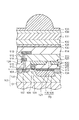
【解決手段】 それぞれが光電変換素子を含む複数の焦点検出用の画素と、光電変換素子で生じた信号を読み出すための複数の配線層とを有する光電変換装置は、複数の配線層の最下層の配線層の下面に比べて、光電変換素子の受光面を含み受光面に平行な面に近接した下面を有し、光電変換素子の一部の上を覆う遮光膜を含む。
【選択図】 図1
Description
そこで、本発明においては精度よく焦点検出を行うための遮光膜の構成及びその製造方法について提供する。
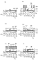
本発明の光電変換装置の製造方法は、それぞれ光電変換素子を含む複数の焦点検出用の画素と、前記光電変換素子で生じた信号を読み出すための複数の配線層とを有する光電変換装置の製造方法において、前記光電変換素子を覆う絶縁膜を形成する工程と、コンタクトホールを前記絶縁膜に形成する工程と、前記コンタクトホールにコンタクトプラグを形成する工程と、前記光電変換素子の一部を覆う溝を前記絶縁膜に形成する工程と、前記溝に不透明膜を形成する工程と、を有する。
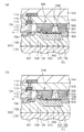
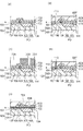
また、本発明の光電変換装置の製造方法は、それぞれが光電変換素子を含む複数の焦点検出用の画素と、前記光電変換素子で生じた信号を読み出すための複数の配線層とを有する光電変換装置の製造方法において、前記光電変換素子を覆う第1の絶縁膜を形成する工程と、前記第1の絶縁膜を覆う不透明膜を形成する工程と、前記不透明膜をパターニングし、前記光電変換素子の一部を覆う遮光膜を形成する工程と、前記遮光膜を覆う第2の絶縁膜を形成する工程と、前記第2の絶縁膜の上に、前記複数の配線層のうち、最下層の配線層を形成する工程と、を有する。
S 表面
105 半導体領域
120 遮光膜
121 開口
118 配線層
124 下面
122 下面
123 上面
108 ゲート電極
Claims (15)
- それぞれが光電変換素子を含む複数の焦点検出用の画素と、前記光電変換素子で生じた信号を読み出すための複数の配線層とを有する光電変換装置において、
前記複数の配線層の最下層の配線層の下面に比べて、前記光電変換素子の受光面を含み前記受光面に平行な面に近接した下面を有し、前記光電変換素子の一部の上を覆う遮光膜を含む光電変換装置。 - 前記遮光膜は、開口を有し、
前記開口の中心が前記光電変換素子の受光面の中心からオフセットしている請求項1に記載の光電変換装置。 - 前記最下層の配線層の下面と前記遮光膜の上面は同一高さに位置している請求項1あるいは2のいずれかに記載の光電変換装置。
- 前記光電変換装置は、前記最下層の配線層の接続のためのコンタクトプラグを有し、
前記コンタクトプラグの上面と前記遮光膜の上面は同一高さに位置している請求項1乃至3のいずれか1項に記載の光電変換装置。 - 前記コンタクトプラグの上面と下面との距離は、前記遮光膜の上面と下面との距離よりも長い請求項4に記載の光電変換装置。
- 前記焦点検出用の画素は、前記信号を読み出すための転送トランジスタを有し、
前記遮光膜は、前記光電変換素子の一部の上から前記転送トランジスタのゲート電極の少なくとも一部の上に延在している請求項1乃至5のいずれか1項に記載の光電変換装置。 - 前記遮光膜が前記転送トランジスタのドレインの上には延在しない請求項6に記載の光電変換装置。
- 前記光電変換装置は、更に複数の撮像用の画素を有する請求項1乃至7のいずれか1項に記載の光電変換装置。
- 前記光電変換装置は、前記複数の撮像用の画素と前記複数の焦点検出用の画素とに配されたマイクロレンズを有する請求項8に記載の光電変換装置。
- 請求項1乃至9のいずれか1項に記載の光電変換装置と、
前記光電変換装置からの信号を処理する信号処理部と、を有する撮像システム。 - それぞれ光電変換素子を含む複数の焦点検出用の画素と、前記光電変換素子で生じた信号を読み出すための複数の配線層とを有する光電変換装置の製造方法において、
前記光電変換素子を覆う絶縁膜を形成する工程と、
コンタクトホールを前記絶縁膜に形成する工程と、
前記コンタクトホールにコンタクトプラグを形成する工程と、
前記光電変換素子の一部を覆う溝を前記絶縁膜に形成する工程と、
前記溝に不透明膜を形成する工程と、を有する光電変換装置の製造方法。 - 前記絶縁膜の上に前記複数の配線層のうち最下層の配線層を形成する工程を有する請求項11に記載の光電変換装置の製造方法。
- 前記コンタクトホールにコンタクトプラグを形成する工程と、前記絶縁膜に溝を形成する工程と、とが同じ工程で行われる請求項11あるいは12のいずれかに記載の光電変換装置の製造方法。
- それぞれが光電変換素子を含む複数の焦点検出用の画素と、前記光電変換素子で生じた信号を読み出すための複数の配線層とを有する光電変換装置の製造方法において、
前記光電変換素子を覆う第1の絶縁膜を形成する工程と、
前記第1の絶縁膜を覆う不透明膜を形成する工程と、
前記不透明膜をパターニングし、前記光電変換素子の一部を覆う遮光膜を形成する工程と、
前記遮光膜を覆う第2の絶縁膜を形成する工程と、
前記第2の絶縁膜の上に、前記複数の配線層のうち、最下層の配線層を形成する工程と、を有する光電変換装置の製造方法。 - 前記第1の絶縁膜は、前記遮光膜を形成する工程におけるエッチングストップとして機能する請求項14に記載の光電変換装置の製造方法。
Priority Applications (3)
| Application Number | Priority Date | Filing Date | Title |
|---|---|---|---|
| JP2011119260A JP5814626B2 (ja) | 2011-05-27 | 2011-05-27 | 光電変換装置及び光電変換装置の製造方法 |
| US13/473,460 US8754969B2 (en) | 2011-05-27 | 2012-05-16 | Photoelectric conversion apparatus and method of manufacturing photoelectric conversion apparatus |
| CN201210159758.0A CN102800683B (zh) | 2011-05-27 | 2012-05-22 | 光电转换设备和制造光电转换设备的方法 |
Applications Claiming Priority (1)
| Application Number | Priority Date | Filing Date | Title |
|---|---|---|---|
| JP2011119260A JP5814626B2 (ja) | 2011-05-27 | 2011-05-27 | 光電変換装置及び光電変換装置の製造方法 |
Publications (2)
| Publication Number | Publication Date |
|---|---|
| JP2012248682A true JP2012248682A (ja) | 2012-12-13 |
| JP5814626B2 JP5814626B2 (ja) | 2015-11-17 |
Family
ID=47199744
Family Applications (1)
| Application Number | Title | Priority Date | Filing Date |
|---|---|---|---|
| JP2011119260A Expired - Fee Related JP5814626B2 (ja) | 2011-05-27 | 2011-05-27 | 光電変換装置及び光電変換装置の製造方法 |
Country Status (3)
| Country | Link |
|---|---|
| US (1) | US8754969B2 (ja) |
| JP (1) | JP5814626B2 (ja) |
| CN (1) | CN102800683B (ja) |
Cited By (5)
| Publication number | Priority date | Publication date | Assignee | Title |
|---|---|---|---|---|
| JP2014187068A (ja) * | 2013-03-21 | 2014-10-02 | Canon Inc | 固体撮像装置及び撮像システム |
| JP2014187067A (ja) * | 2013-03-21 | 2014-10-02 | Canon Inc | 固体撮像装置及び撮像システム |
| JP2015233043A (ja) * | 2014-06-09 | 2015-12-24 | ソニー株式会社 | 撮像素子および電子機器、並びに製造方法 |
| WO2016031592A1 (ja) * | 2014-08-29 | 2016-03-03 | ソニー株式会社 | 固体撮像装置、および電子装置 |
| WO2016098624A1 (ja) * | 2014-12-18 | 2016-06-23 | ソニー株式会社 | 固体撮像素子、撮像装置、および電子機器 |
Families Citing this family (14)
| Publication number | Priority date | Publication date | Assignee | Title |
|---|---|---|---|---|
| JP2011040647A (ja) * | 2009-08-17 | 2011-02-24 | Hitachi Ltd | 固体撮像素子 |
| WO2012039180A1 (ja) * | 2010-09-24 | 2012-03-29 | 富士フイルム株式会社 | 撮像デバイス及び撮像装置 |
| JP6084922B2 (ja) | 2011-06-23 | 2017-02-22 | パナソニック株式会社 | 固体撮像装置 |
| JP2013145779A (ja) * | 2012-01-13 | 2013-07-25 | Sony Corp | 固体撮像装置及び電子機器 |
| JP5966636B2 (ja) * | 2012-06-06 | 2016-08-10 | 株式会社ニコン | 撮像素子および撮像装置 |
| US9232122B2 (en) * | 2012-09-19 | 2016-01-05 | Lg Innotek Co., Ltd. | Camera module having an array sensor |
| EP2782331A1 (en) * | 2013-03-22 | 2014-09-24 | Harvest Imaging bvba | Image sensor with focus-detection pixel, and method for reading focus-information |
| JP6162999B2 (ja) * | 2013-04-15 | 2017-07-12 | キヤノン株式会社 | 固体撮像装置およびカメラ |
| US20140375852A1 (en) * | 2013-06-20 | 2014-12-25 | Canon Kabushiki Kaisha | Solid-state imaging apparatus, method of manufacturing the same, camera, imaging device, and imaging apparatus |
| US20150062422A1 (en) * | 2013-08-27 | 2015-03-05 | Semiconductor Components Industries, Llc | Lens alignment in camera modules using phase detection pixels |
| JP2015060855A (ja) * | 2013-09-17 | 2015-03-30 | ソニー株式会社 | 固体撮像装置およびその製造方法、並びに電子機器 |
| WO2016194501A1 (ja) * | 2015-06-03 | 2016-12-08 | ソニー株式会社 | 固体撮像素子、撮像装置、及び、固体撮像素子の製造方法 |
| CN107004691B (zh) * | 2015-11-12 | 2022-02-11 | 松下知识产权经营株式会社 | 光检测装置 |
| CN109417080A (zh) * | 2018-09-26 | 2019-03-01 | 深圳市汇顶科技股份有限公司 | 光学图像采集单元、光学图像采集装置和电子设备 |
Citations (5)
| Publication number | Priority date | Publication date | Assignee | Title |
|---|---|---|---|---|
| JP2009099817A (ja) * | 2007-10-18 | 2009-05-07 | Nikon Corp | 固体撮像素子 |
| JP2009105358A (ja) * | 2007-10-01 | 2009-05-14 | Nikon Corp | 固体撮像素子及びこれを用いた電子カメラ |
| US20090303366A1 (en) * | 2008-06-05 | 2009-12-10 | International Business Machines Corporation | Interlevel conductive light shield |
| JP2011003738A (ja) * | 2009-06-18 | 2011-01-06 | Canon Inc | 固体撮像装置及びその製造方法 |
| JP2011029604A (ja) * | 2009-06-26 | 2011-02-10 | Canon Inc | 光電変換装置の製造方法 |
Family Cites Families (9)
| Publication number | Priority date | Publication date | Assignee | Title |
|---|---|---|---|---|
| JP3434740B2 (ja) * | 1999-06-30 | 2003-08-11 | Necエレクトロニクス株式会社 | 固体撮像装置 |
| KR100699897B1 (ko) * | 2006-02-17 | 2007-03-28 | 삼성전자주식회사 | 이미지센서의 제조 방법 |
| JP5157436B2 (ja) | 2007-10-11 | 2013-03-06 | 株式会社ニコン | 固体撮像素子および撮像装置 |
| KR101776955B1 (ko) * | 2009-02-10 | 2017-09-08 | 소니 주식회사 | 고체 촬상 장치와 그 제조 방법, 및 전자 기기 |
| JP5476731B2 (ja) * | 2009-02-13 | 2014-04-23 | 株式会社ニコン | 撮像素子 |
| KR101786069B1 (ko) * | 2009-02-17 | 2017-10-16 | 가부시키가이샤 니콘 | 이면 조사형 촬상 소자, 그 제조 방법 및 촬상 장치 |
| JP5476745B2 (ja) * | 2009-03-05 | 2014-04-23 | ソニー株式会社 | 固体撮像装置とその製造方法、及び電子機器 |
| JP5366616B2 (ja) * | 2009-04-02 | 2013-12-11 | キヤノン株式会社 | 撮像素子及びその製造方法 |
| JP5434761B2 (ja) * | 2010-04-08 | 2014-03-05 | 株式会社ニコン | 撮像デバイスおよび撮像装置 |
-
2011
- 2011-05-27 JP JP2011119260A patent/JP5814626B2/ja not_active Expired - Fee Related
-
2012
- 2012-05-16 US US13/473,460 patent/US8754969B2/en not_active Expired - Fee Related
- 2012-05-22 CN CN201210159758.0A patent/CN102800683B/zh not_active Expired - Fee Related
Patent Citations (5)
| Publication number | Priority date | Publication date | Assignee | Title |
|---|---|---|---|---|
| JP2009105358A (ja) * | 2007-10-01 | 2009-05-14 | Nikon Corp | 固体撮像素子及びこれを用いた電子カメラ |
| JP2009099817A (ja) * | 2007-10-18 | 2009-05-07 | Nikon Corp | 固体撮像素子 |
| US20090303366A1 (en) * | 2008-06-05 | 2009-12-10 | International Business Machines Corporation | Interlevel conductive light shield |
| JP2011003738A (ja) * | 2009-06-18 | 2011-01-06 | Canon Inc | 固体撮像装置及びその製造方法 |
| JP2011029604A (ja) * | 2009-06-26 | 2011-02-10 | Canon Inc | 光電変換装置の製造方法 |
Cited By (11)
| Publication number | Priority date | Publication date | Assignee | Title |
|---|---|---|---|---|
| JP2014187068A (ja) * | 2013-03-21 | 2014-10-02 | Canon Inc | 固体撮像装置及び撮像システム |
| JP2014187067A (ja) * | 2013-03-21 | 2014-10-02 | Canon Inc | 固体撮像装置及び撮像システム |
| JP2015233043A (ja) * | 2014-06-09 | 2015-12-24 | ソニー株式会社 | 撮像素子および電子機器、並びに製造方法 |
| US10263024B2 (en) | 2014-06-09 | 2019-04-16 | Sony Corporation | Imaging element, electronic device, and manufacturing method |
| WO2016031592A1 (ja) * | 2014-08-29 | 2016-03-03 | ソニー株式会社 | 固体撮像装置、および電子装置 |
| US11004877B2 (en) | 2014-08-29 | 2021-05-11 | Sony Corporation | Solid-state imaging device with phase difference detection pixel and electronic apparatus |
| WO2016098624A1 (ja) * | 2014-12-18 | 2016-06-23 | ソニー株式会社 | 固体撮像素子、撮像装置、および電子機器 |
| JPWO2016098624A1 (ja) * | 2014-12-18 | 2017-09-28 | ソニー株式会社 | 固体撮像素子、撮像装置、および電子機器 |
| US9986186B2 (en) | 2014-12-18 | 2018-05-29 | Sony Corporation | Solid-state image sensor, imaging device, and electronic device |
| US10594969B2 (en) | 2014-12-18 | 2020-03-17 | Sony Corporation | Solid-state image sensor, imaging device, and electronic device |
| US11678088B2 (en) | 2014-12-18 | 2023-06-13 | Sony Corporation | Solid-state image sensor, imaging device, and electronic device |
Also Published As
| Publication number | Publication date |
|---|---|
| US8754969B2 (en) | 2014-06-17 |
| JP5814626B2 (ja) | 2015-11-17 |
| US20120300102A1 (en) | 2012-11-29 |
| CN102800683A (zh) | 2012-11-28 |
| CN102800683B (zh) | 2015-06-24 |
Similar Documents
| Publication | Publication Date | Title |
|---|---|---|
| JP5814626B2 (ja) | 光電変換装置及び光電変換装置の製造方法 | |
| US20220190022A1 (en) | Image sensors | |
| US9344653B2 (en) | Solid-state imaging apparatus and imaging system | |
| CN103779369B (zh) | 摄像装置、其制造方法和照相机 | |
| JP5814625B2 (ja) | 固体撮像装置、それを用いた撮像システム及び固体撮像装置の製造方法 | |
| JP5241902B2 (ja) | 半導体装置の製造方法 | |
| JP6021439B2 (ja) | 固体撮像装置 | |
| JP2010062438A (ja) | 固体撮像装置およびその設計方法 | |
| JP5921129B2 (ja) | 固体撮像装置、及び固体撮像装置の製造方法 | |
| US8405178B2 (en) | Solid-state image sensor device | |
| US9515117B2 (en) | Method of manufacturing an image sensor using multiple exposures | |
| US10204943B2 (en) | Image sensor, method of manufacturing the same, and camera with pixel including light waveguide and insulation film | |
| CN105390445A (zh) | 半导体器件制造方法和半导体器件 | |
| US9357186B2 (en) | Solid-state imaging apparatus and camera | |
| KR102581170B1 (ko) | 후면 조사형 이미지 센서 및 그 제조 방법 | |
| US8389923B2 (en) | Photoelectric conversion device, image sensing system, and method of manufacturing photoelectric conversion device | |
| US9086577B2 (en) | Solid-state imaging apparatus and imaging system | |
| JP2013182943A (ja) | 固体撮像装置の製造方法 | |
| JP2009027004A (ja) | 光電変換装置及び光電変換装置を用いた撮像システム | |
| US9929303B2 (en) | Method of manufacturing solid-state image sensor | |
| JP2014086514A (ja) | 撮像装置、その製造方法及びカメラ | |
| US9305950B2 (en) | Solid-state imaging apparatus and imaging system | |
| JP2014086515A (ja) | 撮像装置、その製造方法及びカメラ | |
| JP7008054B2 (ja) | 光電変換装置および機器 | |
| JP2012204686A (ja) | 固体撮像装置及びその製造方法 |
Legal Events
| Date | Code | Title | Description |
|---|---|---|---|
| A621 | Written request for application examination |
Free format text: JAPANESE INTERMEDIATE CODE: A621 Effective date: 20140526 |
|
| A977 | Report on retrieval |
Free format text: JAPANESE INTERMEDIATE CODE: A971007 Effective date: 20150219 |
|
| A131 | Notification of reasons for refusal |
Free format text: JAPANESE INTERMEDIATE CODE: A131 Effective date: 20150303 |
|
| A521 | Request for written amendment filed |
Free format text: JAPANESE INTERMEDIATE CODE: A523 Effective date: 20150416 |
|
| TRDD | Decision of grant or rejection written | ||
| A01 | Written decision to grant a patent or to grant a registration (utility model) |
Free format text: JAPANESE INTERMEDIATE CODE: A01 Effective date: 20150825 |
|
| A61 | First payment of annual fees (during grant procedure) |
Free format text: JAPANESE INTERMEDIATE CODE: A61 Effective date: 20150918 |
|
| R151 | Written notification of patent or utility model registration |
Ref document number: 5814626 Country of ref document: JP Free format text: JAPANESE INTERMEDIATE CODE: R151 |
|
| LAPS | Cancellation because of no payment of annual fees |