JP2012185486A - 表示装置 - Google Patents
表示装置 Download PDFInfo
- Publication number
- JP2012185486A JP2012185486A JP2012025709A JP2012025709A JP2012185486A JP 2012185486 A JP2012185486 A JP 2012185486A JP 2012025709 A JP2012025709 A JP 2012025709A JP 2012025709 A JP2012025709 A JP 2012025709A JP 2012185486 A JP2012185486 A JP 2012185486A
- Authority
- JP
- Japan
- Prior art keywords
- liquid crystal
- display
- light
- crystal element
- panel
- Prior art date
- Legal status (The legal status is an assumption and is not a legal conclusion. Google has not performed a legal analysis and makes no representation as to the accuracy of the status listed.)
- Granted
Links
- 239000004973 liquid crystal related substance Substances 0.000 claims abstract description 166
- 239000010410 layer Substances 0.000 description 108
- 239000010408 film Substances 0.000 description 51
- 239000000758 substrate Substances 0.000 description 45
- 239000004065 semiconductor Substances 0.000 description 35
- 230000003287 optical effect Effects 0.000 description 34
- 238000000034 method Methods 0.000 description 32
- 230000004888 barrier function Effects 0.000 description 21
- 239000000463 material Substances 0.000 description 21
- 229910007541 Zn O Inorganic materials 0.000 description 12
- 238000005401 electroluminescence Methods 0.000 description 12
- 239000011347 resin Substances 0.000 description 9
- 229920005989 resin Polymers 0.000 description 9
- 230000015572 biosynthetic process Effects 0.000 description 8
- 229910021420 polycrystalline silicon Inorganic materials 0.000 description 8
- 239000011701 zinc Substances 0.000 description 8
- 238000010586 diagram Methods 0.000 description 7
- 229920005591 polysilicon Polymers 0.000 description 7
- 239000000565 sealant Substances 0.000 description 7
- XLOMVQKBTHCTTD-UHFFFAOYSA-N Zinc monoxide Chemical compound [Zn]=O XLOMVQKBTHCTTD-UHFFFAOYSA-N 0.000 description 6
- 239000013078 crystal Substances 0.000 description 6
- 229910052733 gallium Inorganic materials 0.000 description 6
- 239000012212 insulator Substances 0.000 description 6
- 229910052750 molybdenum Inorganic materials 0.000 description 6
- 230000008569 process Effects 0.000 description 6
- VYPSYNLAJGMNEJ-UHFFFAOYSA-N silicon dioxide Inorganic materials O=[Si]=O VYPSYNLAJGMNEJ-UHFFFAOYSA-N 0.000 description 6
- 239000010936 titanium Substances 0.000 description 6
- ZOKXTWBITQBERF-UHFFFAOYSA-N Molybdenum Chemical compound [Mo] ZOKXTWBITQBERF-UHFFFAOYSA-N 0.000 description 5
- 229910052581 Si3N4 Inorganic materials 0.000 description 5
- XUIMIQQOPSSXEZ-UHFFFAOYSA-N Silicon Chemical compound [Si] XUIMIQQOPSSXEZ-UHFFFAOYSA-N 0.000 description 5
- 239000000956 alloy Substances 0.000 description 5
- 229910052782 aluminium Inorganic materials 0.000 description 5
- 239000003086 colorant Substances 0.000 description 5
- KPUWHANPEXNPJT-UHFFFAOYSA-N disiloxane Chemical class [SiH3]O[SiH3] KPUWHANPEXNPJT-UHFFFAOYSA-N 0.000 description 5
- 239000011521 glass Substances 0.000 description 5
- 239000011159 matrix material Substances 0.000 description 5
- 239000011733 molybdenum Substances 0.000 description 5
- 238000007789 sealing Methods 0.000 description 5
- 229910052710 silicon Inorganic materials 0.000 description 5
- 239000010703 silicon Substances 0.000 description 5
- HQVNEWCFYHHQES-UHFFFAOYSA-N silicon nitride Chemical compound N12[Si]34N5[Si]62N3[Si]51N64 HQVNEWCFYHHQES-UHFFFAOYSA-N 0.000 description 5
- 229910052814 silicon oxide Inorganic materials 0.000 description 5
- 229910052719 titanium Inorganic materials 0.000 description 5
- 229910052721 tungsten Inorganic materials 0.000 description 5
- RTAQQCXQSZGOHL-UHFFFAOYSA-N Titanium Chemical compound [Ti] RTAQQCXQSZGOHL-UHFFFAOYSA-N 0.000 description 4
- 229910045601 alloy Inorganic materials 0.000 description 4
- XAGFODPZIPBFFR-UHFFFAOYSA-N aluminium Chemical compound [Al] XAGFODPZIPBFFR-UHFFFAOYSA-N 0.000 description 4
- 239000011651 chromium Substances 0.000 description 4
- 239000005262 ferroelectric liquid crystals (FLCs) Substances 0.000 description 4
- 238000004544 sputter deposition Methods 0.000 description 4
- 239000000126 substance Substances 0.000 description 4
- 239000010937 tungsten Substances 0.000 description 4
- 230000000007 visual effect Effects 0.000 description 4
- RYGMFSIKBFXOCR-UHFFFAOYSA-N Copper Chemical compound [Cu] RYGMFSIKBFXOCR-UHFFFAOYSA-N 0.000 description 3
- 229910019092 Mg-O Inorganic materials 0.000 description 3
- 229910019395 Mg—O Inorganic materials 0.000 description 3
- NIXOWILDQLNWCW-UHFFFAOYSA-N acrylic acid group Chemical group C(C=C)(=O)O NIXOWILDQLNWCW-UHFFFAOYSA-N 0.000 description 3
- 230000005540 biological transmission Effects 0.000 description 3
- 239000003990 capacitor Substances 0.000 description 3
- 229910052804 chromium Inorganic materials 0.000 description 3
- 238000000576 coating method Methods 0.000 description 3
- 239000004020 conductor Substances 0.000 description 3
- 229910052802 copper Inorganic materials 0.000 description 3
- 239000010949 copper Substances 0.000 description 3
- 239000007789 gas Substances 0.000 description 3
- 229910052751 metal Inorganic materials 0.000 description 3
- 229910044991 metal oxide Inorganic materials 0.000 description 3
- 150000004706 metal oxides Chemical group 0.000 description 3
- 239000000203 mixture Substances 0.000 description 3
- 239000002356 single layer Substances 0.000 description 3
- 125000006850 spacer group Chemical group 0.000 description 3
- 229910052715 tantalum Inorganic materials 0.000 description 3
- WFKWXMTUELFFGS-UHFFFAOYSA-N tungsten Chemical compound [W] WFKWXMTUELFFGS-UHFFFAOYSA-N 0.000 description 3
- 239000011787 zinc oxide Substances 0.000 description 3
- WZJUBBHODHNQPW-UHFFFAOYSA-N 2,4,6,8-tetramethyl-1,3,5,7,2$l^{3},4$l^{3},6$l^{3},8$l^{3}-tetraoxatetrasilocane Chemical compound C[Si]1O[Si](C)O[Si](C)O[Si](C)O1 WZJUBBHODHNQPW-UHFFFAOYSA-N 0.000 description 2
- UWCWUCKPEYNDNV-LBPRGKRZSA-N 2,6-dimethyl-n-[[(2s)-pyrrolidin-2-yl]methyl]aniline Chemical compound CC1=CC=CC(C)=C1NC[C@H]1NCCC1 UWCWUCKPEYNDNV-LBPRGKRZSA-N 0.000 description 2
- 229910000838 Al alloy Inorganic materials 0.000 description 2
- XKRFYHLGVUSROY-UHFFFAOYSA-N Argon Chemical compound [Ar] XKRFYHLGVUSROY-UHFFFAOYSA-N 0.000 description 2
- IJGRMHOSHXDMSA-UHFFFAOYSA-N Atomic nitrogen Chemical compound N#N IJGRMHOSHXDMSA-UHFFFAOYSA-N 0.000 description 2
- VYZAMTAEIAYCRO-UHFFFAOYSA-N Chromium Chemical compound [Cr] VYZAMTAEIAYCRO-UHFFFAOYSA-N 0.000 description 2
- 239000004593 Epoxy Substances 0.000 description 2
- 229910052779 Neodymium Inorganic materials 0.000 description 2
- BLRPTPMANUNPDV-UHFFFAOYSA-N Silane Chemical compound [SiH4] BLRPTPMANUNPDV-UHFFFAOYSA-N 0.000 description 2
- BOTDANWDWHJENH-UHFFFAOYSA-N Tetraethyl orthosilicate Chemical compound CCO[Si](OCC)(OCC)OCC BOTDANWDWHJENH-UHFFFAOYSA-N 0.000 description 2
- NRTOMJZYCJJWKI-UHFFFAOYSA-N Titanium nitride Chemical compound [Ti]#N NRTOMJZYCJJWKI-UHFFFAOYSA-N 0.000 description 2
- 229910021417 amorphous silicon Inorganic materials 0.000 description 2
- 230000000903 blocking effect Effects 0.000 description 2
- 238000005229 chemical vapour deposition Methods 0.000 description 2
- 230000003098 cholesteric effect Effects 0.000 description 2
- 238000001514 detection method Methods 0.000 description 2
- 230000009977 dual effect Effects 0.000 description 2
- 230000005684 electric field Effects 0.000 description 2
- 230000001747 exhibiting effect Effects 0.000 description 2
- 239000011152 fibreglass Substances 0.000 description 2
- 125000001153 fluoro group Chemical group F* 0.000 description 2
- 238000010438 heat treatment Methods 0.000 description 2
- 229910052738 indium Inorganic materials 0.000 description 2
- AMGQUBHHOARCQH-UHFFFAOYSA-N indium;oxotin Chemical compound [In].[Sn]=O AMGQUBHHOARCQH-UHFFFAOYSA-N 0.000 description 2
- 238000002347 injection Methods 0.000 description 2
- 239000007924 injection Substances 0.000 description 2
- 229910052748 manganese Inorganic materials 0.000 description 2
- 238000004519 manufacturing process Methods 0.000 description 2
- 239000002184 metal Substances 0.000 description 2
- QEFYFXOXNSNQGX-UHFFFAOYSA-N neodymium atom Chemical compound [Nd] QEFYFXOXNSNQGX-UHFFFAOYSA-N 0.000 description 2
- HMMGMWAXVFQUOA-UHFFFAOYSA-N octamethylcyclotetrasiloxane Chemical compound C[Si]1(C)O[Si](C)(C)O[Si](C)(C)O[Si](C)(C)O1 HMMGMWAXVFQUOA-UHFFFAOYSA-N 0.000 description 2
- 125000000962 organic group Chemical group 0.000 description 2
- 239000011368 organic material Substances 0.000 description 2
- 238000005268 plasma chemical vapour deposition Methods 0.000 description 2
- 229920002620 polyvinyl fluoride Polymers 0.000 description 2
- 229910052706 scandium Inorganic materials 0.000 description 2
- SIXSYDAISGFNSX-UHFFFAOYSA-N scandium atom Chemical compound [Sc] SIXSYDAISGFNSX-UHFFFAOYSA-N 0.000 description 2
- 239000003566 sealing material Substances 0.000 description 2
- 229910000077 silane Inorganic materials 0.000 description 2
- 230000007480 spreading Effects 0.000 description 2
- 238000003892 spreading Methods 0.000 description 2
- GUVRBAGPIYLISA-UHFFFAOYSA-N tantalum atom Chemical compound [Ta] GUVRBAGPIYLISA-UHFFFAOYSA-N 0.000 description 2
- CZDYPVPMEAXLPK-UHFFFAOYSA-N tetramethylsilane Chemical compound C[Si](C)(C)C CZDYPVPMEAXLPK-UHFFFAOYSA-N 0.000 description 2
- 238000007740 vapor deposition Methods 0.000 description 2
- 229910052725 zinc Inorganic materials 0.000 description 2
- 239000004925 Acrylic resin Substances 0.000 description 1
- 229920000178 Acrylic resin Polymers 0.000 description 1
- 239000004986 Cholesteric liquid crystals (ChLC) Substances 0.000 description 1
- GYHNNYVSQQEPJS-UHFFFAOYSA-N Gallium Chemical compound [Ga] GYHNNYVSQQEPJS-UHFFFAOYSA-N 0.000 description 1
- 239000005264 High molar mass liquid crystal Substances 0.000 description 1
- OAICVXFJPJFONN-UHFFFAOYSA-N Phosphorus Chemical compound [P] OAICVXFJPJFONN-UHFFFAOYSA-N 0.000 description 1
- 239000004952 Polyamide Substances 0.000 description 1
- 239000004642 Polyimide Substances 0.000 description 1
- 239000004983 Polymer Dispersed Liquid Crystal Substances 0.000 description 1
- 229910000676 Si alloy Inorganic materials 0.000 description 1
- 229910004298 SiO 2 Inorganic materials 0.000 description 1
- 229910002808 Si–O–Si Inorganic materials 0.000 description 1
- 239000004990 Smectic liquid crystal Substances 0.000 description 1
- 229910020923 Sn-O Inorganic materials 0.000 description 1
- 239000004974 Thermotropic liquid crystal Substances 0.000 description 1
- 229910001069 Ti alloy Inorganic materials 0.000 description 1
- GDFCWFBWQUEQIJ-UHFFFAOYSA-N [B].[P] Chemical compound [B].[P] GDFCWFBWQUEQIJ-UHFFFAOYSA-N 0.000 description 1
- 125000000217 alkyl group Chemical group 0.000 description 1
- 229910052786 argon Inorganic materials 0.000 description 1
- 125000003118 aryl group Chemical group 0.000 description 1
- QVGXLLKOCUKJST-UHFFFAOYSA-N atomic oxygen Chemical compound [O] QVGXLLKOCUKJST-UHFFFAOYSA-N 0.000 description 1
- UMIVXZPTRXBADB-UHFFFAOYSA-N benzocyclobutene Chemical compound C1=CC=C2CCC2=C1 UMIVXZPTRXBADB-UHFFFAOYSA-N 0.000 description 1
- 239000005380 borophosphosilicate glass Substances 0.000 description 1
- 230000015556 catabolic process Effects 0.000 description 1
- 230000008859 change Effects 0.000 description 1
- 150000001875 compounds Chemical class 0.000 description 1
- 238000002425 crystallisation Methods 0.000 description 1
- 230000008025 crystallization Effects 0.000 description 1
- 230000007547 defect Effects 0.000 description 1
- 238000013461 design Methods 0.000 description 1
- 238000011161 development Methods 0.000 description 1
- 238000009792 diffusion process Methods 0.000 description 1
- AJNVQOSZGJRYEI-UHFFFAOYSA-N digallium;oxygen(2-) Chemical compound [O-2].[O-2].[O-2].[Ga+3].[Ga+3] AJNVQOSZGJRYEI-UHFFFAOYSA-N 0.000 description 1
- 230000002708 enhancing effect Effects 0.000 description 1
- 238000005530 etching Methods 0.000 description 1
- 230000005669 field effect Effects 0.000 description 1
- 239000000945 filler Substances 0.000 description 1
- 229910001195 gallium oxide Inorganic materials 0.000 description 1
- 229910000078 germane Inorganic materials 0.000 description 1
- FFUAGWLWBBFQJT-UHFFFAOYSA-N hexamethyldisilazane Chemical compound C[Si](C)(C)N[Si](C)(C)C FFUAGWLWBBFQJT-UHFFFAOYSA-N 0.000 description 1
- 230000005525 hole transport Effects 0.000 description 1
- 239000012535 impurity Substances 0.000 description 1
- 239000011261 inert gas Substances 0.000 description 1
- 239000011229 interlayer Substances 0.000 description 1
- 238000004518 low pressure chemical vapour deposition Methods 0.000 description 1
- 238000005259 measurement Methods 0.000 description 1
- 239000007769 metal material Substances 0.000 description 1
- 238000012986 modification Methods 0.000 description 1
- 230000004048 modification Effects 0.000 description 1
- 150000004767 nitrides Chemical class 0.000 description 1
- 229910052757 nitrogen Inorganic materials 0.000 description 1
- 239000012788 optical film Substances 0.000 description 1
- 150000001282 organosilanes Chemical class 0.000 description 1
- TWNQGVIAIRXVLR-UHFFFAOYSA-N oxo(oxoalumanyloxy)alumane Chemical compound O=[Al]O[Al]=O TWNQGVIAIRXVLR-UHFFFAOYSA-N 0.000 description 1
- 229910052760 oxygen Inorganic materials 0.000 description 1
- 239000001301 oxygen Substances 0.000 description 1
- BPUBBGLMJRNUCC-UHFFFAOYSA-N oxygen(2-);tantalum(5+) Chemical compound [O-2].[O-2].[O-2].[O-2].[O-2].[Ta+5].[Ta+5] BPUBBGLMJRNUCC-UHFFFAOYSA-N 0.000 description 1
- 229910052698 phosphorus Inorganic materials 0.000 description 1
- 239000011574 phosphorus Substances 0.000 description 1
- 239000004033 plastic Substances 0.000 description 1
- 229920003023 plastic Polymers 0.000 description 1
- 229920002647 polyamide Polymers 0.000 description 1
- 229920000728 polyester Polymers 0.000 description 1
- 229920001721 polyimide Polymers 0.000 description 1
- 230000000750 progressive effect Effects 0.000 description 1
- 239000010453 quartz Substances 0.000 description 1
- 230000009467 reduction Effects 0.000 description 1
- 230000004044 response Effects 0.000 description 1
- 238000000926 separation method Methods 0.000 description 1
- HBMJWWWQQXIZIP-UHFFFAOYSA-N silicon carbide Chemical compound [Si+]#[C-] HBMJWWWQQXIZIP-UHFFFAOYSA-N 0.000 description 1
- 229910010271 silicon carbide Inorganic materials 0.000 description 1
- 239000002210 silicon-based material Substances 0.000 description 1
- 238000001228 spectrum Methods 0.000 description 1
- 239000007858 starting material Substances 0.000 description 1
- 125000001424 substituent group Chemical group 0.000 description 1
- MZLGASXMSKOWSE-UHFFFAOYSA-N tantalum nitride Chemical compound [Ta]#N MZLGASXMSKOWSE-UHFFFAOYSA-N 0.000 description 1
- 229910001936 tantalum oxide Inorganic materials 0.000 description 1
- 239000010409 thin film Substances 0.000 description 1
- 230000007704 transition Effects 0.000 description 1
- QQQSFSZALRVCSZ-UHFFFAOYSA-N triethoxysilane Chemical compound CCO[SiH](OCC)OCC QQQSFSZALRVCSZ-UHFFFAOYSA-N 0.000 description 1
- -1 tungsten nitride Chemical class 0.000 description 1
- YVTHLONGBIQYBO-UHFFFAOYSA-N zinc indium(3+) oxygen(2-) Chemical compound [O--].[Zn++].[In+3] YVTHLONGBIQYBO-UHFFFAOYSA-N 0.000 description 1
Images


Classifications
-
- G—PHYSICS
- G09—EDUCATION; CRYPTOGRAPHY; DISPLAY; ADVERTISING; SEALS
- G09G—ARRANGEMENTS OR CIRCUITS FOR CONTROL OF INDICATING DEVICES USING STATIC MEANS TO PRESENT VARIABLE INFORMATION
- G09G3/00—Control arrangements or circuits, of interest only in connection with visual indicators other than cathode-ray tubes
- G09G3/001—Control arrangements or circuits, of interest only in connection with visual indicators other than cathode-ray tubes using specific devices not provided for in groups G09G3/02 - G09G3/36, e.g. using an intermediate record carrier such as a film slide; Projection systems; Display of non-alphanumerical information, solely or in combination with alphanumerical information, e.g. digital display on projected diapositive as background
- G09G3/003—Control arrangements or circuits, of interest only in connection with visual indicators other than cathode-ray tubes using specific devices not provided for in groups G09G3/02 - G09G3/36, e.g. using an intermediate record carrier such as a film slide; Projection systems; Display of non-alphanumerical information, solely or in combination with alphanumerical information, e.g. digital display on projected diapositive as background to produce spatial visual effects
-
- G—PHYSICS
- G02—OPTICS
- G02B—OPTICAL ELEMENTS, SYSTEMS OR APPARATUS
- G02B30/00—Optical systems or apparatus for producing three-dimensional [3D] effects, e.g. stereoscopic images
-
- G—PHYSICS
- G02—OPTICS
- G02B—OPTICAL ELEMENTS, SYSTEMS OR APPARATUS
- G02B27/00—Optical systems or apparatus not provided for by any of the groups G02B1/00 - G02B26/00, G02B30/00
- G02B27/0093—Optical systems or apparatus not provided for by any of the groups G02B1/00 - G02B26/00, G02B30/00 with means for monitoring data relating to the user, e.g. head-tracking, eye-tracking
-
- G—PHYSICS
- G02—OPTICS
- G02B—OPTICAL ELEMENTS, SYSTEMS OR APPARATUS
- G02B30/00—Optical systems or apparatus for producing three-dimensional [3D] effects, e.g. stereoscopic images
- G02B30/20—Optical systems or apparatus for producing three-dimensional [3D] effects, e.g. stereoscopic images by providing first and second parallax images to an observer's left and right eyes
- G02B30/26—Optical systems or apparatus for producing three-dimensional [3D] effects, e.g. stereoscopic images by providing first and second parallax images to an observer's left and right eyes of the autostereoscopic type
- G02B30/27—Optical systems or apparatus for producing three-dimensional [3D] effects, e.g. stereoscopic images by providing first and second parallax images to an observer's left and right eyes of the autostereoscopic type involving lenticular arrays
-
- G—PHYSICS
- G02—OPTICS
- G02B—OPTICAL ELEMENTS, SYSTEMS OR APPARATUS
- G02B30/00—Optical systems or apparatus for producing three-dimensional [3D] effects, e.g. stereoscopic images
- G02B30/20—Optical systems or apparatus for producing three-dimensional [3D] effects, e.g. stereoscopic images by providing first and second parallax images to an observer's left and right eyes
- G02B30/26—Optical systems or apparatus for producing three-dimensional [3D] effects, e.g. stereoscopic images by providing first and second parallax images to an observer's left and right eyes of the autostereoscopic type
- G02B30/30—Optical systems or apparatus for producing three-dimensional [3D] effects, e.g. stereoscopic images by providing first and second parallax images to an observer's left and right eyes of the autostereoscopic type involving parallax barriers
- G02B30/31—Optical systems or apparatus for producing three-dimensional [3D] effects, e.g. stereoscopic images by providing first and second parallax images to an observer's left and right eyes of the autostereoscopic type involving parallax barriers involving active parallax barriers
-
- G—PHYSICS
- G02—OPTICS
- G02F—OPTICAL DEVICES OR ARRANGEMENTS FOR THE CONTROL OF LIGHT BY MODIFICATION OF THE OPTICAL PROPERTIES OF THE MEDIA OF THE ELEMENTS INVOLVED THEREIN; NON-LINEAR OPTICS; FREQUENCY-CHANGING OF LIGHT; OPTICAL LOGIC ELEMENTS; OPTICAL ANALOGUE/DIGITAL CONVERTERS
- G02F1/00—Devices or arrangements for the control of the intensity, colour, phase, polarisation or direction of light arriving from an independent light source, e.g. switching, gating or modulating; Non-linear optics
- G02F1/01—Devices or arrangements for the control of the intensity, colour, phase, polarisation or direction of light arriving from an independent light source, e.g. switching, gating or modulating; Non-linear optics for the control of the intensity, phase, polarisation or colour
- G02F1/13—Devices or arrangements for the control of the intensity, colour, phase, polarisation or direction of light arriving from an independent light source, e.g. switching, gating or modulating; Non-linear optics for the control of the intensity, phase, polarisation or colour based on liquid crystals, e.g. single liquid crystal display cells
- G02F1/133—Constructional arrangements; Operation of liquid crystal cells; Circuit arrangements
- G02F1/1333—Constructional arrangements; Manufacturing methods
- G02F1/1347—Arrangement of liquid crystal layers or cells in which the final condition of one light beam is achieved by the addition of the effects of two or more layers or cells
- G02F1/13471—Arrangement of liquid crystal layers or cells in which the final condition of one light beam is achieved by the addition of the effects of two or more layers or cells in which all the liquid crystal cells or layers remain transparent, e.g. FLC, ECB, DAP, HAN, TN, STN, SBE-LC cells
-
- G—PHYSICS
- G09—EDUCATION; CRYPTOGRAPHY; DISPLAY; ADVERTISING; SEALS
- G09G—ARRANGEMENTS OR CIRCUITS FOR CONTROL OF INDICATING DEVICES USING STATIC MEANS TO PRESENT VARIABLE INFORMATION
- G09G3/00—Control arrangements or circuits, of interest only in connection with visual indicators other than cathode-ray tubes
- G09G3/20—Control arrangements or circuits, of interest only in connection with visual indicators other than cathode-ray tubes for presentation of an assembly of a number of characters, e.g. a page, by composing the assembly by combination of individual elements arranged in a matrix no fixed position being assigned to or needed to be assigned to the individual characters or partial characters
- G09G3/34—Control arrangements or circuits, of interest only in connection with visual indicators other than cathode-ray tubes for presentation of an assembly of a number of characters, e.g. a page, by composing the assembly by combination of individual elements arranged in a matrix no fixed position being assigned to or needed to be assigned to the individual characters or partial characters by control of light from an independent source
- G09G3/36—Control arrangements or circuits, of interest only in connection with visual indicators other than cathode-ray tubes for presentation of an assembly of a number of characters, e.g. a page, by composing the assembly by combination of individual elements arranged in a matrix no fixed position being assigned to or needed to be assigned to the individual characters or partial characters by control of light from an independent source using liquid crystals
-
- H—ELECTRICITY
- H04—ELECTRIC COMMUNICATION TECHNIQUE
- H04N—PICTORIAL COMMUNICATION, e.g. TELEVISION
- H04N13/00—Stereoscopic video systems; Multi-view video systems; Details thereof
- H04N13/30—Image reproducers
- H04N13/302—Image reproducers for viewing without the aid of special glasses, i.e. using autostereoscopic displays
- H04N13/31—Image reproducers for viewing without the aid of special glasses, i.e. using autostereoscopic displays using parallax barriers
- H04N13/315—Image reproducers for viewing without the aid of special glasses, i.e. using autostereoscopic displays using parallax barriers the parallax barriers being time-variant
-
- H—ELECTRICITY
- H04—ELECTRIC COMMUNICATION TECHNIQUE
- H04N—PICTORIAL COMMUNICATION, e.g. TELEVISION
- H04N13/00—Stereoscopic video systems; Multi-view video systems; Details thereof
- H04N13/30—Image reproducers
- H04N13/356—Image reproducers having separate monoscopic and stereoscopic modes
-
- H—ELECTRICITY
- H04—ELECTRIC COMMUNICATION TECHNIQUE
- H04N—PICTORIAL COMMUNICATION, e.g. TELEVISION
- H04N13/00—Stereoscopic video systems; Multi-view video systems; Details thereof
- H04N13/30—Image reproducers
- H04N13/366—Image reproducers using viewer tracking
- H04N13/373—Image reproducers using viewer tracking for tracking forward-backward translational head movements, i.e. longitudinal movements
-
- G—PHYSICS
- G09—EDUCATION; CRYPTOGRAPHY; DISPLAY; ADVERTISING; SEALS
- G09G—ARRANGEMENTS OR CIRCUITS FOR CONTROL OF INDICATING DEVICES USING STATIC MEANS TO PRESENT VARIABLE INFORMATION
- G09G3/00—Control arrangements or circuits, of interest only in connection with visual indicators other than cathode-ray tubes
- G09G3/20—Control arrangements or circuits, of interest only in connection with visual indicators other than cathode-ray tubes for presentation of an assembly of a number of characters, e.g. a page, by composing the assembly by combination of individual elements arranged in a matrix no fixed position being assigned to or needed to be assigned to the individual characters or partial characters
- G09G3/34—Control arrangements or circuits, of interest only in connection with visual indicators other than cathode-ray tubes for presentation of an assembly of a number of characters, e.g. a page, by composing the assembly by combination of individual elements arranged in a matrix no fixed position being assigned to or needed to be assigned to the individual characters or partial characters by control of light from an independent source
- G09G3/36—Control arrangements or circuits, of interest only in connection with visual indicators other than cathode-ray tubes for presentation of an assembly of a number of characters, e.g. a page, by composing the assembly by combination of individual elements arranged in a matrix no fixed position being assigned to or needed to be assigned to the individual characters or partial characters by control of light from an independent source using liquid crystals
- G09G3/3611—Control of matrices with row and column drivers
Landscapes
- Physics & Mathematics (AREA)
- Engineering & Computer Science (AREA)
- General Physics & Mathematics (AREA)
- Optics & Photonics (AREA)
- Signal Processing (AREA)
- Multimedia (AREA)
- Nonlinear Science (AREA)
- Chemical & Material Sciences (AREA)
- Crystallography & Structural Chemistry (AREA)
- Computer Hardware Design (AREA)
- Theoretical Computer Science (AREA)
- Mathematical Physics (AREA)
- Liquid Crystal (AREA)
- Control Of Indicators Other Than Cathode Ray Tubes (AREA)
- Testing, Inspecting, Measuring Of Stereoscopic Televisions And Televisions (AREA)
Abstract
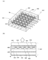
【解決手段】表示パネルと、表示パネルの視認側に設けられ、互いに隣り合う第1の液晶素子及び第2の液晶素子を含むシャッターパネルと、を有し、第1の表示状態においては、第1の液晶素子によって、シャッターパネルに第1の遮光領域と、第1の透光領域と、を形成し、表示パネルからの光は、第1の透光領域から放出され、第2の表示状態においては、第1の液晶素子及び第2の液晶素子によって、シャッターパネルに第1の遮光領域よりも大きい第2の遮光領域と、第1の透光領域よりも小さい第2の透光領域と、を形成し、表示パネルからの光は、第2の透光領域から放出される表示装置である。
【選択図】図1
Description
まず、本発明の一態様の表示装置について図1乃至3を参照して説明する。
本実施の形態では、本発明の一態様の表示装置におけるシャッターパネルの具体例について図4及び図5を用いて説明する。本実施の形態で示すシャッターパネルは、実施の形態1におけるシャッターパネル20の具体例である。
本実施の形態では、実施の形態1で示した表示パネルに適用可能な表示パネルの構成例について図6及び図7を用いて説明する。
本発明の一態様の表示装置は、タッチパネルと呼ばれる位置入力装置を有していてもよい。本実施の形態では、本発明の一態様の表示装置に適用可能なシャッターパネルであって、タッチパネルを具備するシャッターパネルの構成例を、図8を用いて説明する。
本発明の一態様に係る表示装置は、ノート型パーソナルコンピュータ、記録媒体を備えた画像再生装置(代表的にはDVD:Digital Versatile Disc等の記録媒体を再生し、その画像を表示しうるディスプレイを有する装置)に用いることができる。その他に、本発明の一態様に係る表示装置を用いることができる電子機器として、携帯電話、携帯型ゲーム機、携帯情報端末、電子書籍、ビデオカメラ、デジタルスチルカメラ、ゴーグル型ディスプレイ(ヘッドマウントディスプレイ)、ナビゲーションシステム、音響再生装置(カーオーディオ、デジタルオーディオプレイヤー等)、複写機、ファクシミリ、プリンター、プリンター複合機、現金自動預け入れ払い機(ATM)、自動販売機などが挙げられる。本実施の形態においては、これら電子機器の具体例について図9を参照して説明する。
20 シャッターパネル
31 左目
32 右目
100 画素
200 光学シャッタ領域
300 表示装置
301 視認者
302 表示部
303 距離センサ
304 角度センサ
311 表示パネル
312 シャッターパネル
313 アプリケーションプロセッサ
314 表示パネル制御回路
315 シャッターパネル制御回路
316 センサ制御回路
401 ソース側駆動回路
402 画素部
403 ゲート側駆動回路
404 封止基板
405 シール材
407 空間
408 配線
409 FPC(フレキシブルプリントサーキット)
410 素子基板
411 絶縁膜
414 絶縁物
419 絶縁膜
423 nチャネル型トランジスタ
424 pチャネル型トランジスタ
431 EL層
433 電極
501 基板
502 基板
503 液晶
505 電極
506 電極
523 配線
524 容量配線
525 配線
526 配線
601 基板
602 画素部
603 信号線駆動回路
604 走査線駆動回路
605 シール材
606 基板
608 液晶層
610 トランジスタ
611 トランジスタ
613 液晶素子
615 接続端子電極
616 端子電極
618 FPC
619 異方性導電膜
630 電極層
631 電極層
632 絶縁膜
635 スペーサ
640 シャッターパネル
642 偏光板
644 基板
646 基板
648 偏光板
650 液晶素子ユニット
652 基板
660 タッチパネルユニット
661 導電膜
662 第1電極
663 導電膜
664 第2電極
666 絶縁層
668 絶縁層
100a 画素
100b 画素
200A 第1の液晶素子
200B 第2の液晶素子
412a トランジスタ
413a 電極
415a 導電層
418a 発光素子
420a 画素
420b 画素
420c 画素
434a カラーフィルタ層
434b カラーフィルタ層
434c カラーフィルタ層
5001 筐体
5002 筐体
5003 表示部
5004 表示部
5005 マイクロホン
5006 スピーカー
5007 操作キー
5008 スタイラス
5201 筐体
5202 表示部
5203 キーボード
5204 ポインティングデバイス
5401 筐体
5402 表示部
5403 操作キー
500a シャッターパネル
505a 電極
505a1 電極
506a 電極
506a1 電極
506a2 電極
507a1 液晶素子
507a2 液晶素子
516a1 電極
516a2 電極
516a3 電極
520a1 トランジスタ
520a2 トランジスタ
520a3 トランジスタ
521a 配線
522a1 配線
Claims (4)
- 表示パネルと、
前記表示パネルの視認側に設けられ、第1の液晶素子及び前記第1の液晶素子と隣り合う第2の液晶素子を含むシャッターパネルと、を有し、
第1の表示状態においては、前記第1の液晶素子によって、前記シャッターパネルに第1の遮光領域と、第1の透光領域と、を形成し、
前記表示パネルからの光は、前記第1の透光領域から放出され、
第2の表示状態においては、前記第1の液晶素子及び前記第2の液晶素子によって、前記シャッターパネルに前記第1の遮光領域よりも大きい第2の遮光領域と、前記第1の透光領域よりも小さい第2の透光領域と、を形成し、
前記表示パネルからの光は、前記第2の透光領域から放出される表示装置。 - 表示パネルと、
前記表示パネルの視認側に設けられ、第1の液晶素子及び前記第1の液晶素子と隣り合う第2の液晶素子を含むシャッターパネルと、
前記シャッターパネルと視認者との距離及び角度を検出するセンサと、を有し、
第1の表示状態においては、前記第1の液晶素子によって、前記シャッターパネルに第1の遮光領域と、第1の透光領域と、を形成し、
前記表示パネルからの光は、前記第1の透光領域から放出され、
第2の表示状態においては、前記第1の液晶素子及び前記第2の液晶素子によって、前記シャッターパネルに前記第1の遮光領域よりも大きい第2の遮光領域と、前記第1の透光領域よりも小さい第2の透光領域と、を形成し、
前記表示パネルからの光は、前記第2の透光領域から放出され、
前記センサによって検出した距離及び角度に応じて、前記第1の表示状態または前記第2の表示状態を選択する表示装置。 - 請求項1または請求項2において、
前記第1の液晶素子の両側に前記第2の液晶素子が配置された表示装置。 - 請求項1乃至請求項3のいずれか一において、
前記表示パネルは、互いに隣り合う第1の画素及び第2の画素を含む画素ユニットを有し、
前記第1の遮光領域のピッチは、前記画素ユニットのピッチよりも広い表示装置。
Priority Applications (1)
| Application Number | Priority Date | Filing Date | Title |
|---|---|---|---|
| JP2012025709A JP5893424B2 (ja) | 2011-02-16 | 2012-02-09 | 表示装置 |
Applications Claiming Priority (3)
| Application Number | Priority Date | Filing Date | Title |
|---|---|---|---|
| JP2011031103 | 2011-02-16 | ||
| JP2011031103 | 2011-02-16 | ||
| JP2012025709A JP5893424B2 (ja) | 2011-02-16 | 2012-02-09 | 表示装置 |
Related Child Applications (1)
| Application Number | Title | Priority Date | Filing Date |
|---|---|---|---|
| JP2016031795A Division JP6181788B2 (ja) | 2011-02-16 | 2016-02-23 | 液晶表示装置、表示モジュール及び電子機器 |
Publications (3)
| Publication Number | Publication Date |
|---|---|
| JP2012185486A true JP2012185486A (ja) | 2012-09-27 |
| JP2012185486A5 JP2012185486A5 (ja) | 2015-03-19 |
| JP5893424B2 JP5893424B2 (ja) | 2016-03-23 |
Family
ID=46636488
Family Applications (2)
| Application Number | Title | Priority Date | Filing Date |
|---|---|---|---|
| JP2012025709A Expired - Fee Related JP5893424B2 (ja) | 2011-02-16 | 2012-02-09 | 表示装置 |
| JP2016031795A Active JP6181788B2 (ja) | 2011-02-16 | 2016-02-23 | 液晶表示装置、表示モジュール及び電子機器 |
Family Applications After (1)
| Application Number | Title | Priority Date | Filing Date |
|---|---|---|---|
| JP2016031795A Active JP6181788B2 (ja) | 2011-02-16 | 2016-02-23 | 液晶表示装置、表示モジュール及び電子機器 |
Country Status (5)
| Country | Link |
|---|---|
| US (1) | US9035859B2 (ja) |
| JP (2) | JP5893424B2 (ja) |
| KR (1) | KR101899178B1 (ja) |
| TW (2) | TWI579592B (ja) |
| WO (1) | WO2012111427A1 (ja) |
Families Citing this family (13)
| Publication number | Priority date | Publication date | Assignee | Title |
|---|---|---|---|---|
| US9167234B2 (en) | 2011-02-14 | 2015-10-20 | Semiconductor Energy Laboratory Co., Ltd. | Display device |
| US9035860B2 (en) | 2011-02-16 | 2015-05-19 | Semiconductor Energy Laboratory Co., Ltd. | Display device |
| US9443455B2 (en) | 2011-02-25 | 2016-09-13 | Semiconductor Energy Laboratory Co., Ltd. | Display device having a plurality of pixels |
| US8988411B2 (en) | 2011-07-08 | 2015-03-24 | Semiconductor Energy Laboratory Co., Ltd. | Display device |
| TWI504933B (zh) * | 2012-06-13 | 2015-10-21 | Innolux Corp | 可切換式二維/三維顯示裝置及其製造方法 |
| JP6196568B2 (ja) * | 2013-03-27 | 2017-09-13 | ソニーセミコンダクタソリューションズ株式会社 | 表示装置 |
| TWI637348B (zh) * | 2013-04-11 | 2018-10-01 | 緯創資通股份有限公司 | 影像顯示裝置和影像顯示方法 |
| US9455281B2 (en) * | 2014-06-19 | 2016-09-27 | Semiconductor Energy Laboratory Co., Ltd. | Touch sensor, touch panel, touch panel module, and display device |
| CN106886107B (zh) | 2015-12-15 | 2020-02-14 | 群创光电股份有限公司 | 显示面板 |
| KR101800965B1 (ko) * | 2016-06-30 | 2017-11-24 | 엘지디스플레이 주식회사 | 무안경 입체 영상 표시장치 |
| US10477192B2 (en) | 2016-09-14 | 2019-11-12 | Semiconductor Energy Laboratory Co., Ltd. | Display system and electronic device |
| CN108469682A (zh) * | 2018-03-30 | 2018-08-31 | 京东方科技集团股份有限公司 | 一种三维显示装置及其三维显示方法 |
| US10871384B2 (en) * | 2019-02-26 | 2020-12-22 | Thomas P. Moyer | Apparatus and methods utilizing emissive patterns to determine positional information |
Citations (7)
| Publication number | Priority date | Publication date | Assignee | Title |
|---|---|---|---|---|
| JPH10174127A (ja) * | 1996-12-13 | 1998-06-26 | Sanyo Electric Co Ltd | 立体表示方法および立体表示装置 |
| JPH1185085A (ja) * | 1997-09-02 | 1999-03-30 | Fujitsu Ltd | 画像表示装置 |
| JP2001166259A (ja) * | 1999-09-24 | 2001-06-22 | Sanyo Electric Co Ltd | 眼鏡無し立体映像表示装置 |
| JP2005092103A (ja) * | 2003-09-19 | 2005-04-07 | Sharp Corp | 立体映像表示装置 |
| JP2005164916A (ja) * | 2003-12-02 | 2005-06-23 | Canon Inc | 立体表示装置 |
| JP2005172925A (ja) * | 2003-12-08 | 2005-06-30 | Canon Inc | 立体画像表示装置及び方法 |
| JP2009520231A (ja) * | 2005-12-20 | 2009-05-21 | コーニンクレッカ フィリップス エレクトロニクス エヌ ヴィ | 自動立体視表示装置 |
Family Cites Families (34)
| Publication number | Priority date | Publication date | Assignee | Title |
|---|---|---|---|---|
| JP2857429B2 (ja) | 1989-10-02 | 1999-02-17 | 日本放送協会 | 3次元画像表示装置および方法 |
| JP2919759B2 (ja) | 1994-05-18 | 1999-07-19 | 三洋電機株式会社 | 光学フィルタ及びこれを用いる立体表示装置 |
| EP0997868B1 (en) | 1998-10-30 | 2012-03-14 | Semiconductor Energy Laboratory Co., Ltd. | Field sequential liquid crystal display device and driving method thereof, and head mounted display |
| US6597348B1 (en) | 1998-12-28 | 2003-07-22 | Semiconductor Energy Laboratory Co., Ltd. | Information-processing device |
| US7145536B1 (en) | 1999-03-26 | 2006-12-05 | Semiconductor Energy Laboratory Co., Ltd. | Liquid crystal display device |
| EP1087627A3 (en) * | 1999-09-24 | 2004-02-18 | SANYO ELECTRIC Co., Ltd. | Autostereoscopic image display device |
| US6882012B2 (en) | 2000-02-28 | 2005-04-19 | Semiconductor Energy Laboratory Co., Ltd. | Semiconductor device and a method of manufacturing the same |
| TW518552B (en) | 2000-08-18 | 2003-01-21 | Semiconductor Energy Lab | Liquid crystal display device, method of driving the same, and method of driving a portable information device having the liquid crystal display device |
| US7385579B2 (en) | 2000-09-29 | 2008-06-10 | Semiconductor Energy Laboratory Co., Ltd. | Liquid crystal display device and method of driving the same |
| JP2003259395A (ja) | 2002-03-06 | 2003-09-12 | Matsushita Electric Ind Co Ltd | 立体表示方法及び立体表示装置 |
| JP2004077567A (ja) | 2002-08-09 | 2004-03-11 | Semiconductor Energy Lab Co Ltd | 表示装置及びその駆動方法 |
| JP2004094058A (ja) | 2002-09-02 | 2004-03-25 | Semiconductor Energy Lab Co Ltd | 液晶表示装置および液晶表示装置の駆動方法 |
| US7193593B2 (en) | 2002-09-02 | 2007-03-20 | Semiconductor Energy Laboratory Co., Ltd. | Liquid crystal display device and method of driving a liquid crystal display device |
| JP4436120B2 (ja) * | 2002-12-18 | 2010-03-24 | シャープ株式会社 | 液晶表示装置及びその製造方法 |
| US8319219B2 (en) | 2003-07-14 | 2012-11-27 | Semiconductor Energy Laboratory Co., Ltd. | Light-emitting device |
| JP2005258013A (ja) | 2004-03-11 | 2005-09-22 | Sharp Corp | 表示パネルおよび表示装置 |
| CN101714323B (zh) | 2004-04-22 | 2012-12-05 | 株式会社半导体能源研究所 | 发光装置及其驱动方法 |
| US8068200B2 (en) * | 2004-12-24 | 2011-11-29 | Casio Computer Co., Ltd. | Vertical alignment liquid crystal display device in which a pixel electrode has slits which divide the pixel electrode into electrode portions |
| US7826018B2 (en) * | 2004-12-27 | 2010-11-02 | Samsung Electronics Co., Ltd. | Liquid crystal display |
| JP4934974B2 (ja) | 2005-03-17 | 2012-05-23 | エプソンイメージングデバイス株式会社 | 画像表示装置 |
| KR101112735B1 (ko) * | 2005-04-08 | 2012-03-13 | 삼성전자주식회사 | 하이브리드 위치 추적 시스템을 이용한 입체 디스플레이장치 |
| US8106865B2 (en) | 2006-06-02 | 2012-01-31 | Semiconductor Energy Laboratory Co., Ltd. | Display device and driving method thereof |
| US8154493B2 (en) | 2006-06-02 | 2012-04-10 | Semiconductor Energy Laboratory Co., Ltd. | Liquid crystal display device, driving method of the same, and electronic device using the same |
| KR101323736B1 (ko) * | 2007-02-07 | 2013-10-30 | 삼성전자주식회사 | 2차원 겸용 3차원 영상 디스플레이 장치 |
| TWI464510B (zh) * | 2007-07-20 | 2014-12-11 | Semiconductor Energy Lab | 液晶顯示裝置 |
| EP2291856A4 (en) | 2008-06-27 | 2015-09-23 | Semiconductor Energy Lab | THIN FILM TRANSISTOR |
| KR20100036462A (ko) * | 2008-09-30 | 2010-04-08 | 삼성전자주식회사 | 2차원과 3차원 겸용 영상 표시 장치 및 방법 |
| JP5590868B2 (ja) | 2008-12-11 | 2014-09-17 | 株式会社半導体エネルギー研究所 | 半導体装置 |
| JP5100670B2 (ja) | 2009-01-21 | 2012-12-19 | 株式会社半導体エネルギー研究所 | タッチパネル、電子機器 |
| JP5356952B2 (ja) * | 2009-08-31 | 2013-12-04 | レムセン イノベーション、リミティッド ライアビリティー カンパニー | 表示装置 |
| US20110157322A1 (en) | 2009-12-31 | 2011-06-30 | Broadcom Corporation | Controlling a pixel array to support an adaptable light manipulator |
| US9035860B2 (en) * | 2011-02-16 | 2015-05-19 | Semiconductor Energy Laboratory Co., Ltd. | Display device |
| US9443455B2 (en) * | 2011-02-25 | 2016-09-13 | Semiconductor Energy Laboratory Co., Ltd. | Display device having a plurality of pixels |
| JP5917277B2 (ja) * | 2011-05-12 | 2016-05-11 | 株式会社半導体エネルギー研究所 | 表示装置及びその駆動方法 |
-
2012
- 2012-01-25 WO PCT/JP2012/052193 patent/WO2012111427A1/en active Application Filing
- 2012-01-25 KR KR1020137023782A patent/KR101899178B1/ko active IP Right Grant
- 2012-02-07 US US13/367,711 patent/US9035859B2/en not_active Expired - Fee Related
- 2012-02-09 JP JP2012025709A patent/JP5893424B2/ja not_active Expired - Fee Related
- 2012-02-14 TW TW101104727A patent/TWI579592B/zh not_active IP Right Cessation
- 2012-02-14 TW TW106100482A patent/TWI633339B/zh not_active IP Right Cessation
-
2016
- 2016-02-23 JP JP2016031795A patent/JP6181788B2/ja active Active
Patent Citations (7)
| Publication number | Priority date | Publication date | Assignee | Title |
|---|---|---|---|---|
| JPH10174127A (ja) * | 1996-12-13 | 1998-06-26 | Sanyo Electric Co Ltd | 立体表示方法および立体表示装置 |
| JPH1185085A (ja) * | 1997-09-02 | 1999-03-30 | Fujitsu Ltd | 画像表示装置 |
| JP2001166259A (ja) * | 1999-09-24 | 2001-06-22 | Sanyo Electric Co Ltd | 眼鏡無し立体映像表示装置 |
| JP2005092103A (ja) * | 2003-09-19 | 2005-04-07 | Sharp Corp | 立体映像表示装置 |
| JP2005164916A (ja) * | 2003-12-02 | 2005-06-23 | Canon Inc | 立体表示装置 |
| JP2005172925A (ja) * | 2003-12-08 | 2005-06-30 | Canon Inc | 立体画像表示装置及び方法 |
| JP2009520231A (ja) * | 2005-12-20 | 2009-05-21 | コーニンクレッカ フィリップス エレクトロニクス エヌ ヴィ | 自動立体視表示装置 |
Also Published As
| Publication number | Publication date |
|---|---|
| KR101899178B1 (ko) | 2018-09-14 |
| KR20140051151A (ko) | 2014-04-30 |
| JP5893424B2 (ja) | 2016-03-23 |
| TWI579592B (zh) | 2017-04-21 |
| WO2012111427A1 (en) | 2012-08-23 |
| JP2016095539A (ja) | 2016-05-26 |
| TW201239402A (en) | 2012-10-01 |
| TWI633339B (zh) | 2018-08-21 |
| US20120206325A1 (en) | 2012-08-16 |
| JP6181788B2 (ja) | 2017-08-16 |
| US9035859B2 (en) | 2015-05-19 |
| TW201730630A (zh) | 2017-09-01 |
Similar Documents
| Publication | Publication Date | Title |
|---|---|---|
| JP6181788B2 (ja) | 液晶表示装置、表示モジュール及び電子機器 | |
| JP6295293B2 (ja) | 表示装置 | |
| JP5912680B2 (ja) | 表示装置および表示装置の駆動方法 | |
| JP6053293B2 (ja) | 表示装置 | |
| US10817105B2 (en) | Liquid crystal display device | |
| JP6252689B1 (ja) | 表示装置 | |
| JP2017072826A (ja) | 液晶表示装置の駆動方法 | |
| CN103529587B (zh) | 图案化延迟器型立体图像显示设备 | |
| JP2011209346A (ja) | 表示装置及びその駆動制御方法並びに電子機器 | |
| US11429000B2 (en) | Electro-optical device and electronic apparatus | |
| KR102366771B1 (ko) | 액정 표시 장치 |
Legal Events
| Date | Code | Title | Description |
|---|---|---|---|
| A521 | Request for written amendment filed |
Free format text: JAPANESE INTERMEDIATE CODE: A523 Effective date: 20150202 |
|
| A621 | Written request for application examination |
Free format text: JAPANESE INTERMEDIATE CODE: A621 Effective date: 20150202 |
|
| A977 | Report on retrieval |
Free format text: JAPANESE INTERMEDIATE CODE: A971007 Effective date: 20151015 |
|
| A131 | Notification of reasons for refusal |
Free format text: JAPANESE INTERMEDIATE CODE: A131 Effective date: 20151020 |
|
| A521 | Request for written amendment filed |
Free format text: JAPANESE INTERMEDIATE CODE: A523 Effective date: 20151023 |
|
| A131 | Notification of reasons for refusal |
Free format text: JAPANESE INTERMEDIATE CODE: A131 Effective date: 20151208 |
|
| A521 | Request for written amendment filed |
Free format text: JAPANESE INTERMEDIATE CODE: A523 Effective date: 20151214 |
|
| TRDD | Decision of grant or rejection written | ||
| A01 | Written decision to grant a patent or to grant a registration (utility model) |
Free format text: JAPANESE INTERMEDIATE CODE: A01 Effective date: 20160209 |
|
| A61 | First payment of annual fees (during grant procedure) |
Free format text: JAPANESE INTERMEDIATE CODE: A61 Effective date: 20160224 |
|
| R150 | Certificate of patent or registration of utility model |
Ref document number: 5893424 Country of ref document: JP Free format text: JAPANESE INTERMEDIATE CODE: R150 |
|
| R250 | Receipt of annual fees |
Free format text: JAPANESE INTERMEDIATE CODE: R250 |
|
| R250 | Receipt of annual fees |
Free format text: JAPANESE INTERMEDIATE CODE: R250 |
|
| R250 | Receipt of annual fees |
Free format text: JAPANESE INTERMEDIATE CODE: R250 |
|
| R250 | Receipt of annual fees |
Free format text: JAPANESE INTERMEDIATE CODE: R250 |
|
| LAPS | Cancellation because of no payment of annual fees |