US7826018B2 - Liquid crystal display - Google Patents

Liquid crystal display Download PDF

Info

Publication number
US7826018B2
US7826018B2 US11/319,074 US31907405A US7826018B2 US 7826018 B2 US7826018 B2 US 7826018B2 US 31907405 A US31907405 A US 31907405A US 7826018 B2 US7826018 B2 US 7826018B2
Authority
US
United States
Prior art keywords
electrode
liquid crystal
subpixel
crystal display
electrodes
Prior art date
Legal status (The legal status is an assumption and is not a legal conclusion. Google has not performed a legal analysis and makes no representation as to the accuracy of the status listed.)
Expired - Fee Related, expires
Application number
US11/319,074
Other versions
US20060146242A1 (en
Inventor
Dong-Gyu Kim
Sahng-Ik Jun
Sung-Jae Moon
Current Assignee (The listed assignees may be inaccurate. Google has not performed a legal analysis and makes no representation or warranty as to the accuracy of the list.)
Samsung Display Co Ltd
Original Assignee
Samsung Electronics Co Ltd
Priority date (The priority date is an assumption and is not a legal conclusion. Google has not performed a legal analysis and makes no representation as to the accuracy of the date listed.)
Filing date
Publication date
Priority claimed from KR1020040113308A external-priority patent/KR101337265B1/en
Priority claimed from KR1020050083267A external-priority patent/KR101240646B1/en
Application filed by Samsung Electronics Co Ltd filed Critical Samsung Electronics Co Ltd
Assigned to SAMSUNG ELECTRONICS CO., LTD. reassignment SAMSUNG ELECTRONICS CO., LTD. ASSIGNMENT OF ASSIGNORS INTEREST (SEE DOCUMENT FOR DETAILS). Assignors: JUN, SAHNG-IK, KIM, DONG-GYU, MOON, SUNG-JAE
Publication of US20060146242A1 publication Critical patent/US20060146242A1/en
Application granted granted Critical
Publication of US7826018B2 publication Critical patent/US7826018B2/en
Assigned to SAMSUNG DISPLAY CO., LTD. reassignment SAMSUNG DISPLAY CO., LTD. ASSIGNMENT OF ASSIGNORS INTEREST (SEE DOCUMENT FOR DETAILS). Assignors: SAMSUNG ELECTRONICS CO., LTD.
Expired - Fee Related legal-status Critical Current
Adjusted expiration legal-status Critical

Links

Images

Classifications

    • GPHYSICS
    • G02OPTICS
    • G02FOPTICAL DEVICES OR ARRANGEMENTS FOR THE CONTROL OF LIGHT BY MODIFICATION OF THE OPTICAL PROPERTIES OF THE MEDIA OF THE ELEMENTS INVOLVED THEREIN; NON-LINEAR OPTICS; FREQUENCY-CHANGING OF LIGHT; OPTICAL LOGIC ELEMENTS; OPTICAL ANALOGUE/DIGITAL CONVERTERS
    • G02F1/00Devices or arrangements for the control of the intensity, colour, phase, polarisation or direction of light arriving from an independent light source, e.g. switching, gating or modulating; Non-linear optics
    • G02F1/01Devices or arrangements for the control of the intensity, colour, phase, polarisation or direction of light arriving from an independent light source, e.g. switching, gating or modulating; Non-linear optics for the control of the intensity, phase, polarisation or colour 
    • G02F1/13Devices or arrangements for the control of the intensity, colour, phase, polarisation or direction of light arriving from an independent light source, e.g. switching, gating or modulating; Non-linear optics for the control of the intensity, phase, polarisation or colour  based on liquid crystals, e.g. single liquid crystal display cells
    • G02F1/137Devices or arrangements for the control of the intensity, colour, phase, polarisation or direction of light arriving from an independent light source, e.g. switching, gating or modulating; Non-linear optics for the control of the intensity, phase, polarisation or colour  based on liquid crystals, e.g. single liquid crystal display cells characterised by the electro-optical or magneto-optical effect, e.g. field-induced phase transition, orientation effect, guest-host interaction or dynamic scattering
    • G02F1/139Devices or arrangements for the control of the intensity, colour, phase, polarisation or direction of light arriving from an independent light source, e.g. switching, gating or modulating; Non-linear optics for the control of the intensity, phase, polarisation or colour  based on liquid crystals, e.g. single liquid crystal display cells characterised by the electro-optical or magneto-optical effect, e.g. field-induced phase transition, orientation effect, guest-host interaction or dynamic scattering based on orientation effects in which the liquid crystal remains transparent
    • G02F1/1393Devices or arrangements for the control of the intensity, colour, phase, polarisation or direction of light arriving from an independent light source, e.g. switching, gating or modulating; Non-linear optics for the control of the intensity, phase, polarisation or colour  based on liquid crystals, e.g. single liquid crystal display cells characterised by the electro-optical or magneto-optical effect, e.g. field-induced phase transition, orientation effect, guest-host interaction or dynamic scattering based on orientation effects in which the liquid crystal remains transparent the birefringence of the liquid crystal being electrically controlled, e.g. ECB-, DAP-, HAN-, PI-LC cells
    • GPHYSICS
    • G02OPTICS
    • G02FOPTICAL DEVICES OR ARRANGEMENTS FOR THE CONTROL OF LIGHT BY MODIFICATION OF THE OPTICAL PROPERTIES OF THE MEDIA OF THE ELEMENTS INVOLVED THEREIN; NON-LINEAR OPTICS; FREQUENCY-CHANGING OF LIGHT; OPTICAL LOGIC ELEMENTS; OPTICAL ANALOGUE/DIGITAL CONVERTERS
    • G02F1/00Devices or arrangements for the control of the intensity, colour, phase, polarisation or direction of light arriving from an independent light source, e.g. switching, gating or modulating; Non-linear optics
    • G02F1/01Devices or arrangements for the control of the intensity, colour, phase, polarisation or direction of light arriving from an independent light source, e.g. switching, gating or modulating; Non-linear optics for the control of the intensity, phase, polarisation or colour 
    • G02F1/13Devices or arrangements for the control of the intensity, colour, phase, polarisation or direction of light arriving from an independent light source, e.g. switching, gating or modulating; Non-linear optics for the control of the intensity, phase, polarisation or colour  based on liquid crystals, e.g. single liquid crystal display cells
    • G02F1/133Constructional arrangements; Operation of liquid crystal cells; Circuit arrangements
    • G02F1/1333Constructional arrangements; Manufacturing methods
    • G02F1/1343Electrodes
    • G02F1/134309Electrodes characterised by their geometrical arrangement
    • G02F1/134336Matrix
    • GPHYSICS
    • G02OPTICS
    • G02FOPTICAL DEVICES OR ARRANGEMENTS FOR THE CONTROL OF LIGHT BY MODIFICATION OF THE OPTICAL PROPERTIES OF THE MEDIA OF THE ELEMENTS INVOLVED THEREIN; NON-LINEAR OPTICS; FREQUENCY-CHANGING OF LIGHT; OPTICAL LOGIC ELEMENTS; OPTICAL ANALOGUE/DIGITAL CONVERTERS
    • G02F1/00Devices or arrangements for the control of the intensity, colour, phase, polarisation or direction of light arriving from an independent light source, e.g. switching, gating or modulating; Non-linear optics
    • G02F1/01Devices or arrangements for the control of the intensity, colour, phase, polarisation or direction of light arriving from an independent light source, e.g. switching, gating or modulating; Non-linear optics for the control of the intensity, phase, polarisation or colour 
    • G02F1/13Devices or arrangements for the control of the intensity, colour, phase, polarisation or direction of light arriving from an independent light source, e.g. switching, gating or modulating; Non-linear optics for the control of the intensity, phase, polarisation or colour  based on liquid crystals, e.g. single liquid crystal display cells
    • G02F1/133Constructional arrangements; Operation of liquid crystal cells; Circuit arrangements
    • G02F1/1333Constructional arrangements; Manufacturing methods
    • G02F1/1337Surface-induced orientation of the liquid crystal molecules, e.g. by alignment layers
    • G02F1/133707Structures for producing distorted electric fields, e.g. bumps, protrusions, recesses, slits in pixel electrodes
    • GPHYSICS
    • G02OPTICS
    • G02FOPTICAL DEVICES OR ARRANGEMENTS FOR THE CONTROL OF LIGHT BY MODIFICATION OF THE OPTICAL PROPERTIES OF THE MEDIA OF THE ELEMENTS INVOLVED THEREIN; NON-LINEAR OPTICS; FREQUENCY-CHANGING OF LIGHT; OPTICAL LOGIC ELEMENTS; OPTICAL ANALOGUE/DIGITAL CONVERTERS
    • G02F1/00Devices or arrangements for the control of the intensity, colour, phase, polarisation or direction of light arriving from an independent light source, e.g. switching, gating or modulating; Non-linear optics
    • G02F1/01Devices or arrangements for the control of the intensity, colour, phase, polarisation or direction of light arriving from an independent light source, e.g. switching, gating or modulating; Non-linear optics for the control of the intensity, phase, polarisation or colour 
    • G02F1/13Devices or arrangements for the control of the intensity, colour, phase, polarisation or direction of light arriving from an independent light source, e.g. switching, gating or modulating; Non-linear optics for the control of the intensity, phase, polarisation or colour  based on liquid crystals, e.g. single liquid crystal display cells
    • G02F1/133Constructional arrangements; Operation of liquid crystal cells; Circuit arrangements
    • G02F1/1333Constructional arrangements; Manufacturing methods
    • G02F1/1343Electrodes
    • G02F1/134309Electrodes characterised by their geometrical arrangement
    • G02F1/134345Subdivided pixels, e.g. for grey scale or redundancy
    • GPHYSICS
    • G02OPTICS
    • G02FOPTICAL DEVICES OR ARRANGEMENTS FOR THE CONTROL OF LIGHT BY MODIFICATION OF THE OPTICAL PROPERTIES OF THE MEDIA OF THE ELEMENTS INVOLVED THEREIN; NON-LINEAR OPTICS; FREQUENCY-CHANGING OF LIGHT; OPTICAL LOGIC ELEMENTS; OPTICAL ANALOGUE/DIGITAL CONVERTERS
    • G02F1/00Devices or arrangements for the control of the intensity, colour, phase, polarisation or direction of light arriving from an independent light source, e.g. switching, gating or modulating; Non-linear optics
    • G02F1/01Devices or arrangements for the control of the intensity, colour, phase, polarisation or direction of light arriving from an independent light source, e.g. switching, gating or modulating; Non-linear optics for the control of the intensity, phase, polarisation or colour 
    • G02F1/13Devices or arrangements for the control of the intensity, colour, phase, polarisation or direction of light arriving from an independent light source, e.g. switching, gating or modulating; Non-linear optics for the control of the intensity, phase, polarisation or colour  based on liquid crystals, e.g. single liquid crystal display cells
    • G02F1/133Constructional arrangements; Operation of liquid crystal cells; Circuit arrangements
    • G02F1/136Liquid crystal cells structurally associated with a semi-conducting layer or substrate, e.g. cells forming part of an integrated circuit
    • G02F1/1362Active matrix addressed cells
    • G02F1/136213Storage capacitors associated with the pixel electrode
    • GPHYSICS
    • G02OPTICS
    • G02FOPTICAL DEVICES OR ARRANGEMENTS FOR THE CONTROL OF LIGHT BY MODIFICATION OF THE OPTICAL PROPERTIES OF THE MEDIA OF THE ELEMENTS INVOLVED THEREIN; NON-LINEAR OPTICS; FREQUENCY-CHANGING OF LIGHT; OPTICAL LOGIC ELEMENTS; OPTICAL ANALOGUE/DIGITAL CONVERTERS
    • G02F1/00Devices or arrangements for the control of the intensity, colour, phase, polarisation or direction of light arriving from an independent light source, e.g. switching, gating or modulating; Non-linear optics
    • G02F1/01Devices or arrangements for the control of the intensity, colour, phase, polarisation or direction of light arriving from an independent light source, e.g. switching, gating or modulating; Non-linear optics for the control of the intensity, phase, polarisation or colour 
    • G02F1/13Devices or arrangements for the control of the intensity, colour, phase, polarisation or direction of light arriving from an independent light source, e.g. switching, gating or modulating; Non-linear optics for the control of the intensity, phase, polarisation or colour  based on liquid crystals, e.g. single liquid crystal display cells
    • G02F1/133Constructional arrangements; Operation of liquid crystal cells; Circuit arrangements
    • G02F1/136Liquid crystal cells structurally associated with a semi-conducting layer or substrate, e.g. cells forming part of an integrated circuit
    • G02F1/1362Active matrix addressed cells
    • G02F1/13624Active matrix addressed cells having more than one switching element per pixel

Definitions

  • the present invention relates to a liquid crystal display.
  • a liquid crystal display is one of the most widely used flat panel display devices.
  • the LCD includes a pair of panels (e.g., a lower panel and an upper panel) including pixel electrodes, a common electrode and a liquid crystal (LC) layer interposed between the panels.
  • the LC layer has dielectric anisotropy.
  • the LCD generates an electric field in the LC layer by applying voltages to the electrodes, and obtains desired images by controlling the strength of the electric field via the applied voltages to vary the transmittance of light incident on the LC layer.
  • the LCD further includes switching elements connected to the pixel electrodes and signal lines, such as gate lines and data lines, for applying signals to the switching elements, thereby applying voltages to the pixel electrodes.
  • VA mode LCD which aligns LC molecules such that the long axes of the LC molecules are perpendicular to the panels in the absence of electric field, is spotlighted because of the high contrast ratio and wide reference viewing angle obtained with the VA mode LCD.
  • the wide viewing angle of the VA mode LCD can be realized by protrusions on and/or cutouts in the field-generating electrodes. Since the cutouts and the protrusions can determine the tilt directions of the LC molecules, the tilt directions can be distributed into several directions by using the cutouts and/or the protrusions such that the reference viewing angle is widened.
  • the VA mode LCD has poor lateral visibility as compared with front visibility.
  • a lateral gamma curve is different from a front gamma curve.
  • a conventional method includes dividing a pixel into two subpixels capacitively coupled to each other. One of the two subpixels is directly supplied with a voltage, while the other is subjected to a voltage drop by the capacitive coupling such that the two subpixels have different voltages, and therefore, cause different transmittances of light incident on the LC layer.
  • the conventional method may not control the transmittances of the two subpixels.
  • the transmittance is varied depending on the color of light, it is preferred that the voltages for different colors are different, however, this may not be possible.
  • the aperture ratio is reduced due to the addition of conductors for capacitive coupling, and the transmittance is reduced due to the voltage drop caused by the capacitive coupling.
  • the polarity of the data voltages relative to a common voltage is inverted every frame, every predetermined number of row or columns, or every pixel for preventing disadvantages including degradation caused by a long-time application of a unidirectional electric field.
  • a column inversion which reverses the polarity of the data lines every predetermined number of pixel columns, keeps the polarity of the data voltages applied to a data line for a predetermined time to reduce the signal delay of the data lines and to reduce the power consumption.
  • the column inversion may cause vertical flickering and vertical crosstalk to degrade the image quality of the LCD.
  • a liquid crystal display includes: a substrate; and a pixel electrode disposed on the substrate and includes a first subpixel electrode and a second subpixel electrode.
  • the first subpixel electrode includes a first electrode including at least two substantially parallelogram shaped electrode pieces that have different inclination directions.
  • the second subpixel electrode includes a second electrode disposed at a longitudinal position different from the first electrode, and includes at least two substantially parallelogram shaped electrode pieces that have different inclination directions.
  • the first electrode and the second electrode may be adjacent to each other.
  • the first electrode and the second electrode may have different heights.
  • the second subpixel electrode may include a third electrode including at least substantially two parallelogram shaped electrode pieces that have different inclination directions, and the third electrode may be transversely adjacent to the first electrode and connected to the second electrode.
  • the first and the second pixel electrodes may be aligned at an edge.
  • the first electrode and the second electrode may be aligned in a diagonal direction relative to one another.
  • the first electrode and the second electrode may be aligned at a center defining a joint between the two substantially parallelogram shaped electrode pieces.
  • the first electrode and the second electrode may have different widths.
  • the height of the first electrode may be greater than the height of the second electrode and equal to or smaller than twice the height of the second electrodes.
  • the first subpixel electrode and the second subpixel electrode may have different areas.
  • the area of the second subpixel electrode may be from about 1.1 times to about three times the area of the first subpixel electrode.
  • the liquid crystal display may further include a common electrode facing the pixel electrode and having a cutout, wherein each of the electrode pieces have a pair of oblique edges substantially parallel to each other, and the cutout passes through the first and the second subpixel electrodes and includes an oblique portion extending substantially parallel to the oblique edges of the electrode pieces.
  • the first subpixel electrode and the second subpixel electrode may have different voltages.
  • the voltages of the first subpixel electrode and the second subpixel electrode may be originated from a single image information.
  • the liquid crystal display may further include: a first thin film transistor coupled to the first subpixel electrode; a second thin film transistor coupled to the second subpixel electrode; first and second signal lines coupled to the first thin film transistor; and third and fourth signal lines coupled to the second thin film transistor.
  • the liquid crystal display may further include: a first thin film transistor coupled to the first subpixel electrode; a second thin film transistor coupled to the second subpixel electrode; a first signal line coupled to the first thin film transistor; a second signal line coupled to the second thin film transistor; and a third signal line coupled to the first and the second thin film transistors and intersecting the first and the second signal lines.
  • the first and the second thin film transistors may be turned on according to signals from the first and the second signal lines, respectively, to transmit signals from the third signal line.
  • the first and the second thin film transistors may be turned on according to a signal from the third signal line, respectively, to transmit signals from the first and the second signal lines.
  • the liquid crystal display may further include a fourth signal line extending along a boundary of the first electrode and the second electrode.
  • the first thin film transistor may include a first drain electrode overlapping the fourth signal line and the second thin film transistor may include a second drain electrode overlapping the fourth signal line.
  • the liquid crystal display may further include: a fourth signal line passing through a center of the first electrode; and a fifth signal line passing through a center of the second electrode, wherein the center is defined by a joint of the two substantially parallelogram shaped electrode pieces.
  • the first thin film transistor may include a first drain electrode overlapping the fourth signal line and the second thin film transistor may include a second drain electrode overlapping the fifth signal line.
  • the first subpixel electrode and the second subpixel electrode may be capacitively coupled to each other.
  • the liquid crystal display may further include a coupling electrode connected to the first subpixel electrode and overlapping the second subpixel electrode.
  • the liquid crystal display may further include: a first thin film transistor coupled to the first subpixel electrode; a second thin film transistor coupled to the second subpixel electrode; a gate line coupled to the first and the second thin film transistors; a data line coupled to the first and the second thin film transistors; a first storage electrode line overlapping the first subpixel electrode; and a second storage electrode line overlapping the second subpixel electrode.
  • a first voltage of the first storage electrode line may have a phase opposite to a phase of a second voltage of the second storage electrode line.
  • the gate line may pass through a boundary between the first subpixel electrode and the second subpixel electrode.
  • the second subpixel electrode may have a cutout.
  • the liquid crystal display may further include: a common electrode facing the pixel electrode; and a liquid crystal layer disposed between the pixel electrode and the common electrode.
  • the common electrode may have a cutout.
  • the liquid crystal display may further include a protrusion formed on the common electrode.
  • a liquid crystal display includes: a substrate; and a plurality of groups of pixel electrodes formed on the substrate.
  • Each of the groups of pixel electrode includes a plurality of pixel electrodes.
  • Each of the pixel electrodes includes a first subpixel electrode and a second subpixel electrode separated from the first subpixel electrode.
  • Each of the first and the second subpixel electrodes includes at least two substantially parallelogram shaped electrode pieces that have different inclination directions, and at least one of the pixel electrodes in each of the groups of pixel electrodes have a different shape from the other pixel electrodes.
  • the groups of the pixel electrodes may be periodically arranged in row and column directions.
  • the pixel electrodes in each of the groups of the pixel electrodes may have an equal area.
  • the pixel electrodes in each of the groups of the pixel electrodes may have different areas.
  • the pixel electrodes in each of the groups of pixel electrodes may be aligned at an edge.
  • An area of the second subpixel electrode may be from about 1.1 times to about three times an area of the first subpixel electrode.
  • the first subpixel electrode and the second subpixel electrode may have different voltages.
  • FIG. 1 is a block diagram of an LCD according to an exemplary embodiment of the present invention
  • FIG. 2 is a schematic equivalent circuit diagram of a pixel of the LCD of FIG. 1 according to an exemplary embodiment of the present invention
  • FIGS. 3-8 are plan view layout diagrams of pixel electrodes and a common electrode in a LC panel assembly according to exemplary embodiments of the present invention.
  • FIGS. 9A-9C are plan views of electrode pieces and a base electrode forming a subpixel electrode shown in FIGS. 3-8 ;
  • FIGS. 10A and 10B are schematic equivalent circuit diagrams of the signal lines and pixels PX′ according to an exemplary embodiment of the present invention.
  • FIG. 11 is a plan view layout of a lower panel (TFT array panel) according to an exemplary embodiment of the present invention.
  • FIG. 12 is a plan view layout of an upper panel (common electrode panel) according to an exemplary embodiment of the present invention.
  • FIG. 13 is a plan view layout of an LC panel assembly including the TFT array panel shown in FIG. 11 and the common electrode panel shown in FIG. 12 ;
  • FIG. 14 is a cross-sectional view of the LC panel assembly shown in FIG. 13 taken along lines XIV-XIV;
  • FIG. 15 is a plan view layout of a TFT array panel according to another exemplary embodiment of the present invention.
  • FIG. 16 is a plan view layout of a common electrode panel according to another exemplary embodiment of the present invention.
  • FIG. 17 is a plan view layout of an LC panel assembly including the TFT array panel shown in FIG. 15 and the common electrode panel shown in FIG. 16 ;
  • FIG. 18 is a cross-sectional view of the LC panel assembly shown in FIG. 17 taken along lines XVIII-XVIII;
  • FIGS. 19 , 21 , 22 , 23 and 24 are plan view layouts of a LC panel assembly according to other exemplary embodiments of the present invention.
  • FIG. 20 is a cross-sectional view of the LC panel assembly shown in FIG. 19 taken along lines XX-XX;
  • FIG. 25 shows a schematic equivalent circuit diagram of the signal lines and a pixel PX according to an exemplary embodiment of the present invention
  • FIG. 26 is a plan view layout of the LC panel assembly of FIG. 25 according to an exemplary embodiment of the present invention.
  • FIG. 27 is a cross-sectional view of the LC panel assembly shown in FIG. 26 taken along lines XXVII-XXVII;
  • FIG. 28 shows a schematic equivalent circuit diagram of the signal lines and a pixel PX according to an exemplary embodiment of the present invention
  • FIGS. 29 , 31 , 32 and 33 are plan view layouts of a LC panel assembly according to exemplary embodiments of the present invention.
  • FIG. 30 is a cross-sectional view of the LC panel assembly shown in FIG. 29 taken along lines XXX-XXX;
  • FIG. 34 shows a schematic equivalent circuit diagram of the signal lines and a pixel PX according to an exemplary embodiment of the present invention.
  • FIGS. 35 , 36 , 37 and 38 are plan view layouts of a LC panel assembly according to exemplary embodiments of the present invention.
  • first, second, third etc. may be used herein to describe various elements, components, regions, layers and/or sections, these elements, components, regions, layers and/or sections should not be limited by these terms. These terms are only used to distinguish one element, component, region, layer or section from another region, layer or section. Thus, a first element, component, region, layer or section discussed below could be termed a second element, component, region, layer or section without departing from the teachings of the present invention.
  • relative terms such as “lower” or “bottom” and “upper” or “top,” may be used herein to describe one element's relationship to another elements as illustrated in the Figures. It will be understood that relative terms are intended to encompass different orientations of the device in addition to the orientation depicted in the Figures. For example, if the device in one of the figures is turned over, elements described as being on the “lower” side of other elements would then be oriented on “upper” sides of the other elements. The exemplary term “lower”, can therefore, encompasses both an orientation of “lower” and “upper,” depending of the particular orientation of the figure.
  • Embodiments of the present invention are described herein with reference to cross section illustrations that are schematic illustrations of idealized embodiments of the present invention. As such, variations from the shapes of the illustrations as a result, for example, of manufacturing techniques and/or tolerances, are to be expected. Thus, embodiments of the present invention should not be construed as limited to the particular shapes of regions illustrated herein but are to include deviations in shapes that result, for example, from manufacturing. For example, a region illustrated or described as flat may, typically, have rough and/or nonlinear features. Moreover, sharp angles that are illustrated may be rounded. Thus, the regions illustrated in the figures are schematic in nature and their shapes are not intended to illustrate the precise shape of a region and are not intended to limit the scope of the present invention.
  • FIG. 1 is a block diagram of an LCD according to an exemplary embodiment of the present invention.
  • FIG. 2 is an equivalent circuit diagram of a pixel of the LCD of FIG. 1 .
  • an LCD includes a LC panel assembly 300 , a gate driver 400 and a data driver 500 that are connected to the panel assembly 300 , a gray voltage generator 800 connected to the data driver 500 and a signal controller 600 controlling the above enumerated elements.
  • the panel assembly 300 includes a plurality of signal lines (not shown) and a plurality of pixels PX connected thereto and arranged substantially in a matrix.
  • the panel assembly 300 includes a lower panel 100 , an upper panel 200 and a LC layer 3 interposed therebetween.
  • the signal lines which are provided on the lower panel 100 , include a plurality of gate lines (not shown) transmitting gate signals (also referred to as “scanning signals”), and a plurality of data lines (not shown) transmitting data signals.
  • the gate lines extend substantially in a row or horizontal direction and substantially parallel to each other, while the data lines extend substantially in a column or vertical direction (e.g., substantially normal to the gate lines and in the same plane) and substantially parallel to each other, relative to the illustrated FIGS. 1 and 2 .
  • each pixel PX includes a pair of subpixels and each subpixel includes a liquid crystal (LC) capacitor (Clc 1 /Clc 2 ). At least one of the two subpixels further includes a switching element (not shown) connected to a gate line, a data line and a LC capacitor Clc 1 /Clc 2 .
  • LC liquid crystal
  • the LC capacitor Clc 1 /Clc 2 includes a subpixel electrode PE 1 /PE 2 and a common electrode CE provided on an upper panel 200 as two terminals.
  • the LC layer 3 disposed between the electrodes PE 1 /PE 2 and common electrode CE functions as a dielectric of the LC capacitor Clc 1 /Clc 2 .
  • the subpixel electrodes PE 1 and PE 2 are separated from each other and form a pixel electrode PE.
  • the common electrode CE is supplied with a common voltage Vcom and covers an entire surface of the upper panel 200 .
  • the LC layer 3 has negative dielectric anisotropy, and LC molecules in the LC layer 3 are defined by long axes that may be oriented perpendicular to the surfaces of the panels 100 and 200 in the absence of an electric field.
  • each pixel PX uniquely represents one of a plurality of primary colors (i.e., spatial division) or each pixel PX sequentially represents the primary colors in turn (i.e., temporal division) such that spatial or temporal sum of the primary colors are recognized as a desired color.
  • An example of a set of the primary colors includes red, green and blue colors.
  • FIG. 2 shows an example of spatial division in that each pixel PX includes a color filter CF representing one of the primary colors in an area of the upper panel 200 facing the pixel electrode PE.
  • the color filter CF is provided on or under the subpixel electrode PE 1 or PE 2 located on the lower panel 100 .
  • a pair of polarizers (not shown) are attached to at least one of the panels 100 and 200 .
  • the polarization axes of the two polarizers may be crossed such that the crossed polarizers block the light incident onto the LC layer 3 . It is will be recognized by those skilled in the pertinent art that one of the polarizers may be omitted.
  • FIGS. 3-8 are plan view layout diagrams of pixel electrodes and a common electrode in a LC panel assembly according to exemplary embodiments of the present invention.
  • FIGS. 9A-9C are planar views of electrode pieces and a base electrode forming a subpixel electrode shown in FIGS. 3-8 .
  • the common electrode CE (shown in FIG. 2 ) has a plurality of protrusions 280 or cutouts 60 U and 60 L ( FIG. 8 ) facing the subpixel electrodes PE 1 , PE 2 , PEij and PE(i+1)j.
  • Both of the subpixel electrodes PE 1 and PE 2 , or PEij and PE(i+1)j forming a pixel electrode PE may be coupled to respective switching elements (not shown).
  • one of the subpixel electrodes PE 1 , PE 2 , PEij and PE(i+1)j may be coupled to a switching element (not shown), while the other of the subpixel electrodes PE 1 , PE 2 , PEij and PE(i+1)j is capacitively coupled to one of the subpixel electrodes PE 1 , PE 2 , PEij and PE(i+1)j.
  • Each of the subpixel electrodes PE 1 , PE 2 , PEij and PE(i+1)j includes at least one electrode piece 196 shown in FIG. 9A and at least one electrode piece 197 shown in FIG. 9B .
  • the electrode pieces 196 and 197 shown in FIGS. 9A and 9B are vertically connected at longitudinal terminal ends thereof to form a base electrode 198 shown in FIG. 9C , which is a basic structure of each of the subpixel electrodes PE 1 , PE 2 , PEij and PE(i+1)j.
  • each of the electrode pieces 196 and 197 has substantially a shape of a parallelogram having a pair of oblique edges 196 o and 197 o and a pair of transverse edges 196 t and 197 t , respectively.
  • Each of the oblique edges 196 o and 197 o makes an oblique angle with the transverse edges 196 t and 197 t , respectively, and the oblique angle ranges from about 45 degrees to about 135 degrees, depending on which pair of parallel oblique edges is compared to a respective transverse edge.
  • the electrode pieces 196 and 197 are classified into two types based on the inclination direction relative to a normal of the bottom edges 196 t and 197 t .
  • the electrode piece 196 shown in FIG. 9A is referred to as “right-inclined” since it is inclined to the right, while the electrode piece 197 shown in FIG. 9B is referred to as “left-inclined” since it is inclined to the left.
  • the width W of the electrode pieces 196 and 197 which is defined as the length of the transverse edges 196 t and 197 t
  • the height H which is defined as the distance between the transverse edges 196 t and 197 t
  • the transverse edges 196 t and 197 t of each of the electrode pieces 196 and 197 may be deformed to be bent or projected in connection with other portions, and the term “parallelogram” used in this specification includes such deformations.
  • the common electrode CE has cutouts 61 and 62 facing the electrode pieces 196 and 197 , and each of the electrode pieces 196 and 197 are partitioned into two sub-areas S 1 and S 2 by the cutouts 61 and 62 .
  • Each of the cutouts 61 and 62 includes an oblique portion 61 o and 62 o substantially parallel to the oblique edges 196 o and 197 o of the electrode pieces 196 and 197 , respectively, and a respective pair of transverse portions 61 t and 62 t , which define an obtuse angle with the oblique portion 61 o and 62 o and overlap the transverse edges 196 t and 197 t of the electrode pieces 196 and 197 .
  • Each of the sub-areas S 1 and S 2 has a pair of primary edges defined by the oblique portion 61 o and 62 o (of the cutouts 61 and 62 , respectively) and the oblique edges 196 o and 197 o (of the electrode pieces 196 and 197 , respectively).
  • the distance between the primary edges, i.e., the width of the sub-areas S 1 and S 2 is preferably equal to about 25 microns to about 40 microns.
  • the base electrode 198 shown in FIG. 9C is formed by combining respective transverse edges of the right-inclined electrode piece 196 and the left-inclined electrode piece 197 .
  • the angle formed by combining the right-inclined electrode piece 196 with the left-inclined electrode piece 197 is preferably equal to about a right angle, and the connection therebetween the electrode pieces 196 and 197 includes connection of only portions of the respective transverse edges 196 t and 197 t .
  • the proximate facing transverse edge portions of the electrode pieces 196 and 197 which are not connected to each other, form a cutout 90 disposed at a concavity. However, when the connection is done at all portions defining the abutting transverse edges 196 t and 197 t of the electrode pieces 196 and 197 , the cutout 90 may not be formed.
  • the outbound or outer transverse edges 196 t and 197 t of the electrode pieces 196 and 197 form transverse edges 198 t of the base electrode 198 .
  • Corresponding oblique edges 196 o and 197 o of the electrode pieces 196 and 197 are connected to each other to form corresponding curved edges 198 o 1 and 198 o 2 of the base electrode 198 .
  • the curved edges 198 o 1 and 198 o 2 includes a convex edge 198 o 1 meeting the opposing transverse edges 198 t at an obtuse angle, for example, about 135 degrees, and a concave edge 198 o 2 meeting the opposing transverse edges 198 t at an acute angle, for example, about 45 degrees.
  • the curved edges 198 o 1 and 198 o 2 each define a substantially 90-degree angle by the meeting of the oblique edges 196 o and 197 o.
  • the cutout 90 extends from a concave vertex CV on the concave edge 198 o 2 toward a convex vertex VV of the convex edge 198 o 1 and reaches near a center of the base electrode 198 defined by the joint between transverse edges 196 t and 197 t.
  • the cutouts 61 and 62 of the common electrode CE are connected to each other to form a cutout 60 .
  • the transverse portions 61 t and 62 t of the cutouts 61 and 62 which overlap each other, are joined together to form a transverse portion 60 t 1 .
  • a newly formed cutout 60 can be described as follows.
  • the cutout 60 includes a curved portion 60 o having a curved point CP, a center transverse portion 60 t 1 connected to the curved point CP of the curved portion 60 o and a pair of terminal transverse portions 60 t 2 connected to ends of the curved portion 60 o .
  • the curved portion 60 o of the cutout 60 includes a pair of oblique portions meeting at the center of the base electrode 198 defining substantially about a right angle.
  • the curved portion 60 o of the cutout 60 extends substantially parallel to the curved edges 198 o 1 and 198 o 2 of the base electrode 198 , and bisects the base electrode 198 into left and right halves.
  • the center transverse portion 60 t 1 of the cutout 60 makes an obtuse angle, for example, about 135 degrees, with the curved portion 60 o , and extends toward the convex vertex VV of the base electrode 198 .
  • the outboard terminal transverse portions 60 t 2 are substantially aligned with the transverse edges 198 t of the base electrode 198 and form an obtuse angle, for example, about 135 degrees, with the curved portion 60 o.
  • the base electrode 198 and the cutout 60 has an inversion symmetry with respect to an imaginary straight line (referred to as a center transverse line) connecting the convex vertex VV and the concave vertex CV of the base electrode 198 .
  • the base electrodes are arranged in two rows.
  • the base electrodes have the same width, but they may have different widths as illustrated in FIGS. 3-8 .
  • the height H 0 of the base electrodes disposed in an upper row is equal to the height H 0 of the base electrodes disposed in a lower row.
  • each row (for a total of six base electrodes) form a basic unit referred to as a dot.
  • Each of subpixel electrodes PE 1 and PE 2 includes one base electrode.
  • Each of the subpixel electrodes PE 11 , PE 21 , PE 12 and PE 22 shown in FIG. 4 includes two adjacent base electrodes in a row, and each of the subpixel electrodes PE 13 and PE 23 includes one base electrode.
  • the connection between the adjacent base electrodes in the row is done at upper and lower corners of the base electrodes, and thus a gap between the base electrodes form a cutout 90 U or 90 L.
  • Each of the subpixel electrodes PE 31 , PE 41 , PE 32 and PE 42 shown in FIG. 7 includes two adjacent base electrodes in a column, and each of the subpixel electrodes PE 33 and PE 43 includes one base electrode.
  • Each of the subpixel electrodes PE 15 and PE 24 shown in FIG. 5 includes two adjacent base electrodes in a row, and each of the subpixel electrodes PE 14 , PE 25 , PE 16 and PE 26 includes one base electrode.
  • Each of the subpixel electrodes PE 17 and PE 28 shown in FIG. 6 includes two adjacent base electrodes in a row, and each of the subpixel electrodes PE 18 , PE 27 , PE 19 and PE 29 includes one base electrode.
  • subpixel electrodes PE 17 and PE 27 , or PE 18 and PE 28 forming a pixel electrode shown in FIG. 6 are diagonally disposed to one another unlike those shown in FIGS. 3-5 and 7 .
  • the height H 1 of the base electrodes disposed in an upper row is greater than the height H 2 of the base electrodes disposed in a lower row.
  • it is preferable that the height H 1 is from about 1.1 times to about twice that of the height H 2 .
  • a dot includes five base electrodes in each row, for a total of ten base electrodes.
  • Each of the subpixel electrodes PE 51 , PE 52 and PE 53 includes only one base electrode
  • each of the subpixel electrodes PE 61 and PE 63 includes a pair of base electrodes 198 U 1 and 198 L 1 , or 198 U 3 and 198 L 3 disposed in different rows
  • the subpixel electrode PE 62 includes three adjacent base electrodes disposed in the lower row.
  • the base electrodes 198 U 1 and 198 L 1 or 198 U 3 and 198 L 3 forming a subpixel electrode PE 61 or PE 63 are connected to a connection, which connects adjacent corners of the base electrodes 198 U 3 and 198 L 3 .
  • the position and the curved direction of the subpixel electrodes shown in FIGS. 3-8 may be changed and the configurations shown in FIGS. 3-8 may be modified by moving the pixel electrodes with an inversion symmetry or by rotating the pixel electrodes.
  • the gray voltage generator 800 generates a plurality of gray voltages related to the transmittance of the pixels PX.
  • the gray voltage generator 800 may generate only a portion or a given number of gray voltages (referred to as reference gray voltages) instead of generating all of the gray voltages.
  • the gate driver 400 is connected to the gate lines of the panel assembly 300 and synthesizes the gate-on voltage Von and the gate-off voltage Voff from an external device to generate gate signals Vg for application to the gate lines.
  • the data driver 500 is connected to the data lines of the panel assembly 300 and applies data voltages Vd, which are selected from the gray voltages supplied from the gray voltage generator 800 , to the data lines.
  • the data driver 500 may generate gray voltages for all the grays by dividing the reference gray voltages and select the data voltages Vd from the generated gray voltages when the gray voltage generator 800 generates reference gray voltages.
  • the signal controller 600 controls the gate driver 400 and the data driver 500 , etc.
  • Each of the driving units 400 , 500 , 600 , 700 and 800 may include at least one integrated circuit (IC) chip mounted on the LC panel assembly 300 or on a flexible printed circuit (FPC) film in a tape carrier package (TCP) type, which are attached to the panel assembly 300 .
  • IC integrated circuit
  • FPC flexible printed circuit
  • TCP tape carrier package
  • at least one of the processing units 400 , 500 , 600 , 700 and 800 may be integrated into the panel assembly 300 along with the signal lines and the switching elements Qa and Qb.
  • all the processing units 400 , 500 , 600 , 700 and 800 may be integrated into a single IC chip, but at least one of the processing units 400 , 500 , 600 , 700 and 800 or at least one circuit element in at least one of the processing units 400 , 500 , 600 , 700 and 800 may be disposed external to the single IC chip.
  • the signal controller 600 is supplied with input image signals R, G and B and input control signals controlling the display thereof from an external graphics controller (not shown).
  • the input control signals include a vertical synchronization signal Vsync, a horizontal synchronization signal Hsync, a main clock MCLK and a data enable signal DE, etc.
  • the signal controller 600 After generating gate control signals CONT 1 , data control signals CONT 2 and processing the input image signals R, G and B suitable for the operation of the panel assembly 300 and the data driver 500 on the basis of the input control signals and the input image signals R, G and B, the signal controller 600 transmits the gate control signals CONT 1 to the gate driver 400 , and the processed image signals DAT and the data control signals CONT 2 to the data driver 500 .
  • the output image signals DAT to the data driver 500 are digital signals having a predetermined number of values (or grays).
  • the gate control signals CONT 1 include a scanning start signal STV for instructing to start scanning and at least a clock signal for controlling the output time of the gate-on voltage Von.
  • the gate control signals CONT 1 may further include an output enable signal OE for defining the duration of the gate-on voltage Von.
  • the data control signals CONT 2 include a horizontal synchronization start signal STH for informing of start of data transmission for a group of subpixels, a load signal LOAD for instructing the data voltages to be applied to the panel assembly 300 and a data clock signal HCLK.
  • the data control signal CONT 2 may further include an inversion signal RVS for reversing the polarity of the data voltages (with respect to the common voltage Vcom).
  • the data driver 500 Responsive to the data control signals CONT 2 from the signal controller 600 , the data driver 500 receives a packet of the image data DAT for the group of subpixels from the signal controller 600 .
  • the data driver 500 converts the image data DAT into analog data voltages selected from the gray voltages supplied from the gray voltage generator 800 , and applies the data voltages to the data lines.
  • the gate driver 400 applies the gate-on voltage Von to the gate line in response to the gate control signals CONT 1 from the signal controller 600 , thereby turning on the switching elements connected thereto.
  • the data voltages applied to the data lines are supplied to the subpixels through the activated switching elements.
  • the two subpixels may be supplied with respective data voltages through the same data line at different times or through different data lines at the same time.
  • the subpixel including the switching element may be directly supplied with data voltages, while the other subpixel may have a voltage that varies depending thereon.
  • a smaller one of the subpixel electrodes PE 1 , PE 2 , PEij and PE(i+1)j preferably has a voltage (relative to the common voltage) greater than a larger one of the subpixel electrodes PE 1 , PE 2 , PEij and PE(i+1)j.
  • the voltages of the subpixel electrodes PE 1 , PE 2 , PEij and PE(i+1)j may be differentiated from each other by using storage capacitors (not shown), etc.
  • a primary electric field substantially perpendicular to the surfaces of the panels 100 and 200 is generated in the LC layer 3 , as both the pixel electrodes PE and the common electrode CE are commonly referred to as field generating electrodes.
  • the LC molecules in the LC capacitor Clc 1 /Clc 2 tend to change their orientations in response to the electric field so that their long axes may be perpendicular to the field direction.
  • the molecular orientations determine the polarization of light passing through the LC layer 3 .
  • the polarizer(s) converts the light polarization into the light transmittance such that the pixels PX display the luminance represented by the image data DAT.
  • the tilt angle of the LC molecules depends on the strength of the electric field. Since the voltages of the LC capacitors Clc 1 and Clc 2 are different from each other, the tilt angles of the LC molecules in the subpixels are different from each other and thus the luminances of the two subpixels are different. Accordingly, the voltages of the two subpixels can be adjusted so that an image viewed from a lateral side is similar to an image viewed from the front. That is, a lateral gamma curve is similar to or approaches the front gamma curve, thereby improving the lateral visibility.
  • the subpixel electrode PE 1 , PE 2 , PEij or PE(i+1)j having a voltage (relative to the common voltage Vcom) higher than the other subpixel electrode of a pixel may have an area smaller than the other one, thereby making the lateral gamma curve further approach the front gamma curve.
  • the ratio of the areas of the two subpixel electrodes PE 1 , PE 2 , PEij and PE(i+1)j is equal to from about 1:2 to about 1:3, the lateral gamma curve further approaches the front gamma curve to further improve the lateral visibility.
  • the exemplary embodiments of the present invention can easily adjust the width and the height of the subpixel electrodes PE 1 , PE 2 , PEij and PE(i+1)j in each group of the pixel electrodes PE, the area ratio of the two subpixel electrodes PE 1 , PE 2 , PEij and PE(i+1)j can be easily adjusted.
  • the tilt direction of the LC molecules is first determined by a horizontal field component.
  • the horizontal field component is generated by the protrusions 280 , the cutouts 90 U, 90 L, 60 U and 60 L of the field generating electrodes PE and CE and the edges of the pixel electrodes PE, all of which distort the primary electric field.
  • the horizontal field component is substantially perpendicular to a direction of extension of the protrusions 280 , the edges of the cutouts 90 U, 90 L, 60 U and 60 L and the edges of the subpixel electrodes PE 1 , PE 2 , PEij and PE(i+1)j.
  • the azimuthal distribution of the tilt directions are localized to four directions. Thereby, the reference viewing angle of the LCD is increased.
  • the direction of a secondary electric field due to the voltage difference between the subpixel electrodes PE 1 , PE 2 , PEij and PE(i+1)j is perpendicular to the major edges of the sub-areas. Accordingly, the field direction of the secondary electric field coincides with that of the horizontal component of the primary electric field. Consequently, the secondary electric field between the subpixel electrodes PE 1 , PE 2 , PEij and PE(i+1)j enhances the determination of the tilt directions of the LC molecules.
  • the inversion control signal RVS applied to the data driver 500 is controlled such that the polarity of the data voltages is reversed (which is referred to as “frame inversion”).
  • the inversion control signal RVS may be also controlled such that the polarity of the image data signals flowing in a data line are periodically reversed during one frame (for example, row inversion and dot inversion), or the polarity of the image data signals in one packet are reversed (for example, column inversion and dot inversion).
  • FIGS. 10A and 10B show schematic equivalent circuit diagrams of the signal lines and pixels PX.
  • the LC panel assembly shown in FIGS. 10A and 10B includes a plurality of signal lines and a plurality of pixels PX connected thereto.
  • the signal lines include a plurality of gate lines GLa and GLb and a plurality of data lines DL, DL 1 and DL 2 .
  • the signal lines shown in FIG. 10A further include a plurality of storage electrode lines SL extending substantially parallel to the pair of gate lines GLa and GLb.
  • Each pixel PX includes a pair of subpixels PXa and PXb.
  • Each subpixel PXa/PXb includes a switching element Qa/Qb connected to a respective one of the gate lines GLa and GLb and one of the data lines DL, DL 1 and DL 2 and a respective LC capacitor Clca/Clcb coupled to the switching element Qa/Qb.
  • Each subpixel PXa/PXb shown in FIG. 10A further includes a corresponding storage capacitor Csta/Cstb connected between the respective switching element Qa/Qb and the storage electrode line SL. It is noted that the two subpixels PXa and PXb shown in FIG. 10A are connected to the same data line DL, while the two subpixels PXa and PXb shown in FIG. 10B are connected to different data lines DL 1 and DL 2 .
  • the switching element Qa/Qb such as a thin film transistor (TFT) is provided on the lower panel 100 and has three terminals: (1) a control terminal connected to a gate line GLa/GLb; (2) an input terminal connected to a data line DL/DL 1 /DL 2 ; and (3) an output terminal connected to the LC capacitor Clca/Clcb.
  • TFT thin film transistor
  • the storage capacitor Csta/Cstb is an auxiliary capacitor for the LC capacitor Clca/Clcb, respectively.
  • the storage capacitor Csta/Cstb includes a subpixel electrode and a separate signal line, which is provided on the lower panel 100 , overlapping the subpixel electrode via an insulator, and is supplied with a predetermined voltage such as the common voltage Vcom.
  • the storage capacitor Csta/Cstb includes the subpixel electrode and an adjacent gate line, called a previous gate line, which overlaps the pixel electrode Csta/Cstb via an insulator.
  • the values of the converted output image signals and the values of the gray voltages in each group are preferably determined such that the synthesis of gamma curves for the two subpixels PXa and PXb approaches a reference gamma curve at a front view.
  • the synthesized gamma curve at a front view coincides with the most suitable reference gamma curve at a front view
  • the synthesized gamma curve at a lateral view is the most similar to the reference gamma curve at a front view.
  • FIG. 10A an example of an LC panel assembly shown in FIG. 10A according to an exemplary embodiment of the present invention will be described in detail with reference to FIGS. 11-14 and FIG. 8 .
  • FIG. 11 is a plan view layout of a lower panel (TFT array panel) according to an exemplary embodiment of the present invention.
  • FIG. 12 is a plan view layout of an upper panel (common electrode panel) according to an exemplary embodiment of the present invention.
  • FIG. 13 is a plan view layout of an LC panel assembly including the TFT array panel shown in FIG. 11 and the common electrode panel shown in FIG. 12 .
  • FIG. 14 is a cross-sectional view of the LC panel assembly shown in FIG. 13 taken along lines XIV-XIV.
  • an LC panel assembly includes a TFT array panel 100 , a common electrode panel 200 facing the TFT array panel 100 , and a liquid crystal layer 3 interposed between the panels 100 and 200 .
  • the TFT array panel 100 will be described with reference to FIGS. 11 , 13 and 14 .
  • a plurality of gate conductors including a plurality of pairs of first and second gate lines 121 a and 121 b , respectively, and a plurality of storage electrode lines 131 are formed on an insulating substrate 110 , such as transparent glass or plastic, for example.
  • the gate lines 121 a and 121 b transmit gate signals, extend substantially in a transverse direction and are disposed at relatively upper and lower positions, respectively.
  • Each of the first gate lines 121 a includes a plurality of first gate electrodes 124 a projecting toward downward and an end portion 129 a having a large area for contact with another layer or an external driving circuit.
  • Each of the second gate lines 121 b includes a plurality of second gate electrodes 124 b projecting upward and toward an end portion 129 b having a large area for contact with another layer or an external driving circuit.
  • the gate lines 121 a and 121 b may extend to be connected to a gate driver 400 that may be integrated on the substrate 110 .
  • the storage electrode lines 131 are supplied with a predetermined voltage such as the common voltage Vcom and extend substantially parallel to the gate lines 121 a and 121 b . Each of the storage electrode lines 131 is disposed between first and second gate lines 121 a and 121 b and is disposed closer to the first gate line 121 a than the second gate line 121 b . Each of the storage electrode lines 131 includes a plurality of storage electrodes 137 (see FIGS. 11 and 13 ) expanding upward and downward. However, the storage electrode lines 131 may have various shapes and arrangements.
  • the gate conductors 121 a , 121 b and 131 are preferably made of Al containing metal such as Al and Al alloy, Ag containing metal such as Ag and Ag alloy, Cu containing metal such as Cu and Cu alloy, Mo containing metal such as Mo and Mo alloy, Cr, Ta, or Ti.
  • the gate conductors may have a multi-layered structure including two conductive films (not shown) having different physical characteristics.
  • One of the two films is preferably made of low resistivity metal including Al containing metal, Ag containing metal and Cu containing metal for reducing signal delay or voltage drop.
  • the other film is preferably made of a material such as Mo containing metal, Cr, Ta, or Ti, which has good physical, chemical, and electrical contact characteristics with other materials such as indium tin oxide (ITO) or indium zinc oxide (IZO).
  • Suitable examples of the combination of the two films include a lower Cr film and an upper Al (alloy) film and a lower Al (alloy) film and an upper Mo (alloy) film.
  • the gate conductors 121 a , 121 b and 131 may be made of various metals or conductors that are currently known or those that will later become known.
  • the lateral sides of the gate conductors 121 a , 121 b and 131 are inclined relative to a surface of the substrate, and the inclination angle thereof ranges about 30 degrees to about 80 degrees.
  • a plurality of first and second semiconductor islands 154 a and 154 b preferably made of hydrogenated amorphous silicon (abbreviated to “a-Si”) or polysilicon are formed on the gate insulating layer 140 .
  • the first/second semiconductor islands 154 a / 154 b are disposed on the first/second gate electrodes 124 a / 124 b , respectively.
  • a plurality of pairs of ohmic contact islands 163 b and 165 b are formed on the semiconductor islands 154 b , and a plurality of pairs of ohmic contact islands (not shown) are formed on the semiconductor islands 154 a .
  • the ohmic contact islands 163 b and 165 b are preferably made of n+hydrogenated a-Si heavily doped with n type impurity such as phosphorous or they may be made of silicide.
  • the lateral sides of the semiconductor islands 154 a and 154 b and the ohmic contacts 163 b and 165 b are inclined relative to the surface of the substrate 110 , and the inclination angles thereof are preferably in a range of about 30 degrees to about 80 degrees.
  • a plurality of data conductors including a plurality of data lines 171 and a plurality of pairs of first and second drain electrodes 175 a and 175 b are formed on the ohmic contacts 163 b and 165 b and the gate insulating layer 140 .
  • the data lines 171 transmit data signals and extend substantially in the longitudinal direction to intersect the gate lines 121 a and 121 b and the storage electrode lines 131 .
  • Each data line 171 includes a plurality of first and second source electrodes 173 a and 173 b projecting toward the first and the second gate electrodes 124 a and 124 b , respectively, and the first and the second source electrodes 173 a and 173 b are curved like the letter character “C”.
  • the data lines 171 may extend to be connected to a data driver 500 that may be integrated on the substrate 110 .
  • the first and the second drain electrodes 175 a and 175 b are separated from each other and separated from the data lines 171 .
  • the first/second drain electrodes 175 a / 175 b are disposed opposite the first/second source electrodes 173 a / 173 b with respect to the first/second gate electrodes 124 a / 124 b , respectively.
  • Each of the first/second drain electrodes 175 a / 175 b includes a wide end portion 177 a / 177 b , respectively, and a narrow end portion.
  • the wide end portion 177 a / 177 b overlaps a storage electrode 137 and the narrow end portion partly enclosed by a first/second source electrode 173 a/.
  • a first/second gate electrode 124 a / 124 b , a first/second source electrode 173 a / 173 b and a first/second drain electrode 175 a / 175 b along with a first/second semiconductor island 154 a / 154 b form a first/second TFT Qa/Qb having a channel formed in the first/second semiconductor island 154 a / 154 b disposed between the first/second source electrode 173 a / 173 b and the first/second drain electrode 175 a / 175 b , respectively.
  • the first/second TFT Qa/Qb is disposed left/right to a data line 171 disposed therebetween.
  • the data conductors 171 , 175 a and 175 b are preferably made of a refractory metal such as Cr, Mo, Ta, Ti or alloys thereof. However, they may have a multilayered structure including a refractory metal film (not shown) and a low resistivity film (not shown). Suitable examples of the multi-layered structure are a double-layered structure including a lower Cr/Mo (alloy) film and an upper Al (alloy) film and a triple-layered structure of a lower Mo (alloy) film, an intermediate Al (alloy) film and an upper Mo (alloy) film.
  • the data conductors 171 , 175 a and 175 b may be made of various metals or conductors that are currently known or those that will later become known.
  • the data conductors 171 , 175 a and 175 b have inclined edge profiles, and the inclination angles thereof range about 30 degrees to about 80 degrees.
  • a passivation layer 180 is formed on the data conductors 171 , 175 a and 175 b and the exposed portions of the semiconductor islands 154 a and 154 b .
  • the passivation layer 180 is preferably made of an inorganic or organic insulator and it may have a flat top surface. Examples of the inorganic insulator include silicon nitride and silicon oxide, but is not limited thereto.
  • the organic insulator may have photosensitivity and a dielectric constant less than about 4.0.
  • the passivation layer 180 may include a lower film of an inorganic insulator and an upper film of an organic insulator such that the passivation layer 180 takes the excellent insulating characteristics of the organic insulator while preventing the exposed portions of the semiconductor islands 154 a and 154 b from being damaged by the organic insulator.
  • the passivation layer 180 has a plurality of contact holes 182 , 185 a and 185 b exposing the end portions 179 of the data lines 171 and the first and the second drain electrodes 175 a and 175 b , respectively.
  • the passivation layer 180 and the gate insulating layer 140 have a plurality of contact holes 181 a and 181 b exposing the end portions 129 a and 129 b of the gate lines 121 a and 121 b.
  • a plurality of pixel electrodes 191 R, 191 G and 191 B and a plurality of contact assistants 81 a , 81 b and 82 are formed on the passivation layer 180 . They are preferably made of transparent conductor such as ITO or IZO or a reflective conductor such as Ag, Al, Cr or alloys thereof.
  • the pixel electrodes 191 R, 191 G and 191 B have the structure shown in FIG. 8 and each pixel electrode 191 R/ 191 G/ 191 B includes a pair of subpixels 191 Ra and 191 Rb/ 191 Ga and 191 Gb/ 191 Ba and 191 Bb.
  • the subpixel electrodes 191 Ra, 191 Rb, 191 Ga, 191 Ba and 191 Bb include cutouts 91 a and 91 b , and the subpixel electrode 191 b has a pair of cutouts 92 .
  • the second subpixel electrode 191 Rb/ 191 Bb includes first and second unit electrodes 191 Rb 1 and 191 Rb 2 / 191 Bb 1 and 191 Bb 2 connected by a connection 192 R/ 192 B. It is preferable that the first unit electrode 191 Rb 1 / 191 Bb 1 has a height greater than a height of the second unit electrode 191 Rb 2 / 191 Bb 2 , and more preferably, the height of the first unit electrode 191 Rb 1 / 191 Bb 1 is from about 1.1 times to about twice the height of the second unit electrode 191 Rb 2 / 191 Bb 2 .
  • the ratio of areas of the first subpixel electrode 191 Ra/ 191 Ba and the second subpixel electrode 191 Rb/ 191 Bb is equal to from about 1:1.5 to about 1:2.
  • a desired area ratio can be obtained by adjusting the width and the height of the first subpixel electrode 191 Ra/ 191 Ba and the first and the second unit electrodes 191 Rb 1 , 191 Rb 2 , 191 Bb 1 and 191 Bb 2 of the second subpixel electrode, and the area ratio is preferably equal to from about 1:1.1 to about 1:3.
  • the second subpixel electrode 191 RG includes three unit electrodes.
  • a pair of cutouts 92 trisects the second subpixel electrode 191 Gb.
  • Each of the cutouts 92 includes a curved portion substantially parallel to a curved edge of the second subpixel electrode 191 Gb and a transverse portion connected to the curved portion.
  • the width of the second subpixel electrode 191 Gb is greater than the width of the first subpixel electrode 191 Ga, for example, about three times the width of the first subpixel electrode 191 Ga.
  • the height of the second subpixel electrode 191 Gb is preferably from about 1 ⁇ 2 the height to about the same height of the first subpixel electrode 191 Ga.
  • the area ratio can be controlled by adjusting the width and the height of the first and the second subpixel electrode 191 Ga, 191 Gb, and the area ratio is preferably equal to from about 1:1.1 to about 1:3.
  • the area of the pixel electrodes 191 R, 191 G and 191 B can be uniform by adjusting the width and the height of the subpixel electrodes 191 Ra, 191 Rb, 191 Ga, 191 Gb, 191 Ba and 191 Bb.
  • Three pixel electrodes 191 R, 191 G and 191 B representing three primary colors such as red, green and blue form a group of pixel electrodes or a dot.
  • the configuration of the subpixel electrodes 191 Ra, 191 Rb, 191 Ga, 191 Gb, 191 Ba and 191 Bb in this exemplary embodiment make the shapes of the pixel electrodes 191 R, 191 G or 191 B, which represent the same color and belong to adjacent dots, substantially the same. In addition, the shapes of the dots are substantially the same. Therefore, the configuration according to this exemplary embodiment improves the display quality of longitudinal lines.
  • the width and the height of the subpixel electrodes 191 Ra, 191 Rb, 191 Ga, 191 Gb, 191 Ba and 191 Bb are easily changed in a dot, the areas of the pixel electrodes 191 R, 191 G and 191 B are easily changed.
  • This exemplary embodiment improves the aperture ratio and the transmittance of a large display device, such as a display device having a size larger than 32 inches or more.
  • the first subpixel electrodes 191 Ra, 191 Ga and 191 Ba are physically and electrically connected to the first drain electrodes 175 a through the contact holes 185 a such that the subpixel electrode 191 Ra, 191 Ga and 191 Ba receives data voltages from the first drain electrodes 175 a .
  • the second subpixel electrodes 191 b are physically and electrically connected to the second drain electrodes 175 b through the contact holes 185 b such that the subpixel electrodes 191 b receive data voltages from the second drain electrodes 175 b.
  • a subpixel electrode 191 Ra, 191 Rb, 191 Ga, 191 Gb, 191 Ba or 191 Bb and the common electrode 270 ( FIG. 14 ) form a LC capacitor Clca or Clcb, which stores applied voltages after the TFT turns off.
  • Storage capacitors Csta/Cstb for enhancing the charge storing capacity are formed by overlapping the first/second subpixel electrodes 191 Ra, 191 Ga and 191 Ba/ 191 Ra, 191 Ga and 191 Ba and the drain electrodes 175 a / 175 b with the storage electrodes 137 , etc.
  • the storage electrode lines 131 , the wide end portions 177 a and 177 b of the first and the second drain electrodes 175 a and 175 b , the contact holes 185 a and 185 b , and the second gate lines 121 b are disposed near boundaries of adjacent rows of the unit electrodes. This configuration covers texture that appears near the boundaries of adjacent rows of the unit electrodes due to the disorder of the molecular orientations, and increases the aperture ratio.
  • the contact assistants 81 a , 81 b and 82 are connected to the end portions 129 a and 129 b of the gate lines 121 a and 121 b , respectively, and the end portions 179 of the data lines 171 through the contact holes 181 a , 181 b and 182 , respectively.
  • the contact assistants 81 a , 81 b and 82 protect the end portions 129 a , 129 b and 179 and enhance the adhesion between the end portions 129 , 129 b and 179 and external devices.
  • a light blocking member 220 referred to as a black matrix for preventing light leakage is formed on an insulating substrate 210 such as transparent glass or plastic.
  • the light blocking member 220 includes a plurality of curved portions (see FIG. 12 ) facing the data lines 171 (see FIG. 13 ) on the TFT array panel 100 and a plurality of widened portions facing the TFTs Qa and Qb on the TFT array panel 100 .
  • the light blocking member 220 may have various shapes for blocking light leakage near the pixel electrodes 191 R, 191 G and 191 B and the TFTs Qa and Qb.
  • a plurality of color filters 230 R and 230 G are also formed on the substrate 210 and the light blocking member 220 and they are disposed substantially in the areas enclosed by the light blocking member 220 .
  • the color filters 230 R and 230 G may extend substantially in the longitudinal direction along the pixel electrodes 191 R, 191 G and 191 B.
  • the color filters 230 R represent red color
  • the color filters 230 G represent green color
  • other color filters (not shown) may represent blue color.
  • An overcoat 250 is formed on the color filters 230 R and 230 G and the light blocking member 220 .
  • the overcoat 250 is preferably made of an (organic) insulator and it prevents the color filters 230 R and 230 G from being exposed and provides a flat surface. However, it will be recognized that the overcoat 250 may be omitted.
  • a common electrode 270 is formed on the overcoat 250 ( FIG. 14 ).
  • the common electrode 270 is preferably made of a transparent conductive material such as ITO and IZO and has a plurality of sets of cutouts 71 Ra, 71 Rb 1 . 71 Rb 2 , 71 Ga, 71 Gb, 71 Ba, 71 Bb 1 and 71 Bb 2 , which are described above with reference to FIG. 8 .
  • the number of the cutouts 71 Ra, 71 Rb 1 . 71 Rb 2 , 71 Ga, 71 Gb, 71 Ba, 71 Bb 1 and 71 Bb 2 may be varied depending on the design factors, and the light blocking member 220 may also overlap the cutouts 71 Ra, 71 Rb 1 . 71 Rb 2 , 71 Ga, 71 Gb, 71 Ba, 71 Bb 1 and 71 Bb 2 to block the light leakage through the cutouts 71 Ra, 71 Rb 1 . 71 Rb 2 , 71 Ga, 71 Gb, 71 Ba, 71 Bb 1 and 71 Bb 2 .
  • Alignment layers 11 and 21 that may be homeotropic are coated on inner surfaces of the panels 100 and 200 .
  • Polarizers 12 and 22 are provided on outer surfaces of the panels 100 and 200 so that their polarization axes may be crossed or transverse to one another and the polarization axes may make about 45 degrees with the curved edges of the subpixel electrodes 191 Ra, 191 Rb, 191 Ga, 191 Gb, 191 Ba and 191 Bb for increasing light efficiency. It will be recognized that one of the polarizers 12 and 22 may be omitted when the LCD is a reflective LCD.
  • the LCD may further include at least one retardation film (not shown) for compensating the retardation of the LC layer 3 .
  • the LCD may further include a backlight unit (not shown) supplying light to the LC layer 3 through the polarizers 12 and 22 , the retardation film and the panels 100 and 200 .
  • the LC layer 3 has negative dielectric anisotropy and is subjected to a vertical alignment.
  • cutouts 71 Ra, 71 Rb 1 . 71 Rb 2 , 71 Ga, 71 Gb, 71 Ba, 71 Bb 1 , 71 Bb 2 , 91 a , 91 b and 92 may be modified, as recognized by those skilled in the pertinent art.
  • At least one of the cutouts 71 Ra, 71 Rb 1 . 71 Rb 2 , 71 Ga, 71 Gb, 71 Ba, 71 Bb 1 , 71 Bb 2 , 91 a , 91 b and 92 may be substituted with protrusions (not shown) or depressions (not shown).
  • the protrusions are preferably made of an organic or inorganic material and disposed on or under the field generating electrodes 191 R, 191 G, 191 B or 270 .
  • FIG. 10A Another example of a LC panel assembly shown in FIG. 10A according to another exemplary embodiment of the present invention will be described in detail with reference to FIGS. 15-18 .
  • FIG. 15 is a plan view layout of a TFT array panel according to another exemplary embodiment of the present invention.
  • FIG. 16 is a plan view layout of a common electrode panel according to another exemplary embodiment of the present invention.
  • FIG. 17 is a plan view layout of an LC panel assembly including the TFT array panel shown in FIG. 15 and the common electrode panel shown in FIG. 16 .
  • FIG. 18 is a cross-sectional view of the LC panel assembly shown in FIG. 17 taken along lines XVIII-XVIII.
  • the LC panel assembly according to the exemplary embodiment illustrated in FIGS. 15-18 includes a TFT array panel 100 , a common electrode panel 200 facing the TFT array panel 100 , a liquid crystal layer 3 and a pair of polarizers 12 and 22 .
  • gate conductors including a plurality of first and second gate lines 121 a and 121 b and a plurality of first and second storage electrode lines 131 a and 131 b are formed on a substrate 110 .
  • the first and the second gate lines 121 a and 121 b include first and second gate electrodes 124 a and 124 b and end portions 129 a and 129 b , respectively.
  • the first and the second storage electrode lines 131 a and 131 b include first and second storage electrodes 137 a and 137 b .
  • the second storage electrode lines 131 b further include third storage electrodes 136 b .
  • a gate insulating layer 140 , a plurality of semiconductor members 154 a and 154 b and a plurality of ohmic contacts 163 a and 165 a are sequentially formed on the gate conductors 121 a , 121 b , 131 a and 131 b .
  • Data conductors including a plurality of data lines 171 and a plurality of first and second drain electrodes 175 a and 175 b are formed on the ohmic contacts 163 a and 165 a .
  • the data lines 171 include first and second source electrodes 173 a and 173 b and end portions 179 .
  • the drain electrodes 175 a and 175 b include wide end portions 177 a and 177 b overlapping the first and the second storage electrodes 137 a and 137 b , respectively.
  • a passivation layer 180 is formed on the data conductors 171 , 175 a and 175 b , the gate insulating layer 140 and exposed portions of the semiconductor members 154 a and 154 b .
  • a plurality of contact holes 181 a , 181 b , 182 , 185 a and 185 b are provided at the passivation layer 180 and the gate insulating layer 140 .
  • a plurality of pixel electrodes 191 R, 191 G and 191 B including subpixel electrodes 191 Ra, 191 Rb, 191 Ga, 191 Gb, 191 Ba and 191 Bb having cutouts 91 a , 91 b and 92 , and a plurality of contact assistants 81 a , 81 b and 82 are formed on the passivation layer 180 .
  • An alignment layer 11 is then coated thereon.
  • a light blocking member 220 , an overcoat 250 , a common electrode 270 having a plurality of cutouts 71 Ra, 71 Rb 1 , 71 Rb 2 , 71 Ga, 71 Gb, 71 Ba, 71 Bb 1 and 71 Bb 2 and an alignment layer 21 are formed on an insulating substrate 210 .
  • the first gate lines 121 a are disposed near boundaries of adjacent rows of the unit electrodes.
  • the first and the second storage electrode lines 131 a and 131 b , the wide end portions 177 a and 177 b of the first and the second drain electrodes 175 a and 175 b and the contact holes 185 a and 185 b are disposed near boundaries of adjacent rows of the unit electrodes. This configuration covers texture that appears near the boundaries due to the disorder of the molecular orientations, and increases the aperture ratio.
  • storage capacitors Csta and Cstb and the contact holes 185 a and 185 b are disposed under the cutouts 71 Ra, 71 Rb 2 , 71 Ga, 71 Gb, 71 Ba and 71 Bb 2 to cover texture near the cutouts 71 Ra, 71 Rb 2 , 71 Ga, 71 Gb, 71 Ba and 71 Bb 2 .
  • the first drain electrodes 175 a further include projections 176 a extending from the wide end portions 177 a along the first storage electrode lines 131 a .
  • the second drain electrodes 175 b further include expansions 176 b connected to the wide end portions 177 b and overlapping the third storage electrodes 136 b.
  • the configuration facilitates the control of the overlapping area between the storage electrodes 137 a , 137 b and 136 b and the drain electrodes 175 a and 175 b and the capacitance of the storage capacitors Csta and Cstb.
  • Both first and second TFTs Qa and Qb are disposed right onto the data lines 171 to reduce the defect due to the alignment errors.
  • the distance between the data lines 171 and the overlapping area between the data lines and the pixel electrodes 191 R, 191 G and 191 B are easily adjusted.
  • the parasitic capacitance between the data lines 171 and the pixel electrodes 191 R, 191 G and 191 B can also be adjusted.
  • Each of oblique portions of the cutouts 71 Ra, 71 Rb 1 , 71 Rb 2 , 71 Ga, 71 Gb, 71 Ba, 71 Bb 1 and 71 Bb 2 of the common electrode 270 has at least one depressed notch.
  • the TFT array panel 100 shown in FIGS. 15-18 includes a plurality of color filters 230 R disposed under the passivation layer 180 , while the common electrode panel 200 has no color filter and no overcoat.
  • the color filters 230 R extend along a longitudinal direction and are periodically curved and are not provided in peripheral areas where the end portions 129 and 179 of the gate lines 121 and the data lines 171 are disposed.
  • the color filters 230 R have through holes 235 larger than the contact holes 185 a so that the contact holes 185 a may pass through the through holes 235 .
  • Adjacent color filters 230 R overlap each other on the data lines 171 to block the light leakage between the pixel electrodes 191 R, 191 G and 191 B similar to the light blocking member 220 .
  • the light blocking member 220 disposed on a common electrode panel 200 may be omitted to simplify the manufacturing process.
  • Another passivation layer (not shown) may be formed under the color filters 230 R.
  • This exemplary embodiment increases the transmitting area for incident light to improve the aperture ratio and the light transmittance.
  • FIGS. 10A and 10B Other examples of a LC panel assembly shown in FIGS. 10A and 10B according to other exemplary embodiments of the present invention will now be described in detail with reference to FIGS. 19-24 .
  • FIGS. 19 , 21 , 22 , 23 and 24 are plan view layouts of a LC panel assembly according to other exemplary embodiments of the present invention.
  • FIG. 20 is a cross-sectional view of the LC panel assembly shown in FIG. 19 taken along lines XX-XX.
  • the LC panel assemblies shown in FIGS. 19 , 21 , 22 , 23 and 24 have pixel electrode configurations shown in FIGS. 3 , 4 , 5 , 6 and 7 , respectively.
  • An LC panel assembly includes a TFT array panel 100 , a common electrode panel 200 facing the TFT array panel 100 and a liquid crystal layer 3 .
  • a plurality of first and second gate lines 121 a and 121 b are formed on a substrate 110 .
  • the first and the second gate lines 121 a and 121 b include first and second gate electrodes 124 a and 124 b , respectively.
  • a gate insulating layer 140 is formed on the gate lines 121 a and 121 b and a plurality of semiconductor members 154 a and 154 b are formed on the gate insulating layer 140 .
  • a plurality of pairs of ohmic contact contacts 163 a and 165 a are formed on the semiconductor members 154 a .
  • a plurality of pairs of ohmic contact contacts (not shown) are formed on the semiconductor members 154 b .
  • Data conductors including a plurality of data lines 171 and a plurality of drain electrodes 175 a and 175 b are formed on the ohmic contacts 163 a and 165 a .
  • the data lines 171 include source electrodes 173 a and 173 b .
  • a passivation layer 180 is formed on the data conductors 171 , 175 a and 175 b , the gate insulating layer 140 and exposed portions of the semiconductor members 154 a and 154 b .
  • a plurality of contact holes 185 a and 185 b are provided at the passivation layer 180 .
  • a plurality of pixel electrodes 191 , 191 R, 191 G and 191 B including subpixel electrodes 191 a , 191 b , 191 Ra, 191 Rb, 191 Ga, 191 Gb, 191 Ba and 191 Bb having cutouts 93 a and 93 b are formed on the passivation layer 180 .
  • a light blocking member 220 a plurality of color filters 230 and a common electrode 270 are formed on an insulating substrate 210 .
  • a plurality of protrusions 280 are formed on the common electrode 270 , however, the common electrode 270 has no cutout.
  • the protrusions 280 are made of dielectrics and have a saw tooth shape.
  • the protrusions 280 bisect the color filters 230 .
  • the subpixel electrodes 191 a , 191 b , 191 Ra, 191 Rb, 191 Ga, 191 Gb, 191 Ba and 191 Bb of some or all of the pixels are coupled to different data lines 171 , and thus the source electrodes 173 a and 173 b of a data line 171 are disposed at left and right sides of the data line 171 .
  • an apparent inversion type which appears over the pixels in the panel assembly, can be made to be dot inversion.
  • a driver inversion type which is driven by the data driver 500 through the data lines 171 , is made to be column inversion. Accordingly, the advantages of the column inversion and the dot inversion can be exploited. That is, the driver column inversion reduces the signal delay of the data lines 171 and the power consumption, while the apparent dot inversion prevents the flickering from being dominantly recognized.
  • the area of the pixel electrodes 191 R and 191 G of the red and green pixels, respectively, is larger than the area of the pixel electrode 191 B of the blue pixel.
  • the width of the sub-areas is preferably equal to from about 14 microns to about 25 microns.
  • the distance between the data lines 171 may or may not be uniform depending on the arrangements of the subpixel electrode 191 Ra, 191 Rb, 191 Ga, 191 Gb, 191 Ba and 191 Bb.
  • upper and lower subpixel electrodes 191 Ra, 191 Rb, 191 Ga and 191 Gb of a pixel, which have different sizes, are arranged in a diagonal direction to maintain a uniform distance between the data lines 171 .
  • FIGS. 25 , 26 and 27 in conjunction with FIGS. 1 and 2 .
  • FIG. 25 shows an equivalent circuit diagram of the signal lines and a pixel PX.
  • the LC panel assembly shown in FIG. 25 includes a plurality of signal lines and a plurality of pixels PX connected thereto.
  • the signal lines include a plurality of gate lines GL, a plurality of pairs of data lines DLc and DLd and a plurality of storage electrode lines SL.
  • Each pixel PX includes a pair of subpixels PXc and PXd.
  • Each subpixel PXc/PXd includes a switching element Qc/Qd, respectively, connected to one of the gate lines GL and one of the data lines DLc and DLd, a LC capacitor Clcc/Clcd coupled to the switching element Qc/Qd, and a storage capacitor Cstc/Cstd connected between the switching element Qc/Qd and the storage electrode line SL.
  • the switching element Qc/Qd such as a thin film transistor (TFT) is provided on the lower panel 100 and has three terminals: (1) a control terminal connected to a gate line GL; (2) an input terminal connected to a data line DLc/DLd; and (3) an output terminal connected to the LC capacitor Clcc/Clcd.
  • TFT thin film transistor
  • the two pixels PXc and PXd forming a pixel PX shown in FIG. 25 are supplied with data voltages at the same time unlike those shown in FIGS. 10A and 10B .
  • FIG. 25 An example of a LC panel assembly shown in FIG. 25 according to an exemplary embodiment of the present invention will now be described in detail with reference to FIGS. 26 and 27 .
  • FIG. 26 is a layout view of an LC panel assembly according to an exemplary embodiment of the present invention.
  • FIG. 27 is a cross-sectional view of the LC panel assembly shown in FIG. 26 taken along lines XXVII-XXVII.
  • the LC panel assembly includes a TFT array panel 100 , a common electrode panel 200 facing the TFT array panel 100 , a liquid crystal layer 3 and a pair of polarizers 12 and 22 , referring to FIGS. 26 and 27 .
  • Layered structures of the LC panel assembly according to this exemplary embodiment are similar to those shown in FIGS. 11-14 .
  • gate conductors including a plurality of gate lines 121 and a plurality of storage electrode lines 131 are formed on a substrate 110 .
  • Each of the gate lines 121 includes first and second gate electrodes 124 c and 124 d and end portions 129 .
  • the storage electrode lines 131 include storage electrodes 137 .
  • a gate insulating layer 140 is formed on the gate conductors 121 and 131 , and a plurality of semiconductor stripes including first and second projections 154 c and 154 d are formed on the gate insulating layer 140 .
  • a plurality of ohmic contact stripes 161 including projections 163 c and a plurality of ohmic contacts 165 c are formed on the semiconductor stripes 151 .
  • Data conductors including a plurality of pairs of first and second data lines 171 c and 171 d , respectively, and a plurality of first and second drain electrodes 175 c and 175 d , respectively, are formed on the ohmic contacts 161 and 165 a .
  • the first and second data lines 171 c and 171 d include first and second source electrodes 173 c and 173 d and end portions 179 c and 179 d , respectively, and the drain electrodes 175 c and 175 d include wide end portions 177 c and 177 d .
  • a passivation layer 180 is formed on the data conductors 171 c , 171 d , 175 c and 175 d , the gate insulating layer 140 and exposed portions of the semiconductor stripes 151 .
  • a plurality of contact holes 181 , 182 a , 182 b , 185 a and 185 b are provided at the passivation layer 180 and the gate insulating layer 140 .
  • a plurality of pixel electrodes 191 R, 191 G and 191 B including subpixel electrodes 191 Rc, 191 Rd, 191 Gc, 191 Gd, 191 Bc and 191 Bd and a plurality of contact assistants 81 , 82 c and 82 d are formed on the passivation layer 180 .
  • the second subpixel electrodes 191 Rd include first and second unit electrodes 191 Rd 1 and 191 Rd 2
  • the second subpixel electrodes 191 Bd include first and second unit electrodes 191 Bd 1 and 191 Bd 2
  • the subpixel electrodes 191 Rc, 191 Rd, 191 Gc, 191 Bc and 191 Bd have cutouts 91 c and 91 d
  • the subpixel electrode 191 Gd has a cutout 92 .
  • An alignment layer 11 is coated on the pixel electrodes 191 R, 191 G and 191 B and the passivation layer 180 .
  • a light blocking member 220 a plurality of color filters 230 R, an overcoat 250 , a common electrode 270 having a plurality of cutouts 71 Rc, 71 Rd 1 . 71 Rd 2 , 71 Gc, 71 Gd, 71 Bc, 71 Bd 1 and 71 Bd 2 , and an alignment layer 21 are formed on an insulating substrate 210 .
  • first and second TFTs Qc and Qd coupled to the first and second subpixel electrodes 191 Rc, 191 Rd, 191 Gc, 191 Gd, 191 Bc and 191 Bd forming a pixel electrode 191 R, 191 G or 191 B are connected to the same gate line 121 and different data lines 171 c and 171 d.
  • the first and the second TFTs Qc and Qd are disposed to the left of the first and the second data lines 171 c and 171 d , respectively, as illustrated in FIG. 26 .
  • the semiconductors 154 c and 154 d extend along the data lines 171 c and 171 d and the drain electrodes 175 c and 175 d , respectively, to form the semiconductor stripes 151 .
  • the semiconductor stripes 151 have almost the same planar shapes as the data conductors 171 c , 171 d , 175 c and 175 d , as well as the underlying ohmic contacts 161 and 165 (see FIG. 27 ).
  • a manufacturing method of the TFT array panel simultaneously forms the data conductors 171 c , 171 d , 175 c and 175 d , the semiconductors 151 and the ohmic contacts 161 and 165 c using a single photolithography process.
  • a photoresist pattern for the photolithography process has a position-dependent thickness, and in particular, the photoresist pattern has first and second portions with decreased thickness.
  • the first portions are located on wire areas that will be occupied by the data conductors 171 c , 171 d , 175 c and 175 d and the second portions are located on channel areas of TFTs.
  • the position-dependent thickness of the photoresist is obtained by several techniques, for example, by providing translucent areas on the exposure mask as well as transparent areas and light blocking opaque areas.
  • the translucent areas may have a slit pattern, a lattice pattern, a thin film(s) with intermediate transmittance or intermediate thickness.
  • a slit pattern it is preferable that the width of the slits or the distance between the slits is smaller than the resolution of a light exposer used for the photolithography.
  • Another example is to use reflowable photoresist. Once a photoresist pattern made of a reflowable material is formed by using a normal exposure mask only with transparent areas and opaque areas, it is subject to reflow process to flow onto areas without the photoresist, thereby forming thin portions.
  • the manufacturing process is simplified by omitting a photolithography step.
  • FIGS. 28 , 29 , 30 , 31 , 32 and 33 structures of LC panel assemblies according to other exemplary embodiments of the present invention will be described in detail with reference to FIGS. 28 , 29 , 30 , 31 , 32 and 33 in conjunction with FIGS. 1 and 2 .
  • FIG. 28 shows an equivalent circuit diagram of the signal lines and a pixel PX.
  • the LC panel assembly shown in FIG. 28 includes a plurality of signal lines and a plurality of pixels PX connected thereto.
  • the signal lines include a plurality of gate lines GL and a plurality of data lines DL.
  • Each pixel PX includes a pair of first and second subpixels PXe and PXf and a coupling capacitor Ccp connected between the first subpixel PXe and the second subpixel PXf.
  • the first subpixel PXe includes a switching element Q connected to one of the gate lines GL and one of the data lines DL, a first LC capacitor Clce coupled to the switching element Q, and a storage capacitor Cste connected to the switching element Q.
  • the second subpixel PXf includes a second LC capacitor Clcb coupled to the coupling capacitor Ccp.
  • the switching element Q such as a thin film transistor (TFT) is provided on the lower panel 100 and has three terminals: (1) a control terminal connected to a gate line GL; (2) an input terminal connected to a data line DL; and (3) an output terminal connected to the LC capacitor Clce, the storage capacitor Cste and the coupling capacitor Ccp.
  • TFT thin film transistor
  • the switching element Q transmits data voltages from the data line DL in response to gate signals from the gate line GL to the first LC capacitor Clce and the coupling capacitor Ccp.
  • the coupling capacitor Ccp coverts the magnitude of the data voltage and supplied to the second LC capacitor Clcf.
  • the desired ratio of the voltages Ve and Vf can be obtained by adjusting the capacitance of the coupling capacitor Ccp.
  • FIGS. 29 , 31 , 32 and 33 are plan view layouts of a LC panel assembly according to exemplary embodiments of the present invention.
  • FIG. 30 is a cross-sectional view of the LC panel assembly shown in FIG. 29 taken along lines XXX-XXX.
  • the LC panel assemblies shown in FIGS. 29 , 31 , 32 and 33 have pixel electrode configurations shown in FIGS. 3 , 4 , 5 and 6 , respectively.
  • An LC panel assembly includes a TFT array panel 100 , a common electrode panel 200 facing the TFT array panel 100 and a liquid crystal layer 3 .
  • Layered structures of the LC panel assembly according to these exemplary embodiments are similar to those shown in FIGS. 19-23 .
  • a plurality of gate lines 121 are formed on a substrate 110 .
  • the gate lines 121 include gate electrodes 124 .
  • a gate insulating layer 140 , and a plurality of semiconductor members 154 and a plurality of pairs of ohmic contact contacts 163 and 165 are sequentially formed on the gate lines 121 .
  • Data conductors including a plurality of data lines 171 and a plurality of drain electrodes 175 are formed on the ohmic contacts 163 and 165 and the gate insulating layer 140 .
  • the data lines 171 include source electrodes 173 .
  • a passivation layer 180 is formed on the data conductors 171 and 175 , the gate insulating layer 140 and exposed portions of the semiconductor members 154 .
  • a plurality of contact holes 185 are provided at the passivation layer 180 .
  • a plurality of pixel electrodes 191 , 191 R, 191 G and 191 B including subpixel electrodes 191 e , 191 f , 191 Re, 191 Rf, 191 Ge, 191 Gf, 191 Be and 191 Bf having cutouts 93 a and 93 b are formed on the passivation layer 180 .
  • a light blocking member 220 a plurality of color filters 230 , a common electrode 270 and a plurality of protrusions 280 are formed on an insulating substrate 210 .
  • the second subpixel electrodes 191 f , 191 Rf, 191 Gf and 191 Bf are electrically floating, while the first subpixel electrodes 191 e , 191 Re, 191 Ge and 191 Be are connected to the drain electrodes 175 .
  • Each of the drain electrodes 175 includes a coupling electrode 176 extending to oblique edges of the pixel electrodes 191 , 191 R, 191 G and 191 B.
  • the coupling electrode 176 extends along a protrusion 280 under a second subpixel electrode 191 f , 191 Rf, 191 Gf and 191 Bf to overlap the second subpixel electrode 191 f , 191 Rf, 191 Gf and 191 Bf. Therefore, the first subpixel electrode 191 e , 191 Re, 191 Ge or 191 Be and the second subpixel electrode 191 f , 191 Rf, 191 Gf and 191 Bf are capacitively coupled to each other to form a coupling capacitor Ccp.
  • FIG. 34 shows a schematic equivalent circuit diagram of the signal lines and a pixel PX.
  • the LC panel assembly shown in FIG. 34 includes a plurality of signal lines and a plurality of pixels PX connected thereto.
  • the signal lines include a plurality of gate lines GL, a plurality of data lines DL and a plurality of pairs of storage electrode lines SLg and SLh extending substantially parallel to the gate lines GL.
  • Each pixel PX includes a pair of subpixels PXg and PXh.
  • Each subpixel PXg/PXh includes a switching element Qg/Qh, respectively, connected to one of the gate lines GL and one of the data lines DL, a LC capacitor Clcg/Clch coupled to the switching element Qg/Qh, a storage capacitor Cstg/Csth connected between the switching element Qg/Qh and one of the storage electrode lines SLg/SLh.
  • the switching element Qg/Qh such as a TFT, is provided on the lower panel 100 and has three terminals: (1) a control terminal connected to a gate line GL; (2) an input terminal connected to a data line DL; and (3) an output terminal connected to the LC capacitor Clcg/Clch and the storage capacitor Cstg/Csth.
  • the storage capacitor Cstg/Csth is an auxiliary capacitor for the LC capacitor Clcg/Clch.
  • the storage capacitor Cstg/Csth includes a subpixel electrode and the storage electrode line SLg/SLh, which is provided on the lower panel 100 and overlapping the subpixel electrode via an insulator.
  • the two storage electrode lines SLg and SLh are supplied with periodical voltages having opposite phases or polarities.
  • FIGS. 35 , 36 , 37 and 38 are plan view layouts of a LC panel assembly according to exemplary embodiments of the present invention.
  • the LC panel assemblies shown in FIGS. 35 , 36 , 37 and 38 have pixel electrode configurations shown in FIGS. 3 , 4 , 5 and 6 , respectively.
  • An LC panel assembly includes a TFT array panel 100 , a common electrode panel 200 facing the TFT array panel 100 and a liquid crystal layer 3 .
  • Layered structures of the LC panel assembly according to these exemplary embodiments are similar to those shown in FIGS. 19-23 , and therefore, cross-sectional views thereof are omitted.
  • a plurality of gate lines 121 are formed on a substrate 110 .
  • Each of the gate lines 121 includes first and second gate electrodes 124 g and 124 h , respectively.
  • a gate insulating layer 140 , a plurality of semiconductor members 154 and a plurality of pairs of ohmic contact contacts (not shown) are sequentially formed on the gate lines 121 .
  • Data conductors including a plurality of data lines 171 and a plurality of drain electrodes 175 g and 175 h are formed on the ohmic contacts and the gate insulating layer 140 .
  • the data lines 171 include source electrodes 173 g and 173 h .
  • a passivation layer 180 is formed on the data conductors 171 , 175 g and 175 h , the gate insulating layer 140 and exposed portions of the semiconductor members 154 .
  • a plurality of contact holes 185 g and 185 h are provided at the passivation layer 180 .
  • a plurality of pixel electrodes 191 , 191 R, 191 G and 191 B including subpixel electrodes 191 g , 191 h , 191 Rg, 191 Rh, 191 Gg, 191 Gh, 191 Bg and 191 Bh having cutouts 93 a and 93 b are formed on the passivation layer 180 .
  • a light blocking member 220 a plurality of color filters 230 , a common electrode 270 and a plurality of protrusions 280 are formed on an insulating substrate 210 .
  • gate line 121 is assigned to one pixel row, and the gate lines 121 pass through boundaries of the subpixel electrodes 191 g , 191 h , 191 Rg, 191 Rh, 191 Gg, 191 Gh, 191 Bg and 191 Bh.
  • a pair of gate electrodes 124 g and 124 h are connected to each other, and a pair of source electrodes 173 g and 173 h disposed on the pair of gate electrodes 124 g and 124 h are connected to the same data line 171 .
  • a plurality of pairs of storage electrode lines 131 g and 131 h are formed on the substrate 110 .
  • Each pair of storage electrode lines 131 g and 131 h are disposed opposite each other with respect to a gate line 121 and supplied with periodic voltages having opposite phases.
  • the aperture ratio and the transmittance are increased to improve the lateral visibility.
  • the capacitance of the storage electrodes, the area of the pixel electrodes, the distance between the data lines and the overlapping area between the data lines and the pixel electrodes, etc. are easily controllable.

Abstract

A liquid crystal display according to an exemplary embodiment of the present invention includes: a substrate; and a pixel electrode disposed on the substrate. The pixel electrode includes a first subpixel electrode and a second subpixel electrode, wherein the first subpixel electrode includes a first electrode includes at least two substantially parallelogram shaped electrode pieces that have different inclination directions. The second subpixel electrode includes a second electrode disposed at a longitudinal position different from the first electrode, and the second electrode includes at least two substantially parallelogram shaped electrode pieces that have different inclination directions.

Description

This application claims priority to Korean Patent Application No. 10-2004-0113308, filed on Dec. 27, 2004 and Korean Patent Application No. 10-2005-0083267, filed on Sep. 7, 2005, and all the benefits accruing therefrom under 35 U.S.C. §119, and the contents of which in their entirety are herein incorporated by reference.
BACKGROUND OF THE INVENTION
(a) Field of the Invention
The present invention relates to a liquid crystal display.
(b) Description of Related Art
A liquid crystal display (LCD) is one of the most widely used flat panel display devices. The LCD includes a pair of panels (e.g., a lower panel and an upper panel) including pixel electrodes, a common electrode and a liquid crystal (LC) layer interposed between the panels. In one embodiment, the LC layer has dielectric anisotropy. The LCD generates an electric field in the LC layer by applying voltages to the electrodes, and obtains desired images by controlling the strength of the electric field via the applied voltages to vary the transmittance of light incident on the LC layer.
The LCD further includes switching elements connected to the pixel electrodes and signal lines, such as gate lines and data lines, for applying signals to the switching elements, thereby applying voltages to the pixel electrodes.
Among the LCDs, a vertical alignment (VA) mode LCD, which aligns LC molecules such that the long axes of the LC molecules are perpendicular to the panels in the absence of electric field, is spotlighted because of the high contrast ratio and wide reference viewing angle obtained with the VA mode LCD.
The wide viewing angle of the VA mode LCD can be realized by protrusions on and/or cutouts in the field-generating electrodes. Since the cutouts and the protrusions can determine the tilt directions of the LC molecules, the tilt directions can be distributed into several directions by using the cutouts and/or the protrusions such that the reference viewing angle is widened.
However, the VA mode LCD has poor lateral visibility as compared with front visibility. For example, a lateral gamma curve is different from a front gamma curve.
To improve the lateral visibility, a conventional method includes dividing a pixel into two subpixels capacitively coupled to each other. One of the two subpixels is directly supplied with a voltage, while the other is subjected to a voltage drop by the capacitive coupling such that the two subpixels have different voltages, and therefore, cause different transmittances of light incident on the LC layer.
However, the conventional method may not control the transmittances of the two subpixels. In particular, since the transmittance is varied depending on the color of light, it is preferred that the voltages for different colors are different, however, this may not be possible. Furthermore, the aperture ratio is reduced due to the addition of conductors for capacitive coupling, and the transmittance is reduced due to the voltage drop caused by the capacitive coupling.
In the meantime, the polarity of the data voltages relative to a common voltage is inverted every frame, every predetermined number of row or columns, or every pixel for preventing disadvantages including degradation caused by a long-time application of a unidirectional electric field. Among the inversion schemes of the data voltages, a column inversion, which reverses the polarity of the data lines every predetermined number of pixel columns, keeps the polarity of the data voltages applied to a data line for a predetermined time to reduce the signal delay of the data lines and to reduce the power consumption.
However, the column inversion may cause vertical flickering and vertical crosstalk to degrade the image quality of the LCD.
BRIEF SUMMARY OF THE INVENTION
A liquid crystal display according to an exemplary embodiment of the present invention includes: a substrate; and a pixel electrode disposed on the substrate and includes a first subpixel electrode and a second subpixel electrode. The first subpixel electrode includes a first electrode including at least two substantially parallelogram shaped electrode pieces that have different inclination directions. The second subpixel electrode includes a second electrode disposed at a longitudinal position different from the first electrode, and includes at least two substantially parallelogram shaped electrode pieces that have different inclination directions.
The first electrode and the second electrode may be adjacent to each other.
The first electrode and the second electrode may have different heights.
The second subpixel electrode may include a third electrode including at least substantially two parallelogram shaped electrode pieces that have different inclination directions, and the third electrode may be transversely adjacent to the first electrode and connected to the second electrode.
The first and the second pixel electrodes may be aligned at an edge.
The first electrode and the second electrode may be aligned in a diagonal direction relative to one another.
The first electrode and the second electrode may be aligned at a center defining a joint between the two substantially parallelogram shaped electrode pieces.
The first electrode and the second electrode may have different widths.
The height of the first electrode may be greater than the height of the second electrode and equal to or smaller than twice the height of the second electrodes.
The first subpixel electrode and the second subpixel electrode may have different areas.
The area of the second subpixel electrode may be from about 1.1 times to about three times the area of the first subpixel electrode.
The liquid crystal display may further include a common electrode facing the pixel electrode and having a cutout, wherein each of the electrode pieces have a pair of oblique edges substantially parallel to each other, and the cutout passes through the first and the second subpixel electrodes and includes an oblique portion extending substantially parallel to the oblique edges of the electrode pieces.
The first subpixel electrode and the second subpixel electrode may have different voltages.
The voltages of the first subpixel electrode and the second subpixel electrode may be originated from a single image information.
The liquid crystal display may further include: a first thin film transistor coupled to the first subpixel electrode; a second thin film transistor coupled to the second subpixel electrode; first and second signal lines coupled to the first thin film transistor; and third and fourth signal lines coupled to the second thin film transistor.
The liquid crystal display may further include: a first thin film transistor coupled to the first subpixel electrode; a second thin film transistor coupled to the second subpixel electrode; a first signal line coupled to the first thin film transistor; a second signal line coupled to the second thin film transistor; and a third signal line coupled to the first and the second thin film transistors and intersecting the first and the second signal lines.
The first and the second thin film transistors may be turned on according to signals from the first and the second signal lines, respectively, to transmit signals from the third signal line.
The first and the second thin film transistors may be turned on according to a signal from the third signal line, respectively, to transmit signals from the first and the second signal lines.
The liquid crystal display may further include a fourth signal line extending along a boundary of the first electrode and the second electrode.
The first thin film transistor may include a first drain electrode overlapping the fourth signal line and the second thin film transistor may include a second drain electrode overlapping the fourth signal line.
The liquid crystal display may further include: a fourth signal line passing through a center of the first electrode; and a fifth signal line passing through a center of the second electrode, wherein the center is defined by a joint of the two substantially parallelogram shaped electrode pieces.
The first thin film transistor may include a first drain electrode overlapping the fourth signal line and the second thin film transistor may include a second drain electrode overlapping the fifth signal line.
The first subpixel electrode and the second subpixel electrode may be capacitively coupled to each other.
The liquid crystal display may further include a coupling electrode connected to the first subpixel electrode and overlapping the second subpixel electrode.
The liquid crystal display may further include: a first thin film transistor coupled to the first subpixel electrode; a second thin film transistor coupled to the second subpixel electrode; a gate line coupled to the first and the second thin film transistors; a data line coupled to the first and the second thin film transistors; a first storage electrode line overlapping the first subpixel electrode; and a second storage electrode line overlapping the second subpixel electrode.
A first voltage of the first storage electrode line may have a phase opposite to a phase of a second voltage of the second storage electrode line.
The gate line may pass through a boundary between the first subpixel electrode and the second subpixel electrode.
The second subpixel electrode may have a cutout.
The liquid crystal display may further include: a common electrode facing the pixel electrode; and a liquid crystal layer disposed between the pixel electrode and the common electrode.
The common electrode may have a cutout.
The liquid crystal display may further include a protrusion formed on the common electrode.
A liquid crystal display according to another exemplary embodiment of the present invention includes: a substrate; and a plurality of groups of pixel electrodes formed on the substrate. Each of the groups of pixel electrode includes a plurality of pixel electrodes. Each of the pixel electrodes includes a first subpixel electrode and a second subpixel electrode separated from the first subpixel electrode. Each of the first and the second subpixel electrodes includes at least two substantially parallelogram shaped electrode pieces that have different inclination directions, and at least one of the pixel electrodes in each of the groups of pixel electrodes have a different shape from the other pixel electrodes.
The groups of the pixel electrodes may be periodically arranged in row and column directions.
The pixel electrodes in each of the groups of the pixel electrodes may have an equal area.
The pixel electrodes in each of the groups of the pixel electrodes may have different areas.
The pixel electrodes in each of the groups of pixel electrodes may be aligned at an edge.
An area of the second subpixel electrode may be from about 1.1 times to about three times an area of the first subpixel electrode.
The first subpixel electrode and the second subpixel electrode may have different voltages.
BRIEF DESCRIPTION OF THE DRAWINGS
The present invention will become more apparent by describing exemplary embodiments thereof in detail with reference to the accompanying drawings in which:
FIG. 1 is a block diagram of an LCD according to an exemplary embodiment of the present invention;
FIG. 2 is a schematic equivalent circuit diagram of a pixel of the LCD of FIG. 1 according to an exemplary embodiment of the present invention;
FIGS. 3-8 are plan view layout diagrams of pixel electrodes and a common electrode in a LC panel assembly according to exemplary embodiments of the present invention;
FIGS. 9A-9C are plan views of electrode pieces and a base electrode forming a subpixel electrode shown in FIGS. 3-8;
FIGS. 10A and 10B are schematic equivalent circuit diagrams of the signal lines and pixels PX′ according to an exemplary embodiment of the present invention;
FIG. 11 is a plan view layout of a lower panel (TFT array panel) according to an exemplary embodiment of the present invention;
FIG. 12 is a plan view layout of an upper panel (common electrode panel) according to an exemplary embodiment of the present invention;
FIG. 13 is a plan view layout of an LC panel assembly including the TFT array panel shown in FIG. 11 and the common electrode panel shown in FIG. 12;
FIG. 14 is a cross-sectional view of the LC panel assembly shown in FIG. 13 taken along lines XIV-XIV;
FIG. 15 is a plan view layout of a TFT array panel according to another exemplary embodiment of the present invention;
FIG. 16 is a plan view layout of a common electrode panel according to another exemplary embodiment of the present invention;
FIG. 17 is a plan view layout of an LC panel assembly including the TFT array panel shown in FIG. 15 and the common electrode panel shown in FIG. 16;
FIG. 18 is a cross-sectional view of the LC panel assembly shown in FIG. 17 taken along lines XVIII-XVIII;
FIGS. 19, 21, 22, 23 and 24 are plan view layouts of a LC panel assembly according to other exemplary embodiments of the present invention;
FIG. 20 is a cross-sectional view of the LC panel assembly shown in FIG. 19 taken along lines XX-XX;
FIG. 25 shows a schematic equivalent circuit diagram of the signal lines and a pixel PX according to an exemplary embodiment of the present invention;
FIG. 26 is a plan view layout of the LC panel assembly of FIG. 25 according to an exemplary embodiment of the present invention;
FIG. 27 is a cross-sectional view of the LC panel assembly shown in FIG. 26 taken along lines XXVII-XXVII;
FIG. 28 shows a schematic equivalent circuit diagram of the signal lines and a pixel PX according to an exemplary embodiment of the present invention;
FIGS. 29, 31, 32 and 33 are plan view layouts of a LC panel assembly according to exemplary embodiments of the present invention;
FIG. 30 is a cross-sectional view of the LC panel assembly shown in FIG. 29 taken along lines XXX-XXX;
FIG. 34 shows a schematic equivalent circuit diagram of the signal lines and a pixel PX according to an exemplary embodiment of the present invention; and
FIGS. 35, 36, 37 and 38 are plan view layouts of a LC panel assembly according to exemplary embodiments of the present invention.
DETAILED DESCRIPTION OF THE INVENTION
The present invention will now be described more fully below with reference to the accompanying drawings, in which exemplary embodiments of the invention are shown. The exemplary embodiments of the present invention may, however, be embodied in many different forms and should not be construed as limited to the exemplary embodiments set forth herein.
It will be understood that when an element such as a layer, film, region or substrate is referred to as being “on” another element, it can be directly on the other element or intervening elements may also be present. In contrast, when an element is referred to as being “directly on” another element, there are no intervening elements present. For example, if it is mentioned that a layer, a film, an area, or a plate is placed on a different element, it includes a case that the layer, film, area, or plate is placed right on the different element, as well as a case that another element is disposed therebetween. In contrast for example, if it is mentioned that one element is placed right on another element, it means that no element is disposed therebetween.
In the drawings, thicknesses are enlarged for the purpose of clearly illustrating layers and areas. In addition, like elements are denoted by like reference numerals in the specification. As used herein, the term “and/or” includes any and all combinations of one or more of the associated listed items.
It will be understood that, although the terms first, second, third etc. may be used herein to describe various elements, components, regions, layers and/or sections, these elements, components, regions, layers and/or sections should not be limited by these terms. These terms are only used to distinguish one element, component, region, layer or section from another region, layer or section. Thus, a first element, component, region, layer or section discussed below could be termed a second element, component, region, layer or section without departing from the teachings of the present invention.
The terminology used herein is for the purpose of describing particular embodiments only and is not intended to be limiting of the invention. As used herein, the singular forms “a”, “an” and “the” are intended to include the plural forms as well, unless the context clearly indicates otherwise. It will be further understood that the terms “comprises” and/or “comprising,” or “includes” and/or “including” when used in this specification, specify the presence of stated features, regions, integers, steps, operations, elements, and/or components, but do not preclude the presence or addition of one or more other features, regions, integers, steps, operations, elements, components, and/or groups thereof.
Furthermore, relative terms, such as “lower” or “bottom” and “upper” or “top,” may be used herein to describe one element's relationship to another elements as illustrated in the Figures. It will be understood that relative terms are intended to encompass different orientations of the device in addition to the orientation depicted in the Figures. For example, if the device in one of the figures is turned over, elements described as being on the “lower” side of other elements would then be oriented on “upper” sides of the other elements. The exemplary term “lower”, can therefore, encompasses both an orientation of “lower” and “upper,” depending of the particular orientation of the figure.
Unless otherwise defined, all terms (including technical and scientific terms) used herein have the same meaning as commonly understood by one of ordinary skill in the art to which this invention belongs. It will be further understood that terms, such as those defined in commonly used dictionaries, should be interpreted as having a meaning that is consistent with their meaning in the context of the relevant art and the present disclosure, and will not be interpreted in an idealized or overly formal sense unless expressly so defined herein.
Embodiments of the present invention are described herein with reference to cross section illustrations that are schematic illustrations of idealized embodiments of the present invention. As such, variations from the shapes of the illustrations as a result, for example, of manufacturing techniques and/or tolerances, are to be expected. Thus, embodiments of the present invention should not be construed as limited to the particular shapes of regions illustrated herein but are to include deviations in shapes that result, for example, from manufacturing. For example, a region illustrated or described as flat may, typically, have rough and/or nonlinear features. Moreover, sharp angles that are illustrated may be rounded. Thus, the regions illustrated in the figures are schematic in nature and their shapes are not intended to illustrate the precise shape of a region and are not intended to limit the scope of the present invention.
An LCD according to an exemplary embodiment of the present invention will be described in detail with reference to FIGS. 1 and 2.
FIG. 1 is a block diagram of an LCD according to an exemplary embodiment of the present invention. FIG. 2 is an equivalent circuit diagram of a pixel of the LCD of FIG. 1.
Referring to FIG. 1, an LCD according to an exemplary embodiment includes a LC panel assembly 300, a gate driver 400 and a data driver 500 that are connected to the panel assembly 300, a gray voltage generator 800 connected to the data driver 500 and a signal controller 600 controlling the above enumerated elements.
Referring to FIG. 1, the panel assembly 300 includes a plurality of signal lines (not shown) and a plurality of pixels PX connected thereto and arranged substantially in a matrix. In a structural view shown in FIG. 2, the panel assembly 300 includes a lower panel 100, an upper panel 200 and a LC layer 3 interposed therebetween.
The signal lines, which are provided on the lower panel 100, include a plurality of gate lines (not shown) transmitting gate signals (also referred to as “scanning signals”), and a plurality of data lines (not shown) transmitting data signals. The gate lines extend substantially in a row or horizontal direction and substantially parallel to each other, while the data lines extend substantially in a column or vertical direction (e.g., substantially normal to the gate lines and in the same plane) and substantially parallel to each other, relative to the illustrated FIGS. 1 and 2.
Referring to FIG. 2, each pixel PX includes a pair of subpixels and each subpixel includes a liquid crystal (LC) capacitor (Clc1/Clc2). At least one of the two subpixels further includes a switching element (not shown) connected to a gate line, a data line and a LC capacitor Clc1/Clc2.
The LC capacitor Clc1/Clc2 includes a subpixel electrode PE1/PE2 and a common electrode CE provided on an upper panel 200 as two terminals. The LC layer 3 disposed between the electrodes PE1/PE2 and common electrode CE functions as a dielectric of the LC capacitor Clc1/Clc2. The subpixel electrodes PE1 and PE2 are separated from each other and form a pixel electrode PE. The common electrode CE is supplied with a common voltage Vcom and covers an entire surface of the upper panel 200. The LC layer 3 has negative dielectric anisotropy, and LC molecules in the LC layer 3 are defined by long axes that may be oriented perpendicular to the surfaces of the panels 100 and 200 in the absence of an electric field.
For color display, each pixel PX uniquely represents one of a plurality of primary colors (i.e., spatial division) or each pixel PX sequentially represents the primary colors in turn (i.e., temporal division) such that spatial or temporal sum of the primary colors are recognized as a desired color. An example of a set of the primary colors includes red, green and blue colors. FIG. 2 shows an example of spatial division in that each pixel PX includes a color filter CF representing one of the primary colors in an area of the upper panel 200 facing the pixel electrode PE. Alternatively, the color filter CF is provided on or under the subpixel electrode PE1 or PE2 located on the lower panel 100.
A pair of polarizers (not shown) are attached to at least one of the panels 100 and 200. The polarization axes of the two polarizers may be crossed such that the crossed polarizers block the light incident onto the LC layer 3. It is will be recognized by those skilled in the pertinent art that one of the polarizers may be omitted.
Detailed structures of pixel electrodes and a common electrode in a LC panel assembly will be described in detail with reference to FIGS. 3, 4, 5, 6, 7, 8, 9A, 9B and 9C.
FIGS. 3-8 are plan view layout diagrams of pixel electrodes and a common electrode in a LC panel assembly according to exemplary embodiments of the present invention. FIGS. 9A-9C are planar views of electrode pieces and a base electrode forming a subpixel electrode shown in FIGS. 3-8.
Referring to FIGS. 3-8, each pixel electrode PE of an LC panel assembly according to exemplary embodiments of the present invention includes a pair of subpixel electrodes PE1 and PE2, or PEij and PE(i+1)j (i=1, 3, 5, j=1-9) separated from each other. Some of the subpixel electrodes PEij and PE(i+1)j have cutouts 90U and 90L. The common electrode CE (shown in FIG. 2) has a plurality of protrusions 280 or cutouts 60U and 60L (FIG. 8) facing the subpixel electrodes PE1, PE2, PEij and PE(i+1)j.
Both of the subpixel electrodes PE1 and PE2, or PEij and PE(i+1)j forming a pixel electrode PE may be coupled to respective switching elements (not shown). Alternatively, one of the subpixel electrodes PE1, PE2, PEij and PE(i+1)j may be coupled to a switching element (not shown), while the other of the subpixel electrodes PE1, PE2, PEij and PE(i+1)j is capacitively coupled to one of the subpixel electrodes PE1, PE2, PEij and PE(i+1)j.
Each of the subpixel electrodes PE1, PE2, PEij and PE(i+1)j includes at least one electrode piece 196 shown in FIG. 9A and at least one electrode piece 197 shown in FIG. 9B. The electrode pieces 196 and 197 shown in FIGS. 9A and 9B are vertically connected at longitudinal terminal ends thereof to form a base electrode 198 shown in FIG. 9C, which is a basic structure of each of the subpixel electrodes PE1, PE2, PEij and PE(i+1)j.
As shown in FIGS. 9A and 9B, each of the electrode pieces 196 and 197 has substantially a shape of a parallelogram having a pair of oblique edges 196 o and 197 o and a pair of transverse edges 196 t and 197 t, respectively. Each of the oblique edges 196 o and 197 o makes an oblique angle with the transverse edges 196 t and 197 t, respectively, and the oblique angle ranges from about 45 degrees to about 135 degrees, depending on which pair of parallel oblique edges is compared to a respective transverse edge. For descriptive convenience, the electrode pieces 196 and 197 are classified into two types based on the inclination direction relative to a normal of the bottom edges 196 t and 197 t. The electrode piece 196 shown in FIG. 9A is referred to as “right-inclined” since it is inclined to the right, while the electrode piece 197 shown in FIG. 9B is referred to as “left-inclined” since it is inclined to the left.
The width W of the electrode pieces 196 and 197, which is defined as the length of the transverse edges 196 t and 197 t, and the height H, which is defined as the distance between the transverse edges 196 t and 197 t, may be determined based on the size of the panel assembly 300. The transverse edges 196 t and 197 t of each of the electrode pieces 196 and 197 may be deformed to be bent or projected in connection with other portions, and the term “parallelogram” used in this specification includes such deformations.
The common electrode CE has cutouts 61 and 62 facing the electrode pieces 196 and 197, and each of the electrode pieces 196 and 197 are partitioned into two sub-areas S1 and S2 by the cutouts 61 and 62. Each of the cutouts 61 and 62 includes an oblique portion 61 o and 62 o substantially parallel to the oblique edges 196 o and 197 o of the electrode pieces 196 and 197, respectively, and a respective pair of transverse portions 61 t and 62 t, which define an obtuse angle with the oblique portion 61 o and 62 o and overlap the transverse edges 196 t and 197 t of the electrode pieces 196 and 197.
Each of the sub-areas S1 and S2 has a pair of primary edges defined by the oblique portion 61 o and 62 o (of the cutouts 61 and 62, respectively) and the oblique edges 196 o and 197 o (of the electrode pieces 196 and 197, respectively). The distance between the primary edges, i.e., the width of the sub-areas S1 and S2 is preferably equal to about 25 microns to about 40 microns.
The base electrode 198 shown in FIG. 9C is formed by combining respective transverse edges of the right-inclined electrode piece 196 and the left-inclined electrode piece 197. The angle formed by combining the right-inclined electrode piece 196 with the left-inclined electrode piece 197 is preferably equal to about a right angle, and the connection therebetween the electrode pieces 196 and 197 includes connection of only portions of the respective transverse edges 196 t and 197 t. The proximate facing transverse edge portions of the electrode pieces 196 and 197, which are not connected to each other, form a cutout 90 disposed at a concavity. However, when the connection is done at all portions defining the abutting transverse edges 196 t and 197 t of the electrode pieces 196 and 197, the cutout 90 may not be formed.
The outbound or outer transverse edges 196 t and 197 t of the electrode pieces 196 and 197 form transverse edges 198 t of the base electrode 198. Corresponding oblique edges 196 o and 197 o of the electrode pieces 196 and 197 are connected to each other to form corresponding curved edges 198 o 1 and 198 o 2 of the base electrode 198.
The curved edges 198 o 1 and 198 o 2 includes a convex edge 198 o 1 meeting the opposing transverse edges 198 t at an obtuse angle, for example, about 135 degrees, and a concave edge 198 o 2 meeting the opposing transverse edges 198 t at an acute angle, for example, about 45 degrees. The curved edges 198 o 1 and 198 o 2 each define a substantially 90-degree angle by the meeting of the oblique edges 196 o and 197 o.
The cutout 90 extends from a concave vertex CV on the concave edge 198 o 2 toward a convex vertex VV of the convex edge 198 o 1 and reaches near a center of the base electrode 198 defined by the joint between transverse edges 196 t and 197 t.
The cutouts 61 and 62 of the common electrode CE are connected to each other to form a cutout 60. At this time, the transverse portions 61 t and 62 t of the cutouts 61 and 62, which overlap each other, are joined together to form a transverse portion 60 t 1. A newly formed cutout 60 can be described as follows.
The cutout 60 includes a curved portion 60 o having a curved point CP, a center transverse portion 60 t 1 connected to the curved point CP of the curved portion 60 o and a pair of terminal transverse portions 60 t 2 connected to ends of the curved portion 60 o. The curved portion 60 o of the cutout 60 includes a pair of oblique portions meeting at the center of the base electrode 198 defining substantially about a right angle. The curved portion 60 o of the cutout 60 extends substantially parallel to the curved edges 198 o 1 and 198 o 2 of the base electrode 198, and bisects the base electrode 198 into left and right halves. The center transverse portion 60 t 1 of the cutout 60 makes an obtuse angle, for example, about 135 degrees, with the curved portion 60 o, and extends toward the convex vertex VV of the base electrode 198. The outboard terminal transverse portions 60 t 2 are substantially aligned with the transverse edges 198 t of the base electrode 198 and form an obtuse angle, for example, about 135 degrees, with the curved portion 60 o.
The base electrode 198 and the cutout 60 has an inversion symmetry with respect to an imaginary straight line (referred to as a center transverse line) connecting the convex vertex VV and the concave vertex CV of the base electrode 198.
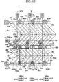
In FIGS. 3-8, the base electrodes are arranged in two rows. The base electrodes have the same width, but they may have different widths as illustrated in FIGS. 3-8.
In the configuration shown in FIGS. 3-7, the height H0 of the base electrodes disposed in an upper row is equal to the height H0 of the base electrodes disposed in a lower row.
In the configuration shown in FIG. 3, three base electrodes in each row (for a total of six base electrodes) form a basic unit referred to as a dot. Each of subpixel electrodes PE1 and PE2 includes one base electrode.
In each configuration shown in FIGS. 4 and 7, five base electrodes in each row (for a total of ten base electrodes) form a dot.
Each of the subpixel electrodes PE11, PE21, PE12 and PE22 shown in FIG. 4 includes two adjacent base electrodes in a row, and each of the subpixel electrodes PE13 and PE23 includes one base electrode. The connection between the adjacent base electrodes in the row is done at upper and lower corners of the base electrodes, and thus a gap between the base electrodes form a cutout 90U or 90L.
Each of the subpixel electrodes PE31, PE41, PE32 and PE42 shown in FIG. 7 includes two adjacent base electrodes in a column, and each of the subpixel electrodes PE33 and PE43 includes one base electrode.
In each configuration shown in FIGS. 5 and 6, four base electrodes in each row (for a total of eight base electrodes) form a dot.
Each of the subpixel electrodes PE15 and PE24 shown in FIG. 5 includes two adjacent base electrodes in a row, and each of the subpixel electrodes PE14, PE25, PE16 and PE26 includes one base electrode.
Each of the subpixel electrodes PE17 and PE28 shown in FIG. 6 includes two adjacent base electrodes in a row, and each of the subpixel electrodes PE18, PE27, PE19 and PE29 includes one base electrode.
It is noted that the subpixel electrodes PE17 and PE27, or PE18 and PE28 forming a pixel electrode shown in FIG. 6 are diagonally disposed to one another unlike those shown in FIGS. 3-5 and 7.
In the configuration shown in FIG. 8, the height H1 of the base electrodes disposed in an upper row is greater than the height H2 of the base electrodes disposed in a lower row. In exemplary embodiments, it is preferable that the height H1 is from about 1.1 times to about twice that of the height H2.
Still referring to FIG. 8, a dot includes five base electrodes in each row, for a total of ten base electrodes. Each of the subpixel electrodes PE51, PE52 and PE53 includes only one base electrode, each of the subpixel electrodes PE61 and PE63 includes a pair of base electrodes 198U1 and 198L1, or 198U3 and 198L3 disposed in different rows, and the subpixel electrode PE62 includes three adjacent base electrodes disposed in the lower row.
The base electrodes 198U1 and 198L1 or 198U3 and 198L3 forming a subpixel electrode PE61 or PE63 are connected to a connection, which connects adjacent corners of the base electrodes 198U3 and 198L3.
The position and the curved direction of the subpixel electrodes shown in FIGS. 3-8 may be changed and the configurations shown in FIGS. 3-8 may be modified by moving the pixel electrodes with an inversion symmetry or by rotating the pixel electrodes.
Referring to FIG. 1 again, the gray voltage generator 800 generates a plurality of gray voltages related to the transmittance of the pixels PX. However, the gray voltage generator 800 may generate only a portion or a given number of gray voltages (referred to as reference gray voltages) instead of generating all of the gray voltages.
The gate driver 400 is connected to the gate lines of the panel assembly 300 and synthesizes the gate-on voltage Von and the gate-off voltage Voff from an external device to generate gate signals Vg for application to the gate lines.
The data driver 500 is connected to the data lines of the panel assembly 300 and applies data voltages Vd, which are selected from the gray voltages supplied from the gray voltage generator 800, to the data lines. However, the data driver 500 may generate gray voltages for all the grays by dividing the reference gray voltages and select the data voltages Vd from the generated gray voltages when the gray voltage generator 800 generates reference gray voltages.
The signal controller 600 controls the gate driver 400 and the data driver 500, etc.
Each of the driving units 400, 500, 600, 700 and 800 may include at least one integrated circuit (IC) chip mounted on the LC panel assembly 300 or on a flexible printed circuit (FPC) film in a tape carrier package (TCP) type, which are attached to the panel assembly 300. Alternatively, at least one of the processing units 400, 500, 600, 700 and 800 may be integrated into the panel assembly 300 along with the signal lines and the switching elements Qa and Qb. Alternatively, all the processing units 400, 500, 600, 700 and 800 may be integrated into a single IC chip, but at least one of the processing units 400, 500, 600, 700 and 800 or at least one circuit element in at least one of the processing units 400, 500, 600, 700 and 800 may be disposed external to the single IC chip.
Now, the operation of the above-described LCD will be described in detail.
The signal controller 600 is supplied with input image signals R, G and B and input control signals controlling the display thereof from an external graphics controller (not shown). The input image signals R, G and B contain luminance information of each pixel PX, and the luminance has a predetermined number of, for example 1024(=210), 256(=28) or 64(=26) grays. The input control signals include a vertical synchronization signal Vsync, a horizontal synchronization signal Hsync, a main clock MCLK and a data enable signal DE, etc.
After generating gate control signals CONT1, data control signals CONT2 and processing the input image signals R, G and B suitable for the operation of the panel assembly 300 and the data driver 500 on the basis of the input control signals and the input image signals R, G and B, the signal controller 600 transmits the gate control signals CONT1 to the gate driver 400, and the processed image signals DAT and the data control signals CONT2 to the data driver 500. The output image signals DAT to the data driver 500 are digital signals having a predetermined number of values (or grays).
The gate control signals CONT1 include a scanning start signal STV for instructing to start scanning and at least a clock signal for controlling the output time of the gate-on voltage Von. The gate control signals CONT1 may further include an output enable signal OE for defining the duration of the gate-on voltage Von.
The data control signals CONT2 include a horizontal synchronization start signal STH for informing of start of data transmission for a group of subpixels, a load signal LOAD for instructing the data voltages to be applied to the panel assembly 300 and a data clock signal HCLK. The data control signal CONT2 may further include an inversion signal RVS for reversing the polarity of the data voltages (with respect to the common voltage Vcom).
Responsive to the data control signals CONT2 from the signal controller 600, the data driver 500 receives a packet of the image data DAT for the group of subpixels from the signal controller 600. The data driver 500 converts the image data DAT into analog data voltages selected from the gray voltages supplied from the gray voltage generator 800, and applies the data voltages to the data lines.
The gate driver 400 applies the gate-on voltage Von to the gate line in response to the gate control signals CONT1 from the signal controller 600, thereby turning on the switching elements connected thereto. The data voltages applied to the data lines are supplied to the subpixels through the activated switching elements.
Referring to FIGS. 3-8, when two subpixel electrodes PE1 and PE2, or PEij and PE(i+1)j, forming a pixel electrode are coupled to respective switching elements, that is, when each of the subpixels includes its own switching element, the two subpixels may be supplied with respective data voltages through the same data line at different times or through different data lines at the same time. However, when one of the subpixel electrodes PE1, PE2, PEij and PE(i+1)j is coupled to a switching element (not shown) and the other of the subpixel electrodes PE1, PE2, PEij and PE(i+1)j is capacitively coupled thereto, the subpixel including the switching element may be directly supplied with data voltages, while the other subpixel may have a voltage that varies depending thereon. At this time, a smaller one of the subpixel electrodes PE1, PE2, PEij and PE(i+1)j preferably has a voltage (relative to the common voltage) greater than a larger one of the subpixel electrodes PE1, PE2, PEij and PE(i+1)j.
In contrast, after two subpixel electrodes PE1, PE2, PEij and PE(i+1)j are charged with the same voltage, the voltages of the subpixel electrodes PE1, PE2, PEij and PE(i+1)j may be differentiated from each other by using storage capacitors (not shown), etc.
Referring to FIGS. 1 and 2, when the voltage difference is generated between two terminals of the LC capacitor Clc1/Clc2, a primary electric field substantially perpendicular to the surfaces of the panels 100 and 200 is generated in the LC layer 3, as both the pixel electrodes PE and the common electrode CE are commonly referred to as field generating electrodes. The LC molecules in the LC capacitor Clc1/Clc2 tend to change their orientations in response to the electric field so that their long axes may be perpendicular to the field direction. The molecular orientations determine the polarization of light passing through the LC layer 3. The polarizer(s) converts the light polarization into the light transmittance such that the pixels PX display the luminance represented by the image data DAT.
The tilt angle of the LC molecules depends on the strength of the electric field. Since the voltages of the LC capacitors Clc1 and Clc2 are different from each other, the tilt angles of the LC molecules in the subpixels are different from each other and thus the luminances of the two subpixels are different. Accordingly, the voltages of the two subpixels can be adjusted so that an image viewed from a lateral side is similar to an image viewed from the front. That is, a lateral gamma curve is similar to or approaches the front gamma curve, thereby improving the lateral visibility.
In addition, the subpixel electrode PE1, PE2, PEij or PE(i+1)j having a voltage (relative to the common voltage Vcom) higher than the other subpixel electrode of a pixel may have an area smaller than the other one, thereby making the lateral gamma curve further approach the front gamma curve. In particular, when the ratio of the areas of the two subpixel electrodes PE1, PE2, PEij and PE(i+1)j is equal to from about 1:2 to about 1:3, the lateral gamma curve further approaches the front gamma curve to further improve the lateral visibility. Since the exemplary embodiments of the present invention can easily adjust the width and the height of the subpixel electrodes PE1, PE2, PEij and PE(i+1)j in each group of the pixel electrodes PE, the area ratio of the two subpixel electrodes PE1, PE2, PEij and PE(i+1)j can be easily adjusted.
The tilt direction of the LC molecules is first determined by a horizontal field component. The horizontal field component is generated by the protrusions 280, the cutouts 90U, 90L, 60U and 60L of the field generating electrodes PE and CE and the edges of the pixel electrodes PE, all of which distort the primary electric field. The horizontal field component is substantially perpendicular to a direction of extension of the protrusions 280, the edges of the cutouts 90U, 90L, 60U and 60L and the edges of the subpixel electrodes PE1, PE2, PEij and PE(i+1)j.
Referring to FIGS. 3-9C, since the LC molecules on each of the sub-areas divided by a set of the protrusions 280 and the cutouts 90U, 90L, 60U and 60L tilt perpendicular to the major edges of the sub-area, the azimuthal distribution of the tilt directions are localized to four directions. Thereby, the reference viewing angle of the LCD is increased.
In the meantime, the direction of a secondary electric field due to the voltage difference between the subpixel electrodes PE1, PE2, PEij and PE(i+1)j is perpendicular to the major edges of the sub-areas. Accordingly, the field direction of the secondary electric field coincides with that of the horizontal component of the primary electric field. Consequently, the secondary electric field between the subpixel electrodes PE1, PE2, PEij and PE(i+1)j enhances the determination of the tilt directions of the LC molecules.
By repeating this procedure by a unit of a horizontal period (which is denoted by “1H” and equal to one period of the horizontal synchronization signal Hsync or the data enable signal DE), all of the pixels PX are supplied with data voltages.
When the next frame starts after one frame finishes, the inversion control signal RVS applied to the data driver 500 is controlled such that the polarity of the data voltages is reversed (which is referred to as “frame inversion”). The inversion control signal RVS may be also controlled such that the polarity of the image data signals flowing in a data line are periodically reversed during one frame (for example, row inversion and dot inversion), or the polarity of the image data signals in one packet are reversed (for example, column inversion and dot inversion).
Now, structures of LC panel assemblies will be described in detail with reference to FIGS. 10A, 10B, 11, 12, 13, 14, 15, 16, 17 and 18 in conjunction with reference to FIGS. 1 and 2.
FIGS. 10A and 10B show schematic equivalent circuit diagrams of the signal lines and pixels PX.
The LC panel assembly shown in FIGS. 10A and 10B includes a plurality of signal lines and a plurality of pixels PX connected thereto. The signal lines include a plurality of gate lines GLa and GLb and a plurality of data lines DL, DL1 and DL2. The signal lines shown in FIG. 10A further include a plurality of storage electrode lines SL extending substantially parallel to the pair of gate lines GLa and GLb.
Each pixel PX includes a pair of subpixels PXa and PXb. Each subpixel PXa/PXb includes a switching element Qa/Qb connected to a respective one of the gate lines GLa and GLb and one of the data lines DL, DL1 and DL2 and a respective LC capacitor Clca/Clcb coupled to the switching element Qa/Qb. Each subpixel PXa/PXb shown in FIG. 10A further includes a corresponding storage capacitor Csta/Cstb connected between the respective switching element Qa/Qb and the storage electrode line SL. It is noted that the two subpixels PXa and PXb shown in FIG. 10A are connected to the same data line DL, while the two subpixels PXa and PXb shown in FIG. 10B are connected to different data lines DL1 and DL2.
Referring to FIGS. 2, 10A and 10B, the switching element Qa/Qb, such as a thin film transistor (TFT), is provided on the lower panel 100 and has three terminals: (1) a control terminal connected to a gate line GLa/GLb; (2) an input terminal connected to a data line DL/DL1/DL2; and (3) an output terminal connected to the LC capacitor Clca/Clcb.
The storage capacitor Csta/Cstb is an auxiliary capacitor for the LC capacitor Clca/Clcb, respectively. The storage capacitor Csta/Cstb includes a subpixel electrode and a separate signal line, which is provided on the lower panel 100, overlapping the subpixel electrode via an insulator, and is supplied with a predetermined voltage such as the common voltage Vcom. Alternatively, the storage capacitor Csta/Cstb includes the subpixel electrode and an adjacent gate line, called a previous gate line, which overlaps the pixel electrode Csta/Cstb via an insulator.
Since the LC capacitor Clca/Clcb and other associated elements are described above with reference to FIG. 2, detailed description thereof will be omitted.
In the LCD shown in FIGS. 10A and 10B with reference to FIG. 1, the signal controller 600 receives input image data R, G and B and converts each input image data R, G and B for each pixel into a plurality of output image data DAT for two subpixels PXa and PXb to be supplied to the data driver. Otherwise, the gray voltage generator 800 generates separate groups of gray voltages for two subpixels PXa and PXb. The two groups of gray voltages are alternatively supplied by the gray voltage generator 800 to the data driver 500 or alternatively selected by the data driver 500. In either case, the two subpixels PXa and PXb are supplied with different voltages.
The values of the converted output image signals and the values of the gray voltages in each group are preferably determined such that the synthesis of gamma curves for the two subpixels PXa and PXb approaches a reference gamma curve at a front view. For example, the synthesized gamma curve at a front view coincides with the most suitable reference gamma curve at a front view, and the synthesized gamma curve at a lateral view is the most similar to the reference gamma curve at a front view.
Now, an example of an LC panel assembly shown in FIG. 10A according to an exemplary embodiment of the present invention will be described in detail with reference to FIGS. 11-14 and FIG. 8.
FIG. 11 is a plan view layout of a lower panel (TFT array panel) according to an exemplary embodiment of the present invention. FIG. 12 is a plan view layout of an upper panel (common electrode panel) according to an exemplary embodiment of the present invention. FIG. 13 is a plan view layout of an LC panel assembly including the TFT array panel shown in FIG. 11 and the common electrode panel shown in FIG. 12. FIG. 14 is a cross-sectional view of the LC panel assembly shown in FIG. 13 taken along lines XIV-XIV.
Referring to FIG. 14, an LC panel assembly according to an exemplary embodiment of the present invention includes a TFT array panel 100, a common electrode panel 200 facing the TFT array panel 100, and a liquid crystal layer 3 interposed between the panels 100 and 200.
First, the TFT array panel 100 will be described with reference to FIGS. 11, 13 and 14.
A plurality of gate conductors including a plurality of pairs of first and second gate lines 121 a and 121 b, respectively, and a plurality of storage electrode lines 131 are formed on an insulating substrate 110, such as transparent glass or plastic, for example.
The gate lines 121 a and 121 b transmit gate signals, extend substantially in a transverse direction and are disposed at relatively upper and lower positions, respectively.
Each of the first gate lines 121 a includes a plurality of first gate electrodes 124 a projecting toward downward and an end portion 129 a having a large area for contact with another layer or an external driving circuit. Each of the second gate lines 121 b includes a plurality of second gate electrodes 124 b projecting upward and toward an end portion 129 b having a large area for contact with another layer or an external driving circuit. The gate lines 121 a and 121 b may extend to be connected to a gate driver 400 that may be integrated on the substrate 110.
The storage electrode lines 131 are supplied with a predetermined voltage such as the common voltage Vcom and extend substantially parallel to the gate lines 121 a and 121 b. Each of the storage electrode lines 131 is disposed between first and second gate lines 121 a and 121 b and is disposed closer to the first gate line 121 a than the second gate line 121 b. Each of the storage electrode lines 131 includes a plurality of storage electrodes 137 (see FIGS. 11 and 13) expanding upward and downward. However, the storage electrode lines 131 may have various shapes and arrangements.
The gate conductors 121 a, 121 b and 131 are preferably made of Al containing metal such as Al and Al alloy, Ag containing metal such as Ag and Ag alloy, Cu containing metal such as Cu and Cu alloy, Mo containing metal such as Mo and Mo alloy, Cr, Ta, or Ti. However, the gate conductors may have a multi-layered structure including two conductive films (not shown) having different physical characteristics. One of the two films is preferably made of low resistivity metal including Al containing metal, Ag containing metal and Cu containing metal for reducing signal delay or voltage drop. The other film is preferably made of a material such as Mo containing metal, Cr, Ta, or Ti, which has good physical, chemical, and electrical contact characteristics with other materials such as indium tin oxide (ITO) or indium zinc oxide (IZO). Suitable examples of the combination of the two films include a lower Cr film and an upper Al (alloy) film and a lower Al (alloy) film and an upper Mo (alloy) film. However, the gate conductors 121 a, 121 b and 131 may be made of various metals or conductors that are currently known or those that will later become known.
The lateral sides of the gate conductors 121 a, 121 b and 131 are inclined relative to a surface of the substrate, and the inclination angle thereof ranges about 30 degrees to about 80 degrees.
A gate insulating layer 140 preferably made of silicon nitride (SiNx) or silicon oxide (SiOx) is formed on the gate conductors 121 a, 121 b and 131.
A plurality of first and second semiconductor islands 154 a and 154 b preferably made of hydrogenated amorphous silicon (abbreviated to “a-Si”) or polysilicon are formed on the gate insulating layer 140. The first/second semiconductor islands 154 a/154 b are disposed on the first/second gate electrodes 124 a/124 b, respectively.
A plurality of pairs of ohmic contact islands 163 b and 165 b are formed on the semiconductor islands 154 b, and a plurality of pairs of ohmic contact islands (not shown) are formed on the semiconductor islands 154 a. The ohmic contact islands 163 b and 165 b are preferably made of n+hydrogenated a-Si heavily doped with n type impurity such as phosphorous or they may be made of silicide.
The lateral sides of the semiconductor islands 154 a and 154 b and the ohmic contacts 163 b and 165 b are inclined relative to the surface of the substrate 110, and the inclination angles thereof are preferably in a range of about 30 degrees to about 80 degrees.
A plurality of data conductors including a plurality of data lines 171 and a plurality of pairs of first and second drain electrodes 175 a and 175 b are formed on the ohmic contacts 163 b and 165 b and the gate insulating layer 140.
The data lines 171 transmit data signals and extend substantially in the longitudinal direction to intersect the gate lines 121 a and 121 b and the storage electrode lines 131. Each data line 171 includes a plurality of first and second source electrodes 173 a and 173 b projecting toward the first and the second gate electrodes 124 a and 124 b, respectively, and the first and the second source electrodes 173 a and 173 b are curved like the letter character “C”. The data lines 171 may extend to be connected to a data driver 500 that may be integrated on the substrate 110.
The first and the second drain electrodes 175 a and 175 b are separated from each other and separated from the data lines 171. The first/second drain electrodes 175 a/175 b are disposed opposite the first/second source electrodes 173 a/173 b with respect to the first/second gate electrodes 124 a/124 b, respectively. Each of the first/second drain electrodes 175 a/175 b includes a wide end portion 177 a/177 b, respectively, and a narrow end portion. The wide end portion 177 a/177 b overlaps a storage electrode 137 and the narrow end portion partly enclosed by a first/second source electrode 173 a/.
A first/second gate electrode 124 a/124 b, a first/second source electrode 173 a/173 b and a first/second drain electrode 175 a/175 b along with a first/second semiconductor island 154 a/154 b form a first/second TFT Qa/Qb having a channel formed in the first/second semiconductor island 154 a/154 b disposed between the first/second source electrode 173 a/173 b and the first/second drain electrode 175 a/175 b, respectively. The first/second TFT Qa/Qb is disposed left/right to a data line 171 disposed therebetween.
The data conductors 171, 175 a and 175 b are preferably made of a refractory metal such as Cr, Mo, Ta, Ti or alloys thereof. However, they may have a multilayered structure including a refractory metal film (not shown) and a low resistivity film (not shown). Suitable examples of the multi-layered structure are a double-layered structure including a lower Cr/Mo (alloy) film and an upper Al (alloy) film and a triple-layered structure of a lower Mo (alloy) film, an intermediate Al (alloy) film and an upper Mo (alloy) film. However, the data conductors 171, 175 a and 175 b may be made of various metals or conductors that are currently known or those that will later become known.
The data conductors 171, 175 a and 175 b have inclined edge profiles, and the inclination angles thereof range about 30 degrees to about 80 degrees.
The ohmic contacts 163 b and 165 b are interposed only between the underlying semiconductor islands 154 a and 154 b and the overlying data conductors 171, 175 a and 175 b thereon and reduce the contact resistance therebetween. The semiconductor islands 154 a and 154 b include some exposed portions, which are not covered with the data conductors 171, 175 a and 175 b, such as portions located between the source electrodes 173 and the drain electrodes 175 a and 175 b.
A passivation layer 180 is formed on the data conductors 171, 175 a and 175 b and the exposed portions of the semiconductor islands 154 a and 154 b. The passivation layer 180 is preferably made of an inorganic or organic insulator and it may have a flat top surface. Examples of the inorganic insulator include silicon nitride and silicon oxide, but is not limited thereto. The organic insulator may have photosensitivity and a dielectric constant less than about 4.0. The passivation layer 180 may include a lower film of an inorganic insulator and an upper film of an organic insulator such that the passivation layer 180 takes the excellent insulating characteristics of the organic insulator while preventing the exposed portions of the semiconductor islands 154 a and 154 b from being damaged by the organic insulator.
The passivation layer 180 has a plurality of contact holes 182, 185 a and 185 b exposing the end portions 179 of the data lines 171 and the first and the second drain electrodes 175 a and 175 b, respectively. The passivation layer 180 and the gate insulating layer 140 have a plurality of contact holes 181 a and 181 b exposing the end portions 129 a and 129 b of the gate lines 121 a and 121 b.
A plurality of pixel electrodes 191R, 191G and 191B and a plurality of contact assistants 81 a, 81 b and 82 are formed on the passivation layer 180. They are preferably made of transparent conductor such as ITO or IZO or a reflective conductor such as Ag, Al, Cr or alloys thereof.
The pixel electrodes 191R, 191G and 191B have the structure shown in FIG. 8 and each pixel electrode 191R/191G/191B includes a pair of subpixels 191Ra and 191Rb/191Ga and 191Gb/191Ba and 191Bb. The subpixel electrodes 191Ra, 191Rb, 191Ga, 191Ba and 191Bb include cutouts 91 a and 91 b, and the subpixel electrode 191 b has a pair of cutouts 92.
The second subpixel electrode 191Rb/191Bb includes first and second unit electrodes 191Rb1 and 191Rb2/191Bb1 and 191Bb2 connected by a connection 192R/192B. It is preferable that the first unit electrode 191Rb1/191Bb1 has a height greater than a height of the second unit electrode 191Rb2/191Bb2, and more preferably, the height of the first unit electrode 191Rb1/191Bb1 is from about 1.1 times to about twice the height of the second unit electrode 191Rb2/191Bb2. When the first subpixel electrode 191Ra/191Ba has a height equal to the height of the first unit electrode 191Rb1/191Bb1, the ratio of areas of the first subpixel electrode 191Ra/191Ba and the second subpixel electrode 191Rb/191Bb is equal to from about 1:1.5 to about 1:2. A desired area ratio can be obtained by adjusting the width and the height of the first subpixel electrode 191Ra/191Ba and the first and the second unit electrodes 191Rb1, 191Rb2, 191Bb1 and 191Bb2 of the second subpixel electrode, and the area ratio is preferably equal to from about 1:1.1 to about 1:3.
The second subpixel electrode 191RG includes three unit electrodes. A pair of cutouts 92 trisects the second subpixel electrode 191Gb. Each of the cutouts 92 includes a curved portion substantially parallel to a curved edge of the second subpixel electrode 191Gb and a transverse portion connected to the curved portion. The width of the second subpixel electrode 191Gb is greater than the width of the first subpixel electrode 191Ga, for example, about three times the width of the first subpixel electrode 191Ga. The height of the second subpixel electrode 191Gb is preferably from about ½ the height to about the same height of the first subpixel electrode 191Ga. The area ratio can be controlled by adjusting the width and the height of the first and the second subpixel electrode 191Ga, 191Gb, and the area ratio is preferably equal to from about 1:1.1 to about 1:3.
The area of the pixel electrodes 191R, 191G and 191B can be uniform by adjusting the width and the height of the subpixel electrodes 191Ra, 191Rb, 191Ga, 191Gb, 191Ba and 191Bb.
Three pixel electrodes 191R, 191G and 191B representing three primary colors such as red, green and blue form a group of pixel electrodes or a dot. The configuration of the subpixel electrodes 191Ra, 191Rb, 191Ga, 191Gb, 191Ba and 191Bb in this exemplary embodiment make the shapes of the pixel electrodes 191R, 191G or 191B, which represent the same color and belong to adjacent dots, substantially the same. In addition, the shapes of the dots are substantially the same. Therefore, the configuration according to this exemplary embodiment improves the display quality of longitudinal lines.
Furthermore, since the width and the height of the subpixel electrodes 191Ra, 191Rb, 191Ga, 191Gb, 191Ba and 191Bb are easily changed in a dot, the areas of the pixel electrodes 191R, 191G and 191B are easily changed.
This exemplary embodiment improves the aperture ratio and the transmittance of a large display device, such as a display device having a size larger than 32 inches or more.
The first subpixel electrodes 191Ra, 191Ga and 191Ba are physically and electrically connected to the first drain electrodes 175 a through the contact holes 185 a such that the subpixel electrode 191Ra, 191Ga and 191Ba receives data voltages from the first drain electrodes 175 a. The second subpixel electrodes 191 b are physically and electrically connected to the second drain electrodes 175 b through the contact holes 185 b such that the subpixel electrodes 191 b receive data voltages from the second drain electrodes 175 b.
A subpixel electrode 191Ra, 191Rb, 191Ga, 191Gb, 191Ba or 191Bb and the common electrode 270 (FIG. 14) form a LC capacitor Clca or Clcb, which stores applied voltages after the TFT turns off.
Storage capacitors Csta/Cstb for enhancing the charge storing capacity are formed by overlapping the first/second subpixel electrodes 191Ra, 191Ga and 191Ba/191Ra, 191Ga and 191Ba and the drain electrodes 175 a/175 b with the storage electrodes 137, etc.
The storage electrode lines 131, the wide end portions 177 a and 177 b of the first and the second drain electrodes 175 a and 175 b, the contact holes 185 a and 185 b, and the second gate lines 121 b are disposed near boundaries of adjacent rows of the unit electrodes. This configuration covers texture that appears near the boundaries of adjacent rows of the unit electrodes due to the disorder of the molecular orientations, and increases the aperture ratio.
The contact assistants 81 a, 81 b and 82 are connected to the end portions 129 a and 129 b of the gate lines 121 a and 121 b, respectively, and the end portions 179 of the data lines 171 through the contact holes 181 a, 181 b and 182, respectively. The contact assistants 81 a, 81 b and 82 protect the end portions 129 a, 129 b and 179 and enhance the adhesion between the end portions 129, 129 b and 179 and external devices.
The description of the common electrode panel 200 follows with reference to FIGS. 12-14.
A light blocking member 220 referred to as a black matrix for preventing light leakage is formed on an insulating substrate 210 such as transparent glass or plastic. The light blocking member 220 includes a plurality of curved portions (see FIG. 12) facing the data lines 171 (see FIG. 13) on the TFT array panel 100 and a plurality of widened portions facing the TFTs Qa and Qb on the TFT array panel 100. However, the light blocking member 220 may have various shapes for blocking light leakage near the pixel electrodes 191R, 191G and 191B and the TFTs Qa and Qb.
A plurality of color filters 230R and 230G are also formed on the substrate 210 and the light blocking member 220 and they are disposed substantially in the areas enclosed by the light blocking member 220. The color filters 230R and 230G may extend substantially in the longitudinal direction along the pixel electrodes 191R, 191G and 191B. The color filters 230R represent red color, the color filters 230G represent green color and other color filters (not shown) may represent blue color.
An overcoat 250 is formed on the color filters 230R and 230G and the light blocking member 220. The overcoat 250 is preferably made of an (organic) insulator and it prevents the color filters 230R and 230G from being exposed and provides a flat surface. However, it will be recognized that the overcoat 250 may be omitted.
A common electrode 270 is formed on the overcoat 250 (FIG. 14). The common electrode 270 is preferably made of a transparent conductive material such as ITO and IZO and has a plurality of sets of cutouts 71Ra, 71Rb1. 71Rb2, 71Ga, 71Gb, 71Ba, 71Bb1 and 71Bb2, which are described above with reference to FIG. 8.
The number of the cutouts 71Ra, 71Rb1. 71Rb2, 71Ga, 71Gb, 71Ba, 71Bb1 and 71Bb2 may be varied depending on the design factors, and the light blocking member 220 may also overlap the cutouts 71Ra, 71Rb1. 71Rb2, 71Ga, 71Gb, 71Ba, 71Bb1 and 71Bb2 to block the light leakage through the cutouts 71Ra, 71Rb1. 71Rb2, 71Ga, 71Gb, 71Ba, 71Bb1 and 71Bb2.
Alignment layers 11 and 21 that may be homeotropic are coated on inner surfaces of the panels 100 and 200.
Polarizers 12 and 22 are provided on outer surfaces of the panels 100 and 200 so that their polarization axes may be crossed or transverse to one another and the polarization axes may make about 45 degrees with the curved edges of the subpixel electrodes 191Ra, 191Rb, 191Ga, 191Gb, 191Ba and 191Bb for increasing light efficiency. It will be recognized that one of the polarizers 12 and 22 may be omitted when the LCD is a reflective LCD.
The LCD may further include at least one retardation film (not shown) for compensating the retardation of the LC layer 3. The LCD may further include a backlight unit (not shown) supplying light to the LC layer 3 through the polarizers 12 and 22, the retardation film and the panels 100 and 200.
It is preferable that the LC layer 3 has negative dielectric anisotropy and is subjected to a vertical alignment.
The shapes and the arrangements of the cutouts 71Ra, 71Rb1. 71Rb2, 71Ga, 71Gb, 71Ba, 71Bb1, 71Bb2, 91 a, 91 b and 92 may be modified, as recognized by those skilled in the pertinent art.
At least one of the cutouts 71Ra, 71Rb1. 71Rb2, 71Ga, 71Gb, 71Ba, 71Bb1, 71Bb2, 91 a, 91 b and 92 may be substituted with protrusions (not shown) or depressions (not shown). The protrusions are preferably made of an organic or inorganic material and disposed on or under the field generating electrodes 191R, 191G, 191B or 270.
Another example of a LC panel assembly shown in FIG. 10A according to another exemplary embodiment of the present invention will be described in detail with reference to FIGS. 15-18.
FIG. 15 is a plan view layout of a TFT array panel according to another exemplary embodiment of the present invention. FIG. 16 is a plan view layout of a common electrode panel according to another exemplary embodiment of the present invention. FIG. 17 is a plan view layout of an LC panel assembly including the TFT array panel shown in FIG. 15 and the common electrode panel shown in FIG. 16. FIG. 18 is a cross-sectional view of the LC panel assembly shown in FIG. 17 taken along lines XVIII-XVIII.
The LC panel assembly according to the exemplary embodiment illustrated in FIGS. 15-18 includes a TFT array panel 100, a common electrode panel 200 facing the TFT array panel 100, a liquid crystal layer 3 and a pair of polarizers 12 and 22.
Layered structures of the LC panel assembly according to this exemplary embodiment are almost the same as those shown in FIGS. 11-14.
Regarding the TFT array panel 100, gate conductors including a plurality of first and second gate lines 121 a and 121 b and a plurality of first and second storage electrode lines 131 a and 131 b are formed on a substrate 110. The first and the second gate lines 121 a and 121 b include first and second gate electrodes 124 a and 124 b and end portions 129 a and 129 b, respectively. The first and the second storage electrode lines 131 a and 131 b include first and second storage electrodes 137 a and 137 b. The second storage electrode lines 131 b further include third storage electrodes 136 b. A gate insulating layer 140, a plurality of semiconductor members 154 a and 154 b and a plurality of ohmic contacts 163 a and 165 a are sequentially formed on the gate conductors 121 a, 121 b, 131 a and 131 b. Data conductors including a plurality of data lines 171 and a plurality of first and second drain electrodes 175 a and 175 b are formed on the ohmic contacts 163 a and 165 a. The data lines 171 include first and second source electrodes 173 a and 173 b and end portions 179. The drain electrodes 175 a and 175 b include wide end portions 177 a and 177 b overlapping the first and the second storage electrodes 137 a and 137 b, respectively. A passivation layer 180 is formed on the data conductors 171, 175 a and 175 b, the gate insulating layer 140 and exposed portions of the semiconductor members 154 a and 154 b. A plurality of contact holes 181 a, 181 b, 182, 185 a and 185 b are provided at the passivation layer 180 and the gate insulating layer 140. A plurality of pixel electrodes 191R, 191G and 191B including subpixel electrodes 191Ra, 191Rb, 191Ga, 191Gb, 191Ba and 191 Bb having cutouts 91 a, 91 b and 92, and a plurality of contact assistants 81 a, 81 b and 82 are formed on the passivation layer 180. An alignment layer 11 is then coated thereon.
Regarding the common electrode panel 200, a light blocking member 220, an overcoat 250, a common electrode 270 having a plurality of cutouts 71Ra, 71Rb1, 71Rb2, 71Ga, 71Gb, 71Ba, 71Bb1 and 71Bb2 and an alignment layer 21 are formed on an insulating substrate 210.
Different from the LC panel assembly shown in FIGS. 11-14, the first gate lines 121 a are disposed near boundaries of adjacent rows of the unit electrodes.
The first and the second storage electrode lines 131 a and 131 b, the wide end portions 177 a and 177 b of the first and the second drain electrodes 175 a and 175 b and the contact holes 185 a and 185 b are disposed near boundaries of adjacent rows of the unit electrodes. This configuration covers texture that appears near the boundaries due to the disorder of the molecular orientations, and increases the aperture ratio.
Furthermore, storage capacitors Csta and Cstb and the contact holes 185 a and 185 b are disposed under the cutouts 71Ra, 71Rb2, 71Ga, 71Gb, 71Ba and 71Bb2 to cover texture near the cutouts 71Ra, 71Rb2, 71Ga, 71Gb, 71Ba and 71Bb2.
The first drain electrodes 175 a further include projections 176 a extending from the wide end portions 177 a along the first storage electrode lines 131 a. The second drain electrodes 175 b further include expansions 176 b connected to the wide end portions 177 b and overlapping the third storage electrodes 136 b.
The configuration facilitates the control of the overlapping area between the storage electrodes 137 a, 137 b and 136 b and the drain electrodes 175 a and 175 b and the capacitance of the storage capacitors Csta and Cstb.
Both first and second TFTs Qa and Qb are disposed right onto the data lines 171 to reduce the defect due to the alignment errors. The distance between the data lines 171 and the overlapping area between the data lines and the pixel electrodes 191R, 191G and 191B are easily adjusted. The parasitic capacitance between the data lines 171 and the pixel electrodes 191R, 191G and 191B can also be adjusted.
Each of oblique portions of the cutouts 71Ra, 71Rb1, 71Rb2, 71Ga, 71Gb, 71Ba, 71Bb1 and 71Bb2 of the common electrode 270 has at least one depressed notch.
In addition, the TFT array panel 100 shown in FIGS. 15-18 includes a plurality of color filters 230R disposed under the passivation layer 180, while the common electrode panel 200 has no color filter and no overcoat. The color filters 230R extend along a longitudinal direction and are periodically curved and are not provided in peripheral areas where the end portions 129 and 179 of the gate lines 121 and the data lines 171 are disposed. The color filters 230R have through holes 235 larger than the contact holes 185 a so that the contact holes 185 a may pass through the through holes 235.
Adjacent color filters 230R overlap each other on the data lines 171 to block the light leakage between the pixel electrodes 191R, 191G and 191B similar to the light blocking member 220. In this case, the light blocking member 220 disposed on a common electrode panel 200 may be omitted to simplify the manufacturing process.
Another passivation layer (not shown) may be formed under the color filters 230R.
This exemplary embodiment increases the transmitting area for incident light to improve the aperture ratio and the light transmittance.
Many of the above-described features of the LC panel assembly shown in FIGS. 11-14 may be applicable to the LC panel assembly shown in FIGS. 15-18.
Other examples of a LC panel assembly shown in FIGS. 10A and 10B according to other exemplary embodiments of the present invention will now be described in detail with reference to FIGS. 19-24.
FIGS. 19, 21, 22, 23 and 24 are plan view layouts of a LC panel assembly according to other exemplary embodiments of the present invention. FIG. 20 is a cross-sectional view of the LC panel assembly shown in FIG. 19 taken along lines XX-XX.
The LC panel assemblies shown in FIGS. 19, 21, 22, 23 and 24 have pixel electrode configurations shown in FIGS. 3, 4, 5, 6 and 7, respectively.
An LC panel assembly includes a TFT array panel 100, a common electrode panel 200 facing the TFT array panel 100 and a liquid crystal layer 3.
Layered structures of the LC panel assembly according to these exemplary embodiments are almost the same as those shown in FIGS. 11-14.
Regarding the TFT array panel 100, a plurality of first and second gate lines 121 a and 121 b, respectively, are formed on a substrate 110. The first and the second gate lines 121 a and 121 b include first and second gate electrodes 124 a and 124 b, respectively. A gate insulating layer 140 is formed on the gate lines 121 a and 121 b and a plurality of semiconductor members 154 a and 154 b are formed on the gate insulating layer 140. A plurality of pairs of ohmic contact contacts 163 a and 165 a are formed on the semiconductor members 154 a. A plurality of pairs of ohmic contact contacts (not shown) are formed on the semiconductor members 154 b. Data conductors including a plurality of data lines 171 and a plurality of drain electrodes 175 a and 175 b are formed on the ohmic contacts 163 a and 165 a. The data lines 171 include source electrodes 173 a and 173 b. A passivation layer 180 is formed on the data conductors 171, 175 a and 175 b, the gate insulating layer 140 and exposed portions of the semiconductor members 154 a and 154 b. A plurality of contact holes 185 a and 185 b are provided at the passivation layer 180. A plurality of pixel electrodes 191, 191R, 191G and 191B including subpixel electrodes 191 a, 191 b, 191Ra, 191Rb, 191Ga, 191Gb, 191Ba and 191 Bb having cutouts 93 a and 93 b are formed on the passivation layer 180.
Regarding the common electrode panel 200, a light blocking member 220, a plurality of color filters 230 and a common electrode 270 are formed on an insulating substrate 210.
Different from the LC panel assembly shown in FIGS. 11-14, a plurality of protrusions 280 are formed on the common electrode 270, however, the common electrode 270 has no cutout. The protrusions 280 are made of dielectrics and have a saw tooth shape. The protrusions 280 bisect the color filters 230.
The subpixel electrodes 191 a, 191 b, 191Ra, 191Rb, 191Ga, 191Gb, 191Ba and 191Bb of some or all of the pixels are coupled to different data lines 171, and thus the source electrodes 173 a and 173 b of a data line 171 are disposed at left and right sides of the data line 171.
In this configuration, an apparent inversion type, which appears over the pixels in the panel assembly, can be made to be dot inversion. In contrast, a driver inversion type, which is driven by the data driver 500 through the data lines 171, is made to be column inversion. Accordingly, the advantages of the column inversion and the dot inversion can be exploited. That is, the driver column inversion reduces the signal delay of the data lines 171 and the power consumption, while the apparent dot inversion prevents the flickering from being dominantly recognized.
In the panel assemblies shown in FIGS. 21-24, the area of the pixel electrodes 191R and 191G of the red and green pixels, respectively, is larger than the area of the pixel electrode 191B of the blue pixel. In this manner, when adjusting the width of sub-areas partitioned by the cutouts 93 a and 93 b and the protrusions 280 for improving the response time of the liquid crystal, it is preferable that the area of the blue pixel is reduced since human eyes are relatively insensitive to blue color as compared with red and green colors. In exemplary embodiments, the width of the sub-areas is preferably equal to from about 14 microns to about 25 microns.
When the pixel electrodes 191R, 191G and 191B have different areas, the distance between the data lines 171 may or may not be uniform depending on the arrangements of the subpixel electrode 191Ra, 191Rb, 191Ga, 191Gb, 191Ba and 191Bb. In the case of FIG. 22, upper and lower subpixel electrodes 191Ra, 191Rb, 191Ga and 191Gb of a pixel, which have different sizes, are arranged in a diagonal direction to maintain a uniform distance between the data lines 171.
Many of the above-described features of the LC panel assembly shown in FIGS. 11-14 may be applicable to the LC panel assembly shown in FIGS. 19-24.
Now, a structure of an LC panel assembly according to another exemplary embodiment of the present invention will now be described in detail with reference to FIGS. 25, 26 and 27 in conjunction with FIGS. 1 and 2.
FIG. 25 shows an equivalent circuit diagram of the signal lines and a pixel PX.
The LC panel assembly shown in FIG. 25 includes a plurality of signal lines and a plurality of pixels PX connected thereto. The signal lines include a plurality of gate lines GL, a plurality of pairs of data lines DLc and DLd and a plurality of storage electrode lines SL.
Each pixel PX includes a pair of subpixels PXc and PXd. Each subpixel PXc/PXd includes a switching element Qc/Qd, respectively, connected to one of the gate lines GL and one of the data lines DLc and DLd, a LC capacitor Clcc/Clcd coupled to the switching element Qc/Qd, and a storage capacitor Cstc/Cstd connected between the switching element Qc/Qd and the storage electrode line SL.
The switching element Qc/Qd, such as a thin film transistor (TFT), is provided on the lower panel 100 and has three terminals: (1) a control terminal connected to a gate line GL; (2) an input terminal connected to a data line DLc/DLd; and (3) an output terminal connected to the LC capacitor Clcc/Clcd.
Since the LC capacitor Clcc/Clcd, the storage capacitors Cstc and Cstd and the operation of the LCD including the panel assembly shown in FIG. 25, etc. are substantially the same as those described above, detailed description thereof will be omitted.
However, it is noted that the two pixels PXc and PXd forming a pixel PX shown in FIG. 25 are supplied with data voltages at the same time unlike those shown in FIGS. 10A and 10B.
An example of a LC panel assembly shown in FIG. 25 according to an exemplary embodiment of the present invention will now be described in detail with reference to FIGS. 26 and 27.
FIG. 26 is a layout view of an LC panel assembly according to an exemplary embodiment of the present invention. FIG. 27 is a cross-sectional view of the LC panel assembly shown in FIG. 26 taken along lines XXVII-XXVII.
The LC panel assembly includes a TFT array panel 100, a common electrode panel 200 facing the TFT array panel 100, a liquid crystal layer 3 and a pair of polarizers 12 and 22, referring to FIGS. 26 and 27.
Layered structures of the LC panel assembly according to this exemplary embodiment are similar to those shown in FIGS. 11-14.
Regarding the TFT array panel 100, gate conductors including a plurality of gate lines 121 and a plurality of storage electrode lines 131 are formed on a substrate 110. Each of the gate lines 121 includes first and second gate electrodes 124 c and 124 d and end portions 129. The storage electrode lines 131 include storage electrodes 137. A gate insulating layer 140 is formed on the gate conductors 121 and 131, and a plurality of semiconductor stripes including first and second projections 154 c and 154 d are formed on the gate insulating layer 140. A plurality of ohmic contact stripes 161 including projections 163 c and a plurality of ohmic contacts 165 c are formed on the semiconductor stripes 151. Data conductors including a plurality of pairs of first and second data lines 171 c and 171 d, respectively, and a plurality of first and second drain electrodes 175 c and 175 d, respectively, are formed on the ohmic contacts 161 and 165 a. The first and second data lines 171 c and 171 d include first and second source electrodes 173 c and 173 d and end portions 179 c and 179 d, respectively, and the drain electrodes 175 c and 175 d include wide end portions 177 c and 177 d. A passivation layer 180 is formed on the data conductors 171 c, 171 d, 175 c and 175 d, the gate insulating layer 140 and exposed portions of the semiconductor stripes 151. A plurality of contact holes 181, 182 a, 182 b, 185 a and 185 b are provided at the passivation layer 180 and the gate insulating layer 140. A plurality of pixel electrodes 191R, 191G and 191B including subpixel electrodes 191Rc, 191Rd, 191Gc, 191Gd, 191Bc and 191Bd and a plurality of contact assistants 81, 82 c and 82 d are formed on the passivation layer 180. The second subpixel electrodes 191Rd include first and second unit electrodes 191Rd1 and 191Rd2, and the second subpixel electrodes 191Bd include first and second unit electrodes 191Bd1 and 191Bd2. The subpixel electrodes 191Rc, 191Rd, 191Gc, 191Bc and 191Bd have cutouts 91 c and 91 d, and the subpixel electrode 191Gd has a cutout 92. An alignment layer 11 is coated on the pixel electrodes 191R, 191G and 191B and the passivation layer 180.
Regarding the common electrode panel 200, a light blocking member 220, a plurality of color filters 230R, an overcoat 250, a common electrode 270 having a plurality of cutouts 71Rc, 71Rd1. 71Rd2, 71Gc, 71Gd, 71Bc, 71Bd1 and 71Bd2, and an alignment layer 21 are formed on an insulating substrate 210.
However, the number of the gate lines 121 in the LC panel assembly shown in FIGS. 26 and 27 is a half that in the LC panel assembly shown in FIGS. 11-14, and the number of the data lines 171 c and 171 d in the LC panel assembly shown in FIGS. 26 and 27 is twice that in the LC panel assembly shown in FIGS. 11-14. Furthermore, first and second TFTs Qc and Qd coupled to the first and second subpixel electrodes 191Rc, 191Rd, 191Gc, 191Gd, 191Bc and 191Bd forming a pixel electrode 191R, 191G or 191B are connected to the same gate line 121 and different data lines 171 c and 171 d.
The first and the second TFTs Qc and Qd are disposed to the left of the first and the second data lines 171 c and 171 d, respectively, as illustrated in FIG. 26.
The semiconductors 154 c and 154 d extend along the data lines 171 c and 171 d and the drain electrodes 175 c and 175 d, respectively, to form the semiconductor stripes 151. The semiconductor stripes 151 have almost the same planar shapes as the data conductors 171 c, 171 d, 175 c and 175 d, as well as the underlying ohmic contacts 161 and 165 (see FIG. 27).
A manufacturing method of the TFT array panel according to an exemplary embodiment simultaneously forms the data conductors 171 c, 171 d, 175 c and 175 d, the semiconductors 151 and the ohmic contacts 161 and 165 c using a single photolithography process.
A photoresist pattern for the photolithography process has a position-dependent thickness, and in particular, the photoresist pattern has first and second portions with decreased thickness. The first portions are located on wire areas that will be occupied by the data conductors 171 c, 171 d, 175 c and 175 d and the second portions are located on channel areas of TFTs.
The position-dependent thickness of the photoresist is obtained by several techniques, for example, by providing translucent areas on the exposure mask as well as transparent areas and light blocking opaque areas. The translucent areas may have a slit pattern, a lattice pattern, a thin film(s) with intermediate transmittance or intermediate thickness. When using a slit pattern, it is preferable that the width of the slits or the distance between the slits is smaller than the resolution of a light exposer used for the photolithography. Another example is to use reflowable photoresist. Once a photoresist pattern made of a reflowable material is formed by using a normal exposure mask only with transparent areas and opaque areas, it is subject to reflow process to flow onto areas without the photoresist, thereby forming thin portions.
As a result, the manufacturing process is simplified by omitting a photolithography step.
Many of the above-described features of the LC panel assembly shown in FIGS. 11-14 may be applicable to the LC panel assembly shown in FIGS. 26 and 27.
Now, structures of LC panel assemblies according to other exemplary embodiments of the present invention will be described in detail with reference to FIGS. 28, 29, 30, 31, 32 and 33 in conjunction with FIGS. 1 and 2.
FIG. 28 shows an equivalent circuit diagram of the signal lines and a pixel PX.
The LC panel assembly shown in FIG. 28 includes a plurality of signal lines and a plurality of pixels PX connected thereto. The signal lines include a plurality of gate lines GL and a plurality of data lines DL.
Each pixel PX includes a pair of first and second subpixels PXe and PXf and a coupling capacitor Ccp connected between the first subpixel PXe and the second subpixel PXf.
The first subpixel PXe includes a switching element Q connected to one of the gate lines GL and one of the data lines DL, a first LC capacitor Clce coupled to the switching element Q, and a storage capacitor Cste connected to the switching element Q. The second subpixel PXf includes a second LC capacitor Clcb coupled to the coupling capacitor Ccp.
The switching element Q, such as a thin film transistor (TFT), is provided on the lower panel 100 and has three terminals: (1) a control terminal connected to a gate line GL; (2) an input terminal connected to a data line DL; and (3) an output terminal connected to the LC capacitor Clce, the storage capacitor Cste and the coupling capacitor Ccp.
The switching element Q transmits data voltages from the data line DL in response to gate signals from the gate line GL to the first LC capacitor Clce and the coupling capacitor Ccp. The coupling capacitor Ccp coverts the magnitude of the data voltage and supplied to the second LC capacitor Clcf.
It is assumed that the common voltage Vcom is applied to the storage capacitor Cste and the capacitor Clce, Cste, Clcf or Ccp and the capacitance thereof are denoted by the same numerals, a voltage Ve stored in the first LC capacitor Clce and a voltage Vf stored in the second LC capacitor Clcf satisfies:
Vf=Ve×[Ccp/(Ccp+Clcf)].
Since Ccp/(Ccp+Clcf) is less than one, the voltage Vf stored in the second LC capacitor Clcf is smaller than the voltage Ve stored in the first LC capacitor Clce. The relation is also satisfied even though the voltage applied to the storage capacitor Cste is not the common voltage Vcom.
The desired ratio of the voltages Ve and Vf can be obtained by adjusting the capacitance of the coupling capacitor Ccp.
Examples of a LC panel assembly shown in FIG. 28 according to exemplary embodiments of the present invention will be described in detail with reference to FIGS. 29-33.
FIGS. 29, 31, 32 and 33 are plan view layouts of a LC panel assembly according to exemplary embodiments of the present invention. FIG. 30 is a cross-sectional view of the LC panel assembly shown in FIG. 29 taken along lines XXX-XXX.
The LC panel assemblies shown in FIGS. 29, 31, 32 and 33 have pixel electrode configurations shown in FIGS. 3, 4, 5 and 6, respectively.
An LC panel assembly includes a TFT array panel 100, a common electrode panel 200 facing the TFT array panel 100 and a liquid crystal layer 3.
Layered structures of the LC panel assembly according to these exemplary embodiments are similar to those shown in FIGS. 19-23.
Regarding the TFT array panel 100, a plurality of gate lines 121 are formed on a substrate 110. The gate lines 121 include gate electrodes 124. A gate insulating layer 140, and a plurality of semiconductor members 154 and a plurality of pairs of ohmic contact contacts 163 and 165 are sequentially formed on the gate lines 121. Data conductors including a plurality of data lines 171 and a plurality of drain electrodes 175 are formed on the ohmic contacts 163 and 165 and the gate insulating layer 140. The data lines 171 include source electrodes 173. A passivation layer 180 is formed on the data conductors 171 and 175, the gate insulating layer 140 and exposed portions of the semiconductor members 154. A plurality of contact holes 185 are provided at the passivation layer 180. A plurality of pixel electrodes 191, 191R, 191G and 191B including subpixel electrodes 191 e, 191 f, 191Re, 191Rf, 191Ge, 191Gf, 191Be and 191 Bf having cutouts 93 a and 93 b are formed on the passivation layer 180.
Regarding the common electrode panel 200, a light blocking member 220, a plurality of color filters 230, a common electrode 270 and a plurality of protrusions 280 are formed on an insulating substrate 210.
Different from the LC panel assembly shown in FIGS. 19-23, the second subpixel electrodes 191 f, 191Rf, 191Gf and 191Bf are electrically floating, while the first subpixel electrodes 191 e, 191Re, 191Ge and 191Be are connected to the drain electrodes 175.
Each of the drain electrodes 175 includes a coupling electrode 176 extending to oblique edges of the pixel electrodes 191, 191R, 191G and 191B. The coupling electrode 176 extends along a protrusion 280 under a second subpixel electrode 191 f, 191Rf, 191Gf and 191Bf to overlap the second subpixel electrode 191 f, 191Rf, 191Gf and 191Bf. Therefore, the first subpixel electrode 191 e, 191Re, 191Ge or 191Be and the second subpixel electrode 191 f, 191Rf, 191Gf and 191Bf are capacitively coupled to each other to form a coupling capacitor Ccp.
Many of the above-described features of the LC panel assembly shown in FIGS. 19-23 may be applicable to the LC panel assembly shown in FIGS. 29-33.
Now, structures of the LC panel assemblies will now be described in detail with reference to FIGS. 34, 35, 36, 37 and 38 in conjunction with FIGS. 1 and 2.
FIG. 34 shows a schematic equivalent circuit diagram of the signal lines and a pixel PX.
The LC panel assembly shown in FIG. 34 includes a plurality of signal lines and a plurality of pixels PX connected thereto. The signal lines include a plurality of gate lines GL, a plurality of data lines DL and a plurality of pairs of storage electrode lines SLg and SLh extending substantially parallel to the gate lines GL.
Each pixel PX includes a pair of subpixels PXg and PXh. Each subpixel PXg/PXh includes a switching element Qg/Qh, respectively, connected to one of the gate lines GL and one of the data lines DL, a LC capacitor Clcg/Clch coupled to the switching element Qg/Qh, a storage capacitor Cstg/Csth connected between the switching element Qg/Qh and one of the storage electrode lines SLg/SLh.
The switching element Qg/Qh, such as a TFT, is provided on the lower panel 100 and has three terminals: (1) a control terminal connected to a gate line GL; (2) an input terminal connected to a data line DL; and (3) an output terminal connected to the LC capacitor Clcg/Clch and the storage capacitor Cstg/Csth.
The storage capacitor Cstg/Csth is an auxiliary capacitor for the LC capacitor Clcg/Clch. The storage capacitor Cstg/Csth includes a subpixel electrode and the storage electrode line SLg/SLh, which is provided on the lower panel 100 and overlapping the subpixel electrode via an insulator. The two storage electrode lines SLg and SLh are supplied with periodical voltages having opposite phases or polarities.
Since the LC capacitor Clcg/Clch and other associated elements have been described above with reference to FIG. 2, detailed description thereof will be omitted.
In the LCD shown in FIG. 34, after the LC capacitors Clca and Clcb and the storage capacitors Cstg and Csth are charged and the switching elements Qg and Qh are turned off, the voltages applied to the storage electrode lines SLg and SLh move in opposite directions to differentiate the voltages of the LC capacitors Clcg and Clch.
Examples of a LC panel assembly shown in FIG. 34 according to exemplary embodiments of the present invention will be described in detail with reference to FIGS. 35-38.
FIGS. 35, 36, 37 and 38 are plan view layouts of a LC panel assembly according to exemplary embodiments of the present invention.
The LC panel assemblies shown in FIGS. 35, 36, 37 and 38 have pixel electrode configurations shown in FIGS. 3, 4, 5 and 6, respectively.
An LC panel assembly includes a TFT array panel 100, a common electrode panel 200 facing the TFT array panel 100 and a liquid crystal layer 3.
Layered structures of the LC panel assembly according to these exemplary embodiments are similar to those shown in FIGS. 19-23, and therefore, cross-sectional views thereof are omitted.
Regarding the TFT array panel 100, a plurality of gate lines 121 are formed on a substrate 110. Each of the gate lines 121 includes first and second gate electrodes 124 g and 124 h, respectively. A gate insulating layer 140, a plurality of semiconductor members 154 and a plurality of pairs of ohmic contact contacts (not shown) are sequentially formed on the gate lines 121. Data conductors including a plurality of data lines 171 and a plurality of drain electrodes 175 g and 175 h are formed on the ohmic contacts and the gate insulating layer 140. The data lines 171 include source electrodes 173 g and 173 h. A passivation layer 180 is formed on the data conductors 171, 175 g and 175 h, the gate insulating layer 140 and exposed portions of the semiconductor members 154. A plurality of contact holes 185 g and 185 h are provided at the passivation layer 180. A plurality of pixel electrodes 191, 191R, 191G and 191B including subpixel electrodes 191 g, 191 h, 191Rg, 191Rh, 191Gg, 191Gh, 191Bg and 191 Bh having cutouts 93 a and 93 b are formed on the passivation layer 180.
Regarding the common electrode panel 200, a light blocking member 220, a plurality of color filters 230, a common electrode 270 and a plurality of protrusions 280 are formed on an insulating substrate 210.
Different from the LC panel assembly shown in FIGS. 19-23, only one gate line 121 is assigned to one pixel row, and the gate lines 121 pass through boundaries of the subpixel electrodes 191 g, 191 h, 191Rg, 191Rh, 191Gg, 191Gh, 191Bg and 191Bh. A pair of gate electrodes 124 g and 124 h are connected to each other, and a pair of source electrodes 173 g and 173 h disposed on the pair of gate electrodes 124 g and 124 h are connected to the same data line 171.
A plurality of pairs of storage electrode lines 131 g and 131 h are formed on the substrate 110. Each pair of storage electrode lines 131 g and 131 h are disposed opposite each other with respect to a gate line 121 and supplied with periodic voltages having opposite phases.
Two subpixel electrodes 191 g, 191 h, 191Rg, 191Rh, 191Gg, 191Gh, 191Bg and 191Bh forming a pixel electrode 191, 191R, 191G and 191B overlap respective storage electrode lines 131 g and 131 h forming respective storage capacitors Cstg and Csth.
Many of the above-described features of the LC panel assembly shown in FIGS. 19-23 may be applicable to the LC panel assembly shown in FIGS. 35-38.
In this manner, the aperture ratio and the transmittance are increased to improve the lateral visibility. The capacitance of the storage electrodes, the area of the pixel electrodes, the distance between the data lines and the overlapping area between the data lines and the pixel electrodes, etc. are easily controllable.
While the present invention has been described in detail with reference to the exemplary embodiments, those skilled in the art will appreciate that various modifications and substitutions can be made thereto without departing from the spirit and scope of the present invention as set forth in the appended claims.

Claims (36)

1. A liquid crystal display comprising:
a substrate;
a pixel electrode disposed on the substrate, the pixel electrode including a first subpixel electrode and a second subpixel electrode; and
a common electrode facing the pixel electrode, the common electrode having a cutout,
wherein the first subpixel electrode and the second subpixel electrode are independently capacitively coupled to the common electrode,
the first subpixel electrode includes a first electrode including at least two substantially parallelogram shaped electrode pieces that have different inclination directions and are connected to each other in a longitudinal direction, and
the second subpixel electrode includes a second electrode disposed at a longitudinal side of the first electrode, the second electrode including at least two substantially parallelogram shaped electrode pieces that have different inclination directions and are connected to each other in the longitudinal direction, and
each of the electrode pieces has a pair of oblique edges substantially parallel to each other, and
the cutout passes through the first and the second subpixel electrodes and includes an oblique portion extending substantially parallel to the oblique edges of the electrode pieces.
2. The liquid crystal display of claim 1, wherein the first electrode and the second electrode are adjacent to each other.
3. The liquid crystal display of claim 1, wherein the first electrode and the second electrode are aligned in a diagonal direction relative to one another.
4. The liquid crystal display of claim 1, wherein the first and the second electrodes are aligned at an edge defining the first and the second electrodes.
5. The liquid crystal display of claim 1, wherein the first electrode and the second electrode are aligned at a center defining a joint between the two substantially parallelogram shaped electrode pieces.
6. The liquid crystal display of claim 1, wherein the first electrode and the second electrode have different widths.
7. The liquid crystal display of claim 1, wherein the first electrode and the second electrode have different heights.
8. The liquid crystal display of claim 7, wherein the height of the first electrode is greater than the height of the second electrode and equal to or smaller than twice the height of the second electrodes.
9. The liquid crystal display of claim 1, wherein the second subpixel electrode comprises a third electrode including at least two substantially parallelogram shaped electrode pieces that have different inclination directions, and the third electrode is transversely adjacent to the first electrode and connected to the second electrode.
10. The liquid crystal display of claim 1, wherein the first subpixel electrode and the second subpixel electrode have different areas.
11. The liquid crystal display of claim 10, wherein the area of the second subpixel electrode is from about 1.1 times to about three times the area of the first subpixel electrode.
12. The liquid crystal display of claim 1, wherein the first subpixel electrode and the second subpixel electrode have different voltages.
13. The liquid crystal display of claim 12, wherein the voltages of the first subpixel electrode and the second subpixel electrode are originated from a single image information.
14. The liquid crystal display of claim 13, further comprising:
a first thin film transistor coupled to the first subpixel electrode;
a second thin film transistor coupled to the second subpixel electrode;
first and second signal lines coupled to the first thin film transistor; and
third and fourth signal lines coupled to the second thin film transistor.
15. The liquid crystal display of claim 13, further comprising:
a first thin film transistor coupled to the first subpixel electrode;
a second thin film transistor coupled to the second subpixel electrode;
a first signal line coupled to the first thin film transistor;
a second signal line coupled to the second thin film transistor; and
a third signal line coupled to the first and the second thin film transistors, the third signal line intersecting the first and the second signal lines.
16. The liquid crystal display of claim 15, wherein the first and the second thin film transistors are turned on according to signals from the first and the second signal lines, respectively, to transmit signals from the third signal line.
17. The liquid crystal display of claim 15, wherein the first and the second thin film transistors are turned on according to a signal from the third signal line, respectively, to transmit signals from the first and the second signal lines.
18. The liquid crystal display of claim 15, further comprising a fourth signal line extending along a boundary between the first electrode and the second electrode.
19. The liquid crystal display of claim 18, wherein the first thin film transistor comprises a first drain electrode overlapping the fourth signal line and the second thin film transistor comprises a second drain electrode overlapping the fourth signal line.
20. The liquid crystal display of claim 15, further comprising:
a fourth signal line passing through a center of the first electrode; and
a fifth signal line passing through a center of the second electrode,
wherein the center is defined as a joint between the respective two substantially parallelogram shaped electrode pieces.
21. The liquid crystal display of claim 20, wherein the first thin film transistor comprises a first drain electrode overlapping the fourth signal line and the second thin film transistor comprises a second drain electrode overlapping the fifth signal line.
22. The liquid crystal display of claim 13, wherein the first subpixel electrode and the second subpixel electrode are capacitively coupled to each other.
23. The liquid crystal display of claim 22, further comprising a coupling electrode connected to the first subpixel electrode and overlapping the second subpixel electrode.
24. The liquid crystal display of claim 13, further comprising:
a first thin film transistor coupled to the first subpixel electrode;
a second thin film transistor coupled to the second subpixel electrode;
a gate line coupled to the first and the second thin film transistors;
a data line coupled to the first and the second thin film transistors;
a first storage electrode line overlapping the first subpixel electrode; and
a second storage electrode line overlapping the second subpixel electrode.
25. The liquid crystal display of claim 24, wherein a first voltage of the first storage electrode line has a phase opposite to a phase of a second voltage of the second storage electrode line.
26. The liquid crystal display of claim 25, wherein the gate line passes through a boundary between the first subpixel electrode and the second subpixel electrode.
27. The liquid crystal display of claim 1, wherein the second subpixel electrode has a cutout.
28. The liquid crystal display of claim 27, further comprising a liquid crystal layer disposed between the pixel electrode and the common electrode.
29. The liquid crystal display of claim 28, further comprising a protrusion formed on the common electrode.
30. A liquid crystal display comprising:
a substrate; and
a plurality of groups of pixel electrodes formed on the substrate,
wherein each of the groups of pixel electrode includes a plurality of pixel electrodes,
each of the pixel electrodes includes a first subpixel electrode and a second subpixel electrode separated from the first subpixel electrode,
each of the first and the second subpixel electrodes includes at least two substantially parallelogram shaped electrode pieces that have different inclination directions, and
at least one pixel electrode in each of the groups of pixel electrodes has a different shape from the other pixel electrodes in the same group of pixel electrodes in which the at least one pixel electrode is included.
31. The liquid crystal display of claim 30, wherein the groups of the pixel electrodes are periodically arranged in row and column directions.
32. The liquid crystal display of claim 30, wherein the pixel electrodes in each of the groups of the pixel electrodes have an equal area.
33. The liquid crystal display of claim 30, wherein the pixel electrodes in each of the groups of the pixel electrodes have different areas.
34. The liquid crystal display of claim 30, wherein the pixel electrodes in each of the groups of
pixel electrodes are aligned at an edge.
35. The liquid crystal display of claim 30, wherein an area of the second subpixel electrode is from about 1.1 times to about three times an area of the first subpixel electrode.
36. The liquid crystal display of claim 30, wherein the first subpixel electrode and the second subpixel electrode have different voltages.
US11/319,074 2004-12-27 2005-12-27 Liquid crystal display Expired - Fee Related US7826018B2 (en)

Applications Claiming Priority (4)

Application Number Priority Date Filing Date Title
KR10-2004-0113308 2004-12-27
KR1020040113308A KR101337265B1 (en) 2004-12-27 2004-12-27 Thin film transistor array panel and liquid crystal display including the same
KR10-2005-0083267 2005-09-07
KR1020050083267A KR101240646B1 (en) 2005-09-07 2005-09-07 Liquid crystal display

Publications (2)

Publication Number Publication Date
US20060146242A1 US20060146242A1 (en) 2006-07-06
US7826018B2 true US7826018B2 (en) 2010-11-02

Family

ID=36096192

Family Applications (1)

Application Number Title Priority Date Filing Date
US11/319,074 Expired - Fee Related US7826018B2 (en) 2004-12-27 2005-12-27 Liquid crystal display

Country Status (4)

Country Link
US (1) US7826018B2 (en)
EP (1) EP1674922A1 (en)
JP (1) JP5229765B2 (en)
TW (1) TWI399598B (en)

Cited By (3)

* Cited by examiner, † Cited by third party
Publication number Priority date Publication date Assignee Title
US20120013814A1 (en) * 2010-07-16 2012-01-19 Hwa-Sung Woo Liquid Crystal Display Having Pairs of Power Source Supply Lines and a Method for Forming the Same
TWI633339B (en) * 2011-02-16 2018-08-21 日商半導體能源研究所股份有限公司 Display device
US11300841B2 (en) 2007-05-18 2022-04-12 Semiconductor Energy Laboratory Co., Ltd. Liquid crystal display device

Families Citing this family (43)

* Cited by examiner, † Cited by third party
Publication number Priority date Publication date Assignee Title
US6726528B2 (en) * 2002-05-14 2004-04-27 Strasbaugh Polishing pad with optical sensor
KR101082909B1 (en) * 2005-02-05 2011-11-11 삼성전자주식회사 Gate driving method and gate driver and display device having the same
TWI304906B (en) * 2005-06-17 2009-01-01 Au Optronics Corp A va type liquid crystal display
KR101230304B1 (en) 2005-09-07 2013-02-06 삼성디스플레이 주식회사 Liquid crystal display
KR101184068B1 (en) * 2005-12-30 2012-09-19 엘지디스플레이 주식회사 Array substrate for liquid crystal display and method for manufacturing the same
US8139174B2 (en) * 2006-01-10 2012-03-20 Chimei Innolux Corporation Display device for displaying images involving display pixels and non-display pixels
KR101200939B1 (en) * 2006-01-19 2012-11-13 삼성디스플레이 주식회사 Array substrate
KR101245126B1 (en) * 2006-02-07 2013-03-25 삼성디스플레이 주식회사 Liquid crystal display panel and liquid crystal display device having the same
EP1860490A1 (en) * 2006-05-26 2007-11-28 Au Optronics Corporation Vertical alignment type liquid crystal displays
JP4902284B2 (en) * 2006-07-14 2012-03-21 株式会社 日立ディスプレイズ Transflective liquid crystal display device
KR101288998B1 (en) * 2006-09-06 2013-07-23 삼성디스플레이 주식회사 Display substrate
KR101435133B1 (en) * 2006-11-27 2014-09-01 삼성디스플레이 주식회사 Liquid crystal display
JP5376774B2 (en) * 2006-07-21 2013-12-25 三星ディスプレイ株式會社 Liquid crystal display
KR101300184B1 (en) * 2006-08-03 2013-08-26 삼성디스플레이 주식회사 Liquid crystal display
US20100182345A1 (en) 2006-08-10 2010-07-22 Fumikazu Shimoshikiryoh Liquid crystal display
KR101206406B1 (en) * 2006-08-21 2012-11-29 삼성디스플레이 주식회사 Liquid Crystal Display Apparatus
JP5727120B2 (en) * 2006-08-25 2015-06-03 三星ディスプレイ株式會社Samsung Display Co.,Ltd. Liquid crystal display
KR101392160B1 (en) * 2006-08-25 2014-05-08 삼성디스플레이 주식회사 Liquid crystal display device
KR101303943B1 (en) 2006-11-15 2013-09-05 삼성디스플레이 주식회사 Liquid crystal display and menufacturing method thereof
KR101393637B1 (en) * 2006-11-23 2014-05-12 삼성디스플레이 주식회사 Display panel
KR101211087B1 (en) 2006-11-30 2012-12-12 삼성디스플레이 주식회사 Thin film transistor substrate and display device having the same
US7683990B2 (en) * 2006-12-13 2010-03-23 Chunghwa Picture Tubes, Ltd. Multi-domain vertical alignment liquid crystal display panel
KR101319595B1 (en) * 2007-03-13 2013-10-16 삼성디스플레이 주식회사 Liquid crystal display
TWI521292B (en) * 2007-07-20 2016-02-11 半導體能源研究所股份有限公司 Liquid crystal display device
US7897971B2 (en) * 2007-07-26 2011-03-01 Semiconductor Energy Laboratory Co., Ltd. Display device
JP2009047773A (en) * 2007-08-15 2009-03-05 Sony Corp Liquid crystal display device
JP5199638B2 (en) * 2007-10-16 2013-05-15 株式会社ジャパンディスプレイイースト Liquid crystal display
KR20090072208A (en) * 2007-12-28 2009-07-02 삼성전자주식회사 Liquid crystal display device
EP2338084B1 (en) 2008-09-17 2018-03-21 Samsung Display Co., Ltd. Liquid crystal display device
TW201013621A (en) * 2008-09-23 2010-04-01 Acer Inc Liquid crystal display panel and pixel driving device for the liquid crystal display panel
KR101668380B1 (en) * 2009-05-19 2016-10-24 삼성디스플레이 주식회사 Liquid crsytal display
JP2011237771A (en) * 2010-04-12 2011-11-24 Seiko Epson Corp Electrophoresis display device and electronic equipment
JP2011237770A (en) 2010-04-12 2011-11-24 Seiko Epson Corp Electrophoresis display device, driving method of the same and electronic equipment
KR101777323B1 (en) 2011-03-14 2017-09-12 삼성디스플레이 주식회사 Liquid crystal display and driving method thereof
TWI559046B (en) 2012-03-30 2016-11-21 友達光電股份有限公司 Pixel array and display panel
KR20140088810A (en) * 2013-01-03 2014-07-11 삼성디스플레이 주식회사 Thin film transistor panel and method for manufacturing the same
KR102083433B1 (en) * 2013-07-12 2020-03-03 삼성디스플레이 주식회사 Liquid crystal display
WO2017082387A1 (en) * 2015-11-12 2017-05-18 富士フイルム株式会社 Liquid crystal alignment film production method, three-dimensional liquid crystal cell production method, and three-dimensional liquid crystal cell
TWI581043B (en) * 2016-10-04 2017-05-01 友達光電股份有限公司 Pixel structure
JP6564503B2 (en) * 2018-07-30 2019-08-21 株式会社半導体エネルギー研究所 Liquid crystal display
JP6895574B2 (en) * 2019-07-25 2021-06-30 株式会社半導体エネルギー研究所 Transmissive liquid crystal display device
JP2019191609A (en) * 2019-07-25 2019-10-31 株式会社半導体エネルギー研究所 Liquid crystal display device
EP4207296A1 (en) * 2021-04-30 2023-07-05 BOE Technology Group Co., Ltd. Display substrate and display apparatus

Citations (23)

* Cited by examiner, † Cited by third party
Publication number Priority date Publication date Assignee Title
EP0782124A1 (en) 1995-12-28 1997-07-02 Canon Kabushiki Kaisha Colour display panel and apparatus with improved subpixel arrangement
EP0884626A2 (en) 1997-06-12 1998-12-16 Fujitsu Limited Vertically-aligned (VA) liquid crystal display device
US20020012084A1 (en) 2000-05-24 2002-01-31 Yoon Ki Hyuk Color LCD device
US6344889B1 (en) * 1999-03-19 2002-02-05 Kabushiki Kaisha Toshiba Liquid crystal display and method of manufacturing the same
US6424398B1 (en) 1999-03-16 2002-07-23 Fujitsu Limited Liquid-crystal display
JP2003075867A (en) 2001-08-31 2003-03-12 Sanyo Electric Co Ltd Liquid crystal display device
US6570638B2 (en) * 2000-03-13 2003-05-27 Samsung Electronics Co., Ltd. Liquid crystal display including pixel electrodes with plurality of openings
US20030227429A1 (en) 2002-06-06 2003-12-11 Fumikazu Shimoshikiryo Liquid crystal display
US6741314B2 (en) * 2001-12-10 2004-05-25 Samsung Electronics Co. Ltd. Liquid crystal display with high aperature ratio
US20040125253A1 (en) * 2002-12-31 2004-07-01 Do-Sung Kim Liquid crystal display device and a manufacturing method for the same
US20040135147A1 (en) 2003-01-03 2004-07-15 Samsung Electronics Co., Ltd. Thin film transistor panel for liquid crystal display
CN1530696A (en) 2003-03-13 2004-09-22 ������������ʽ���� Liquid-crystal displaying device and electronic apparatus
US20040227889A1 (en) * 2003-05-13 2004-11-18 Samsung Electronics Co., Ltd. Liquid crystal display and thin film transistor array panel therefor
US20040233367A1 (en) * 2003-05-20 2004-11-25 Samsung Electronics Co., Ltd. Liquid crystal display and thin film transistor array panel therefor
US20050122457A1 (en) * 2002-06-28 2005-06-09 Song Jang-Kun Liquid crystal display and thin film transistor array panel therefor
US7050134B2 (en) * 1998-05-19 2006-05-23 Samsung Electronics Co. Ltd. Tilted multi domain liquid crystal display
US7209205B2 (en) * 2001-10-12 2007-04-24 Sharp Kabushiki Kaisha Liquid crystal display device
US7333174B2 (en) * 2004-12-27 2008-02-19 Asml Netherlands, B.V. Lithographic apparatus and method for determining Z position errors/variations and substrate table flatness
US7333171B2 (en) * 2002-09-09 2008-02-19 Samsung Electronics Co., Ltd. Multi-domain liquid crystal display and a thin film transistor substrate of the same
US7342633B2 (en) * 2003-06-26 2008-03-11 Samsung Electronics Co., Ltd. Liquid crystal display and thin film transistor array panel therefor
US7446841B2 (en) * 2003-04-10 2008-11-04 Samsung Electronics, Co., Ltd. Liquid crystal display apparatus
US20090128750A1 (en) * 2003-08-13 2009-05-21 Samsung Electronics Co., Ltd. Liquid crystal display and thin film transistor substrate therefor
US7605897B2 (en) * 2007-07-20 2009-10-20 University Of Central Florida Research Foundation Inc. Multi-domain vertical alignment liquid crystal displays with improved angular dependent gamma curves

Family Cites Families (3)

* Cited by examiner, † Cited by third party
Publication number Priority date Publication date Assignee Title
US5610739A (en) * 1994-05-31 1997-03-11 Matsushita Electric Industrial Co., Ltd. Liquid crystal display unit with a plurality of subpixels
JP2002333870A (en) * 2000-10-31 2002-11-22 Matsushita Electric Ind Co Ltd Liquid crystal display device, el display device and drive method therefor and display pattern evaluation method of subpixel
US6922183B2 (en) * 2002-11-01 2005-07-26 Chin-Lung Ting Multi-domain vertical alignment liquid crystal display and driving method thereof

Patent Citations (23)

* Cited by examiner, † Cited by third party
Publication number Priority date Publication date Assignee Title
EP0782124A1 (en) 1995-12-28 1997-07-02 Canon Kabushiki Kaisha Colour display panel and apparatus with improved subpixel arrangement
EP0884626A2 (en) 1997-06-12 1998-12-16 Fujitsu Limited Vertically-aligned (VA) liquid crystal display device
US7050134B2 (en) * 1998-05-19 2006-05-23 Samsung Electronics Co. Ltd. Tilted multi domain liquid crystal display
US6424398B1 (en) 1999-03-16 2002-07-23 Fujitsu Limited Liquid-crystal display
US6344889B1 (en) * 1999-03-19 2002-02-05 Kabushiki Kaisha Toshiba Liquid crystal display and method of manufacturing the same
US6570638B2 (en) * 2000-03-13 2003-05-27 Samsung Electronics Co., Ltd. Liquid crystal display including pixel electrodes with plurality of openings
US20020012084A1 (en) 2000-05-24 2002-01-31 Yoon Ki Hyuk Color LCD device
JP2003075867A (en) 2001-08-31 2003-03-12 Sanyo Electric Co Ltd Liquid crystal display device
US7209205B2 (en) * 2001-10-12 2007-04-24 Sharp Kabushiki Kaisha Liquid crystal display device
US6741314B2 (en) * 2001-12-10 2004-05-25 Samsung Electronics Co. Ltd. Liquid crystal display with high aperature ratio
US20030227429A1 (en) 2002-06-06 2003-12-11 Fumikazu Shimoshikiryo Liquid crystal display
US20050122457A1 (en) * 2002-06-28 2005-06-09 Song Jang-Kun Liquid crystal display and thin film transistor array panel therefor
US7333171B2 (en) * 2002-09-09 2008-02-19 Samsung Electronics Co., Ltd. Multi-domain liquid crystal display and a thin film transistor substrate of the same
US20040125253A1 (en) * 2002-12-31 2004-07-01 Do-Sung Kim Liquid crystal display device and a manufacturing method for the same
US20040135147A1 (en) 2003-01-03 2004-07-15 Samsung Electronics Co., Ltd. Thin film transistor panel for liquid crystal display
CN1530696A (en) 2003-03-13 2004-09-22 ������������ʽ���� Liquid-crystal displaying device and electronic apparatus
US7446841B2 (en) * 2003-04-10 2008-11-04 Samsung Electronics, Co., Ltd. Liquid crystal display apparatus
US20040227889A1 (en) * 2003-05-13 2004-11-18 Samsung Electronics Co., Ltd. Liquid crystal display and thin film transistor array panel therefor
US20040233367A1 (en) * 2003-05-20 2004-11-25 Samsung Electronics Co., Ltd. Liquid crystal display and thin film transistor array panel therefor
US7342633B2 (en) * 2003-06-26 2008-03-11 Samsung Electronics Co., Ltd. Liquid crystal display and thin film transistor array panel therefor
US20090128750A1 (en) * 2003-08-13 2009-05-21 Samsung Electronics Co., Ltd. Liquid crystal display and thin film transistor substrate therefor
US7333174B2 (en) * 2004-12-27 2008-02-19 Asml Netherlands, B.V. Lithographic apparatus and method for determining Z position errors/variations and substrate table flatness
US7605897B2 (en) * 2007-07-20 2009-10-20 University Of Central Florida Research Foundation Inc. Multi-domain vertical alignment liquid crystal displays with improved angular dependent gamma curves

Non-Patent Citations (2)

* Cited by examiner, † Cited by third party
Title
All the references cited in the Search Report are listed above.
European Search Report; Application No. EP 05 02 8484; Date: May 15, 2006.

Cited By (5)

* Cited by examiner, † Cited by third party
Publication number Priority date Publication date Assignee Title
US11300841B2 (en) 2007-05-18 2022-04-12 Semiconductor Energy Laboratory Co., Ltd. Liquid crystal display device
US11940697B2 (en) 2007-05-18 2024-03-26 Semiconductor Energy Laboratory Co., Ltd. Liquid crystal display device
US20120013814A1 (en) * 2010-07-16 2012-01-19 Hwa-Sung Woo Liquid Crystal Display Having Pairs of Power Source Supply Lines and a Method for Forming the Same
US8436955B2 (en) * 2010-07-16 2013-05-07 Samsung Display Co., Ltd. Liquid crystal display having pairs of power source supply lines and a method for forming the same
TWI633339B (en) * 2011-02-16 2018-08-21 日商半導體能源研究所股份有限公司 Display device

Also Published As

Publication number Publication date
JP5229765B2 (en) 2013-07-03
US20060146242A1 (en) 2006-07-06
TWI399598B (en) 2013-06-21
EP1674922A1 (en) 2006-06-28
JP2006184913A (en) 2006-07-13
TW200628943A (en) 2006-08-16

Similar Documents

Publication Publication Date Title
US7826018B2 (en) Liquid crystal display
US11609460B2 (en) Liquid crystal display and panel therefor
US7973901B2 (en) Liquid crystal display
US7656487B2 (en) Liquid crystal display
US8174472B2 (en) Liquid crystal display and method thereof
US7969396B2 (en) Liquid crystal display
US7705926B2 (en) Liquid crystal display
US7973864B2 (en) Liquid crystal display
US8194199B2 (en) Liquid crystal display device having a ratio of liquid crystal capacitances equal to a ratio of parasitic capacitances
US8164730B2 (en) Liquid crystal display
US7777823B2 (en) Thin film transistor array panel
US20080094560A1 (en) Liquid crystal display having subpixels per color pixel
US20070018930A1 (en) Liquid crystal display
US20070064191A1 (en) Liquid crystal display
US7760282B2 (en) Liquid crystal display
US20130194527A1 (en) Liquid crystal display and manufacturing method thereof
US20090316102A1 (en) Liquid crystal display

Legal Events

Date Code Title Description
AS Assignment

Owner name: SAMSUNG ELECTRONICS CO., LTD., KOREA, REPUBLIC OF

Free format text: ASSIGNMENT OF ASSIGNORS INTEREST;ASSIGNORS:KIM, DONG-GYU;JUN, SAHNG-IK;MOON, SUNG-JAE;REEL/FRAME:017425/0527

Effective date: 20051226

FEPP Fee payment procedure

Free format text: PAYOR NUMBER ASSIGNED (ORIGINAL EVENT CODE: ASPN); ENTITY STATUS OF PATENT OWNER: LARGE ENTITY

AS Assignment

Owner name: SAMSUNG DISPLAY CO., LTD., KOREA, REPUBLIC OF

Free format text: ASSIGNMENT OF ASSIGNORS INTEREST;ASSIGNOR:SAMSUNG ELECTRONICS CO., LTD.;REEL/FRAME:029019/0139

Effective date: 20120904

FPAY Fee payment

Year of fee payment: 4

FEPP Fee payment procedure

Free format text: MAINTENANCE FEE REMINDER MAILED (ORIGINAL EVENT CODE: REM.)

LAPS Lapse for failure to pay maintenance fees

Free format text: PATENT EXPIRED FOR FAILURE TO PAY MAINTENANCE FEES (ORIGINAL EVENT CODE: EXP.); ENTITY STATUS OF PATENT OWNER: LARGE ENTITY

STCH Information on status: patent discontinuation

Free format text: PATENT EXPIRED DUE TO NONPAYMENT OF MAINTENANCE FEES UNDER 37 CFR 1.362

FP Lapsed due to failure to pay maintenance fee

Effective date: 20181102